74LV4066
Quad bilateral switches
Rev. 4 — 9 December 2015
Product data sheet
1. General description
The 74LV4066 is a low-voltage Si-gate CMOS device that is pin and function compatible
with the 74HC4066 and 74HCT4066.
The 74LV4066 has four independent switches. Each switch has two input/output pins
(nY, nZ) and an active HIGH enable input pin (nE). When nE is LOW the corresponding
analog switch is turned off.
The 74LV4066 has a ON-resistance which is reduced in comparison with the 74HCT4066.
2. Features and benefits
Optimized for low-voltage applications: 1.0 V to 3.6 V
Typical VOLP (output ground bounce): < 0.8 V at VCC = 3.3 V and Tamb = 25 C
Accepts TTL input levels between VCC = 2.7 V and VCC = 3.6 V
Very low ON-resistance:
60 (typical) at VCC = 2.0 V
35 (typical) at VCC = 3.0 V
25 (typical) at VCC = 4.5 V
ESD protection:
HBM JESD22-A114F exceeds 2000 V
MM JESD22-A115-A exceeds 200 V
Specified from 40 C to +80 C and from 40 C to +125 C
3. Ordering information
Table 1.
Ordering information
Type number Package
Temperature range
Name
Description
74LV4066D
40 C to +125 C
SO14
plastic small outline package; 14 leads; body width 3.9 mm SOT108-1
74LV4066DB
40 C to +125 C
SSOP14
plastic shrink small outline package; 14 leads;
body width 5.3 mm
74LV4066PW 40 C to +125 C
TSSOP14 plastic thin shrink small outline package; 14 leads;
body width 4.4 mm
Version
SOT337-1
SOT402-1
�74LV4066
Nexperia
Quad bilateral switches
4. Functional diagram
�
��
�
�
�
�
��
��
�<
�=
�
�
�� �
�(
�
�<
�=
�� �
�
�
�(
�<
�=
�
��
�
�
��
�
�
�(
�<
�
�
��
��
�=
��
��
��
��
�� �
�� �
�
;�
�
�
�
;�
�
�
�
;�
�
�
��
;�
�(
�D�
�E�
���DDG���
���DDG���
Fig 1.
�
�
Logic symbol
Fig 2.
IEC logic diagram
Q<
Q(
9&&
9&&
*1'
Q=
���DDG���
Fig 3.
Logic diagram (one switch)
74LV4066
Product data sheet
All information provided in this document is subject to legal disclaimers.
Rev. 4 — 9 December 2015
©
Nexperia B.V. 2017. All rights reserved
2 of 22
�74LV4066
Nexperia
Quad bilateral switches
5. Pinning information
5.1 Pinning
�<
�
�� 9&&
�=
�
�� �(
�=
�
�� �(
�<
�
�(
�
�(
�
*1'
�
����
�� �<
�� �=
�
�=
�
�<
���DDG���
Fig 4.
Pin configuration
5.2 Pin description
Table 2.
Pin description
Symbol
Pin
Description
1Y, 2Y, 3Y, 4Y
1, 4, 8, 11
independent input or output
1Z, 2Z, 3Z, 4Z
2, 3, 9, 10
independent output or input
GND
7
ground (0 V)
1E, 2E, 3E, 4E
13, 5, 6, 12
enable input
VCC
14
supply voltage
6. Functional description
6.1 Function table
Table 3.
Function table
Input nE
Switch
LOW
off
HIGH
on
74LV4066
Product data sheet
All information provided in this document is subject to legal disclaimers.
Rev. 4 — 9 December 2015
©
Nexperia B.V. 2017. All rights reserved
3 of 22
�74LV4066
Nexperia
Quad bilateral switches
7. Limiting values
Table 4.
Limiting values
In accordance with the Absolute Maximum Rating System (IEC 60134). Voltages are referenced to GND (ground = 0 V).
Symbol
Parameter
VCC
supply voltage
IIK
input clamping current
VI < 0.5 V or VI > VCC + 0.5 V
-
20
mA
IOK
output clamping current
VO < 0.5 V or VO > VCC + 0.5 V
-
50
mA
ISW
switch current
VO = 0.5 V to (VCC + 0.5 V)
-
25
mA
Tstg
storage temperature
65
+150
C
Ptot
total power dissipation
-
500
mW
400
mW
[1]
Conditions
Min
Max
Unit
0.5
+7.0
V
[1]
Tamb = 40 C to +125 C
SO14 package
[2]
(T)SSOP14 package
[3]
The input and output voltage ratings may be exceeded if the input and output current ratings are observed.
[2]
SO14 package: Ptot derates linearly with 8 mW/K above 70 C.
[3]
(T)SSOP14 package: Ptot derates linearly with 5.5 mW/K above 60 C.
8. Recommended operating conditions
Table 5.
Symbol
Recommended operating conditions
Parameter
VCC
supply voltage
Conditions
[1]
Min
Typ
Max
Unit
1.0
3.3
6
V
VI
input voltage
0
-
VCC
V
VO
output voltage
0
-
VCC
V
Tamb
ambient temperature
40
-
+125
C
t/V
input transition rise and fall rate VCC = 1.0 V to 2.0 V
-
-
500
ns/V
VCC = 2.0 V to 2.7 V
-
-
200
ns/V
VCC = 2.7 V to 3.6 V
-
-
100
ns/V
VCC = 3.6 V to 5.5 V
-
-
50
ns/V
[1]
in free air
The static characteristics are guaranteed from VCC = 1.2 V to VCC = 5.5 V, but LV devices are guaranteed to function down to VCC =
1.0 V (with input levels GND or VCC).
74LV4066
Product data sheet
All information provided in this document is subject to legal disclaimers.
Rev. 4 — 9 December 2015
©
Nexperia B.V. 2017. All rights reserved
4 of 22
�74LV4066
Nexperia
Quad bilateral switches
9. Static characteristics
Table 6.
Static characteristics
At recommended operating conditions; voltages are referenced to GND (ground = 0 V).
Symbol
Parameter
Conditions
Min
Typ
Max
Unit
VCC = 1.2 V
0.90
-
-
V
VCC = 2.0 V
1.40
-
-
V
VCC = 2.7 V to 3.6 V
2.00
-
-
V
VCC = 4.5 V
3.15
-
-
V
Tamb = 40 C to +85 C
VIH
VIL
II
IS(OFF)
IS(ON)
ICC
HIGH-level input voltage
LOW-level input voltage
input leakage current
OFF-state leakage current
ON-state leakage current
supply current
ICC
additional supply current
CI
input capacitance
VCC = 6.0 V
4.20
-
-
V
VCC = 1.2 V
-
-
0.30
V
VCC = 2.0 V
-
-
0.60
V
VCC = 2.7 V to 3.6 V
-
-
0.80
V
VCC = 4.5 V
-
-
1.35
V
VCC = 6.0 V
-
-
1.80
V
VCC = 3.6 V
-
-
1.0
A
VCC = 6.0 V
-
-
2.0
A
VCC = 3.6 V
-
-
1.0
A
VCC = 6.0 V
-
-
2.0
A
VCC = 3.6 V
-
-
1.0
A
VCC = 6.0 V
-
-
2.0
A
VCC = 3.6 V
-
-
20
A
VCC = 6.0 V
-
-
40
A
-
-
500
A
-
3.5
-
pF
VCC = 1.2 V
0.90
-
-
V
VCC = 2.0 V
1.40
-
-
V
VCC = 2.7 V to 3.6 V
2.00
-
-
V
VCC = 4.5 V
3.15
-
-
V
VCC = 6.0 V
4.20
VCC = 1.2 V
-
VI = VCC or GND
VI = VIH or VIL; see Figure 5
VI = VIH or VIL; see Figure 6
VI = VCC or GND; IO = 0 A
per input; VI = VCC 0.6 V;
VCC = 2.7 V to 3.6 V
Tamb = 40 C to +125 C
VIH
VIL
HIGH-level input voltage
LOW-level input voltage
74LV4066
Product data sheet
V
-
0.30
V
VCC = 2.0 V
-
-
0.60
V
VCC = 2.7 V to 3.6 V
-
-
0.80
V
VCC = 4.5 V
-
-
1.35
V
VCC = 6.0 V
-
-
1.80
V
All information provided in this document is subject to legal disclaimers.
Rev. 4 — 9 December 2015
©
Nexperia B.V. 2017. All rights reserved
5 of 22
�74LV4066
Nexperia
Quad bilateral switches
Table 6.
Static characteristics …continued
At recommended operating conditions; voltages are referenced to GND (ground = 0 V).
Symbol
Parameter
Conditions
II
input leakage current
VI = VCC or GND
IS(OFF)
IS(ON)
ICC
ICC
OFF-state leakage current
Typ
Max
Unit
VCC = 3.6 V
-
-
1.0
A
VCC = 6.0 V
-
-
2.0
A
VCC = 3.6 V
-
-
1.0
A
VCC = 6.0 V
-
-
2.0
A
VCC = 3.6 V
-
-
1.0
A
VCC = 6.0 V
-
-
2.0
A
VCC = 3.6 V
-
-
40
A
VCC = 6.0 V
-
-
80
A
-
-
850
A
VI = VIH or VIL; see Figure 5
ON-state leakage current
VI = VIH or VIL; see Figure 6
supply current
VI = VCC or GND; IO = 0 A
per input; VI = VCC 0.6 V;
VCC = 2.7 V to 3.6 V
additional supply current
9,/
Min
Q(
9,+
Q<
Q(
Q=
Q<
$
$
9,� �9&&�RU�*1'
92� �*1'�RU�9&&
Q=
$
$
9,� �9&&�RU�*1'
92��RSHQ�FLUFXLW�
*1'
*1'
���DDG���
���DDG���
Fig 5.
Test circuit for measuring OFF-state leakage
current
74LV4066
Product data sheet
Fig 6.
Test circuit for measuring ON-state leakage
current
All information provided in this document is subject to legal disclaimers.
Rev. 4 — 9 December 2015
©
Nexperia B.V. 2017. All rights reserved
6 of 22
�74LV4066
Nexperia
Quad bilateral switches
Table 7.
ON-resistance
At recommended operating conditions; voltages are referenced to GND (ground = 0 V); for test circuit see Figure 7.
Symbol
Parameter
Conditions
Min
Typ[1]
Max
-
300
-
-
60
130
Unit
Tamb = 40 C to +85 C; see Figure 8
RON(peak)
ON resistance (peak)
VI = VIH or VIL
VCC = 1.2 V
[2]
VCC = 2.0 V
RON(rail)
ON resistance (rail)
VCC = 2.7 V
-
41
60
VCC = 3.0 V to 3.6 V
-
37
72
VCC = 4.5 V
-
25
52
VCC = 6.0 V
-
23
47
-
75
-
VCC = 2.0 V
-
35
98
VCC = 2.7 V
-
26
60
VI = VIH or VIL; Vis = GND
VCC = 1.2 V
[2]
VCC = 3.0 V to 3.6 V
-
24
52
VCC = 4.5 V
-
15
40
VCC = 6.0 V
-
13
35
VI = VIH or VIL; Vis = VCC
-
75
-
VCC = 2.0 V
-
40
110
VCC = 2.7 V
-
35
72
VCC = 3.0 V to 3.6 V
-
30
65
VCC = 4.5 V
-
22
47
VCC = 6.0 V
-
20
40
-
5
-
VCC = 1.2 V
RON(flat)
ON resistance (flatness)
[2]
VI = VIH or VIL; Vis = VCC
VCC = 2.0 V
VCC = 2.7 V
-
4
-
VCC = 3.0 V to 3.6 V
-
4
-
VCC = 4.5 V
-
3
-
VCC = 6.0 V
-
2
-
VCC = 2.0 V
-
-
150
VCC = 2.7 V
-
-
90
Tamb = 40 C to +125 C
RON(peak)
ON resistance (peak)
74LV4066
Product data sheet
VI = VIH or VIL
VCC = 3.0 V to 3.6 V
-
-
83
VCC = 4.5 V
-
-
60
VCC = 6.0 V
-
-
54
All information provided in this document is subject to legal disclaimers.
Rev. 4 — 9 December 2015
©
Nexperia B.V. 2017. All rights reserved
7 of 22
�74LV4066
Nexperia
Quad bilateral switches
Table 7.
ON-resistance …continued
At recommended operating conditions; voltages are referenced to GND (ground = 0 V); for test circuit see Figure 7.
Min
Typ[1]
Max
Unit
VCC = 2.0 V
-
-
115
VCC = 2.7 V
-
-
68
VCC = 3.0 V to 3.6 V
-
-
60
VCC = 4.5 V
-
-
45
VCC = 6.0 V
-
-
40
VCC = 2.0 V
-
-
130
VCC = 2.7 V
-
-
85
VCC = 3.0 V to 3.6 V
-
-
75
VCC = 4.5 V
-
-
55
VCC = 6.0 V
-
-
47
Symbol
Parameter
Conditions
RON(rail)
ON resistance (rail)
VI = VIH or VIL; Vis = GND
VI = VIH or VIL; Vis = VCC
[1]
All typical values are measured at Tamb = 25 C.
[2]
At supply voltage approaching 1.2 V, the analog switch ON-resistance becomes extremely non-linear. Therefore it is recommended that
these devices be used to transmit digital signals only, when using these supply voltages.
���DDG���
��
521�
�ȍ�
��
9&&� �����9
��
9,+
����9
Q(
����9
9
��
Q<
9LV� ���9�WR��9&&�� �*1'�
Q=
, LV
�
*1'
�
���
���
���
Fig 7.
Test circuit for measuring ON resistance
74LV4066
Product data sheet
���
9LV��9�
���DDG���
Fig 8.
ON resistance as a function of input voltage
All information provided in this document is subject to legal disclaimers.
Rev. 4 — 9 December 2015
©
Nexperia B.V. 2017. All rights reserved
8 of 22
�74LV4066
Nexperia
Quad bilateral switches
10. Dynamic characteristics
Table 8.
Dynamic characteristics
Voltages are referenced to GND (ground = 0 V); for test circuit see Figure 11.
Symbol
Parameter
Min
Typ[1]
Max
VCC = 1.2 V
-
8
-
ns
VCC = 2.0 V
-
5
26
ns
VCC = 2.7 V to 3.6 V
-
3
15
ns
VCC = 4.5 V
-
2
13
ns
VCC = 6.0 V
-
2
10
ns
VCC = 1.2 V
-
40
-
ns
VCC = 2.0 V
-
22
43
ns
VCC = 2.7 V to 3.6 V
-
12
25
ns
VCC = 3.3 V; CL = 15 pF
-
10
-
ns
VCC = 4.5 V
-
10
21
ns
-
8
16
ns
VCC = 1.2 V
-
50
-
ns
VCC = 2.0 V
-
27
65
ns
Conditions
Unit
Tamb = 40 C to +85 C
tpd
ton
propagation delay
Vis to Vos; see Figure 9
turn-on time
nE to Vos; see Figure 9
[2]
[3]
VCC = 6.0 V
toff
turn-off time
nE to Vos; see Figure 9
[4]
VCC = 2.7 V to 3.6 V
-
15
38
ns
VCC = 3.3 V; CL = 15 pF
-
13
-
ns
VCC = 4.5 V
-
13
32
ns
-
12
28
ns
-
11
-
pF
VCC = 6.0 V
CPD
power dissipation capacitance
per switch; VCC = 3.3 V;
VI = GND to VCC; CL = 15 pF
[5]
Vis to Vos; see Figure 9
[2]
Tamb = 40 C to +125 C
tpd
propagation delay
VCC = 2.0 V
-
-
31
ns
VCC = 2.7 V to 3.6 V
-
-
18
ns
VCC = 4.5 V
-
-
15
ns
-
-
12
ns
VCC = 2.0 V
-
-
51
ns
VCC = 2.7 V to 3.6 V
-
-
30
ns
VCC = 4.5 V
-
-
26
ns
VCC = 6.0 V
-
-
20
ns
VCC = 6.0 V
ton
turn-on time
74LV4066
Product data sheet
nE to Vos; see Figure 9
All information provided in this document is subject to legal disclaimers.
Rev. 4 — 9 December 2015
[3]
©
Nexperia B.V. 2017. All rights reserved
9 of 22
�74LV4066
Nexperia
Quad bilateral switches
Table 8.
Dynamic characteristics …continued
Voltages are referenced to GND (ground = 0 V); for test circuit see Figure 11.
Symbol
toff
Parameter
Conditions
turn-off time
nE to Vos; see Figure 9
VCC = 2.0 V
[1]
Min
Typ[1]
Max
-
-
81
Unit
[4]
ns
VCC = 2.7 V to 3.6 V
-
-
47
ns
VCC = 4.5 V
-
-
40
ns
VCC = 6.0 V
-
-
34
ns
Typical values are measured at nominal VCC and Tamb = 25 C.
[2]
tpd is the same as tPLH and tPHL.
[3]
ton is the same as tPZH and tPZL.
[4]
toff is the same as tPHZ and tPLZ.
[5]
CPD is used to determine the dynamic power dissipation (PD in W).
PD = CPD VCC2 fi N + [(CL + CS) VCC2 fo] where:
fi = input frequency in MHz;
fo = output frequency in MHz;
CL = output load capacitance in pF;
CS = maximum switch capacitance in pF;
VCC = supply voltage in V;
N = number of inputs switching;
[(CL + CS) VCC2 fo] = sum of the outputs.
74LV4066
Product data sheet
All information provided in this document is subject to legal disclaimers.
Rev. 4 — 9 December 2015
©
Nexperia B.V. 2017. All rights reserved
10 of 22
�74LV4066
Nexperia
Quad bilateral switches
11. Waveforms
9,
9LV
90
90
*1'
W 3/+
W 3+/
92+
9RV
90
90
92/
���DDG���
Measurement points are given in Table 9.
VOL and VOH are typical voltage output levels that occur with the output load.
Fig 9.
Input to output propagation delays
9,
Q(�LQSXW
90
*1'
W 3/=
RXWSXW�
/2:�WR�2))�
2))�WR�/2:
W 3=/
9&&
90
9;
92/
W 3+=
RXWSXW�
+,*+�WR�2))�
2))�WR�+,*+
92+
W 3=+
9<
90
*1'
RXWSXWV�
HQDEOHG
RXWSXWV�
GLVDEOHG
RXWSXWV�
HQDEOHG
���DDG���
Measurement points are given in Table 9.
VOL and VOH are typical voltage output levels that occur with the output load.
Fig 10. Turn-on and turn-off times for the inputs to the output
Table 9.
Measurement points
Supply voltage
Input
Output
VCC
VM
VM
VX
VY
2.7 V
1.5 V
1.5 V
VOL + 0.3
VOH 0.3 V
< 2.7 V
0.5 VCC
0.5 VCC
VOL + 0.15
VOH 0.15 V
74LV4066
Product data sheet
All information provided in this document is subject to legal disclaimers.
Rev. 4 — 9 December 2015
©
Nexperia B.V. 2017. All rights reserved
11 of 22
�74LV4066
Nexperia
Quad bilateral switches
W:
9,
����
����
QHJDWLYH�
SXOVH
90
90
����
��9
9,
WI�
WU�
WU�
WI�
����
SRVLWLYH�
SXOVH
90
90
����
��9
����
W:
���DDF���
a. Input pulse definition
9(;7
9&&
*
9,
5/
92
'87
57
&/
5/
PQD���
Test data is given in Table 10.
Definitions test circuit:
RL = Load resistance.
CL = Load capacitance includes jig and probe capacitance.
RT = Termination resistance should be equal to Zo of the pulse generator.
VEXT = Test voltage for switching times.
b. Test circuit
Fig 11. Test circuit for measuring switching times
Table 10.
Test data
Supply voltage
VCC
Input
VI
Load
tr, tf
CL
VEXT
RL
[1]
tPHZ, tPZH
tPLZ, tPZL
tPLH, tPHL
< 2.7 V
VCC
2.5 ns
50 pF
1 k
GND
2 VCC
open
2.7 V to 3.6 V
2.7 V
2.5 ns
50 pF
1 k
GND
2 VCC
open
4.5 V
VCC
2.5 ns
50 pF
1 k
GND
2 VCC
open
[1]
RL = for measuring the propagation delays tPLH and tPHL.
74LV4066
Product data sheet
All information provided in this document is subject to legal disclaimers.
Rev. 4 — 9 December 2015
©
Nexperia B.V. 2017. All rights reserved
12 of 22
�74LV4066
Nexperia
Quad bilateral switches
12. Additional dynamic characteristics
Table 11. Additional dynamic characteristics
Voltages are referenced to GND (ground = 0 V); Vis is the input voltage at pin nY or nZ, whichever is assigned as an input; Vos
is the output voltage at pin nY or nZ, whichever is assigned as an output.
Symbol
Parameter
Conditions
Min
Typ
Max
dsin
sine-wave distortion
RL = 10 k; f = 1 kHz; CL = 50 pF;
see Figure 12
Unit
VCC = 3.0 V; Vis = 2.75 V (p-p)
-
0.04
-
%
VCC = 6.0 V; Vis = 5.50 V (p-p)
-
0.02
-
%
-
0.12
-
%
-
0.06
-
%
-
50
-
dB
-
50
-
dB
-
60
-
dB
-
60
-
dB
-
110
-
mV
-
220
-
mV
VCC = 3.0 V
-
180
-
MHz
VCC = 6.0 V
-
200
-
MHz
-
8
-
pF
RL = 10 k; f = 10 kHz; CL = 50 pF;
see Figure 12
VCC = 3.0 V; Vis = 2.75 V (p-p)
VCC = 6.0 V; Vis = 5.50 V (p-p)
OFF(feedthru)
switch OFF-state signal
feed-through attenuation
RL = 600 k; f = 1 MHz; CL = 50 pF;
see Figure 13 and Figure 14
[1]
VCC = 3.0 V
VCC = 6.0 V
ct(S)
crosstalk between switches
RL = 600 k; f = 1 MHz; CL = 50 pF;
see Figure 15
[1]
VCC = 3.0 V
VCC = 6.0 V
Vct(pp)
crosstalk voltage between
enable input to any switch
(peak-to-peak value)
RL = 600 k; f = 1 MHz; CL = 50 pF;
see Figure 16 and Figure 17
[2]
VCC = 3.0 V
VCC = 6.0 V
minimum frequency
response (3 dB)
fmax
RL = 50 k; CL = 50 pF; see Figure 18
and Figure 19
maximum switch
capacitance
CS
[1]
Adjust input voltage Vis is 0 dBm level (0 dBm = 1 mW into 600 ).
[2]
Pin nE: square wave between VCC and GND, tr = tf = 6 ns.
[3]
Adjust input voltage Vis is 0 dBm level at Vos for 1 MHz (0 dBm = 1 mW into 50 ).
74LV4066
Product data sheet
All information provided in this document is subject to legal disclaimers.
Rev. 4 — 9 December 2015
[3]
©
Nexperia B.V. 2017. All rights reserved
13 of 22
�74LV4066
Nexperia
Quad bilateral switches
9&&
���)
9LV
�5/
Q
很抱歉,暂时无法提供与“74LV4066D,118”相匹配的价格&库存,您可以联系我们找货
免费人工找货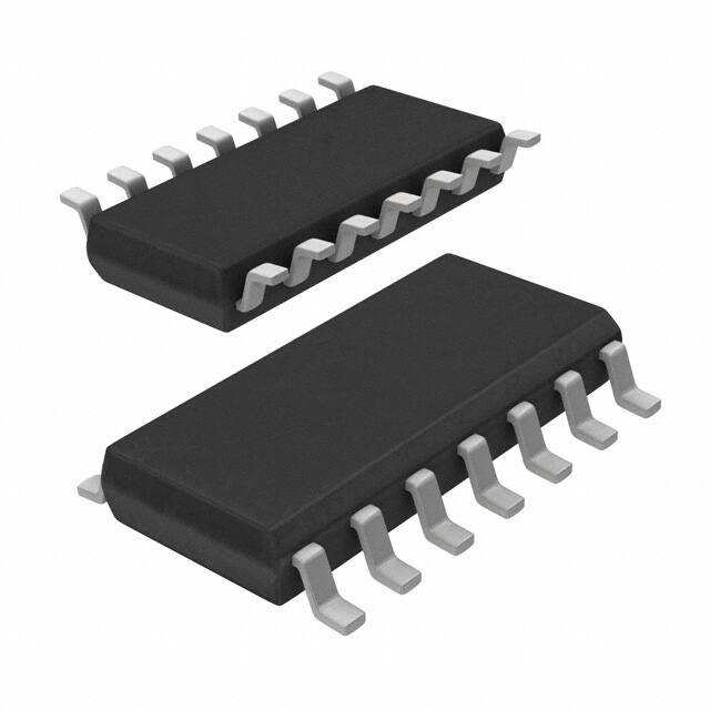


 工商网监
湘ICP备2023018690号
工商网监
湘ICP备2023018690号

