SPD9105W
SPD9105W
http//:www.sh-willsemi.com
1 Lines, Bi-directional, low Capacitance
Transient Voltage Suppressors
Descriptions
The SPD9105W is a low capacitance TVS (Transient Voltage
Suppressor) array designed to protect high speed data
interfaces. It has been specifically designed to protect
sensitive electronic components which are connected to data
and
transmission
lines
from
over-stress
caused
SOD-323
by
Electrostatic Discharge (ESD), cable discharge events (CDE),
lightning and other induced voltage surges.
The SPD9105W incorporates low capacitance steering
diodes that reduce the typical capacitance to 1pF per line.
Pin1
Pin2
The SPD9105W may be used to provide ESD protection up
to ±30kV (contact discharge) according to IEC61000-4-2,
and withstand peak pulse current up to 20A (8/20μs)
according to IEC61000-4-5.
Circuit diagram
The SPD9105W is available in SOD-323 package. Standard
products are Pb-free and Halogen-free.
Features
Stand-off voltage: 5V Max.
Transient protection for each line according to
IEC61000-4-2 (ESD): ±30kV (contact discharge)
* = Month code ( A~Z)
IEC61000-4-5 (surge): 20A (8/20μs).
Low capacitance: CJ = 1pF typ.
Ultra-low leakage current: IR = 0.1nA typ.
Low clamping voltage.
Solid-state silicon technology
Marking (Top View)
Order information
Applications
10/100 Ethernet
STB
Router
Networking
Modem
Will Semiconductor Ltd.
Pin2
W = Device code
IEC61000-4-4 (EFT): 40A - 5/50ns
5 *
Pin1
1
Device
Package
Shipping
SPD9105W-2/TR
SOD-323
3000/Tape&Reel
Revision 1.1, 2014/11/24
�SPD9105W
Absolute maximum ratings
Parameter
Symbol
Rating
Unit
Peak pulse power (tp = 8/20μs)
Ppk
360
W
Peak pulse current (tp = 8/20μs)
IPP
20
A
ESD according to IEC61000-4-2 air discharge
±30
VESD
ESD according to IEC61000-4-2 contact discharge
Junction temperature
TJ
Operating temperature
TOP
Lead temperature
TL
Storage temperature
kV
±30
TSTG
125
o
-40~85
o
260
o
-55~150
o
C
C
C
C
Electrical characteristics (TA = 25 oC, unless otherwise noted)
Parameter
Symbol
Reverse maximum working voltage
VRWM
Reverse leakage current
Reverse breakdown voltage
Clamping voltage
1)
Junction capacitance
1)
IR
VBR
VCL
CJ
Condition
Min.
VRWM = 5V
Typ.
0.1
IT = 1mA
Max.
Unit
5
V
100
nA
5.6
V
IPP = 1A,
tp = 8/20μs
9
V
IPP = 5A,
tp = 8/20μs
11
V
IPP = 20A, tp = 8/20μs
18
V
VR = 0V, f = 1MHz
I/O to I/O
1.0
1.5
pF
According to IEC61000-4-5.
Will Semiconductor Ltd.
2
Revision 1.1, 2014/11/24
�SPD9105W
o
Typical characteristics (TA = 25 C, unless otherwise noted)
Current (%)
Peak pulse current (%)
100
90
Front time: T1= 1.25 × T = 8µs
Time to half-value: T2= 20µs
100
90
50
T2
10
10
0
0
T
T1
tr = 0.7~1ns
Time (µs)
8/20μs waveform per IEC61000-4-5
t
60ns
30ns
20
Time (ns)
Contact discharge current waveform per IEC61000-4-2
1.6
Pulse waveform: tp = 8/20µs
CJ - Junction capacitance (pF)
VC - Clamping voltage (V)
16
14
12
10
8
6
4
0
5
10
15
20
IPP - Peak pulse current (A)
1.4
1.2
1.0
0.8
0.6
0.4
25
f = 1MHz
VAC = 50mV
-3
Clamping voltage vs. Peak pulse current
-2
-1
0
1
2
VR - Reverse voltage (V)
3
Capacitance vs. Reverse voltage
10
1
% of Rated power
Peak pulse power (KW)
100
0.1
80
60
40
20
0.01
0
1
10
100
Pulse time (µs)
1000
25
50
75
100
125
150
o
TA - Ambient temperature ( C)
Non-repetitive peak pulse power vs. Pulse time
Will Semiconductor Ltd.
0
Power derating vs. Ambient temperature
3
Revision 1.1, 2014/11/24
�SPD9105W
o
Typical characteristics (TA=25 C, unless otherwise noted)
ESD clamping
ESD clamping
(+8kV contact discharge per IEC61000-4-2)
(-8kV contact discharge per IEC61000-4-2)
20
TLP current (A)
15
10
5
0
-5
Z0 = 50Ω
tr = 2ns
tp = 100ns
-10
-15
-20
-20
-15
-10
-5
0
5
TLP voltage (V)
10
15
20
TLP Measurement
Will Semiconductor Ltd.
4
Revision 1.1, 2014/11/24
�SPD9105W
Package outline dimensions
SOD-323
Symbol
Dimensions in millimeters
Dimensions in Inches
Min.
Max.
Min.
Max.
A
0.800
1.000
0.031
0.039
A1
0.000
0.100
0.000
0.004
A2
0.800
0.900
0.031
0.035
b
0.250
0.350
0.010
0.014
c
0.080
0.150
0.003
0.006
D
1.200
1.400
0.047
0.055
E
1.600
1.800
0.063
0.071
E1
2.500
2.700
0.098
0.106
0.475 REF
L
0.019 REF
L1
0.250
0.400
0.010
0.016
θ
0°
8°
0°
8°
Recommend land pattern (Unit: mm)
Note: This land pattern is for your reference
only. Actual pad layouts may vary depending
on application.
Will Semiconductor Ltd.
5
Revision 1.1, 2014/11/24
�
很抱歉,暂时无法提供与“SPD9105W-2/TR”相匹配的价格&库存,您可以联系我们找货
免费人工找货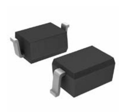


 工商网监
湘ICP备2023018690号
工商网监
湘ICP备2023018690号
