RoHS 2002/95/EC
Vacuum Fluorescent Display Module
Hardware Specification
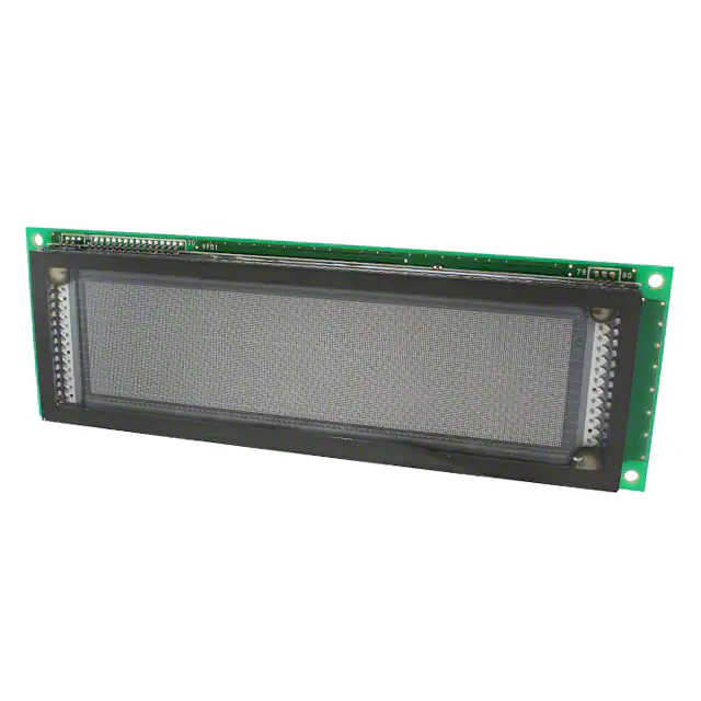
Model: GU256X64E-3900B
Specification No:
DS-1640-0001-01
Date of Issue:
December 02, 2010 (00)
Revision:
March 2, 2011 (01)
Published by
NORITAKE ITRON Corp. / Japan
http://www.noritake-itron.jp
This specification is subject to change without prior notice.
This product complies with RoHS Directive 2002/95/EC
�GU256X64E-3900B Hardware Specification
Contents
1
General Description ..................................................................................................................................... 2
1.1
Scope ........................................................................................................................................................ 2
1.2
Construction ............................................................................................................................................. 2
1.3
Outline....................................................................................................................................................... 2
1.4
Block Diagram ......................................................................................................................................... 2
2
General-purpose I/O port ............................................................................................................................ 3
3
Electrical Specifications ............................................................................................................................. 3
3.1
Absolute Maximum Ratings ................................................................................................................... 3
3.2
Electrical Ratings .................................................................................................................................... 3
3.3
Electrical Characteristics........................................................................................................................ 4
4
Environmental Specifications.................................................................................................................... 5
5
Optical Specifications.................................................................................................................................. 5
6
Physical Specifications ............................................................................................................................... 5
7
Applicable Specifications ........................................................................................................................... 5
8
Interface........................................................................................................................................................... 5
8.1
Interface timing ........................................................................................................................................ 5
8.1.1 Parallel interface timing 1 (Not applicable for bit image data transfer in DMA mode) ..................... 5
8.1.2 Parallel interface timing 2 (Applicable for bit image data transfer in DMA mode) ............................ 6
8.1.3 RS-232 Asynchronous serial interface timing..................................................................................... 6
9
Setup ................................................................................................................................................................ 7
9.1
10
DIP-Switch (SW1) ................................................................................................................................... 7
Connectors ................................................................................................................................................. 7
10.1
Parallel interface & Power connector (CN5) ....................................................................................... 7
10.2
RS-232 Interface & Power connector (CN1) ....................................................................................... 7
10.3
General-purpose I/O port through-holes (CN4) .................................................................................. 7
10.4
Connector position .................................................................................................................................. 8
11 Physical Dimensions ................................................................................................................................... 9
Notice for the Cautious Handling of VFD Modules .................................................................................... 10
Revision history ...................................................................................................................................................11
-1-
�GU256X64E-3900B Hardware Specification
1
General Description
1.1
Scope
This specification covers the hardware aspects of the GU256X64E-3900B vacuum fluorescent graphic
display module.
1.2
Construction
The module consists of a 256 × 64 dot graphic BD-VFD, refresh RAM, character generator, DC/DC
converter, display controller, and all necessary control logic. The module can simultaneously display
graphic patterns and characters on the screen.
1.3
Outline
Power supply:
Interface:
+ 5 VDC only
Parallel interface (CMOS)
Serial interface (Asynchronous, RS-232 -level)
I/O port:
12 bits General-purpose I/O port
Protocol:
Direct mode
Packet mode
Function:
Character display
Graphic display
Control command
Display action command
Draw command
Window function
General-purpose I/O port control
Macro, Program Macro function
Character and Bit Image download function
Memory SW
Display power auto-OFF function
General-purpose data storage
For full details, refer to:
DS-1600-0008-XX: GU-3900B series “General Function” Software Specification.
DS-1600-0006-XX: “Program Macro” software specification.
1.4
Block Diagram
Parallel I/F
Connecter
Parallel
interface IC
RS-232 I/F
Connecter
RS-232
interface IC
Controller
BD-VFD
FROM (32Mbit)
Firmware
Fonts
Memory SW
I/O Port
Through-holes
DIP-SW
VCC
DC/DC
Converter
Anode/Grid
F1 Filament
Note: FROM re-write rating is
GND
approximately 10,000 times.
F2 Filament
-2-
�GU256X64E-3900B Hardware Specification
2
General-purpose I/O port
+5V
General-purpose I/O Port
+5V
VCC
47kΩ
GND
47Ω
Port0-b7
Input/Output port
×8
47kΩ
47Ω
Port0-b0
47kΩ
CPU
47Ω
Port1-b3
Input/Output port
×4
47kΩ
47Ω
Port1-b0
VCC
GND
GU256X64E-3900B
Refer to 3.3 Electrical Characteristics, “General-purpose I/O port supply Voltage”.
For controlling, refer to “General Function” Software Specification, “I/O Port Input / Output setting”, “I/O Port
Output”, and “I/O Port Input”.
3
Electrical Specifications
3.1
Absolute Maximum Ratings
Power Supply Voltage
Parameter
Symbol
Min.
Typ.
Max.
Unit
Power Supply Voltage
VCC
−0.3
-
+6.0
VDC
Symbol
Min.
Typ.
Max.
Unit
Note
Logic Supply Voltage
Parameter
Parallel I/F
D0 – D7, /WR
VpIN
−0.3
-
VCC+0.3
VDC
RS-232 I/F
RXD, DSR
VsIN
−25
-
+25
VDC
Symbol
Min.
Typ.
Max.
Unit
ViIN
−0.3
-
VCC+0.3
VDC
Parameter
Symbol
Min.
Typ.
Max.
Unit
Power Supply Voltage
VCC
4.75
5.0
5.25
VDC
Note
I/O port supply Voltage
Parameter
I/O port
3.2
Port 0, Port 1
Note
Electrical Ratings
All driving voltage for the VFD is converted from the on-board DC/DC converter.
-3-
Note
�GU256X64E-3900B Hardware Specification
3.3
Electrical Characteristics
Logic input/output condition
Measuring Conditions: Ambient temperature = 25 ºC, VCC=5.0VDC
Parameter
Symbol
Min.
IpIH
Logic input current
D0 – D7, /WR
IpIL
VpIH 0.8VCC
Logic input voltage
Parallel I/F
D0 – D7, /WR
VpIL
0
VpOH
3.5
Logic output voltage
RDY
VpOL
0
VsIH
3
Logic input voltage
RXD, DSR
VsIL
−15
VsOH
5
Logic output voltage
RS-232 I/F
TXD, DTR
VsOL
Logic input Impedance
RsIN
3
RXD, DSR
Typ.
-
-
Max.
1.0
−200
VCC
0.2VCC
VCC
0.6
15
−3
−5
-
7
Unit
Condition
uADC
uADC
VDC
VDC
VDC IOH=−10μA
VDC
IOL=4mA
VDC
VDC
VDC
RL=3kΩ
VDC
Note
(1)
-
kΩ
-
(1) “RDY” terminal is open collector (pulled-up by 47kΩ)
VCC1
Module
R47kΩ
Display
Controller
RDY
TR
General-purpose I/O port supply Voltage
Measuring Conditions: Ambient temperature = 25 ºC, VCC=5.0VDC
Parameter
Logic input current
Port 0, 1
General-purpose Logic input voltage
I/O port
Port 0, 1
Logic output voltage
Port 0, 1
Symbol
Min.
Typ.
IiIH
IiIL
ViIH
4.1
ViIL
0
ViOH VCC−0.6
ViOL
-
Max.
1.0
−200
VCC
0.8
0.5
Unit
Condition
μADC
μADC
VDC
VDC
VDC IOH=−200μA
VDC IOL=1.6mA
Note
-
General-purpose I/O port output permissible current
Measuring Conditions: Ambient temperature = 25 ºC, VCC=5.0VDC
Parameter
Symbol
Min.
Typ.
Max.
Unit
Condition
Output permissible
IiOH
1.5
mADC
current Port 0, 1
IiOL
3
mADC
(Single port)
General-purpose
I/O port
Output permissible
IiOH
8
mADC
current Port 0, 1
IiOL
30
mADC
(Sum of all ports)
Output current should not exceed the values in the above table.
If driving LED or other device directly, insert appropriate current limiter into output line.
Note
-
Power Supply condition
Measuring Conditions: Ambient temperature = 25 ºC, VCC=5.0VDC
Parameter
Symbol
Min.
Typ.
Max.
Unit
Condition
Power Supply Current 1
ICC1
1.16
1.50
ADC
All dots ON
Power Supply Current 2
ICC2
0.84
1.09
ADC
All dots OFF
Power Supply Current 3
ICC3
80
120 mADC Display power OFF
Power Consumption
5.8
7.5
W
All dots ON
Note:
The rise time of supply voltage should not exceed 100ms.
Inrush current at power-on may exceed twice normal current.
Display power OFF: Refer to “General Function” Software Specification, “Display power
ON/OFF/auto-OFF” command.
-4-
�GU256X64E-3900B Hardware Specification
4
Environmental Specifications
Operating temperature:
Storage temperature:
Storage humidity:
Vibration (non-operating):
Shock (non-operating):
5
Optical Specifications
Luminance:
Color of illumination:
6
350cd/m2 Min. (700cd/m2 Typ.)
Green (Blue Green)
Physical Specifications
Number of dots:
Display area:
Dot size:
Dot pitch:
Weight:
7
−40 to +70 ºC
−40 to +85 ºC
20 to 80 % R.H (Non Condensing)
10-55-10Hz, all amplitude 1mm, 30 minutes, X-Y-Z
392m/s2 (40G) 9ms X-Y-Z, 3 times each direction
16,384 (256 × 64)
140.65mm × 35.05mm (X × Y)
0.4mm × 0.4mm (X × Y)
0.55mm × 0.55mm (X × Y)
Approximately 210g
Applicable Specifications
Applicable reliability specification: TT-99-3102
Applicable production specification: TT-98-3413
8
Interface
Parallel and RS-232 Serial interfaces are available on this module.
8.1
Interface timing
8.1.1
Parallel interface timing 1 (Not applicable for bit image data transfer in DMA mode)
Min.
100ns
1
/WR
0
Min.
10ns
Min.
50ns
1
D0-D7
0
Max.
500ns
1μs
READY
RDY
BUSY
Note: RDY=0 (BUSY) is output after every byte.
Internal receive buffer capacity is 256 bytes. After data is input, RDY signal is immediately set to
RDY=0 (BUSY) until the received byte is stored to the receive buffer. If the internal receive buffer is
full, RDY signal will remain BUSY until space for 1 byte becomes available. The required time for
this varies, depending on the type of commands and rate at which data is input. The RDY signal
should always be checked before writing data.
-5-
�GU256X64E-3900B Hardware Specification
8.1.2
Parallel interface timing 2 (Applicable for bit image data transfer in DMA mode)
Min.
100ns
Min.
15μs
1
/WR
0
Min.
10ns
Min.
50ns
1
D0-D7
0
Note: Monitoring RDY signal is not necessary for bit image data transfer in DMA mode.
8.1.3
RS-232 Asynchronous serial interface timing
RXD
0
1
Max.
24 bytes
Min.
0μs
Max.
2 bytes
Min.
0μs
READY
DTR
BUSY
TXD
0
1
READY
DSR
BUSY
The above timing is RS-232 level. Logical value is the inverse of the above. (VsIH: 0, VsIL: 1)
Interface:
Baud rate
4800, 9600, 19200, 38400 (default), 57600, 115200bps
(Selected by DIP SW and Memory-SW)
Parity
None (default), Even, Odd
Format
Start (1 bit) + Data (8 bits) [+ Parity (1 bit)] + Stop (1 bit)
Handshake
DTR, DSR
Buffer Capacity
Receive buffer
256 bytes
Transmit buffer
128 bytes
DTR signal change timing
DTR change
1 (READY) → 0 (BUSY)
0 (BUSY) → 1 (READY)
Receive buffer space
32 bytes or less
64 bytes or more
-6-
�GU256X64E-3900B Hardware Specification
9
Setup
9.1
DIP-Switch (SW1)
SW No.
Function
Default
1
Off
2
Off
Display address select
(For multi-connection)
3
Off
4
Off
5
RS-232 interface setting
Off
6
Command mode select
Off
7
Operating Mode select
Off
8
Protocol select
Off
For DIP-SW setup details, refer to “General Function” Software Specification, “Setup”.
10
Connectors
10.1
Parallel interface & Power connector (CN5)
Pin
No.
1
3
5
7
9
11
13
15
10.2
Signal
name
D7
D5
D3
D1
GND
GND
GND
VCC
Function
Direction
Data input
Data input
Data input
Data input
Ground
Ground
Ground
Power supply (5V)
Input
Input
Input
Input
Input
Input
Input
Input
Pin
No.
2
4
6
8
10
12
14
16
Signal
name
D6
D4
D2
D0
/WR
RDY
GND
VCC
Function
Direction
Data input
Data input
Data input
Data input
Data write
Display READY
Ground
Power supply (5V)
Input
Input
Input
Input
Input
Output
Input
Input
Function
Direction
RS-232 Interface & Power connector (CN1)
Pin No.
Signal name
Function
Direction
1
2
3
4
5
6
7
RXD
DTR
DSR
TXD
TEST *
VCC
GND
Data receive
Display busy
Host busy
Data send
TEST (Factory use)
Power supply (5V)
Ground
Input
Output
Input
Output
Input
Input
Input
* Factory use - leave this pin open
10.3
General-purpose I/O port through-holes (CN4)
Pin
No.
1
2
3
4
5
6
7
Signal
name
bit 7
bit 6
bit 5
bit 4
bit 3
bit 2
bit 1
Function
Port 0
Direction
Input /
Output
-7-
Pin
No.
8
9
10
11
12
13
14
Signal
name
bit 0
bit 3
bit 2
bit 1
bit 0
VCC
GND
Port 0
Port 1
Input /
Output
Power supply (5V)
Ground
Input
Input
�GU256X64E-3900B Hardware Specification
10.4
Connector position
pin 1
pin 7
pin 1
pin 2
PCB
RS-232 I/F & Power connector
JST: S7B-XH-A or equivalent
pin 15
PCB
pin 16
Parallel I/F & Power connector
IRISO: IMSA-9032B-16P or equivalent
-8-
�GU256X64E-3900B Hardware Specification
11
Physical Dimensions
-9-
�GU256X64E-3900B Hardware Specification
Notice for the Cautious Handling of VFD Modules
Handling and Usage Precautions:
Please carefully follow the appropriate product application notes and operation standards for proper usage, safe handling, and
maximum performance.
[VFD tubes are made of glass]
The edges of the VFD glass envelope are not smooth, so it is necessary to handle carefully to avoid injuries to hands.
Use caution to avoid breaking the VFD glass envelope, to prevent injury from sharp glass particles.
The tip of the exhaust pipe is fragile so avoid shock from impact.
It is recommended to allow sufficient open space surrounding the exhaust pipe to avoid possible damage.
Please design the PCB for the VFD module within 0.3 mm warping tolerance to avoid any forces that may damage the
display due to PCB distortion causing a breakdown of the electrical circuit leading to VFD failure.
[High voltage]
Avoid touching conductive electrical parts, because the VFD module uses high voltage exceeding 30 – 100 volts.
Even when electric power is turned off, it may take more than one minute for the electrical current to discharge.
[Cable connection]
Do not unplug the power and/or data cables of VFD modules during operation, because unrecoverable damage may
result.
Sending input signals to the VFD module when not powered can cause I/O port damage.
It is recommended to use a 30cm or shorter signal cable to prevent functional failures.
[Electrostatic charge]
VFD modules need electrostatic-free packaging and protection from electrostatic charges during handling and usage.
[Structure]
During operation, VFD and VFD modules generate heat. Please consider sufficient heat radiation dissipation using heat
sink solutions.
Preferably, use UL-grade materials or components in conjunction with VFD modules.
Warp and twist movement causes stress and may break VFDs and VFD modules. Please adhere to allowances within
0.3mm at the point of attachment.
[Power]
Apply regulated power to the VFD module within specified voltages to protect from failures.
VFD modules may draw in-rush current exceeding twice the typical current at power-on, so a power supply with sufficient
capacity and quick starting of the power regulator is recommended.
VFD module needs a specified voltage at the point of connection. Please use an adequate power cable to avoid a
decrease in voltage. As a safety measure, a fuse or other over-current protection is recommended.
[Operating consideration]
Illuminating phosphor will decrease in brightness during extended operation. If a fixed pattern illuminates for an extended
period (several hours), the phosphor efficiency will decrease compared to the non-operating phosphor, causing
non-uniform brightness. Please consider programming the display patterns to use all phosphor segments evenly.
Scrolling may be a consideration for a period of time to refresh the phosphor condition and improve even illumination of
the pixels.
A signal cable 30cm or less is recommended to avoid possible disturbances to the signal.
[Storage and operating environment]
Please use VFD modules under the recommended specified environmental conditions. Salty, sulfuric and dusty
environments may damage the VFD module even during storage.
[Disposal]
VFD uses lead-containing materials (RoHS directive exempts these lead compounds in the glass for electronic devices).
When discarding VFDs or VFD modules, please adhere to applicable laws and regulations.
[Other cautions]
Although the VFD module is designed to be protected from electrical noise, please plan your circuitry to exclude as much
noise as possible.
Do not reconstruct or repair the VFD module without our authorization. We cannot assure the quality or reliability of
unauthorized reconstructed VFD modules.
Notice:
We do not authorize the use of any patents that may be inherent in these specifications.
Neither whole nor partial copying of these specifications is permitted without our approval. If necessary, please ask for
assistance from our sales consultant.
This product is not designed for military, aerospace, medical or other life-critical applications. If you choose to use this
product for these applications, please ask us for prior consultation or we cannot accept responsibility for problems that
may occur.
MBBZ-009-S18A
- 10 -
�GU256X64E-3900B Hardware Specification
Revision history
Specification number
DS-1640-0001-00
DS-1640-0001-01
Date
Dec. 2, 2010
Mar. 2, 2011
Revision
Initial release
·The complementary information (VsIH: 0, VsIL: 1) has been added to "8.1.3
RS-232 Asynchronous serial interface timing".
·“11 Physical Dimensions” has been changed.
·"Notice for the Cautious Handling VFD Modules" has been revised.
- 11 -
�


 工商网监
湘ICP备2023018690号
工商网监
湘ICP备2023018690号
