ASDM4976S
60V N&P-Channel MOSFET
Product Summary
Features
● High power and current handing capability
● N-Channel
● Lead free product is acquired
VDS
RDS(on).TypVGS=10V
RDS(on).TypVGS=4.5V
● Surface mount package
Application
32
V
mΩ
mΩ
6
A
VDS
RDS(on),TypVGS=-10V
-60
RDS(on),TypVGS=-4.5V
ID
82
-6
V
mΩ
mΩ
60
25
ID
● PWM applications
● P-Channel
● Load switch
● Power management
64
A
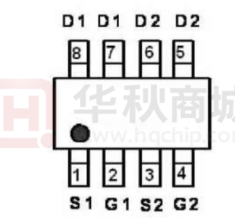
D1 D1 D2 D2
S1 G1 S2 G2
SOP-8
N-channel
top view
P-channel
Absolute Maximum Ratings (TA=25℃unless otherwise noted)
Parameter
Symbol
N-Channel
P-Channel
Unit
Drain-Source Voltage
VDS
60
-60
V
Gate-Source Voltage
VGS
±20
±20
V
Continuous Drain Current
ID
6
-6
A
Pulsed Drain Current (Note 1)
IDM
24
-24
A
2
1.2
W
Maximum Power Dissipation
PD
Operating Junction and Storage Temperature Range
TJ,TSTG
-55 To 150
-55 To 150
℃
Thermal Characteristic
Thermal Resistance,Junction-to-Ambient (Note2)
NOV 2021 Version1.0
1/12
RθJA
N-Ch
89
P-Ch
90
www.ascendsemi.com
℃/W
0755-86970486
�ASDM4976S
60V N&P-Channel MOSFET
N-CH Electrical Characteristics (TA=25℃unless otherwise noted)
Parameter
Symbol
Condition
Min
BVDSS
VGS=0V ID=250μA
60
Zero Gate Voltage Drain Current
IDSS
VDS=48V,VGS=0V
-
Gate-Body Leakage Current
IGSS
VGS=±20V,VDS=0V
-
Gate Threshold Voltage
VGS(th)
VDS=VGS,ID=250μA
Drain-Source On-State Resistance
RDS(ON)
Typ
Max
Unit
-
V
-
1
μA
-
±100
nA
1.6
2.5
V
Off Characteristics
Drain-Source Breakdown Voltage
On Characteristics (Note 3)
Forward Transconductance
gFS
1
VGS=10V, ID=4A
-
25
30
mΩ
VGS=4.5V, ID=2A
-
32
40
mΩ
VDS=10V, ID=4.5A
-
20
-
S
-
1040
-
PF
-
170
-
PF
-
132
-
PF
-
4.5
-
nS
Dynamic Characteristics (Note4)
Input Capacitance
Clss
Output Capacitance
Coss
Reverse Transfer Capacitance
Crss
VDS=25V,VGS=0V,
F=1.0MHz
Switching Characteristics (Note 4)
Turn-on Delay Time
td(on)
Turn-on Rise Time
tr
VDD=15V, RL=3Ω
-
2.5
-
nS
td(off)
VGS=10V,RGEN=3Ω
-
14.5
-
nS
-
3.5
-
nS
-
5.2
-
nC
-
0.85
-
nC
-
1.3
-
nC
-
-
1.3
V
-
-
6
A
Turn-Off Delay Time
Turn-Off Fall Time
tf
Total Gate Charge
Qg
Gate-Source Charge
Qgs
Gate-Drain Charge
Qgd
VDS=30V,ID=4.5
A, VGS=10V
Drain-Source Diode Characteristics
Diode Forward Voltage (Note 3)
VSD
Diode Forward Current (Note 2)
IS
NOV 2021 Version1.0
2/12
VGS=0V,IS=3A
www.ascendsemi.com
0755-86970486
�ASDM4976S
60V N&P-Channel MOSFET
P-CH Electrical Characteristics (TA=25℃unless otherwise noted)
�����������������������
Parameter
Symbol
Condition
Min
Drain-Source Breakdown Voltage
BVDSS
VGS=0V ID=-250μA
-60
Zero Gate Voltage Drain Current
IDSS
VDS=-48V , VGS=0V
-
Gate-Body Leakage Current
IGSS
VGS=±20V,VDS=0V
Gate Threshold Voltage
VGS(th)
Drain-Source On-State Resistance
RDS(ON)
Typ
Max
Unit
-
V
-
-1
μA
-
-
±100
nA
VDS=VGS,ID=-250μA
-1
-1.8
-2.5
V
VGS=-10V, ID=-3.5A
-
64
70
mΩ
VGS=-4.5V, ID=-3.1A
-
82
90
mΩ
VGS=-5V, ID=-3.5A
12
-
-
S
-
988
-
PF
-
168
-
PF
-
102
-
PF
-
9
-
nS
Off Characteristics
On Characteristics (Note 3)
Forward Transconductance
gFS
Dynamic Characteristics (Note4)
InputCapacitance
Clss
OutputCapacitance
Coss
Reverse Transfer Capacitance
Crss
VDS=-15V,VGS=0V,
F=1.0MHz
Switching Characteristics (Note 4)
Turn-on Delay Time
td(on)
Turn-on Rise Time
tr
VDD=-15V,RL=3.6Ω
-
5
-
nS
td(off)
VGS=-10V,RGEN=3Ω
-
28
-
nS
Turn-Off Delay Time
Turn-Off Fall Time
tf
-
13.5
-
nS
Total Gate Charge
Qg
-
14
-
nC
Gate-Source Charge
Qgs
-
3.1
-
nC
Gate-Drain Charge
Qgd
-
3.
-
nC
-
-
-1.3
VDS=-30V,ID=-3.5A,VGS=-10V
Drain-Source Diode Characteristics
Diode Forward Voltage (Note 3)
VSD
V=
GS=0V,IS -1A
V
Notes:
1. Repetitive Rating: Pulse width limited by maximum junction temperature.
2. Surface Mounted on FR4 Board, t ≤ 10 sec.
3. Pulse Test: Pulse Width ≤ 300μs, Duty Cycle ≤ 2%.
4. Guaranteed by design, not subject to production
NOV 2021 Version1.0
3/12
www.ascendsemi.com
0755-86970486
�ASDM4976S
60V N&P-Channel MOSFET
N-Channel Typical Electrical and Thermal Characteristics
ton
Vdd
Vin
Vgs
Rgen
D
tr
td(on)
Rl
Vout
tf
td(off)
90%
VOUT
G
S
90%
INVERTED
10%
10%
90%
VIN
50%
10%
50%
PULSE WIDTH
Figure 2:Switching Waveforms
Figure 1:Switching Test Circuit
ID- Drain Current (A)
ID- Drain Current (A)
toff
Vgs Gate-Source Voltage (V)
Vds Drain-Source Voltage (V)
Figure 4 Transfer Characteristics
Normalized On-Resistance
Rdson On-Resistance(mΩ)
Figure 3 Output Characteristics
ID- Drain Current (A)
Figure 5 Drain-Source On-Resistance
NOV 2021 Version1.0
4/12
TJ-Junction Temperature(℃)
Figure 6 Drain-Source On-Resistance
www.ascendsemi.com
0755-86970486
�ASDM4976S
Rdson On-Resistance(mΩ)
C Capacitance (pF)
60V N&P-Channel MOSFET
TJ-Junction Temperature(℃)
Vgs Gate-Source Voltage (V)
Figure 8 Drain-Source On-Resistance
Vgs Gate-Source Voltage (V)
Is- Reverse Drain Current (A)
Figure7 Rdson vs Vgs
Vds Drain-Source Voltage (V)
Qg Gate Charge (nC)
Figure 10 Source- Drain Diode Forward
ID- Drain Current (A)
C Capacitance (pF)
Figure 9 Gate Charge
Vds Drain-Source Voltage (V)
Figure 11 Capacitance vs Vds
NOV 2021 Version1.0
5/12
Vds Drain-Source Voltage (V)
Figure 12
Safe Operation Area
www.ascendsemi.com
0755-86970486
�ASDM4976S
r(t),Normalized Effective
Transient Thermal Impedance
60V N&P-Channel MOSFET
Square Wave Pluse Duration(sec)
Figure 13 Normalized Maximum Transient Thermal Impedance
NOV 2021 Version1.0
6/12
www.ascendsemi.com
0755-86970486
�ASDM4976S
60V N&P-Channel MOSFET
P-Channel Typical Electrical and Thermal Characteristics
ton
tr
td(on)
toff
tf
td(off)
90%
VOUT
90%
INVERTED
10%
10%
90%
VIN
50%
10%
50%
PULSE WIDTH
Figure 2:Switching Waveforms
PD Power(W)
ID- Drain Current (A)
Figure 1:Switching Test Circuit
TJ-Junction Temperature(℃)
TJ-Junction Temperature(℃)
Figure 4 Drain Current
ID- Drain Current (A)
Rdson On-Resistance(mΩ)
Figure 3 Power Dissipation
Vds Drain-Source Voltage (V)
Figure 5 Output CHARACTERISTICS
NOV 2021 Version1.0
7/12
ID- Drain Current (A)
Figure 6 Drain-Source On-Resistance
www.ascendsemi.com
0755-86970486
�ASDM4976S
ID- Drain Current (A)
Normalized On-Resistance
60V N&P-Channel MOSFET
TJ-Junction Temperature(℃)
Vgs Gate-Source Voltage (V)
Figure 8 Drain-Source On-Resistance
C Capacitance (pF)
Rdson On-Resistance(mΩ)
Figure 7 Transfer Characteristics
Vgs Gate-Source Voltage (V)
Vds Drain-Source Voltage (V)
Figure 10 Capacitance vs Vds
Vgs Gate-Source Voltage (V)
Is- Reverse Drain Current (A)
Figure 9 Rdson vs Vgs
Qg Gate Charge (nC)
Figure 11 Gate Charge
NOV 2021 Version1.0
8/12
Vsd Source-Drain Voltage (V)
Figure 12 Source- Drain Diode Forward
www.ascendsemi.com
0755-86970486
�ASDM4976S
ID- Drain Current (A)
60V N&P-Channel MOSFET
Vds Drain-Source Voltage (V)
Safe Operation Area
r(t),Normalized Effective
Transient Thermal Impedance
Figure 13
Square Wave Pluse Duration(sec)
Figure 14 Normalized Maximum Transient Thermal Impedance
NOV 2021 Version1.0
9/12
www.ascendsemi.com
0755-86970486
�ASDM4976S
60V N&P-Channel MOSFET
Ordering and Marking Information
Ordering Device No.
Marking
Package
ASDM4976S-R
4976
SOP-8
Quantity
Tape&Reel
4000/Reel
MARKING
PACKAGE
SOP-8
NOV 2021 Version1.0
Packing
4976
10/12
www.ascendsemi.com
0755-86970486
�ASDM4976S
60V N&P-Channel MOSFET
SOP-8 PACKAGE IN FORMATION
NOV 2021 Version1.0
11/12
www.ascendsemi.com
0755-86970486
�ASDM4976S
60V N&P-Channel MOSFET
IMPORTANT NOTICE
ShenZhen Ascend Semiconductor incorporated MAKES NO WARRANTY OF ANY KIND, EXPRESS OR IMPLIED, WITH REGARDS TO THIS
DOCUMENT, INCLUDING, BUT NOT LIMITED TO, THE IMPLIED WARRANTIES OF MERCHANTABILITY AND FITNESS FOR A PARTICULAR
PURPOSE (AND THEIR EQUIVALENTS UNDER THE LAWS OF ANY JURISDICTION).
ShenZhen Ascend Semiconductor Incorporated and its subsidiaries reserve the right to make modifications, enhancements, improvements,
corrections or other changes without further notice to this document and any product described herein. ShenZhen Ascend Semiconductor
Incorporated does not assume any liability arising out of the application or use of this document or any product described herein; neither
does ShenZhen Ascend Semiconductor Incorporated convey any license under its patent or trademark rights, nor the rights of others. Any
Customer or user of this document or products described herein in such applications shall assume .
all risks of such use and will agree to hold Ascendsemi Incorporated and all the companies whose products are represented on ShenZhen
Ascend Semiconductor Incorporated website, harmless against all damages.
ShenZhen Ascend Semiconductor Incorporated does not warrant or accept any liability whatsoever in respect of any products purchased
through unauthorized sales channel. Should Customers purchase or use ShenZhen Ascend Semiconductor Incorporated products for any
unintended or unauthorized application, Customers shall indemnify and hold ShenZhen Ascend Semiconductor Incorporated and its
representatives harmless against all claims, damages, expenses, and attorney fees arising out of, directly or indirectly, any claim of personal
injury or death associated with such unintended or unauthorized application.
www.ascendsemi.com
NOV 2021 Version1.0
12/12
www.ascendsemi.com
0755-86970486
�


 工商网监
湘ICP备2023018690号
工商网监
湘ICP备2023018690号
