ASDM60DN05S
60V Dual N-CHANNEL MOSFET
Features
Product Summary
• Dual N-Channel,5V Logic Level Control
• Enhancement mode
V
• Fast Switching
• High Effective
60
V
RDS(on),Typ@ VGS =10 V
28
mΩ
ID
5
A
DS
Application
• Power Management in Inverter System
• Synchronous Rectification
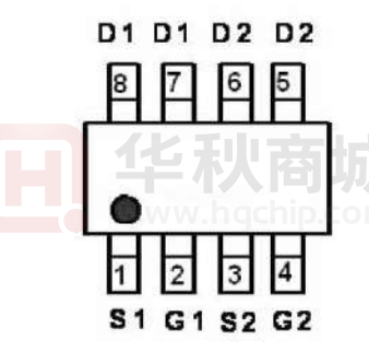
Dual N-Channel MOSFET
SOP8
Absolute Maximum Ratings
Parameter
Symbol
Rating
Unit
Common Ratings (TA=25°C Unless Otherwise Noted)
VDSS
Drain-Source Voltage
60
VGSS
Gate-Source Voltage
±20
Maximum Junction Temperature
150
°C
-55 to 150
°C
TJ
TSTG
Storage Temperature Range
IS
Diode Continuous Forward Current
V
TA=25°C
5.0
A
TA=25°C
20
A
TA=25°C
5.0
TA=70°C
7.0
TA=25°C
3
TA=70°C
1.6
Mounted on Large Heat Sink
①
300μs Pulse Drain Current Tested
②
ID
Continuous Drain Current(VGS=10V)
PD
Maximum Power Dissipation
IDP
RJC
RJA
③
A
W
Thermal Resistance-Junction to Case
36
°C/W
Thermal Resistance-Junction to Ambient
85
°C/W
-
mJ
Drain-Source Avalanche Ratings
④
EAS
Avalanche Energy, Single Pulsed
NOV 2018 Version1.0
1/7
Ascend Semicondutor Co.,Ltd
�ASDM60DN05S
60V Dual N-CHANNEL MOSFET
Electrical Characteristics (TA=25°C Unless Otherwise Noted)
Symbol
Parameter
Test Condition
Min.
Typ.
Max.
Unit
Static Characteristics
BVDSS
IDSS
Drain-Source Breakdown Voltage VGS=0V, IDS=250µA
Zero Gate Voltage Drain Current
VDS=VGS, IDS=250µA
IGSS
Gate Leakage Current
VGS=±20V, VDS=0V
Drain-Source On-state Resistance
1
TJ=125°C
Gate Threshold Voltage
⑤
V
VDS=60V, VGS=0V
VGS(th)
RDS(ON)
60
µA
30
1
1.6
2.5
V
±100
nA
VGS=10V, IDS=8.0A
28
30
mΩ
VGS=4.5V, IDS=6A
31
36
mΩ
1
V
Diode Characteristics
⑤
VSD
Diode Forward Voltage
trr
Reverse Recovery Time
Qrr
Reverse Recovery Charge
ISD=10A, VGS=0V
ISD=10A, dlSD/dt=100A/µs
25
ns
14
nC
1
Ω
⑥
Dynamic Characteristics
RG
Gate Resistance
VGS=0V,VDS=0V,F=1MHz
Ciss
Input Capacitance
Coss
Output Capacitance
Crss
Reverse Transfer Capacitance
VGS=0V,
VDS=30V,
Frequency=1.0MHz
td(ON)
Turn-on Delay Time
tr
Turn-on Rise Time
td(OFF)
Turn-off Delay Time
tf
pF
53
VDD=30V,IDS=8.0A,
VGEN=10V,RG=3Ω
45
24
ns
17
⑥
Qg
Total Gate Charge
Qgs
Gate-Source Charge
Qgd
Gate-Drain Charge
Notes:
120
10
Turn-off Fall Time
Gate Charge Characteristics
1040
VDS=48V, VGS=10V,
IDS=8.0A
25
4.5
nC
6.5
①Pulse width limited by safe operating area.
②Calculated continuous current based on maximum allowable junction temperature.
③When mounted on 1 inch square copper board, t≤10sec. The value in any given application
depends on the user's specific board design.
④Limited by TJmax. Starting TJ = 25°C.
⑤Pulse test;Pulse width≤300µs, duty cycle≤2%.
⑥Guaranteed by design, not subject to production testing.
NOV 2018 Version1.0
2/7
Ascend Semicondutor Co.,Ltd
�ASDM60DN05S
60V Dual N-CHANNEL MOSFET
Typical Characteristics
Power Dissipation
Drain Current
12
10
ID - Drain Current (A)
PD - Power (W)
3
2
1
8
6
4
2
VGS=10V
0
0
0
25
50
75
100
125
25
150
50
10µs
100µs
1ms
10ms
DC
1
0.1
TA=25°C
0.1
1
10
RDS(ON) - On - Resistance (mΩ)
Safe Operation Area
RDS(ON) limited
ID - Drain Current (A)
10
100
125
150
TJ - Junction Temperature (°C)
TJ - Junction Temperature (°C)
100
75
Drain Current
60
IDS=10A
50
40
30
20
10
0
0
100
1
2
3
4
5
6
7
8
9
10
VGS - Gate-Source Voltage (V)
VDS - Drain-Source Voltage (V)
ZthJA - Thermal Response (°C/W)
Thermal Transient Impedance
1000
Duty=0.5, 0.2, 0.1, 0.05, 0.02, 0.01, Single Pulse
100
10
1
Single Pulse
RθJA=50°C/W
0.1
0.0001
0.001
0.01
0.1
1
10
100
Square Wave Pulse Duration (sec)
NOV 2018 Version1.0
3/7
Ascend Semicondutor Co.,Ltd
�ASDM60DN05S
60V Dual N-CHANNEL MOSFET
Typical Characteristics
Output Characteristics
6V
ID - Drain Current (A)
10V
4.5V
40
4V
30
3.5V
20
10
3V
0
0
1
3
Drain-Source On Resistance
60
RDS(ON) - On Resistance (mΩ)
50
4
50
40
VGS=4.5V
30
VGS=10V
20
10
0
0
10
20
VDS - Drain-Source Voltage (V)
2.0
Drain-Source On Resistance
1.5
1.0
TJ=25°C
Rds(on)=20mΩ
TJ=150°C
1
TJ=25°C
0.1
0.01
0.0
-50
-25
0
25
50
75
100
125
0.2
150
0.4
Capacitance
VGS - Gate-Source Voltage (V)
C - Capacitance (pF)
Frequency=1.0MHz
Ciss
900
600
300
Coss
Crss
0
10
1
100
1
1.2
1.4
10
VDS=24V
IDS=20A
9
8
7
6
5
4
3
2
1
0
0
VDS - Drain-Source Voltage (V)
NOV 2018 Version1.0
0.8
Gate Charge
1800
1200
0.6
VSD - Source-Drain Voltage (V)
TJ - Junction Temperature (°C)
1500
50
Source-Drain Diode Forward
10
VGS=10V
IDS=8.0A
0.5
40
ID - Drain Current (A)
IS - Source Current (A)
Normalized On Resistance
2.5
30
10
20
30
40
QG - Gate Charge (nC)
4/7
Ascend Semicondutor Co.,Ltd
�ASDM60DN05S
60V Dual N-CHANNEL MOSFET
Ordering and Marking Information
Ordering Device No.
Marking
Package
ASDM60DN05S-R
60DN05
SOP-8
Quantity
Tape&Reel
4000/Reel
MARKING
PACKAGE
SOP-8
NOV 2018 Version1.0
Packing
60DN05
5/7
Ascend Semicondutor Co.,Ltd
�ASDM60DN05S
60V Dual N-CHANNEL MOSFET
SOP-8 PACKAGE IN FORMATION
NOV 2018 Version1.0
6/7
Ascend Semicondutor Co.,Ltd
�ASDM60DN05S
60V Dual N-CHANNEL MOSFET
IMPORTANT NOTICE
Xi‘an Ascend Semiconductor incorporated MAKES NO WARRANTY OF ANY KIND, EXPRESS OR IMPLIED, WITH REGARDS TO THIS
DOCUMENT, INCLUDING, BUT NOT LIMITED TO, THE IMPLIED WARRANTIES OF MERCHANTABILITY AND FITNESS FOR A PARTICULAR
PURPOSE (AND THEIR EQUIVALENTS UNDER THE LAWS OF ANY JURISDICTION).
Xi‘an Ascend Semiconductor Incorporated and its subsidiaries reserve the right to make modifications, enhancements, improvements, corrections
or other changes without further notice to this document and any product described herein. Xi‘an Ascend Semiconductor Incorporated does not
assume any liability arising out of the application or use of this document or any product described herein; neither does Xi‘an Ascend
Semiconductor Incorporated convey any license under its patent or trademark rights, nor the rights of others. Any Customer or user of this
document or products described herein in such applications shall assume .
all risks of such use and will agree to hold Ascendsemi Incorporated and all the companies whose products are represented on Xi‘an
Ascend Semiconductor Incorporated website, harmless against all damages.
Xi‘an Ascend Semiconductor Incorporated does not warrant or accept any liability whatsoever in respect of any products purchased through
unauthorized sales channel. Should Customers purchase or use Xi‘an Ascend Semiconductor Incorporated products for any unintended or
unauthorized application, Customers shall indemnify and hold Xi‘an Ascend Semiconductor Incorporated and its representatives harmless against
all claims, damages, expenses, and attorney fees arising out of, directly or indirectly, any claim of personal injury or death associated with such
unintended or unauthorized application.
www.ascendsemi.com
NOV 2018 Version1.0
7/7
Ascend Semicondutor Co.,Ltd
�


 工商网监
湘ICP备2023018690号
工商网监
湘ICP备2023018690号
