1-Line Bi-directional TVS Diode
PESDHC2FD15VUF
Description
Features
The PESDHC2FD15VUF is a 15V bi-directional TVS
diode,
utilizing
leading
monolithic
silicon
technology to provide fast response time and low
ESD clamping voltage, making this device an
ideal solution for protecting voltage sensitive
data and power line. The PESDHC2FD15VUF complies
with the IEC 61000-4-2 (ESD) standard with
±30kV air and ±30kV contact discharge. It is
assembled into an ultra-small 1.0 x 0.6 x 0.5mm
lead-free DFN package. The small size and high
ESD surge protection make PESDHC2FD15VUF an ideal
choice to protect cell phone, digital cameras,
audio
players
and
many
other
portable
applications.
Ultra small package: 1.0 x0.6 x0.5mm
Protects one data or power line
Ultra low leakage:nA level
Mechanical Characteristics
Applications
Package: DFN1006-2 (1.0 x0.6 x0.5mm)
Case Material: “Green” Molding Compound.
Moisture Sensitivity: Level 3 per J-STD-020
Terminal Connections: See Diagram Below
Marking Information: See Below
Dimensions and Pin Configuration
Operating voltage:15V
Low clamping voltage
2-pin leadless package
Complies with following standards:
– IEC 61000-4-2 (ESD) immunity test
Air discharge: ±30kV
Contact discharge: ±30kV
– IEC61000-4-5 (Lightning) 5A (8/20µs)
RoHS Compliant
Cellular Handsets and Accessories
Personal Digital Assistants
Notebooks and Handhelds
Portable Instrumentation
Digital Cameras
Peripherals
Audio Players
Marking Information
22 *
22 = Device Marking Code
Package Dimensions
Circuit and Pin Schematic
Ordering Information
Part Number
Marking
Packaging
Reel Size
PESDHC2FD15VUF
22
10000/Tape & Reel
7 inch
Rev. 1_Mar, 2019
1
�PESDHC2FD15VUF
1-Line Bi-directional TVS Diode
Absolute Maximum Ratings (TA=25°C unless otherwise specified)
Parameter
Symbol
Value
Unit
Peak Pulse Power(8/20µs)
Ppk
100
W
Peak Pulse Current(8/20µs)
IPP
5
A
ESD per IEC 61000−4−2 (Air)
±30
VESD
ESD per IEC 61000−4−2 (Contact)
Operating Temperature Range
Storage Temperature Range
±30
TJ
−55 to +125
°C
Tstg
−55 to +150
°C
Electrical Characteristics (TA=25°C unless otherwise specified)
Parameter
Reverse Working Voltage
Breakdown Voltage
Symbol
Min
Typ
VRWM
VBR
Max
Unit
15
V
13.3
Test Condition
V
IT = 1mA
Reverse Leakage Current
IR
0.2
μA
VRWM = 12V
Clamping Voltage
VC
16
V
IPP = 1A (8 x 20µs pulse)
Clamping Voltage
VC
20
V
IPP = 5A (8 x 20µs pulse)
Junction Capacitance
CJ
15
pF
VR = 0V, f = 1MHz
Rev. 1_Mar, 2019
7.5
2
kV
�1-Line Bi-directional TVS Diode
PESDHC2FD15VUF
Typical Performance Characteristics (TA=25℃ unless otherwise Specified)
Junction Capacitance vs. Reverse Voltage
Peak Pulse Power vs. Pulse Time
Clamping Voltage vs. Peak Pulse Current
Power Derating Curve
100
% of Peak Pulse Current
90
80
70
60
50
40
30
20
10
0
0
20
40
Time_t(uS)
60
80
ESD Clamping Voltage
8 X 20μs Pulse Waveform
Rev. 1_Mar, 2019
8 kV Contact per IEC61000−4−2
3
�1-Line Bi-directional TVS Diode
PESDHC2FD15VUF
DFN1006-2 Package Outline Drawing
A
DIMENSIONS
MILLIMETERS
INCHES
MIN
NOM
MAX
MIN
NOM
MAX
0.450
0.500
0.550
0.018
0.020
0.022
A1
0.000
0.020
0.050
0.000
0.001
0.002
b
0.450
0.50
0.550
0.018
0.020
0.022
c
0.120
0.150
0.180
0.005
0.006
0.007
D
0.950
1.000
1.050
0.037
0.039
0.041
SYM
e
0.65 BSC
0.026 BSC
E
0.55
0.60
0.65
0.022
0.024
0.026
L
0.20
0.25
0.30
0.008
0.010
0.012
L1
0.05REF
h
0.07
0.12
0.002REF
0.17
0.003
0.005
Suggested Land Pattern
SYM
Rev. 1_Mar, 2019
DIMENSIONS
MILLIMETERS
INCHES
X
0.60
0.024
Y1
0.50
0.020
Y2
0.30
0.012
Y3
0.80
0.032
Z
1.30
0.052
4
0.007
�
很抱歉,暂时无法提供与“PESDHC2FD15VUF”相匹配的价格&库存,您可以联系我们找货
免费人工找货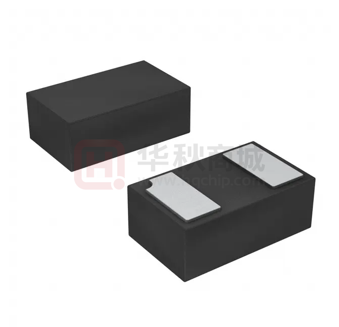


 工商网监
湘ICP备2023018690号
工商网监
湘ICP备2023018690号
