TPA626
Bi-Directional Current and Power Monitor
Features
Description
Senses Bus Voltages From 0V to 36V
The TPA626 is a current and power monitor, with I 2C
High-Side or Low-Side Sensing
or SMBUS-compatible interface. The device monitors
Reports Current, Voltage, and Power
both a shunt voltage drop and bus supply voltage.
High Accuracy
Configurable Averaging Options
16 Programmable Addresses
The TPA626 common mode input voltage can vary
from 0V to 36V.
The TPA626 features up to 16 programmable
addresses on the I2C-compatible interface.
Operates from 2.7-V to 5.5-V Power Supply
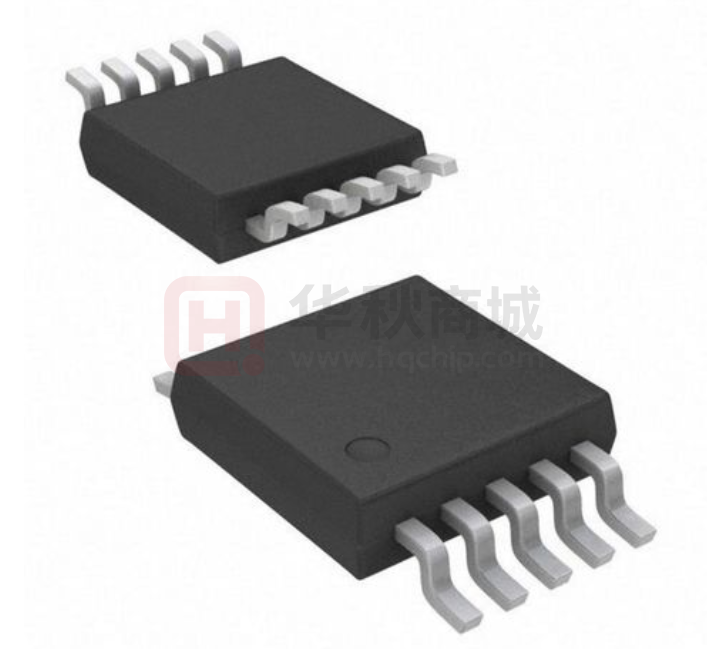
10-Pin, MSOP Package
Applications
Power management
Servers
Telecom Equipment
Computing
Test Equipment
www.3peakic.com.cn
1 / 20
Rev.A.06
�TPA626
Bi-Directional Current and Power Monitor
Function block or application schematic
Figure 1.
www.3peakic.com.cn
2 / 20
Rev.A.06
�TPA626
Bi-Directional Current and Power Monitor
Table of Contents
Features ......................................................................................................................................................................... 1
Applications .................................................................................................................................................................. 1
Description .................................................................................................................................................................... 1
Function block or application schematic ................................................................................................................... 2
Table of Contents .......................................................................................................................................................... 3
Pin Configuration and Functions ................................................................................................................................ 4
Pin Functions ...........................................................................................................................................................................4
Order Information ......................................................................................................................................................... 4
Absolute Maximum Ratings ......................................................................................................................................... 5
ESD, Electrostatic Discharge Protection .................................................................................................................... 5
Recommended Operating Conditions......................................................................................................................... 5
Thermal Information ..................................................................................................................................................... 6
Electrical Characteristics ............................................................................................................................................. 7
Electrical Characteristics ............................................................................................................................................. 8
Typical Performance Characteristics .......................................................................................................................... 9
Detailed description.................................................................................................................................................... 11
Programming ........................................................................................................................................................ 11
I2C address ........................................................................................................................................................... 11
Register map ......................................................................................................................................................... 12
Tape And Reel Information ......................................................................................................................................... 18
Package Outline Dimensions ..................................................................................................................................... 19
Revision History ......................................................................................................................................................... 20
www.3peakic.com.cn
3 / 20
Rev.A.06
�TPA626
Bi-Directional Current and Power Monitor
Pin Configuration and Functions
MSOP10
A1 1
10 IN+
A0 2
9 IN-
Alert 3
8 VBUS
SDA 4
7 GND
SCL 5
6 VS
Pin Functions
PIN
I/O
DESCRIPTION
NAME
NO.
A0
2
Digital input
Address pin. Connect to GND, SCL, SDA, or VS.
A1
1
Digital input
Address pin. Connect to GND, SCL, SDA, or VS.
Alert
3
Digital output
Multi-functional alert, open-drain output.
GND
7
IN+
10
Analog input
Connect to supply side of shunt resistor.
IN–
9
Analog input
Connect to load side of shunt resistor.
SCL
5
Digital input
Serial bus clock line, open-drain input.
SDA
4
Digital I/O
Serial bus data line, open-drain input/output.
VBUS
8
Analog input
VS
6
Analog
Ground.
Bus voltage input.
Analog
Power supply, 2.7 V to 5.5 V.
Order Information
Model Name
Order Number
Package
MSL Level
Transport Media, Quantity
Marking
Information
TPA626
TPA626-VR-S
www.3peakic.com.cn
MSOP10
1
4 / 20
Tape and Reel, 3000
TPA626
Rev.A.06
�TPA626
Bi-Directional Current and Power Monitor
Absolute Maximum Ratings
Cover operating free-air temperature range (unless otherwise noted)
(1)
MIN
VVS
Supply voltage
Differential (V IN+ – V IN-
) (2)
MAX
UNIT
6
V
–40
40
–0.3
40
VVBUS
–0.3
40
V
VSDA
GND – 0.3
6
V
VSCL
GND – 0.3
VVS + 0.3
V
Analog Inputs,
IN+, IN–
Common-Mode (V IN+ + VIN-) / 2
V
IIN
Input current into any pin
5
mA
IOUT
Open-drain digital output current
10
mA
TJ
Junction temperature
150
°C
Tstg
Storage temperature range
150
°C
(1)
(2)
–65
Stresses beyond those listed under Absolute Maximum Ratings may cause permanent damage to the device. These are stress ratings only,
which do not imply functional operation of the device at these or any other conditions beyond those indicated under Recommended Operating
Conditions. Exposure to absolute-maximum-rated conditions for extended periods may affect device reliability.
IN+ and IN– may have a differential voltage between –40 V and 40 V. However, the voltage at these pins must not exceed the range
–0.3 V to 40 V.
ESD, Electrostatic Discharge Protection
VALUE
Human body model (HBM), per ANSI/ESDA/JEDEC JS-001, all pins (1)
±2000
Charged device model (CDM), per JEDEC specification JESD22-C101, all
pins (2)
±1000
UNIT
Electrostatic
V(ESD)
V
Recommended Operating Conditions
Min
Typ
Max
Unit
Common mode input
VCM
12
V
3.3
V
voltage
VVS
Operating supply
voltage
Operating free-air
TA
-40
125
temperature
www.3peakic.com.cn
5 / 20
Rev.A.06
�TPA626
Bi-Directional Current and Power Monitor
Thermal Information
Package Type
θJA
θJC
Unit
MSOP10
171
42.9
°C/W
www.3peakic.com.cn
6 / 20
Rev.A.06
�TPA626
Bi-Directional Current and Power Monitor
Electrical Characteristics
TA = 25°C, VVS = 3.3 V, VIN+ = 12 V, VSENSE = (VIN+ – VIN–) = 0 mV and VVBUS = 12 V, unless otherwise noted
PARAMETER
TEST CONDITIONS
MIN
TYP
MAX
UNIT
mV
INPUT
Shunt voltage input range
–81.9175
81.92
Bus voltage input range (1)
0
36
0 V ≤ VIN+ ≤ 36 V
CMRR
Common-mode rejection
VOS
Shunt offset voltage, RTI (2)
Shunt offset voltage, RTI (2) vs
temperature
PSRR
Shunt offset voltage, RTI(2) vs power
120
140
±2.5
–40°C ≤ TA ≤ 125°C
2.7 V ≤ VS ≤ 5.5 V
V
dB
±30
μV
μV/°C
0.15
μV/V
5
supply
VOS
Bus offset voltage, RTI (2)
±10
Bus offset voltage, RTI (2) vs
temperature
PSRR
Bus offset voltage,
RTI (2)
–40°C ≤ TA ≤ 125°C
vs power
±20
mV
60
μV/°C
1
mV/V
supply
IB
Input bias current
10
VBUS input impedance
Input leakage
(3)
(IN+ pin) + (IN– pin),
Power-down mode
μA
830
kΩ
1
μA
16
Bits
2.5
μV
1.25
mV
DC ACCURACY
ADC native resolution
1 LSB step size
Shunt voltage
Bus voltage
Shunt voltage gain error
Shunt voltage gain error
vs temperature
0.02%
–40°C ≤ TA ≤ 125°C
50
Shunt voltage linearity
0.02%
–40°C ≤ TA ≤ 125°C
ADC conversion time
www.3peakic.com.cn
0.4%
50
Bus voltage linearity
tCT
ppm/°C
0.5%
Bus voltage gain error
Bus voltage gain error vs
temperature
0.4%
ppm/°C
0.5%
CT bit = 000
66
CT bit = 001
134
CT bit = 010
269
7 / 20
μs
Rev.A.06
�TPA626
Bi-Directional Current and Power Monitor
CT bit = 011
542
CT bit = 100
1085
CT bit = 101
2170
CT bit = 110
4341
CT bit = 111
8682
μs
SMBus
SMBus timeout (4)
(1)
(2)
(3)
(4)
(5)
28
ms
While the input range is 36 V, the full-scale range of the ADC scaling is 40.96 V.
RTI = Referred-to-input.
Input leakage is positive (current flowing into the pin) for the conditions shown at the top of this table. Negative leakage currents can
occur under different input conditions.
SMBus timeout in the TPA626 resets the interface any time SCL is low for more than 28 ms.
Test Levels: (A) Tested at final test. Over temperature limits are set by characterization and simulation. (B) Set by
characterization and simulation. (C) Typical value only for information, provided by design simulation.
Electrical Characteristics
TA = 25°C, VVS = 3.3 V, VIN+ = 12 V, VSENSE = (VIN+ – VIN–) = 0 mV and VVBUS = 12 V, unless otherwise noted
PARAMETER
TEST
MIN
TYP
MAX
UNIT
CONDITIONS
DIGITAL INPUT/OUTPUT
Input capacitance
Leakage input current
VIH
High-level input voltage
VIL
Low-level input voltage
VOL
Low-level output voltage, SDA, Alert
3
0 V ≤ VSCL ≤ VVS ,
0 V ≤ VSDA ≤ VVS,
0 V ≤ VAlert ≤ V VS ,
0 V ≤ VA0 ≤ VVS ,
0 V ≤ V A1 ≤ VVS
pF
μA
0.1
0.7×V VS
V
0.3×V VS
0
Hysteresis
V
0.4
150
V
mV
POWER SUPPLY
Operating supply range
IQ
VPOR
2.7
5.5
V
Quiescent current
1100
μA
Quiescent current, power-down
(shutdown) mode
8
μA
Power-on reset threshold
2.2
V
www.3peakic.com.cn
8 / 20
Rev.A.06
�TPA626
Bi-Directional Current and Power Monitor
Typical Performance Characteristics
At TA = 25°C, VVS = 3.3 V, VIN+ = 12 V, VSENSE = (VIN+ – VIN–) = 0 mV and VVBUS = 12 V, unless otherwise noted.
0
1.30
-10
Active Current(mA)
1.25
Gain (dB)
-20
-30
-40
-50
1.20
1.15
1.10
1.05
-60
1.00
1
-70
10
100
1K
10K
10
100
1000
10000
Active IQ vs I2C Clock Frequency(KHz)
100K
18.00
1.40
17.00
1.20
Input Bias Current -shuntdown(µA)
Input Bias Current (µA)
Frequency(Hz)
16.00
15.00
14.00
13.00
12.00
-50
-25
0
25
50
75
100 125
0.80
0.60
0.40
0.20
0.00
-50
9.0
1.5
8.0
1.4
1.3
1.2
1.1
1.0
0.9
-25
0
25
50
75
100 125
Temperature (°C)
1.6
shuntdown Current (µA)
Quiescent Current (mA)
Temperature (°C)
1.00
7.0
6.0
5.0
4.0
3.0
2.0
1.0
0.8
0.0
-50
-25
0
25
50
75
100
125
-50
Temperature (°C)
www.3peakic.com.cn
-25
0
25
50
75
100
125
Temperature (°C)
9 / 20
Rev.A.06
�TPA626
Bi-Directional Current and Power Monitor
50
50
0
0
bus Gain error (m%))
Shunt Gain error (m%))
At TA = 25°C, VVS = 3.3 V, VIN+ = 12 V, VSENSE = (VIN+ – VIN–) = 0 mV and VVBUS = 12 V, unless otherwise noted.
-50
-100
-50
-100
-150
-150
-200
-200
-40 -20
0
20
40
60
80
-40 -20
100 120
0
20
40
60
80 100 120
Temperature (°C)
Temperature (°C)
10
2
5
1
Bus Offset (mV)
Shunt Offset (μV)
0
0
-5
-10
-1
-2
-3
-4
-15
-40 -20
0
20
40
60
-40 -20
80 100 120
www.3peakic.com.cn
0
20
40
60
80 100 120
Temperature (°C)
Temperature (°C)
10 / 20
Rev.A.06
�TPA626
Bi-Directional Current and Power Monitor
Detailed description
The T PA626 is a digital current sense amplifier with an I2C- and SMBus-compatible interface. It performs two
measurements on the power-supply bus: The differential shunt voltage created by load current flowing through a
shunt resistor is measured at the IN+ and IN– pins. And the power supply bus voltage is measured at the VBUS
pin.
There are no special requirements for power supply sequencing, since power supply and input voltages are
independent of each other.
Programming
Table 1 lists the steps for configuring, measuring, and calculating the values for current and power for this device.
Table 1
Calculating Current and Power
STEP
REGISTER NAME
ADDRESS
CONTENTS
DEC
LSB
VALUE
Step 1
Configuration Register
00h
4127h
—
—
—
Step 2
Shunt Register
01h
1F40h
8000
2.5 µV
20 mV
Step 3
Bus Voltage Register
02h
2570h
9584
1.25 mV
11.98 V
Step 4
Calibration Register
05h
A00h
2560
—
—
Step 5
Current Register
04h
2710
10000
1 mA
10 A
Step 6
Power Register
03h
12B8h
4792
25 mW
119.82 W
I2C address
The device has two address pins, A0 and A1 . The device samples the state of pins A0 and A1 on every
bus communication. Following table lists the pin logic levels for each of the 16 possible addresses.
Table 2 Address Pins and Slave Addresses
www.3peakic.com.cn
A1
A0
SLAVE ADDRESS
GND
GND
1000000
GND
VS
1000001
GND
SDA
1000010
GND
SCL
1000011
VS
GND
1000100
VS
VS
1000101
VS
SDA
1000110
VS
SCL
1000111
SDA
GND
1001000
SDA
VS
1001001
SDA
SDA
1001010
SDA
SCL
1001011
SCL
GND
1001100
SCL
VS
1001101
SCL
SDA
1001110
11 / 20
Rev.A.06
�TPA626
Bi-Directional Current and Power Monitor
SCL
SCL
1001111
Register map
Table 3 Register Set Summary
POINTER
ADDRESS
POWER-ON RESET
REGISTER NAME
HEX
00h
Configuration Register
01h
Shunt Voltage Register
02h
Bus Voltage Register
FUNCTION
BINARY
All-register reset, shunt voltage and bus
voltage ADC conversion times and
averaging, operating mode.
01000001 00100111
4127
R/W
Shunt voltage measurement data.
00000000 00000000
0000
R
Bus voltage measurement data.
00000000 00000000
0000
R
00000000 00000000
0000
R
00000000 00000000
0000
R
03h
Power Register (2)
Contains the value of the calculated
power being delivered to the load.
04h
Register (2)
Contains the value of the calculated
current flowing through the shunt
resistor.
Current
TYPE (1)
HEX
Table 4
POINTER
ADDRESS
POWER-ON RESET
REGISTER NAME
HEX
05h
Calibration Register
06h
Mask/Enable Register
07h
Alert Limit Register
FEh
Manufacturer ID Register
FFh
FUNCTION
BINARY
Sets full-scale range and LSB of
current and power measurements.
Overall system calibration.
Alert configuration and
Conversion Ready flag.
Contains the limit value to compare to
the selected Alert function.
Contains unique
manufacturer identification
number.
Contains unique die
identification number.
Die ID Register
TYPE (1)
HEX
00000000 00000000
0000
R/W
00000000 00000000
0000
R/W
00000000 00000000
0000
R/W
0101010001001001
5549
R
0010001001100000
2260
R
Table 5 Configuration Register (00h) (Read/Write) Descriptions
BIT NO.
BIT
D15
D14
D13
D12
D11
D10
D9
D8
D7
D6
D5
D4
D3
D2
D1
D0
RST
—
—
—
AVG2
AVG1
AVG0
VBUSCT2
VBUSCT1
VBUSCT0
VSHCT2
VSHCT1
VSHCT0
MODE3
MODE2
MODE1
0
1
0
0
0
0
0
1
0
0
1
0
0
1
1
1
NAME
POR
VALUE
www.3peakic.com.cn
12 / 20
Rev.A.06
�TPA626
Bi-Directional Current and Power Monitor
Table 6
(1)
AVG
2
D11
AVG1
D10
AVG0
D9
NUMBER OF
AVERAGES (1
0
0
0
1
0
0
1
4
0
1
0
16
0
1
1
64
1
0
0
128
1
0
1
256
1
1
0
512
1
1
1
1024
)
Shaded values are default.
Table 7
VBUSCT2
D8
VBUSCT Bit Settings [8:6] Combinations
VBUSCT1 D7
VBUSCT0 D6
CONVERSIO
N TIME
(μS )
0
0
0
66
0
0
1
134
0
1
0
269
0
1
1
542
1
0
0
1085
1
0
1
2170
1
1
0
4341
1
1
1
8682
Table 8
VSHCT2
D5
www.3peakic.com.cn
AVG Bit Settings[11:9] Combinations
VSHCT Bit Settings [5:3] Combinations
VSHCT1
D4
VSHCT0
D3
0
0
0
66
0
0
1
134
0
1
0
269
0
1
1
542
1
0
0
1085
1
0
1
2170
1
1
0
4341
1
1
1
8682
13 / 20
CONVERSION
TIME (1)
Rev.A.06
�TPA626
Bi-Directional Current and Power Monitor
Table 9
Mode Settings [2:0] Combinations
MODE
3 D2
MODE2
D1
MODE1
D0
MODE (1)
0
0
0
Power-Down (or Shutdown)
0
0
1
Shunt Voltage, Triggered
0
1
0
Bus Voltage, Triggered
0
1
1
Shunt and Bus, Triggered
1
0
0
Power-Down (or Shutdown)
1
0
1
Shunt Voltage, Continuous
1
1
0
Bus Voltage, Continuous
1
1
1
Shunt and Bus, Continuous
Table 10 Shunt Voltage Register (01h) (Read-Only) Description
BIT #
BIT
D15
D14
D13
D12
D11
D10
D9
D8
D7
D6
D5
D4
D3
D2
D1
D0
SIGN
SD14
SD13
SD12
SD11
SD10
SD9
SD8
SD7
SD6
SD5
SD4
SD3
SD2
SD1
SD0
0
0
0
0
0
0
0
0
0
0
0
0
0
0
0
0
NAME
POR
VALUE
Table 11 Bus Voltage Register (02h) (Read-Only) Description
BIT #
BIT
D15
D14
D13
D12
D11
D10
D9
D8
D7
D6
D5
D4
D3
D2
D1
D0
—
BD14
BD13
BD12
BD11
BD10
BD9
BD8
BD7
BD6
BD5
BD4
BD3
BD2
BD1
BD0
0
0
0
0
0
0
0
0
0
0
0
0
0
0
0
0
NAME
POR
VALUE
Table 12 Power Register (03h) (Read-Only) Description
BIT #
BIT
D15
D14
D13
D12
D11
D10
D9
D8
D7
D6
D5
D4
D3
D2
D1
D0
PD15
PD14
PD13
PD12
PD11
PD10
PD9
PD8
PD7
PD6
PD5
PD4
PD3
PD2
PD1
PD0
0
0
0
0
0
0
0
0
0
0
0
0
0
0
0
0
NAME
POR
VALUE
Table 13 Current Register (04h) (Read-Only) Register Description
www.3peakic.com.cn
14 / 20
Rev.A.06
�TPA626
Bi-Directional Current and Power Monitor
BIT #
BIT
D15
D14
D13
D12
D11
D10
D9
D8
D7
D6
D5
D4
D3
D2
D1
D0
CSIGN
CD14
CD13
CD12
CD11
CD10
CD9
CD8
CD7
CD6
CD5
CD4
CD3
CD2
CD1
CD0
0
0
0
0
0
0
0
0
0
0
0
0
0
0
0
0
NAME
POR
VALUE
Table 14 Calibration Register (05h) (Read/Write) Description
BIT #
BIT
D15
D14
D13
D12
D11
D10
D9
D8
D7
D6
D5
D4
D3
D2
D1
D0
—
FS14
FS13
FS12
FS11
FS10
FS9
FS8
FS7
FS6
FS5
FS4
FS3
FS2
FS1
FS0
0
0
0
0
0
0
0
0
0
0
0
0
0
0
0
0
NAME
POR
VALUE
Table 15 Mask/Enable Register (06h) (Read/Write)
BIT #
BIT
D15
D14
D13
D12
D11
D10
D9
D8
D7
D6
D5
D4
D3
D2
D1
D0
SOL
SUL
BOL
BUL
POL
CNVR
—
—
—
—
—
AFF
CVRF
OVF
APOL
LEN
0
0
0
0
0
0
0
0
0
0
0
0
0
0
0
0
NAME
POR
VALUE
SOL: Shunt Voltage Over-Voltage
Bit 15
Setting this bit high configures the Alert pin to be asserted if the shunt voltage measurement following a conversion
exceeds the value programmed in the Alert Limit Register.
SUL: Shunt Voltage Under-Voltage
Bit 14
Setting this bit high configures the Alert pin to be asserted if the shunt voltage measurement following a conversion
drops below the value programmed in the Alert Limit Register.
BOL: Bus Voltage Over-Voltage
Bit 13
Setting this bit high configures the Alert pin to be asserted if the bus voltage measurement following a conversion
exceeds the value programmed in the Alert Limit Register.
BUL: Bus Voltage Under-Voltage
Bit 12
Setting this bit high configures the Alert pin to be asserted if the bus voltage measurement following a conversion
drops below the value programmed in the Alert Limit Register.
POL: Power Over-Limit
Bit 11
Setting this bit high configures the Alert pin to be asserted if the Power calculation made following a bus voltage
measurement exceeds the value programmed in the Alert Limit Register.
CNVR: Conversion Ready
Bit 10
www.3peakic.com.cn
15 / 20
Rev.A.06
�TPA626
Bi-Directional Current and Power Monitor
Setting this bit high configures the Alert pin to be asserted when the Conversion Ready Flag, Bit 3, is asserted
indicating that the device is ready for the next conversion.
AFF: Alert Function Flag
Bit 4
While only one Alert Function can be monitored at the Alert pin at a time, the Conversion Ready can also be enabled
to assert the Alert pin. Reading the Alert Function Flag following an alert allows the user to determine if the
Alert Function was the source of the Alert.
When the Alert Latch Enable bit is set to Latch mode, the Alert Function Flag bit clears only when the Mask/Enable
Register is read. When the Alert Latch Enable bit is set to transparent mode, the Alert Function Flag bit is cleared
following the next conversion that does not result in an Alert condition.
CVRF: Conversion Ready Flag
Bit 3
Although the device can be read at any time, and the data from the last conversion is available, the Conversion
Ready Flag bit is provided to help coordinate one-shot or triggered conversions. The Conversion Ready Flag bit is
set after all conversions, averaging, and multiplications are complete. Conversion Ready Flag bit clears under the
following conditions:
1.) Writing to the Configuration Register (except for Power-Down selection)
2.) Reading the Mask/Enable Register
OVF: Math Overflow Flag
Bit 2
This bit is set to '1' if an arithmetic operation resulted in an overflow error. It indicates that current and power data
may be invalid.
APOL: Alert Polarity bit; sets the Alert pin polarity.
Bit 1
1 = Inverted (active-high open collector)
0 = Normal (active-low open collector) (default)
LEN: Alert Latch Enable; configures the latching feature of the Alert pin and Alert Flag bits.
Bit 0
1 = Latch enabled
0 = Transparent (default)
When the Alert Latch Enable bit is set to transparent mode, the Alert pin and Flag bit resets to the idle states when
the fault has been cleared. When the Alert Latch Enable bit is set to Latch mode, the Alert pin and Alert Flag bit
remains active following a fault until the Mask/Enable Register has been read.
Table 16 Alert Limit Register (07h) (Read/Write) Description
ddBIT #
BIT
D15
D14
D13
D12
D11
D10
D9
D8
D7
D6
D5
D4
D3
D2
D1
D0
AUL15
AUL14
AUL13
AUL12
AUL11
AUL10
AUL9
AUL8
AUL7
AUL6
AUL5
AUL4
AUL3
AUL2
AUL1
AUL0
0
0
0
0
0
0
0
0
0
0
0
0
0
0
0
0
NAME
POR
VALUE
Table 17 Manufacturer ID Register (FEh) (Read-Only) Description
BIT #
BIT
D15
D14
D13
D12
D11
D10
D9
D8
D7
D6
D5
D4
D3
D2
D1
D0
ID15
ID14
ID13
ID12
ID11
ID10
ID9
ID8
ID7
ID6
ID5
ID4
ID3
ID2
ID1
ID0
0
1
0
1
0
1
0
1
0
1
0
0
1
0
0
1
NAME
POR
VALUE
www.3peakic.com.cn
16 / 20
Rev.A.06
�TPA626
Bi-Directional Current and Power Monitor
Table 18 Die ID Register (FFh) (Read-Only) Description
BIT #
D15
D14
D13
D12
D11
D10
D9
D8
D7
D6
D5
D4
D3
D2
D1
D0
f
BIT
DID11
DID10
DID9
DID8
DID7
DID6
DID5
DID4
DID3
DID2
DID1
DID0
RID3
RID2
RID1
RID0
0
0
0
0
0
0
0
0
0
0
0
0
0
0
0
0
NAME
POR
VALUE
www.3peakic.com.cn
17 / 20
Rev.A.06
�TPA626
Bi-Directional Current and Power Monitor
Tape And Reel Information
Order
Package
D1
W1
A0
B0
K0
P0
W0
Number
Pin1
Quadr
ant
MSOP10
www.3peakic.com.cn
330.0
17.6
5.20
18 / 20
3.30
1.50
8.0
12.0
Rev.A.06
Q1
�TPA626
Bi-Directional Current and Power Monitor
Package Outline Dimensions
MSOP10
www.3peakic.com.cn
19 / 20
Rev.A.06
�TPA626
Bi-Directional Current and Power Monitor
Revision History
Date
Version
Note
2019/9/6
A.01
First version
2019/11/23
A.02
Add Ib bias current max limit.
Add shunt and bus linearity parameters.
Correct register bit number typo in Table 8
2020/09/04
A.03
Add notice for no requirements of power up sequence.
2020/09/11
A.04
Update register explanations.
2021/5/25
A.05
Update diagram
2021/12/8
A.06
Update recommended operating conditions
www.3peakic.com.cn
20 / 20
Rev.A.06
�


 工商网监
湘ICP备2023018690号
工商网监
湘ICP备2023018690号
