深圳市富满电子集团股份有限公司
SHEN ZHEN FINE MADE ELECTRONICS GROUP CO., LTD.
3080K (文件编号:S&CIC1775)
N-Channel Trench Power MOSFET
Description
Features
Application
30V,80A
RDS(ON)=3.8mΩ (Typ.) @ VGS =10V
RDS(ON)=6.5mΩ (Typ.) @ VGS =4.5V
Advanced Trench Technology
Load Switch
PWM Application
Provide Excellent RDS(ON) and Low Gate Charge
Package
Absolute Maximum Ratings (TC=25℃ unless otherwise specified)
Symbol
Parameter
Max.
Units
VDSS
Drain-Source Voltage
30
V
VGSS
Gate-Source Voltage
±20
V
TC = 25℃
80
A
TC = 100℃
62
A
300
A
210
mJ
81
W
1.87
℃/W
℃
ID
Continuous Drain Current
IDM
Pulsed Drain Current
note1
EAS
Single Pulsed Avalanche Energy
PD
Power Dissipation
RθJC
TJ, TSTG
note2
TC = 25℃
Thermal Resistance, Junction to Case
Operating and Storage Temperature Range
www.superchip.cn
第1页共7页
-55 to +175
Version 1.0
�深圳市富满电子集团股份有限公司
SHEN ZHEN FINE MADE ELECTRONICS GROUP CO., LTD.
3080K (文件编号:S&CIC1775)
N-Channel Trench Power MOSFET
Electrical Characteristics (TC=25℃ unless otherwise specified)
Symbol
Parameter
Test Condition
Min.
Typ.
Max.
Units
30
-
-
V
Off Characteristic
V(BR)DSS
Drain-Source Breakdown Voltage
VGS=0V,ID=250μA
IDSS
Zero Gate Voltage Drain Current
VDS =30V, VGS = 0V,
-
-
1.0
μA
IGSS
Gate to Body Leakage Current
VDS =0V,VGS = ±20V
-
-
±100
nA
Gate Threshold Voltage
VDS= VGS, ID=250μA
1.0
1.5
2.5
V
Static Drain-Source on-Resistance
VGS =10V, ID =30A
-
3.8
6.5
note3
VGS =4.5V, ID =20A
-
6.5
10
Forward Transconductance
VDS =5V, ID =15A
-
26
-
S
-
2153
-
pF
-
327
-
pF
-
287
-
pF
-
45
-
nC
-
3
-
nC
-
15
-
nC
-
21
-
ns
-
32
-
ns
-
59
-
ns
-
34
-
ns
On Characteristics
VGS(th)
RDS(on)
gFS
mΩ
Dynamic Characteristics
Ciss
Input Capacitance
Coss
Output Capacitance
Crss
Reverse Transfer Capacitance
Qg
Total Gate Charge
Qgs
Gate-Source Charge
Qgd
Gate-Drain(“Miller”) Charge
VDS =15V, VGS =0V,
f = 1.0MHz
VDS =25V, ID =30A,
VGS =10V
Switching Characteristics
td(on)
Turn-on Delay Time
tr
Turn-on Rise Time
td(off)
Turn-off Delay Time
tf
VDS=15V,
ID=30A, RGEN=3Ω,
VGS =10V
Turn-off Fall Time
Drain-Source Diode Characteristics and MaximumRatings
IS
Maximum Continuous Drain to Source Diode Forward
Current
-
-
80
A
ISM
Maximum Pulsed Drain to Source Diode Forward Current
-
-
300
A
VSD
Drain to Source Diode Forward
Voltage
-
-
1.2
V
-
15
-
ns
-
4
-
nC
VGS = 0V, IS=30A
trr
Body Diode Reverse Recovery Time
Qrr
Body Diode Reverse Recovery
Charge
IF=20A,dI/dt=100A/μs
Notes:1. Repetitive Rating: Pulse Width Limited by Maximum Junction Temperature
2. EAS condition: TJ=25℃,VDD=30V,VG=10V, RG=25Ω,L=0.5mH
3. Pulse Test: Pulse Width≤300μs, Duty Cycle≤0.5%
www.superchip.cn
第2页共7页
Version 1.0
�深圳市富满电子集团股份有限公司
SHEN ZHEN FINE MADE ELECTRONICS GROUP CO., LTD.
3080K (文件编号:S&CIC1775)
N-Channel Trench Power MOSFET
Typical Performance Characteristics
Figure 2: Typical Transfer Characteristics
Figure1: Output Characteristics
100
ID (A)
ID (A)
100
80
80
60
60
40
40
20
20
0
0
1.0
2.0
3.0
4.0
5.0
0
125℃
VGS(V)
0
1
2
3
4
5
6
Figure 4: Body Diode Characteristics
Figure 3:On-resistance vs. Drain Current
RDS(ON) (mΩ)
6
25℃
IS(A)
VGS =4.5V
5
4
100
VGS=10V
3
10
2
1
0
0
10
20
ID(A)
30
40
50
60
1
0.2
Figure 5: Gate Charge Characteristics
10
8
0.4
0.6
0.8
1.0
1.2
1.4
1.6
1.8
Figure 6: Capacitance Characteristics
VGS(V)
C(pF)
VDS=25V
ID=30A
10000
Ciss
6
1000
Coss
Crss
4
100
2
0
Qg(nC)
0
8
www.superchip.cn
16
24
32
40
48
10
0
第3页共7页
VDS(V)
5
10
15
20
25
30
Version 1.0
�深圳市富满电子集团股份有限公司
SHEN ZHEN FINE MADE ELECTRONICS GROUP CO., LTD.
3080K (文件编号:S&CIC1775)
N-Channel Trench Power MOSFET
Figure 7: Normalized Breakdown Voltage vs.
Junction Temperature
V BR(DSS) (V)
1.3
Figure 8: Normalized on Resistance vs.
Junction Temperature
R DS (on)(mΩ)
2.5
1.2
2.0
1.1
1.5
1.0
1.0
0.9
0
-100
-50
0
50
100
150
200
Figure 9: Maximum Safe Operating Area
ID (A)
1000
0.5
-100
0
50
100
150
200
ID (A)
80
10μs
100
-50
Figure 10: Maximum Continuous Drain Currentvs.
Case Temperature
100
Limited by R DS(on)
Tj (℃)
100μs
60
1ms
10ms
10
40
100ms
DC
T A =25℃
Single pulse
1
20
V DS (V)
0.1
0.1
1
10
100
0
Tc (℃)
0
25
50
75
100
125
150
175
Figure.11: Maximum Effective
Transient Thermal Impedance, Junction-to-Case
(TO-252)
101
Zth J-C (℃/W)
100
10-1
D=0.5
D=0.3
D=0.1
D=0.05
D=0.02
D=0.01
Single pulse
10-2
10
-3
10-6
10-5
www.superchip.cn
10-4
TP (s)
10-3
t1
t2
Notes:
1.
2.
10-2
Duty factor D=t1/t2
Peak T J =P DM *Z thJC +T C
10-1
100
第4页共7页
Version 1.0
�深圳市富满电子集团股份有限公司
SHEN ZHEN FINE MADE ELECTRONICS GROUP CO., LTD.
3080K (文件编号:S&CIC1775)
N-Channel Trench Power MOSFET
Figure1:Gate Charge Test Circuit & Waveform
Figure 2: Resistive Switching Test Circuit & Waveforms
Figure 3:Unclamped Inductive Switching Test Circuit & Waveforms
www.superchip.cn
第5页共7页
Version 1.0
�深圳市富满电子集团股份有限公司
SHEN ZHEN FINE MADE ELECTRONICS GROUP CO., LTD.
3080K (文件编号:S&CIC1775)
N-Channel Trench Power MOSFET
Figure 4:Peak Diode Recovery dv/dt Test Circuit & Waveforms (For N-channel)
www.superchip.cn
第6页共7页
Version 1.0
�深圳市富满电子集团股份有限公司
SHEN ZHEN FINE MADE ELECTRONICS GROUP CO., LTD.
3080K (文件编号:S&CIC1775)
N-Channel Trench Power MOSFET
TO-252 Package Information
www.superchip.cn
第7页共7页
Version 1.0
�
很抱歉,暂时无法提供与“3080K”相匹配的价格&库存,您可以联系我们找货
免费人工找货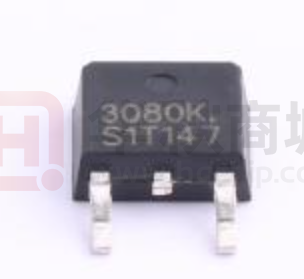


 工商网监
湘ICP备2023018690号
工商网监
湘ICP备2023018690号
