Wuxi I-CORE Electronics Co., Ltd.
rev:B3
Number:AiP74LVC2G125-AX-LJ-B038EN
e
Tab: 835-12
or
AiP74LVC2G125
Dual Buffer/Line Driver; 3-state
Specification
i-c
Product
Specification Revision History:
Version
Date
2017-05-A1
2021-12-A2
2017-05
2021-12
2022-02-A3
2022-02
2022-03-A4
2022-03
Description
New
Modify ordering information
Modify ambient temperature to -40℃~+105℃ and add electrical
characteristics of -40℃~+105℃
Modify ordering information note 1
Address:Building B4,NO.777,Jianzhu Road,Binhu District,Wuxi City,Jiangsu Province
http://www.i-core. cn
P.C.:214072
1/ 13
VER:2022-03-A4
�Wuxi I-CORE Electronics Co., Ltd.
Tab: 835-12
rev:B3
Number:AiP74LVC2G125-AX-LJ-B038EN
1、General Description
The AiP74LVC2G125 provides a dual non-inverting buffer/line driver with 3-state output. The 3-state
—
—
output is controlled by the output enable input (pin nOE). A HIGH-level at pin nOE causes the output to
assume a high-impedance OFF-state.
Inputs can be driven from either 3.3V or 5V devices. This feature allows the use of these devices as
translators in a mixed 3.3V and 5V environment.
This device is fully specified for partial power-down applications using IOFF. The IOFF circuitry disables the
output, preventing a damaging backflow current through the device when it is powered down.
or
e
Features:
Wide supply voltage range from 1.65V to 5.5V
5V tolerant input/output for interfacing with 5V logic
±24mA output drive (VCC=3.0V)
CMOS low power consumption
Latch-up performance exceeds 250mA
Direct interface with TTL levels
Inputs accept voltages up to 5V
Specified from -40℃ to +105℃
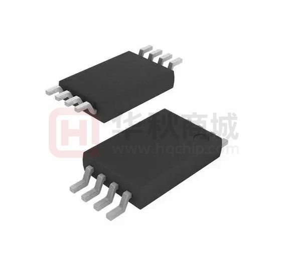
Packaging information: TSSOP8/VSSOP8
Ordering Information:
Reel packing specifications:
Packaging
form
Marking
code
Reel
quantity
i-c
Part number
AiP74LVC2G125TA8.TR
TSSOP8
BRXX
3000
PCS/reel
AiP74LVC2G125YA8.TR
VSSOP8
BRXX
3000
PCS/reel
Boxed reel
quantity
3000
PCS/box
3000
PCS/box
Notes
Dimensions of plastic
enclosure:
3.0mm×3.0mm
Pin spacing: 0.65mm
Dimensions of plastic
enclosure:
2.0mm×2.3mm
Pin spacing: 0.50mm
Note 1: “XX” refers to variable content, meaning year and package batch serial number.
Note 2: If the physical information is inconsistent with the ordering information, please refer to the actual
product.
Address:Building B4,NO.777,Jianzhu Road,Binhu District,Wuxi City,Jiangsu Province
http://www.i-core. cn
P.C.:214072
2/ 13
VER:2022-03-A4
�Wuxi I-CORE Electronics Co., Ltd.
Tab: 835-12
rev:B3
Number:AiP74LVC2G125-AX-LJ-B038EN
2、Block Diagram And Pin Description
2.1、Block Diagram
or
e
Figure 1. Logic symbol
Figure 2. IEC logic symbol
i-c
2.2、Pin Configurations
2.3、Pin Description
Pin No.
Pin Name
—
Description
1
1OE
output enable input (active LOW)
2
3
4
5
6
1A
2Y
GND
2A
1Y
data input
data output
ground (0V)
data input
data output
7
2OE
output enable input (active LOW)
8
VCC
supply voltage
—
Address:Building B4,NO.777,Jianzhu Road,Binhu District,Wuxi City,Jiangsu Province
http://www.i-core. cn
P.C.:214072
3/ 13
VER:2022-03-A4
�Wuxi I-CORE Electronics Co., Ltd.
Tab: 835-12
rev:B3
Number:AiP74LVC2G125-AX-LJ-B038EN
2.4、Function Table
Input
Output
—
nA
nOE
nY
L
L
L
L
H
H
H
X
Z
Note: H=HIGH voltage level; L=LOW voltage level; X=don’t care; Z=high-impedance OFF-state.
3、Electrical Parameter
3.1、Absolute Maximum Ratings
(Voltages are referenced to GND(ground=0V), unless otherwise specified.)
Symbol
VCC
output voltage
VO
IIK
VI
Min.
-0.5
Max.
+6.5
Unit
V
VI < 0V
-50
-
mA
-
-0.5
+6.5
V
VO > VCC or VO < 0V
-
±50
mA
Enable mode
Disable mode
Power-down mode; VCC=0V
VO=0V to VCC
-
-0.5
-0.5
-0.5
-100
VCC+0.5
+6.5
+6.5
±50
100
-
V
V
V
mA
mA
mA
or
IOK
Conditions
-
e
Parameter
supply voltage
input clamping
current
input voltage
Output clamping
current
i-c
output current
IO
supply current
ICC
ground current
IGND
storage
Tstg
-65
+150
temperature
total power
Ptot
300
dissipation
Soldering
TL
10s
250
temperature
Note:
[1] For TSSOP8 package: above 55℃ the value of Ptot derates linearly with 2.5mW/K.
[2] For VSSOP8 package: above 110℃ the value of Ptot derates linearly at 8mW/K.
℃
mW
℃
3.2、Recommended Operating Conditions
Parameter
supply voltage
input voltage
Symbol
VCC
VI
output voltage
VO
ambient
temperature
input transition
rise and fall rate
Conditions
VCC=1.65V to 5.5V; Enable mode
VCC=1.65V to 5.5V; Disable mode
VCC=0V; Power-down mode
Min.
1.65
0
0
0
0
Typ.
-
Max.
5.5
5.5
VCC
5.5
5.5
Unit
V
V
V
V
V
Tamb
-
-40
-
+105
℃
Δt/ΔV
VCC=1.65V to 2.7V
VCC=2.7V to 5.5V
-
-
20
10
ns/V
ns/V
Address:Building B4,NO.777,Jianzhu Road,Binhu District,Wuxi City,Jiangsu Province
http://www.i-core. cn
P.C.:214072
4/ 13
VER:2022-03-A4
�Wuxi I-CORE Electronics Co., Ltd.
Tab: 835-12
rev:B3
Number:AiP74LVC2G125-AX-LJ-B038EN
Unit
V
V
V
V
V
V
V
e
3.3、Electrical Characteristics
3.3.1、DC Characteristics 1
(Tamb=-40℃ to +85℃, voltages are referenced to GND (ground=0V), unless otherwise specified.)
Parameter
Symbol
Conditions
Min. Typ. Max.
0.65×
VCC=1.65V to 1.95V
VCC
VCC=2.3V to 2.7V
1.7
HIGH-level
VIH
input voltage
VCC=2.7V to 3.6V
2.0
0.7×
VCC=4.5V to 5.5V
VCC
0.35×
VCC=1.65V to 1.95V
VCC
V
=2.3V
to
2.7V
0.7
LOW-level
CC
VIL
input voltage
VCC=2.7V to 3.6V
0.8
0.3×
VCC=4.5V to 5.5V
VCC
IO=-100uA;
VCCVCC=1.65V to 5.5V
0.1
IO=-4mA; VCC=1.65V
1.2
HIGH-level
IO=-8mA; VCC=2.3V
1.9
VOH
VI = VIH or VIL
output voltage
IO=-12mA; VCC=2.7V
2.2
IO=-24mA; VCC=3.0V
2.3
IO=-32mA; VCC=4.5V
3.8
IO=100uA;
0.10
VCC=1.65V to 5.5V
IO=4mA; VCC=1.65V
0.45
LOW-level
IO=8mA; VCC=2.3V
0.30
VOL
VI = VIH or VIL
output voltage
IO=12mA; VCC=2.7V
0.40
IO=24mA; VCC=3.0V
0.55
IO=32mA; VCC=4.5V
0.55
input leakage
VI=5.5V or GND;
II
±0.1
±1
current
VCC=0V to 5.5V
OFF-state
VI=VIH or VIL;
IOZ
±0.1
±2
output current
VO=5.5V or GND; VCC=3.6V
power-off
IOFF
VI or VO=5.5V; VCC=0V
±0.1
±2
leakage current
VI=5.5V or GND;
supply current
ICC
0.1
4
VCC=1.65V to 5.5V; IO=0A
additional
per pin; VI=VCC-0.6V;
ΔICC
5
500
supply current
IO=0A; VCC=2.3V to 5.5V
input
CI
2
capacitance
Note: All typical values are measured at VCC=3.3V and Tamb=25℃.
V
V
i-c
or
V
V
V
V
V
Address:Building B4,NO.777,Jianzhu Road,Binhu District,Wuxi City,Jiangsu Province
http://www.i-core. cn
P.C.:214072
V
V
V
V
V
V
uA
uA
uA
uA
uA
pF
5/ 13
VER:2022-03-A4
�Wuxi I-CORE Electronics Co., Ltd.
Tab: 835-12
rev:B3
Number:AiP74LVC2G125-AX-LJ-B038EN
Unit
V
V
V
V
V
V
V
V
e
3.3.2、DC Characteristics 2
(Tamb=-40℃ to +105℃, voltages are referenced to GND (ground=0V), unless otherwise specified.)
Parameter
Symbol
Conditions
Min. Typ. Max.
0.65×
VCC=1.65V to 1.95V
VCC
VCC=2.3V to 2.7V
1.7
HIGH-level
VIH
input voltage
VCC=2.7V to 3.6V
2.0
0.7×
VCC=4.5V to 5.5V
VCC
0.35×
VCC=1.65V to 1.95V
VCC
VCC=2.3V to 2.7V
0.7
LOW-level
VIL
input voltage
VCC=2.7V to 3.6V
0.8
0.3×
VCC=4.5V to 5.5V
VCC
IO=-100uA;
VCCVCC=1.65V to 5.5V
0.1
IO=-4mA; VCC=1.65V
0.95
HIGH-level
IO=-8mA; VCC=2.3V
1.7
VOH
VI = VIH or VIL
output voltage
IO=-12mA; VCC=2.7V
1.9
IO=-24mA; VCC=3.0V
2.0
IO=-32mA; VCC=4.5V
3.4
IO=100uA;
0.10
VCC=1.65V to 5.5V
IO=4mA; VCC=1.65V
0.70
LOW-level
IO=8mA; VCC=2.3V
0.45
VOL
VI = VIH or VIL
output voltage
IO=12mA; VCC=2.7V
0.60
IO=24mA; VCC=3.0V
0.80
IO=32mA; VCC=4.5V
0.80
input leakage
VI=5.5V or GND;
II
±1
current
VCC=0V to 5.5V
OFF-state
VI=VIH or VIL;
IOZ
±2
output current
VO=5.5V or GND; VCC=3.6V
power-off
IOFF
VI or VO=5.5V; VCC=0V
±2
leakage current
VI=5.5V or GND;
supply current
ICC
4
VCC=1.65V to 5.5V; IO=0A
additional
per pin; VI=VCC-0.6V;
ΔICC
500
supply current
IO=0A; VCC=2.3V to 5.5V
Note: All typical values are measured at VCC=3.3V and Tamb=25℃.
V
i-c
or
V
V
V
V
V
Address:Building B4,NO.777,Jianzhu Road,Binhu District,Wuxi City,Jiangsu Province
http://www.i-core. cn
P.C.:214072
V
V
V
V
V
V
uA
uA
uA
uA
uA
6/ 13
VER:2022-03-A4
�Wuxi I-CORE Electronics Co., Ltd.
Tab: 835-12
rev:B3
Number:AiP74LVC2G125-AX-LJ-B038EN
Unit
ns
ns
ns
ns
ns
ns
ns
ns
ns
ns
ns
ns
ns
ns
ns
pF
pF
i-c
or
e
3.3.3、AC Characteristics 1
(Tamb=-40℃ to +85℃, voltages are referenced to GND (ground=0V), unless otherwise specified.)
Parameter
Symbol
Conditions
Min. Typ. Max.
VCC=1.65V to 1.95V
1.0
3.7
9.1
VCC=2.3V to 2.7V
0.5
2.5
4.8
nA to nY
propagation
tpd
see Figure 4
VCC=2.7V
1.0
2.7
4.8
delay
VCC=3.0V to 3.6V
0.5
2.3
4.3
VCC=4.5V to 5.5V
0.5
1.9
3.7
VCC=1.65V to 1.95V
1.5
4.3
9.9
VCC=2.3V to 2.7V
1.0
2.8
5.6
—
nOE to nY
ten
see Figure 5
VCC=2.7V
1.5
3.3
5.7
enable time
VCC=3.0V to 3.6V
0.5
2.4
4.7
VCC=4.5V to 5.5V
0.5
2.0
3.8
VCC=1.65V to 1.95V
1.0
3.5
11.6
V
=2.3V
to
2.7V
0.5
1.8
5.8
—
CC
nOE to nY
tdis
see Figure 5
VCC=2.7V
1.0
2.7
4.8
disable time
VCC=3.0V to 3.6V
1.0
2.7
4.6
VCC=4.5V to 5.5V
0.5
1.8
3.4
Power
per buffer;
output enabled
18
dissipation
CPD
VI= GND to
output disabled
5
capacitance
VCC
Note:
[1] Typical values are measured at nominal VCC and at Tamb=25℃.
[2] tpd is the same as tPLH and tPHL.
[3] ten is the same as tPZH and tPZL.
[4] tdis is the same as tPLZ and tPHZ.
[3] CPD is used to determine the dynamic power dissipation (PD in uW).
PD=(CPD×VCC2×fi×N)+∑(CL×VCC2×fo) where:
fi=input frequency in MHz;
fo=output frequency in MHz;
CL=output load capacitance in pF;
VCC=supply voltage in V;
N=number of inputs switching;
∑(CL×VCC2×fo)=sum of outputs.
Address:Building B4,NO.777,Jianzhu Road,Binhu District,Wuxi City,Jiangsu Province
http://www.i-core. cn
P.C.:214072
7/ 13
VER:2022-03-A4
�Wuxi I-CORE Electronics Co., Ltd.
Tab: 835-12
rev:B3
Number:AiP74LVC2G125-AX-LJ-B038EN
Unit
ns
ns
ns
ns
ns
ns
ns
ns
ns
ns
ns
ns
ns
ns
ns
i-c
or
e
3.3.4、AC Characteristics 2
(Tamb=-40℃ to +105℃, voltages are referenced to GND (ground=0V), unless otherwise specified.)
Parameter
Symbol
Conditions
Min. Typ. Max.
VCC=1.65V to 1.95V
1.0
11.4
VCC=2.3V to 2.7V
0.5
6.0
nA to nY
propagation
tpd
see Figure 4
VCC=2.7V
1.0
6.0
delay
VCC=3.0V to 3.6V
0.5
5.5
VCC=4.5V to 5.5V
0.5
4.6
VCC=1.65V to 1.95V
1.5
12.4
VCC=2.3V to 2.7V
1.0
7.0
—
nOE to nY
ten
see Figure 5
VCC=2.7V
1.5
7.1
enable time
VCC=3.0V to 3.6V
0.5
5.9
VCC=4.5V to 5.5V
0.5
4.8
VCC=1.65V to 1.95V
1.0
14.1
V
=2.3V
to
2.7V
0.5
7.6
—
CC
nOE to nY
tdis
see Figure 5
VCC=2.7V
1.0
6.2
disable time
VCC=3.0V to 3.6V
1.0
5.9
VCC=4.5V to 5.5V
0.5
4.6
Note:
[1] Typical values are measured at nominal VCC and at Tamb=25℃.
[2] tpd is the same as tPLH and tPHL.
[3] ten is the same as tPZH and tPZL.
[4] tdis is the same as tPLZ and tPHZ.
Address:Building B4,NO.777,Jianzhu Road,Binhu District,Wuxi City,Jiangsu Province
http://www.i-core. cn
P.C.:214072
8/ 13
VER:2022-03-A4
�Wuxi I-CORE Electronics Co., Ltd.
Tab: 835-12
rev:B3
Number:AiP74LVC2G125-AX-LJ-B038EN
4、Testing Circuit
or
e
4.1、AC Testing Circuit
Figure 3. Test circuit for measuring switching times
i-c
Definitions for test circuit:
RL=Load resistance.
CL=Load capacitance including jig and probe capacitance.
RT=Termination resistance; should be equal to the output impedance Zo of the pulse generator.
VEXT=External voltage for measuring switching times.
4.2、AC Testing Waveforms
Figure 4. The input (nA) to output (nY) propagation delay times
Address:Building B4,NO.777,Jianzhu Road,Binhu District,Wuxi City,Jiangsu Province
http://www.i-core. cn
P.C.:214072
9/ 13
VER:2022-03-A4
�Wuxi I-CORE Electronics Co., Ltd.
rev:B3
Number:AiP74LVC2G125-AX-LJ-B038EN
e
Tab: 835-12
or
Figure 5. 3-state enable and disable times
Input
Output
VM
0.5×VCC
0.5×VCC
1.5V
1.5V
0.5×VCC
VM
0.5×VCC
0.5×VCC
1.5V
1.5V
0.5×VCC
i-c
4.3、Measurement Points
Supply voltage
VCC
1.65V to 1.95V
2.3V to 2.7V
2.7V
3.0V to 3.6V
4.5V to 5.5V
4.4、Test Data
Supply voltage
Input
VX
VOL+0.15V
VOL+0.15V
VOL+0.3V
VOL+0.3V
VOL+0.3V
Load
VCC
VI
tr = tf
CL
RL
1.65V to 1.95V
2.3V to 2.7V
2.7V
3.0V to 3.6V
4.5V to 5.5V
VCC
VCC
2.7V
2.7V
VCC
≤ 2.0ns
≤ 2.0ns
≤ 2.5ns
≤ 2.5ns
≤ 2.5ns
30pF
30pF
50pF
50pF
50pF
1kΩ
500Ω
500Ω
500Ω
500Ω
tPLH,
tPHL
open
open
open
open
open
Address:Building B4,NO.777,Jianzhu Road,Binhu District,Wuxi City,Jiangsu Province
http://www.i-core. cn
P.C.:214072
VY
VOH-0.15V
VOH-0.15V
VOH-0.3V
VOH-0.3V
VOH-0.3V
VEXT
tPZH,
tPHZ
GND
GND
GND
GND
GND
tPZL,
tPLZ
2×VCC
2×VCC
6V
6V
2×VCC
10/ 13
VER:2022-03-A4
�Wuxi I-CORE Electronics Co., Ltd.
Tab: 835-12
rev:B3
Number:AiP74LVC2G125-AX-LJ-B038EN
5、Package Information
i-c
or
e
5.1、TSSOP8
Address:Building B4,NO.777,Jianzhu Road,Binhu District,Wuxi City,Jiangsu Province
http://www.i-core. cn
P.C.:214072
11/ 13
VER:2022-03-A4
�Wuxi I-CORE Electronics Co., Ltd.
Tab: 835-12
rev:B3
Number:AiP74LVC2G125-AX-LJ-B038EN
i-c
or
e
5.2、VSSOP8
Address:Building B4,NO.777,Jianzhu Road,Binhu District,Wuxi City,Jiangsu Province
http://www.i-core. cn
P.C.:214072
12/ 13
VER:2022-03-A4
�Wuxi I-CORE Electronics Co., Ltd.
Tab: 835-12
rev:B3
Number:AiP74LVC2G125-AX-LJ-B038EN
6、Statements And Notes
6.1、The name and content of Hazardous substances or Elements in the product
Hazardous substances or Elements
Part name
Lead
and
lead
compo
unds
Mercur
y and
mercur
y
compo
unds
Cadm
ium
and
cadmi
um
comp
ounds
Hexaval
ent
chromiu
m
compoun
ds
Polybro
minated
biphenyl
s
Polybro
minate
d
biphen
yl
ethers
Dibutyl
phthala
te
Butylbe
nzyl
phthala
te
Di-2-et
hylhex
yl
phthala
te
Diisobu
tyl
phthala
te
○
○
○
○
○
○
○
○
○
○
Plastic resin
○
○
○
○
○
○
○
○
○
○
Chip
○
○
○
○
○
○
○
○
○
○
The lead
○
○
○
○
○
○
○
○
○
○
Plastic sheet
installed
○
○
○
e
Lead frame
○
○
○
○
○
○
○
○:Indicates that the content of hazardous substances or elements in the detection limit
of
the following the SJ/T11363-2006 standard.
×:Indicates that the content of hazardous substances or elements exceeding the SJ/T11363-2006
Standard limit requirements.
or
explanation
6.2、Notion
Recommended carefully reading this information before the use of this product;
The information in this document are subject to change without notice;
i-c
This information is using to the reference only, the company is not responsible for any loss;
The company is not responsible for the any infringement of the third party patents or other rights of
the responsibility.
Address:Building B4,NO.777,Jianzhu Road,Binhu District,Wuxi City,Jiangsu Province
http://www.i-core. cn
P.C.:214072
13/ 13
VER:2022-03-A4
�


 工商网监
湘ICP备2023018690号
工商网监
湘ICP备2023018690号
