SM3416
N-Channel Enhancement-Mode MOSFET (20V,6.5A)
PRODUCT SUMMARY
VDSS
20V
ID
6.5A
RDS(on) (m-ohm) Max
22 @ VGS = 4.5V, ID=6.5A
26 @ VGS = 2.5V, ID=5.5A
34 @ VGS = 1.8V, ID=5.0A
◆ Features
The SM3416 uses advanced trench technology to provide excellent RDS(ON), low gate charge
and operation with gate voltages as low as 1.8V. This device is suitable for use as a load switch or in
PWM applications. It is ESD(2000V HBM) protected.
SM3416 Pin Assignment & Symbol
3-Lead Plastic SOT-23-3L
Pin1:
:Gate 2:Source 3:Drain
◆ Ordering Information
Ordering Number
Lead Free
Halogen Free
SM3416LRL
SM3416LRG
Pin Assignment
Package
1
G
SOT-23-3L
SM3416-LR-G
(1) L:SOT-23-3L
(1)Package Type
(2) R:Tape Reel
(2)Packing Type
3
D
Packing
Tape Reel
(3) G:Halogen Free;L:Lead Free
(3)Lead Free
V01
2
S
1
www.sourcechips.com
�SM3416
◆ Absolute Maximum Ratings (TA=25oC, unless otherwise noted)
Symbol
Ratings
Units
VDS
Drain-Source Voltage
20
V
VGS
Gate-Source Voltage
±8
V
TA=25°C
6.5
TA=75°C
5.2
ID
Continuous Drain Current
IDM
Drain Current (Pulsed)
PD
Power Dissipation
IS
Maximum Body-Diode Continuous Current
Tj, Tstg
Note
Parameter
a
A
30
TA=25°C
1.4
TA=75°C
0.9
Operating Junction and Storage Temperature Range
b
:a. Repetitive Rating: Pulse width limited by the maximum junction temperature
A
W
1
A
-55 to +150
°C
b.1-in2 2oz Cu PCB board
◆ Electrical Characteristics (TA=25°C, unless otherwise noted)
Symbol
Characteristic
• Off Characteristics
BVDSS
Drain-Source Breakdown Voltage
IDSS
Zero Gate Voltage Drain Current
IGSS
Gate-Body Leakage Current
• On Characteristicsc
VGS(th)
Gate Threshold Voltage
Test Conditions
VGS=0V, ID=250uA
VDS=20V, VGS=0V
VGS=±8V, VDS=0V
VDS=VGS, ID=250uA
VGS=4.5V, ID=6.5A
Drain-Source On-State Resistance
VGS=2.5V, ID=5.5A
RDS(on)
VGS=1.8V, ID=5.0A
gFS
Forward Transconductance
VDS=5 V, ID=6.5A
VSD
Diode Forward Voltage
IS=1A,VGS=0V
IS
Maximum Body-Diode Continuous Current
• Dynamic Characteristics d
Ciss
Input Capacitance
VDS=10 VGS=0V, f=1MHz
Coss
Output Capacitance
Crss
Reverse Transfer Capacitance
• Switching Characteristicsd
Qg
Total Gate Charge
VDS=10V ID=6.5 VGS=4.5V
Qgs
Gate-Source Charge
Qgd
Gate-Drain Charge
td(on)
Turn-on Delay Time
VDD = 10V, RL = 1.5Ω
tr
Turn-on Rise Time
ID = 1A, VGEN = 5V
td(off)
Turn-off Delay Time
RG = 3Ω
tf
Turn-off Fall Time
• Drain-Source Diode Characteristics
VSD
Drain-Source Diode Forward Voltage VGS=0V, IS=1A
,
,
c.Pulse Test : Pulse Width < 300μs, Duty Cycle < 2%.
d.Guaranteed by design, not subject to production testing.
V01
2
www.sourcechips.com
Min.
Typ.
Max.
Unit
20
-
-
1
±10
V
uA
uA
V
-
50
0.7
-
1
22
26
34
1
1
-
1160
104
29
-
-
10
1.4
2.7
6.2
12.7
51.7
16
-
-
0.7
1.2
0.4
-
mΩ
S
V
A
pF
nC
nS
V
�SM3416
◆ Characteristics Curve(
(Ta=25℃
℃,unless otherwise note)
)
V01
3
www.sourcechips.com
�SM3416
◆ Characteristics Curve(
(Ta=25℃
℃,unless otherwise note)
)
V01
4
www.sourcechips.com
�SM3416
◆ Characteristics Curve(
(Ta=25℃
℃,unless otherwise note)
)
V01
5
www.sourcechips.com
�
很抱歉,暂时无法提供与“SM3416SRL”相匹配的价格&库存,您可以联系我们找货
免费人工找货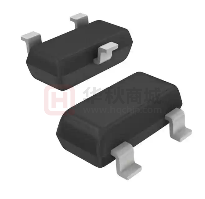


 工商网监
湘ICP备2023018690号
工商网监
湘ICP备2023018690号

