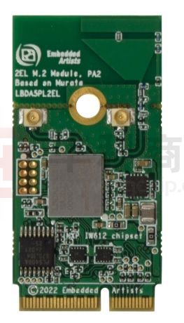
2EL M.2 Module - Datasheet
Document status: Preliminary
Copyright 2023 © Embedded Artists AB
2EL M.2 Module Datasheet
(EAR00409 / EAR00463 / EAR00464)
Get Up-and-Running Quickly and
Start Developing Your Application On Day 1!
�2EL M.2 Module - Datasheet
Page 2
Embedded Artists AB
Rundelsgatan 14
211 36 Malmö
Sweden
https://www.EmbeddedArtists.com
Copyright 2023 © Embedded Artists AB. All rights reserved.
No part of this publication may be reproduced, transmitted, transcribed, stored in a retrieval system, or
translated into any language or computer language, in any form or by any means, electronic,
mechanical, magnetic, optical, chemical, manual or otherwise, without the prior written permission of
Embedded Artists AB.
Disclaimer
Embedded Artists AB makes no representation or warranties with respect to the contents hereof and
specifically disclaim any implied warranties or merchantability or fitness for any particular purpose. The
information has been carefully checked and is believed to be accurate, however, no responsibility is
assumed for inaccuracies.
Information in this publication is subject to change without notice and does not represent a
commitment on the part of Embedded Artists AB.
Feedback
We appreciate any feedback you may have for improvements on this document.
Trademarks
All brand and product names mentioned herein are trademarks, services marks, registered
trademarks, or registered service marks of their respective owners and should be treated as such.
Copyright 2022 © Embedded Artists AB
�2EL M.2 Module - Datasheet
Page 3
Table of Contents
1 Document Information
4
1.1
4
Revision History
2 Introduction
5
2.1
Benefits of Using an M.2 Module to get Wireless Connectivity
5
2.2
More M.2 Related Information
5
2.3
ESD Precaution and Handling
6
2.4
Product Compliance
6
3 Specification
7
3.1
Power Up Sequence
8
3.2
External Sleep Clock
8
3.3
Mechanical Dimensions
9
3.4
M.2 Pinning
11
3.5
On-board I2C GPIO Expander
15
3.6
Block Diagram
15
3.7
IEEE802.15.4 Interface
16
3.8
SDIO Interface
16
3.9
Wi-Fi Interface Control
17
3.10
Test Points and Expansion Header
18
3.11
Current Consumption Measurements
20
4 Versions of 2EL Module
21
5 Antenna
22
5.1
Mounting and Clearance
22
5.2
Antenna Connector
22
5.3
Overriding on-board PCB Trace Antenna
23
5.4
On-board PCB Trace Antenna Performance
24
6 Software and Support
6.1
Software Driver
27
6.2
Support
28
7 Regulatory
29
7.1
European Union Regulatory Compliance
8 Disclaimers
8.1
Copyright 2022 © Embedded Artists AB
27
Definition of Document Status
29
30
31
�2EL M.2 Module - Datasheet
1
Page 4
Document Information
This document applies to the following products.
Product Name
Type Number
Murata Module
Chipset
Product Status
2EL M.2 Module,
rev PA2/A/A1
EAR00409 / EAR00463 /
EAR00464
LBES5PL2EL-923
NXP IW612
Initial Production
This table below lists the product differences. All products are not stocked. Consult Embedded Artists
for availability and lead time.
Type
Number
Product Name
Antenna
Packaging
EAR00409
2EL M.2 Module
On-board antenna
Individual packing for evaluation
EAR00463
2EL M.2 Module
On-board antenna
Tray packing
EAR00464
2EL M.2 Module
External antenna
via u.fl.connectors
Tray packing
1.1 Revision History
Revision
Date
Description
PA1
2022-07-01
First version.
PA2
2023-03-03
Added information about orderable products.
Copyright 2022 © Embedded Artists AB
�2EL M.2 Module - Datasheet
Page 5
2 Introduction
This document is a datasheet that specifies and describes the 2EL M.2 module mainly from a
hardware point of view.
The main component in the design is Murata's 2EL module (full part number: LBES5PL2EL), which in
turn is based on the NXP IW612 chipset. The 2EL module enable Wi-Fi, Bluetooth, Bluetooth Low
Energy (LE) and IEEE802.15.4 communication.
There are multiple application areas for the 2EL M.2 Module:
•
•
•
•
Industrial and Buildings automation
Asset management
IoT applications
Smart home: Voice assist device, smart printer, smart speaker, home automation gateway,
and IP camera
Retail/POS
Healthcare and medical devices
Smart city
and many more…
•
•
•
•
2.1
Benefits of Using an M.2 Module to get Wireless Connectivity
There are several benefits to use an M.2 module to add connectivity to an embedded design:
•
•
Drop-in, certified solution!
Modular and flexible approach to evaluate different Wi-Fi/BT solutions - with different tradeoffs around performance, cost, power consumption, longevity, etc.
Access to maintained software drivers (Linux and SDK) with responsive support from Murata.
Supported by Embedded Artists' Developer's Kits for i.MX 8/9 development, including
advanced debugging support on carrier boards
One component to buy, instead of 40+
No RF expertise is required
Developed in close collaboration with Murata
•
•
•
•
•
2.2
More M.2 Related Information
For more information about the M.2 standard and Embedded Artists' adaptation, see: M.2 Primer
For more general information about the M.2 standard, see: https://en.wikipedia.org/wiki/M.2
The official M.2 specification (PCI Express M.2 Specification) is available from: www.pcisig.com
Copyright 2022 © Embedded Artists AB
�2EL M.2 Module - Datasheet
2.3
Page 6
ESD Precaution and Handling
Please note that the M.2 module come without any case/box and all
components are exposed for finger touches – and therefore extra attention must
be paid to ESD (electrostatic discharge) precaution, for example use of staticfree workstation and grounding strap. Only qualified personnel shall handle the
product.
Make it a habit always to first touch the mounting hole (which is grounded)
for a few seconds with both hands before touching any other parts of the
boards. That way, you will have the same potential as the board and therefore minimize the risk for
ESD.
In general touch as little as possible on the boards in order to minimize the risk of ESD damage. The
only reasons to touch the board are when mounting/unmounting it on a carrier board.
Note that Embedded Artists does not replace modules that have been damaged by ESD.
2.4
Product Compliance
Visit Embedded Artists' website at http://www.embeddedartists.com/product_compliance for up-to-date
information about product compliances such as CE, UKCA, RoHS2/3, Conflict Minerals, REACH, etc.
Copyright 2022 © Embedded Artists AB
�2EL M.2 Module - Datasheet
Page 7
3 Specification
This chapter lists some of the more important characteristics of the M.2 module, but it is not a full
specification of performance and timing. The main component in the design is NXP's 2EL module (full
part number: LBES5PL2EL), which in turn is based around NXP's IW612 chipset.
For a detailed specification, see the LBES5PL2EL product page at Murata:
https://www.murata.com/products/connectivitymodule/wi-fi-bluetooth/overview/lineup/type2el
For a full specification, see Murata's 2EL Module (LBES5PL2EL) product page:
https://www.murata.com/products/productdata/8819414302750/TYPE2EL.pdf
Module / Chipset
Murata module
LBES5PL2EL-923
Chipset
NXP IW612
Wi-Fi
Standards
802.11a/b/g/n/ac/ax SISO, Wi-Fi 6
Network
uAP and STA dual mode
Frequency
2.4GHz and 5 GHz band
Data rates
601 Mbps
Host interface
SDIO 3.0, SDR12@24MHz, SDR25@50MHz, SDR50@100MHz,
DDR50@50MHz
Bluetooth
Standards
5.3 BR/EDR/LE, 2Mbps PHY
Power Class
Class 1.5
Host interface
4-wire UART@4MBaud
Audio interface
PCM for audio
IEEE802.15.4
Standards
IEEE 802.15.4-2015 compliant supporting Thread in 2.4 GHz band
PA
Integrated high power PA up to +20 dBm transmit power
Host interface
SPI
Powering
Operating conditions on supply voltage to M.2 module
Min
Typ
Max
0.0V minimum
3.3V
3.15V operating and
RF specification
3.46V
Absolute maximum rating on supply voltage to M.2 module
Min
Max
Note: Do not exceed minimum or maximum voltage.
Module will be permanently damaged above this limit!
0.0V
3.63V
Copyright 2022 © Embedded Artists AB
�2EL M.2 Module - Datasheet
Page 8
Peak current
1050 mA max
The power supply must be designed for
this peak current, which typically happen
during the startup calibration process.
Receive mode current (WLAN)
TBD mA typical max
Note that current consumption varies
widely between different operational
modes.
Transmit mode current (WLAN)
TBD mA typical max
Note that current consumption varies
widely between different operational
modes.
Environmental Specification
Operational Temperature
-40 to +85 degrees Celsius
Storage Temperature
-40 to +85 degrees Celsius
Relative Humidity (RH),
operating and storage
10 - 90% non-condensing
3.1
Power Up Sequence
The supply voltage shall not rise (10 - 90%) faster than 40 microseconds and not slower than 100
milliseconds.
Chipset signals PD_N (M.2 signal W_DISABLE1#) must be held low for at least 1 milliseconds after
supply voltage has reached specification level before pulled high.
3.2
External Sleep Clock
The sleep clock signals can be applied to a powered and unpowered M.2 module.
Clock Specification
Frequency
32.768 kHz
Frequency accuracy
±205 ppm including initial tolerance, aging, temperature, etc.
Duty cycle
20 - 80%
Phase noise requirement
-125 dBc/Hz typical (measured at 100kHz)
Clock jitter
1.5 ns typical (RMS)
Voltage level
3.3V logic, according to M.2 standard
Copyright 2022 © Embedded Artists AB
�2EL M.2 Module - Datasheet
3.3
Page 9
Mechanical Dimensions
The M.2 module is of type: 2230-D5-E according to the M.2 nomenclature. This means width 22 mm,
length 30mm (without trace antenna), top and bottom side component height 1.5 mm and key-E
connector. The table below lists the different dimensions and weight.
M.2 Module Dimension
Value (±0.15 mm)
Unit
Width
22
mm
Height, with pcb trace antenna
Height, without pcb trace antenna
44
30
mm
mm
PCB thickness
0.8
mm
Maximum component height on top side
1.5
mm
Maximum component height on bottom side
1.5
mm
Ground hole diameter
3.5
mm
Plating around ground hole, diameter
5.5
mm
Module weight
1.5 ±0.5 gram
gram
Embedded Artists has added a non-standard feature to the 2230 M.2 modules designed together with
Murata, NXP and Infineon (former Cypress). The pictures below illustrate the how the standard module
size has been extended by 14 mm in the length direction to include a pcb trace antenna.
44 mm
30 mm
Standard size:
22 x 30 mm
Non-standard size:
22 x 44 mm
with pcb trace
antenna
22 mm
Figure 1 – M.2 Module with, and without, PCB Trace Antenna
Copyright 2022 © Embedded Artists AB
22 mm
�2EL M.2 Module - Datasheet
Page 10
The picture below gives dimensions for the grounded center (half) hole and the u.fl. antenna
connector.
11 mm,
centered
8.0 mm
4.9 mm
1.5 mm
Figure 2 – M.2 Module Without Trace Antenna
Copyright 2022 © Embedded Artists AB
�2EL M.2 Module - Datasheet
3.4
Page 11
M.2 Pinning
This section presents the pinning used for the M.2 module. It is essentially M.2 Key-E compliant with
extensions to support the IEEE802.15.4 functionality. The pin assignment for specific control has been
jointly defined by Embedded Artists, Murata, NXP and Infineon (former Cypress).
The picture below illustrates the edge pin numbering. It starts on the right edge and alternates between
top and bottom side. The removed pads in the keying notch count (but are obviously non-existing).
Pin 75 on top side
Pin 1 on top side
Pin 74 on bottom side
Pin 2 on bottom side
Figure 3 – M.2 Module Pin Numbering
The Wi-Fi interface use the SDIO interface. The Bluetooth interface use the UART interface for control
and PCM interface for audio. The IEEE802.15.4 interface use a non-standard SPI interface. The table
below lists the pin usage for the 2EL M.2 modules. The column "When is signal needed" signals four
different categories:
•
•
•
•
•
Always: These signals shall always be connected.
Wi-Fi SDIO: These signals shall always be connected then the Wi-Fi interface is used.
Bluetooth: These signals shall always be connected then the Bluetooth interface is used.
IEEE802.15.4: These signals shall always be connected then the IEEE802.15.4 interface is
used.
Optional: These signals are optional to connect.
Pin #
Side
of pcb
M.2 Name
Voltage Level and
Signal Direction
When is
signal needed
Note
1
Top
GND
GND
Always
Connect to ground
2
Bottom
3.3 V
Always
Power supply input. Connect to stable, low-noise 3.3V supply.
3
Top
USB_D+
Copyright 2022 © Embedded Artists AB
Not connected.
�2EL M.2 Module - Datasheet
Page 12
4
Bottom
3.3 V
Always
Power supply input. Connect to stable, low-noise 3.3V supply.
5
Top
USB_D-
Not connected.
6
Bottom
LED_1#
Not connected.
7
Top
GND
GND
Always
Connect to ground.
8
Bottom
PCM_CLK
1.8V I/O
Bluetooth audio
For Bluetooth audio interface: PCM_CLK
Connected to 2EL module, signal GPIO_4, pin 57
9
Top
SDIO CLK
1.8V Input to M.2
Wi-Fi
For Wi-Fi SDIO interface: SDIO_CLK
Connected to 2EL module, signal SD_CLK, pin 44
10
Bottom
PCM_SYNC
1.8V I/O
Bluetooth audio
For Bluetooth audio interface: PCM_SYNC
Connected to 2EL module, signal GPIO_7, pin 61
11
Top
SDIO CMD
1.8V I/O
Wi-Fi
For Wi-Fi SDIO interface: SDIO_CMD
Connected to 2EL module, signal SD_CMD, pin 42
Note: Require an external 10-100K ohm pullup
12
Bottom
PCM_OUT
1.8V output from M.2
Bluetooth audio
For Bluetooth audio interface: PCM_OUT
Connected to 2EL module, signal GPIO_5, pin 59
13
Top
SDIO DATA0
1.8V I/O
Wi-Fi
For Wi-Fi SDIO interface: SDIO_D0
Connected to 2EL module, signal SD_DATA_0, pin 48
Note: Require an external 10-100K ohm pullup
14
Bottom
PCM_IN
1.8V input to M.2
Bluetooth audio
For Bluetooth audio interface: PCM_IN
Connected to 2EL module, signal GPIO_6, pin 60
15
Top
SDIO DATA1
1.8V I/O
Wi-Fi
For Wi-Fi SDIO interface: SDIO_D1
Connected to 2EL module, signal SD_DATA_1, pin 45
Note: Require an external 10-100K ohm pullup
16
Bottom
LED_2#
17
Top
SDIO DATA2
Not connected.
1.8V I/O
Wi-Fi
For Wi-Fi SDIO interface: SDIO_D2
Connected to 2EL module, signal SD_DATA_2, pin 47
Note: Require an external 10-100K ohm pullup
18
Bottom
GND
19
Top
SDIO DATA3
1.8V I/O
Always
Connect to ground.
Wi-Fi
For Wi-Fi SDIO interface: SDIO_D3
Connected to 2EL module, signal SD_DATA_3, pin 46
Note: Require an external 10-100K ohm pullup
20
Bottom
UART WAKE#
3.3V OD output from
M.2
Bluetooth
For Bluetooth UART interface: BT15.4_WAKE_OUT
Connected to 2EL module, via buffer, signal GPIO_19, pin 76
Require an external 10K pullup resistor to 3.3V.
21
Top
SDIO WAKE#
1.8V OD output from
M.2
Wi-Fi
For Wi-Fi SDIO interface: WL_WAKE_OUT
Connected to 2EL module, signal GPIO_17, pin 73
Note: Require an external 10K pullup resistor to 1.8V
22
Bottom
UART TXD
1.8V output from M.2
Bluetooth
For Bluetooth UART interface: UART_TXD
Connected to 2EL module, signal GPIO11, pin 49
23
Top
SDIO RESET#
1.8V input to M.2
Wi-Fi
Independent reset signal for Wi-Fi functionality.
Connected to 2EL module, signal GPIO_1, pin 63.
SDIO RESET#: High = Wi-Fi part of module enabled/internally
powered, Low = Wi-Fi disabled/powered down.
24
Copyright 2022 © Embedded Artists AB
Key, non existing
�2EL M.2 Module - Datasheet
Page 13
25
Key, non existing
26
Key, non existing
27
Key, non existing
28
Key, non existing
29
Key, non existing
30
Key, non existing
31
Key, non existing
32
Bottom
UART_RXD
1.8V input to M.2
Bluetooth
For Bluetooth UART interface: BT_UART_RXD
Connected to 2EL module, signal GPIO_10, pin 51
33
Top
GND
34
Bottom
UART_RTS
1.8V output from M.2
Always
Connect to ground.
Bluetooth
For Bluetooth UART interface: BT_UART_RTS
Connected to 2EL module, signal GPIO_9, pin 52
35
Top
PERp0
36
Bottom
UART_CTS
Not connected.
1.8V input to M.2
Bluetooth
For Bluetooth UART interface: BT_UART_CTS
Connected to 2EL module, signal GPIO_8, pin 50
37
Top
PERn0
38
Bottom
VENDOR
DEFINED
Not connected.
1.8V input to M.2
IEEE802.15.4
SPI_MOSI, the SPI data signal (from host to M.2) for the
IEEE802.15.4/SPI interface.
Connected to 2EL module, via buffer, signal GPIO_14, pin 6.
The buffer is only enabled if bit 0 of the on-board I2C GPIO
expander is set to 1.
39
Top
GND
40
Bottom
VENDOR
DEFINED
1.8V output from M.2
Always
Connect to ground.
IEEE802.15.4
SPI_MISO, the SPI data signal (from M.2 to host) for the
IEEE802.15.4/SPI interface.
Connected to 2EL module, via buffer, signal GPIO_15, pin 7.
The buffer is only enabled if bit 0 of the on-board I2C GPIO
expander is set to 1.
41
Top
PETp0
42
Bottom
VENDOR
DEFINED
Not connected.
1.8V input to M.2
IEEE802.15.4
SPI_SCK, the SPI clock signal (from host to M.2) for the
IEEE802.15.4/SPI interface.
Connected to 2EL module, via buffer, signal GPIO_12, pin 8.
The buffer is only enabled if bit 0 of the on-board I2C GPIO
expander is set to 1.
43
Top
PETn0
44
Bottom
COEX3
Not connected.
1.8V I/O
Optional
Connected to 2EL module, signal GPIO_30, pin 36.
Note: Signal can be JTAG_TDI
45
Top
GND
46
Bottom
COEX_TXD
1.8V I/O
Always
Connect to ground.
Optional
Connected to 2EL module, signal GPIO_28, pin 35.
Note: Signal can be JTAG_TCK
47
Top
REFCLKp0
48
Bottom
COEX_RXD
Not connected.
1.8V I/O
Optional
Connected to 2EL module, signal GPIO_29, pin 34.
Note: Signal can be JTAG_TMS
49
Top
REFCLKn0
50
Bottom
SUSCLK
Not connected.
3.3V input to M.2
Always
External sleep clock input (32.768kHz)
Connected to 2EL module, via buffer, signal SLP_CLK_IN, pin
3
Copyright 2022 © Embedded Artists AB
�2EL M.2 Module - Datasheet
Page 14
51
Top
GND
Always
52
Bottom
PERST0#
Not connected.
53
Top
CLKREQ0#
Not connected.
54
Bottom
W_DISABLE2#
3.3V input to M.2
Always
Connect to ground.
Independent reset signal for Bluetooth functionality.
Connected to 2EL module, via buffer, signal GPIO_2, pin 64.
W_DISABLE#2: High = Bluetooth part of module
enabled/internally powered, Low = Bluetooth disabled/powered
down
55
Top
PEWAKE0#
56
Bottom
W_DISABLE1#
57
Top
GND
58
Bottom
I2C_SDA
59
Top
Reserved
60
Bottom
I2C_CLK
61
Top
Reserved
62
Bottom
ALERT#
Not connected.
3.3V input to M.2
1.8V I/O
Always
Connected to 2EL module, via buffer, signal PD_N, pin 10
W_DISABLE1#: High = The module is enabled/internally
powered, Low = The modules is disabled/powered down
Always
Connect to ground.
Optional /
IEEE802.15.4
I2C data signal, connected to on-board GPIO expander,
PCAL6408A
Not connected.
1.8V input to M.2
Optional /
IEEE802.15.4
I2C clock signal, connected to on-board GPIO expander,
PCAL6408A
Not connected.
1.8V output from M.2
IEEE802.15.4
SPI_INT, interrupt signal from the IEEE802.15.4/SPI interface.
Connected to 2EL module, signal GPIO_20, pin 5
63
Top
GND
64
Bottom
RESERVED
1.8V input to M.2
Always
Connect to ground.
IEEE802.15.4
SPI_SSEL, SPI select signal for the IEEE802.15.4/SPI
interface.
Connected to 2EL module, via buffer, signal GPIO_13, pin 4.
The buffer is only enabled if bit 0 of the on-board I2C GPIO
expander is set to 1.
65
Top
Reserved
Not connected.
66
Bottom
UIM_SWP
Not connected.
67
Top
Reserved
Not connected.
68
Bottom
UIM_POWER_
SNK
Not connected.
69
Top
GND
70
Bottom
UIM_POWER_
SRC/GPIO_1
Not connected.
71
Top
Reserved
Not connected.
72
Bottom
3.3 V
73
Top
Reserved
74
Bottom
3.3 V
Always
Power supply input. Connect to stable, low-noise 3.3V supply.
75
Top
GND
Always
Connect to ground.
Copyright 2022 © Embedded Artists AB
Always
Always
Connect to ground.
Power supply input. Connect to stable, low-noise 3.3V supply.
Not connected.
�2EL M.2 Module - Datasheet
3.5
Page 15
On-board I2C GPIO Expander
The IW612 chipsets needs several control signals and there is a limited number of available pins in the
M.2 standard. In order to create four output signals and one input signal, there is an on-board I2C
GPIO expander, PCAL6408A. It can be accessed at I2C address 0x20 (7-bit address) or 0x40/0x41 (8bit address).
The table below lists the usage the four output signals and one input signal.
Bit Signal Name
Direction
Usage / Connection
0
output
0 = The SPI interface of the IW612 chipset is not
connected to M.2 pins 38, 40, 42, and 64. The SPI
interface can however be accessed via the expansion
header, see section 3.10 for details.
SPI_ENABLE
1= Connect SPI interface of IW612 chipset to M.2 pins
38, 40, 42 and 64.
1
IND_RST_15_4
output
Independent reset signal for IEEE802.15.4
Connects to 2EL module, signal GPIO_24, pin 38
2
IND_WAKE_WLAN
output
Wi-Fi wakeup signal from host to IW612 chipset
WL_WAKE_IN
Connects to 2EL module, signal GPIO_16, pin 74
3
IND_WAKE_BT15_4
output
Bluetooth and IEEE802.15.4 wakeup signal from host to
IW612 chipset
Connects to 2EL module, signal GPIO_18, pin 75
4
RST_IND
input
Reset indication signal (output) from IW612 chipset
Connects to 2EL module, signal GPIO_22, pin 37
3.6
Block Diagram
It can be difficult to understand the internal structure from just ready pin definitions. The block diagram
below explains the structure with blocks instead. One of the I2C-GPIOs is used to control the buffer
then enables/disables the SPI interface.
M.2 I/F
2EL module
SDIO interface
SDIO Wi-Fi interface
Control signals
Control signals
UART interface
UART BL/BLE interface
I2S interface
I2S Audio interface
I2C interface
Vendor defined
& reserved pins
Figure 4 – 2EL M.2 Module Block Diagram
Copyright 2022 © Embedded Artists AB
I2C GPIO
expander
SPI enable
Buffer
Control signals
SPI IEEE802.15.4 interface
�2EL M.2 Module - Datasheet
3.7
Page 16
IEEE802.15.4 Interface
The IW612 chipset also implements an IEEE802.15.4 interface, which is a low-rate wireless personal
area network (LR-WPAN) that was developed for low-data-rate monitor and control applications and
extended-life low-power-consumption uses.
The IEEE802.15.4 functionality is accessed via an SPI interface. There is no standard SPI interface
defined in the M.2 standard, but there are Vendor defined and reserved pins. These are used for the
SPI interface. The 2EL M.2 module has a buffer that connects/disconnects the SPI interface IW612
chipset to the M.2 pins. This buffer is only enabled if bit 0 of the on-board I2C GPIO expander is set to
1.
Besides accessing the SPI interface with the M.2 pins, the SPI signals are also available via expansion
connector JP1, see table below.
M.2 pin / name
JP1 SPI
pin signal
Direction
Connection
38 / VENDOR DEFINED
4
MOSI
Input to M.2
SPI_MOSI, the SPI data signal
(from host to M.2) for the
IEEE802.15.4/SPI interface.
40 / VENDOR DEFINED
5
MISO
Output from M.2
SPI_MISO, the SPI data signal
(from M.2 to host) for the
IEEE802.15.4/SPI interface.
42 / VENDOR DEFINED
2
CLK
Input to M.2
SPI_SCK, the SPI clock signal
(from host to M.2) for the
IEEE802.15.4/SPI interface.
62 / ALERT#
8
INT
Output from M.2
SPI_INT, the SPI interrupt signal
(from M.2 to host) for the
IEEE802.15.4/SPI interface.
64 / RESERVED
3
SSEL
Input to M.2
SPI_SSEL, SPI select signal for
the IEEE802.15.4/SPI interface.
3.8
SDIO Interface
The SDIO interface conforms to the SDIO v3.0 specification, including the UHS-I modes, and is
backward compatible with SDIO v2.0.
SDIO bus speed
modes
Max SDIO clock
frequency
Max bus speed
Signaling voltage
according to M.2
specification
DS (Default speed)
25 MHz
12.5 MByte/s
1.8 V
HS (High speed)
50 MHz
25 MByte/s
1.8 V
SDR12
25 MHz
12.5 MByte/s
1.8 V
SDR25
50 MHz
25 MByte/s
1.8 V
SDR50
100 MHz
50 MByte/s
1.8 V
DDR50
50 MHz
50 MByte/s
1.8 V
Copyright 2022 © Embedded Artists AB
�2EL M.2 Module - Datasheet
3.9
Page 17
Wi-Fi Interface Control
There are two interface configuration pins on the IW612 chipset. At the time of release, there is only
one configuration defined (both pins pulled high); Wi-Fi interface via SDIO, Bluetooth interface via
UART and 802.15.4 interface via SPI. Future driver/firmware release may support other interface
combinations. For future reference, the picture below illustrates the location of the controlling resistors.
Wi-Fi interface control:
R45: No resistor mounted per default.
R43: 10K ohm 0201 resistor mounted
per default.
R42: 10K ohm 0201 resistor mounted
per default.
R44: No resistor mounted per default.
Figure 5 – 2EL M.2 Module Wi-Fi Interface Control
Copyright 2022 © Embedded Artists AB
�2EL M.2 Module - Datasheet
Page 18
3.10 Test Points and Expansion Header
There are some test points that can be of interest to probe for SDIO debugging purposes, as illustrated
in the picture below. Expansion connector, JP1, allows access to the SPI bus in case the M.2 interface
does not support the (non-standard) SPI interface.
SPI access pads, JP1,
from left to right, top to bottom:
GND
SPI-SSEL
SPI-MISO
I2C_RST_IND
SPI-CLK
SPI-MOSI
I2C_IND_RST
I2C_ALERT
SDIO interface test
points, from left to right:
SDIO_DATA3
SDIO_DATA2
SDIO_DATA1
SDIO_DATA0
SDIO_CMD
SDIO_CLK
Figure 6 – 2EL M.2 Module Test Points
The table below lists the SPI signals that are available to access the SPI interface of the IW612 chipset
via expansion connector JP1.
JP1 SPI
pin signal
Direction
1
Connection
GND
2
CLK
Input to JP1
SPI_SCK, the SPI clock signal (from host to IW612) for
the IEEE802.15.4/SPI interface.
3
SSEL
Input to JP1
SPI_SSEL, SPI select signal for the IEEE802.15.4/SPI
interface.
Copyright 2022 © Embedded Artists AB
�2EL M.2 Module - Datasheet
Page 19
4
MOSI
Input to JP1
SPI_MOSI, the SPI data signal (from host to IW612) for
the IEEE802.15.4/SPI interface.
5
MISO
Output from JP1
SPI_MISO, the SPI data signal (from IW612 to host) for
the IEEE802.15.4/SPI interface.
6
RST
Input to JP1
Reset signal to the IW612 chipset.
Note that the signal is connected to bit 1 of the onboard I2C GPIO expander. This pin must not be driven
actively by the I2C GPIO expander. After reset/power
cycle, all pins are high impedance, so it should not be a
problem unless the I2C GPIO expanders registers are
accessed.
7
RST_IND Output from JP1
Signal from the IW612 chipset to indicate the reset
state.
8
INT
SPI_INT, the SPI interrupt signal (from IW612 to host)
for the IEEE802.15.4/SPI interface.
Copyright 2022 © Embedded Artists AB
Output from JP1
�2EL M.2 Module - Datasheet
Page 20
3.11 Current Consumption Measurements
It is possible to measure the currents of the power supplies to the 2EL module, VBAT/AVDD33 and
VIO/AVDD18. VBAT/AVDD33 is the 3.3V the is supplied to the M.2 interface and VIO/AVDD18 is an
on-board generated 1.8V. VIO/AVDD18 is generated from the supplied 3.3V. If the supply voltage
(3.3V) to the M.2 module is measured it will be both the VBAT/AVDD33 and VIO/AVDD18 currents that
are measured. By measuring currents at the illustrated points below it is possible to measure
VBAT/AVDD33 and VIO/AVDD18 independently.
Note that zero ohm resistors are mounted by default. Select a series resistor with as low resistance as
possible to keep the voltage drop to a minimum. Keep the drop below 100mV. VBAT/AVDD33 can be
above 1 Amp in peak which means that maximum series resistance is 100 milliOhm for the
VBAT/AVDD33 resistor. The same applies for VIO/AVDD18. The current can be over 1 Amp in peak,
so a suitable resistor is also 100 milliOhm.
Zero ohm, 0603-size resistor
that feeds VIO/AVDD18 of
the 2EL module. Typically,
1.8V.
The yellow circles illustrate
suitable measuring points.
Figure 7 – Current Measurement
Copyright 2022 © Embedded Artists AB
Zero ohm, 0603-size resistor
that feeds VBAT/AVDD33 of
the 2EL module. Typically,
3.3V.
The yellow circles illustrate
suitable measuring points.
�2EL M.2 Module - Datasheet
Page 21
4 Versions of 2EL Module
There are versions of the 2EL module from Murata, which are based on different chipsets and antenna
connections. The table below outline the different versions. The 2EL M.2 module is available as a
standard product. Contact Murata for availability of other M.2 modules for evaluation.
Murata
Short
module name name
Embedded
Artists part
number
NXP
IEEE
chipset 802.15.4
Antenna
LBES5PL2EL
2EL
EAR00409 /
EAR00463 /
EAR00464
IW612
Yes
Shared or dedicated BT/15.4
antenna
LBEE5PL2DL
2DL
Contact Murata
IW611
No
Shared or dedicated BT/15.4
antenna
Copyright 2022 © Embedded Artists AB
�2EL M.2 Module - Datasheet
Page 22
5 Antenna
This chapter addresses the antenna side of the module. There is an on-board, reference certified pcb
trace antenna. This can be used for testing/evaluation purposes, but also for the final product. Also, for
testing and evaluation purposes, it is possible to disconnect the on-board antenna and instead use a
u.fl. connector to connect an external antenna.
5.1
Mounting and Clearance
Ideally, arrange the M.2 module so that the antenna is located at a corner of the product. Keep plastic
case (i.e., non-metallic) away from the antenna area with at least 5 mm clearance (in all directions).
Also keep any metal elements (e.g., connectors, battery, etc.) away from the antenna area with at least
5 mm clearance (in all directions). Keep a clearance area under and above the antenna area of at least
7.5 mm , both under and over the PCB.
Human hands or body parts should be kept away (in the normal use case) from the antenna area.
The ground hole in the middle shall be grounded. Use a metal stand-off according to M.2 standard
(height suitable for selected M.2 connector) and use metal screw to create a proper ground
connection.
>5 mm
>5mm clearance to
non-metallic case.
>5 mm
>7.5mm clearance
(under and over pcb)
to non-metallic case.
Antenna area marked
with dashed rectangle.
Figure 8 – M.2 Module Clearance Area
5.2
Antenna Connector
The M.2 standard specifies a 1.5 mm outer ring diameter male connector, which is compatible with the
Murata MSC and IPEX MHF4 connector specifications. This connector is not used since our M.2
modules also targets industrial users, where the Hirose U.FL. connector standard is more commonly
used. U.FL. is compatible with the IPEX MHF1 connector specification.
Copyright 2022 © Embedded Artists AB
�2EL M.2 Module - Datasheet
5.3
Page 23
Overriding on-board PCB Trace Antenna
Per default, the on-board PCB trace antenna is used for the Wi-Fi and Bluetooth interface. The
antenna connection from the 2EL module can be redirected to the U.FL. connector by just moving one
zero ohm 0201 series resistor, see illustration below. The on-board trace antenna can be left as-is, or
the antenna part can be snapped-off.
Snap-off on-board
antenna, if needed,
else just leave as-is.
For external antenna via
U.FL. connector:
Mount a 0 ohm 0201-size
resistor in the green rectangle.
For external antenna via
U.FL. connector:
Remove the 0 ohm 0201-size
resistor in the red rectangle.
Figure 9 – Rework to Connect U.FL. Connector
Copyright 2022 © Embedded Artists AB
�2EL M.2 Module - Datasheet
5.4
Page 24
On-board PCB Trace Antenna Performance
The on-board pcb trace antenna type is monopole, certified by Murata.
The table below lists total efficiency:
Measurement
condition
Certified trace
antenna
Frequency MHz
Total Efficiency in
dB
Total Efficiency in
%
2400
2442
2484
5150
5500
5850
Average
2 GHz
band
Average
5 GHz
band
Average
2 GHz
band
Average
5 GHz
band
-1.0
-1.0
-0.9
-1.3
-1.6
-1.5
-1.0
-1.5
80.1
71.5
The table below lists peak gain:
Measurement
condition
Certified trace
antenna
Frequency MHz
Max dBi
2400
2442
2484
5150
5500
5850
Max
2 GHz band
Max
5 GHz band
2.6
2.4
2.5
3.5
3.6
3.5
2.6
3.64
The pictures below illustrate the return loss and efficiency.
Figure 10 – Return Loss for Certified Trace Antenna
Copyright 2022 © Embedded Artists AB
�2EL M.2 Module - Datasheet
Page 25
Figure 11 – Efficiency for Certified Trace Antenna
The directivity measurements are presented below for the 2 GHz and 5GHz bands with the orientation
as illustrated below.
Z
0 deg
X
0 deg (up)
Figure 12 –Plane Orientations
Copyright 2022 © Embedded Artists AB
Y
90 deg
�2EL M.2 Module - Datasheet
Figure 13 – Directivity for Certified Trace Antenna
Copyright 2022 © Embedded Artists AB
Page 26
�2EL M.2 Module - Datasheet
Page 27
6 Software and Support
This chapter contains information about software and support.
6.1
Software Driver
The IW612 chipset do not contain any persistent software. A firmware image must be downloaded by
the host at start-up. This is the responsibility of the operating system driver.
There are three different cases, depending on which host processor is used:
1. Embedded Artists' Computer-on-Modules, (u)COM, as host processor
Embedded Artists' Linux BSPs and SDKs for the different (u)COM board contains all drivers
available and pre-configured. Everything has been tested and works out-of-the-box on the
different iMX Developer's Kits.
iMX Developer's Kit
2EL M.2 (SDIO) support
iMX93 uCOM
Preliminary support in Linux BSP v5.15.71
iMX8M Mini uCOM
Preliminary support in Linux BSP v5.15.5
No direct IEEE802.15.4 support
iMX8M Nano uCOM
Preliminary support in Linux BSP v5.15.5
No direct IEEE802.15.4 support
iMX8M COM
No
iMX7 Dual COM
No
iMX7 Dual uCOM
No
iMX7ULP uCOM
No
iMX6 Quad COM
No
iMX6 DualLite COM
No
iMX6 SoloX COM
No
iMX6 UltraLite/ULL COM
No
iMX RT1176 uCOM
No
iMX RT1166 uCOM
No
iMX RT1064 uCOM
No
iMX RT1062 OEM
No
2. Other i.MX based, for example NXP's EVKs
Murata has created documentation how to compile the Linux kernel for the NXP EVKs
https://wireless.murata.com/products/rf-modules-1/wi-fi-bluetooth-for-nxp-imx.html#Linux
3. Non-i.MX host processor
There is no ready-to-go driver exist. Contact Murata to check driver availability on the
hardware platform used.
Copyright 2022 © Embedded Artists AB
�2EL M.2 Module - Datasheet
6.2
Page 28
Support
Embedded Artists supports customers that use our M.2 module in combination with Embedded Artists'
Computer-on-Modules, (u)COM, based on NXP's i.MX RT/6/7/8/9 families.
For other platforms, support is provided by Murata via their Community Support Forum:
https://community.murata.com/s/topic/0TO5F0000002TLWWA2/connectivity-modules
Copyright 2022 © Embedded Artists AB
�2EL M.2 Module - Datasheet
Page 29
7 Regulatory
The Murata 2EL module is reference certified. See the LBES5PL2EL datasheet from Murata for
details.
7.1
European Union Regulatory Compliance
EUROPEAN DECLARATION OF CONFORMITY (Simplified DoC per Article 10.9 of the Radio
Equipment Directive 2014/53/EU)
This apparatus, namely 2EL M.2 module (pn EAR00409) conforms to the Radio Equipment Directive
(RED) 2014/53/EU. The full EU Declaration of Conformity for this apparatus can be found at this
location: https://www.embeddedartists.com/products/2el-m-2-module/, see document 2EL M.2 module
Declaration of Conformity.
The following information is provided per Article 10.8 of the Radio Equipment Directive 2014/53/EU:
(a) Frequency bands in which the equipment operates.
(b) The maximum RF power transmitted.
PN
RF Technology
(a) Frequency Ranges (EU)
(b) Max Transmitted Power
EAR00409 /
EAR00463 /
EAR00464
Bluetooth BR/EDR/LE
2400 MHz – 2484 MHz
2.6 dBm
EAR00409 /
EAR00463 /
EAR00464
Wi-Fi IEEE 802.11b/g/n
2400 MHz – 2484 MHz
2.6 dBm
EAR00409 /
EAR00463 /
EAR00464
Wi-Fi IEEE
802.11a/n/ac/ax
5150 MHz – 5850 MHz
3.64 dBm
The 2EL M.2 module complies with the Directive 2011/65/EU (EU RoHS 2) and its amendment
Directive (EU) 2015/863 (EU RoHS 3).
a
Copyright 2022 © Embedded Artists AB
�2EL M.2 Module - Datasheet
Page 30
8 Disclaimers
Embedded Artists reserves the right to make changes to information published in this document,
including, without limitation, specifications and product descriptions, at any time and without notice.
This document supersedes and replaces all information supplied prior to the publication hereof.
Customer is responsible for the design and operation of their applications and products using
Embedded Artists’ products, and Embedded Artists accepts no liability for any assistance with
applications or customer product design. It is customer’s sole responsibility to determine whether the
Embedded Artists’ product is suitable and fit for the customer’s applications and products planned, as
well as for the planned application and use of customer’s third party customer(s). Customers should
provide appropriate design and operating safeguards to minimize the risks associated with their
applications and products. Customer is required to have expertise in electrical engineering and
computer engineering for the installation and use of Embedded Artists’ products.
Embedded Artists does not accept any liability related to any default, damage, costs or problem which
is based on any weakness or default in the customer’s applications or products, or the application or
use by customer’s third party customer(s). Customer is responsible for doing all necessary testing for
the customer’s applications and products using Embedded Artists’ products in order to avoid a default
of the applications and the products or of the application or use by customer’s third party customer(s).
Embedded Artists does not accept any liability in this respect.
Embedded Artists does not accept any liability for errata on individual components. Customer is
responsible to make sure all errata published by the manufacturer of each component are taken note
of. The manufacturer's advice should be followed.
Embedded Artists does not accept any liability and no warranty is given for any unexpected software
behavior due to deficient components.
Customer is required to take note of manufacturer's specification of used components. Such
specifications, if applicable, contain additional information that must be taken note of for the safe and
reliable operation.
All Embedded Artists’ products are sold pursuant to Embedded Artists’ terms and conditions of sale:
http://www.embeddedartists.com/sites/default/files/docs/General_Terms_and_Conditions.pdf
No license, express or implied, by estoppel or otherwise, to any intellectual property rights is granted
under this document. If any part of this document refers to any third party products or services it shall
not be deemed a license grant by Embedded Artists for the use of such third party products or
services, or any intellectual property contained therein or considered as a warranty covering the use in
any manner whatsoever of such third party products or services or any intellectual property contained
therein.
UNLESS OTHERWISE SET FORTH IN EMBEDDED ARTISTS’ TERMS AND CONDITIONS OF SALE
EMBEDDED ARTISTS DISCLAIMS ANY EXPRESS OR IMPLIED WARRANTY WITH RESPECT TO
THE USE AND/OR SALE OF EMBEDDED ARTISTS PRODUCTS INCLUDING WITHOUT
LIMITATION IMPLIED WARRANTIES OF MERCHANTABILITY, FITNESS FOR A PARTICULAR
PURPOSE (AND THEIR EQUIVALENTS UNDER THE LAWS OF ANY JURISDICTION), OR
INFRINGEMENT OF ANY PATENT, COPYRIGHT OR OTHER INTELLECTUAL PROPERTY RIGHT.
UNLESS EXPRESSLY APPROVED IN WRITING BY THE CEO OF EMBEDDED ARTISTS,
PRODUCTS ARE NOT RECOMMENDED, AUTHORIZED OR WARRANTED FOR USE IN MILITARY,
AIR CRAFT, SPACE, NUCLEAR, LIFE SAVING, OR LIFE SUSTAINING APPLICATIONS, NOR IN
PRODUCTS OR SYSTEMS WHERE FAILURE OR MALFUNCTION MAY RESULT IN PERSONAL
INJURY, DEATH, OR SEVERE PROPERTY OR ENVIRONMENTAL DAMAGE.
Resale of Embedded Artists’ products with provisions different from the statements and/or technical
features set forth in this document shall immediately void any warranty granted by Embedded Artists
Copyright 2022 © Embedded Artists AB
�2EL M.2 Module - Datasheet
Page 31
for the Embedded Artists’ product or service described herein and shall not create or extend in any
manner whatsoever, any liability of Embedded Artists.
This document as well as the item(s) described herein may be subject to export control regulations.
Export might require a prior authorization from national authorities.
8.1
Definition of Document Status
Preliminary – The document is a draft version only. The content is still under internal review and
subject to formal approval, which may result in modifications or additions. Embedded Artists does not
give any representations or warranties as to the accuracy or completeness of information included
herein and shall have no liability for the consequences of use of such information. The document is in
this state until the product has passed Embedded Artists product qualification tests.
Approved – The information and data provided define the specification of the product as agreed
between Embedded Artists and its customer, unless Embedded Artists and customer have explicitly
agreed otherwise in writing.
Copyright 2022 © Embedded Artists AB
�Mouser Electronics
Authorized Distributor
Click to View Pricing, Inventory, Delivery & Lifecycle Information:
Embedded Artists:
EAR00409
�


 工商网监
湘ICP备2023018690号
工商网监
湘ICP备2023018690号
