HYG650N10LS1D
Single N-Channel Enhancement Mode MOSFET
Feature
Pin Description
100V/14A
RDS(ON)= 51mΩ (typ.) @ VGS = 10V
RDS(ON)= 68mΩ (typ.) @ VGS = 6V
100% Avalanche Tested
Reliable and Rugged
Halogen- Free Devices Available
(RoHS Compliant)
TO-252-2L
Applications
High Frequency Point-of-Load Synchronous Buck Converter
Single N-Channel MOSFET
Ordering and Marking Information
Package Code
D
D: TO-252-2L
G650N10
Date Code
XYMXXXXXX
XYMXXXXXX
Note: HUAYI lead-free products contain molding compounds/die attach materials and 100% matte tin plateTermiNation finish; which are fully compliant with RoHS. HUAYI lead-free products meet or exceed the lead-Free requirements of IPC/JEDEC J-STD-020 for MSL classification at lead-free peak reflow temperature. HUAYI defines “Green”
to mean lead-free (RoHS compliant) and halogen free (Br or Cl does not exceed 900ppm by weight in homogeneous
material and total of Br and Cl does not exceed 1500ppm by weight).
HUAYI reserves the right to make changes, corrections, enhancements, modifications, and improvements to this pr
-oduct and/or to this document at any time without notice.
www.hymexa.com
1
V1.0
�HYG650N10LS1D
Absolute Maximum Ratings
Symbol
Parameter
Rating
Unit
Common Ratings (Tc=25°C Unless Otherwise Noted)
VDSS
Drain-Source Voltage
100
V
VGSS
Gate-Source Voltage
±20
V
Maximum Junction Temperature
-55 to 175
°C
Storage Temperature Range
-55 to 175
°C
Tc=25°C
14
A
Tc=25°C
35
A
Tc=25°C
14
A
Tc=100°C
10
A
Tc=25°C
23.8
W
Tc=100°C
11.9
W
TJ
TSTG
IS
Source Current-Continuous(Body Diode)
Mounted on Large Heat Sink
Note:
IDM
Pulsed Drain Current *
ID
Continuous Drain Current
PD
Maximum Power Dissipation
RJC
Thermal Resistance, Junction-to-Case
6.3
°C/W
RJA
Thermal Resistance, Junction-to-Ambient **
110
°C/W
EAS
SinglePulsed-Avalanche Energy ***
14.8
mJ
L=0.3mH
* Repetitive rating;pulse width limited by max.junction temperature.
** Surface mounted on FR-4 board.
*** Limited by TJmax , starting TJ=25°C, L = 0.3mH, VDS =80V., VGS =10V.
Electrical Characteristics(Tc =25°C Unless Otherwise Noted)
Symbol
Parameter
Test Conditions
HYG650N10LS1
Unit
Min
Typ.
Max
VGS=0V,IDS=250μA
100
-
-
V
VDS=100V,VGS=0V
-
-
1
μA
-
-
50
μA
Static Characteristics
BVDSS
Drain-Source Breakdown Voltage
IDSS
Drain-to-Source Leakage Current
VGS(th)
IGSS
RDS(ON)*
TJ=100°C
Gate Threshold Voltage
VDS=VGS, IDS=250μA
1.0
2.1
3.0
V
Gate-Source Leakage Current
VGS=±20V,VDS=0V
-
-
100
nA
VGS=10V,IDS=5A
-
51
63
mΩ
VGS=6V,IDS=4A
-
68
85
mΩ
ISD=5A,VGS=0V
-
0.89
1.3
V
-
37.5
-
ns
-
32
-
nC
Drain-Source On-State Resistance
Diode Characteristics
VSD*
Diode Forward Voltage
trr
Reverse Recovery Time
Qrr
Reverse Recovery Charge
www.hymexa.com
ISD=5A,dISD/dt=100A/μs
2
V1.0
�HYG650N10LS1D
Electrical Characteristics (Cont.) (Tc =25°C Unless Otherwise Noted)
Symbol
Parameter
Test Conditions
HYG650N10LS1
Min
Typ.
Max
Unit
Dynamic Characteristics
RG
Gate Resistance
VGS=0V,VDS=0V,F=1MHz
-
0.5
-
Ciss
Input Capacitance
VGS=0V,
-
444
-
Coss
Output Capacitance
VDS=25V,
-
152
-
Crss
Reverse Transfer Capacitance
Frequency=1.0MHz
-
14.4
-
td(ON)
Turn-on Delay Time
-
6.4
-
Tr
Turn-on Rise Time
VDD=50V,RG=2.5Ω,
-
3.4
-
td(OFF)
Turn-off Delay Time
IDS=5A,VGS=10V
-
10.8
-
-
2.8
-
-
8.4
-
-
2.2
-
-
1.8
-
Tf
Turn-off Fall Time
Gate Charge
Ω
pF
ns
Characteristics
Qg
Total Gate Charge
Qgs
Gate-Source Charge
Qgd
Gate-Drain Charge
VDS =80V, VGS=10V,
ID=5A
Note: *Pulse test,pulse width ≤ 300us,duty cycle ≤ 2%
www.hymexa.com
3
V1.0
�HYG650N10LS1D
Typical Operating Characteristics
Figure 2: Drain Current
ID-Drain Current(A)
Power Dissipation (w)
Figure 1: Power Dissipation
Tc-Case Temperature(℃)
Tc-Case Temperature(℃)
Zθjc
ID-Drain Current(A)
Thermal Impedance
Figure 4: Thermal Transient Impedance
Normalized Transient
Figure 3: Safe Operation Area
Maximum Effective Transient Thermal
Impedance, Junction-to-Case
VDS-Drain-Source Voltage(V)
Figure 6: Drain-Source On Resistance
ID-Drain Current(A)
RDS(ON)-ON-Resistance(mΩ)
Figure 5: Output Characteristics
VDS-Drain-Source Voltage (V)
www.hymexa.com
ID-Drain Current(A)
4
V1.0
�HYG650N10LS1D
Typical Operating Characteristics(Cont.)
Figure 8: Source-Drain Diode Forward
IS-Source Current (A)
Normalized On-Resistance
Figure 7: On-Resistance vs. Temperature
Tj-Junction Temperature (℃)
VSD-Source-Drain Voltage(V)
Figure 10: Gate Charge Characteristics
C-Capacitance(F)
VGS-Gate-Source Voltage (V)
Figure 9: Capacitance Characteristics
VDS-Drain-Source Voltage (V)
www.hymexa.com
QG-Gate Charge (nC)
5
V1.0
�HYG650N10LS1D
Avalanche Test Circuit and Waveforms
Switching Time Test Circuit and Waveforms
Gate Charge Test Circuit and Waveforms
www.hymexa.com
6
V1.0
�HYG650N10LS1D
Device Per Unit
Package Type
TO-252-2L
TO-252-2L
Unit
Quantity
Tube
Reel
75
2500
Package Information
TO-252-2L
COMMON DIMENSIONS
mm
SYMBOL
MIN
NOM
MAX
A
2.20
2.30
2.40
A1
0.00
-
0.20
A2
0.97
1.07
1.17
b
0.68
0.78
0.90
b3
5.20
5.33
5.50
c
0.43
0.53
0.63
D
5.98
6.10
6.22
D1
5.30REF
E
6.40
6.60
6.80
E1
4.63
-
-
e
www.hymexa.com
7
2.286BSC
H
9.40
10.10
10.50
L
1.38
1.50
1.75
L1
2.90REF
L2
0.51BSC
L3
0.88
-
1.28
L4
-
-
1.00
L5
1.65
1.80
1.95
θ
0°
-
8°
V1.0
�HYG650N10LS1D
Classification Profile
Classification Reflow Profiles
Profile Feature
Preheat & Soak
Temperature min (Tsmin)
Temperature max (Tsmax)
Time (Tsmin to Tsmax) (ts)
Average ramp-up rate
(Tsmaxto TP)
Liquidous temperature (TL)
Time at liquidous (tL)
Peak package body Temperature
(Tp)*
Time (tP)** within 5°C of the specified
classification temperature (Tc)
Average ramp-down rate (Tpto Tsmax)
Time 25°C to peak temperature
Sn-Pb Eutectic Assembly
Pb-Free Assembly
100 °C
150 °C
150 °C
200 °C
60-120 seconds
60-120 seconds
3 °C/second max.
3°C/second max.
183 °C
217 °C
60-150 seconds
60-150 seconds
See Classification Temp in table 1
SeeClassification Tempin table 2
20** seconds
30** seconds
6 °C/second max.
6 °C/second max.
6 minutes max.
8 minutes max.
*Tolerance for peak profile Temperature (Tp) is defined as a supplier minimum and a user maximum.
** Tolerance for time at peak profile temperature (tp) is defined as a supplier minimum and a user maximum.
www.hymexa.com
8
V1.0
�HYG650N10LS1D
Table 1.SnPb Eutectic Process – Classification Temperatures (Tc)
Package
Volume mm³
Volume mm³
Thickness
很抱歉,暂时无法提供与“HYG650N10LS1D”相匹配的价格&库存,您可以联系我们找货
免费人工找货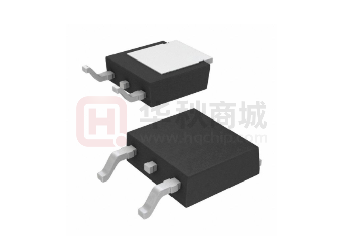


 工商网监
湘ICP备2023018690号
工商网监
湘ICP备2023018690号
