LP3350
Preliminary Datasheet
LED Driver with PWM Dimming Control
General Description
Features
LP3350 is a cost effective LED driver optimized for
LCD monitor and LCD TV backlighting application. It
provides a high performance LED backlight solution
with minimized bill of material count.
The LP3350 contains a PWM boost driver which
uses current mode control and fixed frequency
operation to regulate the LED current. The LED
current is sensed through an external current sense
resistor. The voltage across the sensing resistor is
compared with reference level of 0.3V, the error
amplified to control the pulse width of the power
switch thus to regulate the current flowing the LED.
Otherwise, The LP3350 offers external frequency
PWM dimming method for a wide range of dimming
control.
Other features include over current protection (OCP),
output over voltage protection (OVP), and
under-voltage lockout (UVLO). The
LP3350 is
available in a space saving SOP-8 (0.5mm pitch)
package.
Order Information
LP3350 □□□
Wide VIN Range: 8V to 28V
Current-Mode PWM Controller
External PWM Dimming Mode
Under-Voltage Lockout
Over Voltage Protection
Over Current Protection
Under-Voltage Protection
Over-Temperature Protection
Available in SOP-8
RoHS Compliant and Halogen Free
Pb-Free Package
Applications
TFT LCD TV
TFT LCD Monitor
Flat Panel Display
Marking Information
Device
Marking
Package
Shipping
LP3350
LPS
SOP-8
3K/REEL
LP3350
F: Green
Package Type
SO: SOP-8
LP3350–00 Version 0.3 NOV-2017
YWX
Y: Y is year code. W: W is week code. X: X is series number.
Email: marketing@lowpowersemi.com
www.lowpowersemi.com
Page 1 of 7
�LP3350
Preliminary Datasheet
Typical Application Circuit
L1
68uH
VIN
C1
220uF
R1
10Ω
C2
10uF
EN /
PWM
VIN
GATE
CS
GND
CTRL
OVP
FB
COMP
LP3350
ILED
LED
Lighting
R2
240kΩ
R5
0Ω
V+
C3
47uF
R6
1kΩ
R3
R7
0.18Ω 10kΩ
R8
100Ω
Rcomp
47kΩ
VRFB
1.5Ω
Ccomp
33nF
Figure 1. Typical Application Circuit of LP3350
Pin Configuration
VIN
1
8
CTRL
GATE
2
7
OVP
GND
3
6
COMP
CS
4
5
FB
Figure 2. SOP-8 Package Top View
LP3350–00 Version 0.3 NOV-2017
Email: marketing@lowpowersemi.com
www.lowpowersemi.com
Page 2 of 7
�LP3350
Preliminary Datasheet
Function Block Diagram
FB
COMP
EA and
Comp.
Internal
Regulator
VIN
UVLO
Control
Logic
EN / PWM
OVP OCP
OSC OTP
CTRL
OVP
CS
GATE
Gate
Driver
GND
Figure 3. Function Block Diagram
Functional Pin Description
Pin NO.
Pin Name
Description
1
VIN
2
GATE
External NMOS Gate Drive Pin.
3
GND
Ground.
4
CS
Current Sense Input Pin.
5
FB
Regulator Feedback Input. Connect to an external resistive to set the output current.
6
COMP
Input Supply Pin. Decouple with 10μF ceramic capacitor close to the pin.
Regulator Error Amplifier Compensation Pin.
7
OVP
Over Voltage Protection Sense Input. Connect to an external resistive voltage divider
from the V+ to GND.
8
CTRL
Enable and External PWM Dimming Control.
LP3350–00 Version 0.3 NOV-2017
Email: marketing@lowpowersemi.com
www.lowpowersemi.com
Page 3 of 7
�LP3350
Preliminary Datasheet
Absolute Maximum Ratings Note 1
VIN to GND -------------------------------------------------------------------------------------------------------- −0.3V to +36V
GATE, CS, FB, COMP, OVP, CTRL to GND ------------------------------------------------------------- −0.3V to +20V
Operating Junction Temperature Range (TJ)
Operation Ambient Temperature Range -------------------------------------------------------------- −40°C to +85°C
Storage Temperature Range ---------------------------------------------------------------------------- −65°C to +150°C
Maximum Soldering Temperature (at leads, 10sec) ----------------------------------------------- +260°C
Maximum Junction Temperature ----------------------------------------------------------------------- +150°C
------------------------------------------------------ −40℃ to +150℃
Note 1. Stresses beyond those listed under “Absolute Maximum Ratings” may cause permanent damage to the device. These are stress
ratings only, and functional operation of the device at these or any other conditions beyond those indicated in the operational sections of
the specifications is not implied. Exposure to absolute maximum rating conditions for extended periods may affect device reliability.
Thermal Information
Thermal Resistance
SOP-8, θJA ---------------------------------------------------------------------------------------------------- 112°C/W
SOP-8, θJC ---------------------------------------------------------------------------------------------------- 39°C/W
LP3350–00 Version 0.3 NOV-2017
Email: marketing@lowpowersemi.com
www.lowpowersemi.com
Page 4 of 7
�LP3350
Preliminary Datasheet
Electrical Characteristics
(VIN=12V, VCTRL=5V, TA=25°C, unless otherwise specified)
Parameter
Symbol
Test Conditions
Min
Typ
Max
Units
28
V
General
Input Supply Voltage
VIN Supply Current
VVLI
8
Sleep Current
310
400
uA
Operation Current
2.5
3
mA
7
8
V
IQ
Input UVLO Threshold
VUVLO(VTH)
V IN Rising
UVLO Threshold Hysteresis
VUVLO(HYS)
Falling Hysteresis
Soft Start Slope
6
TSS_Slop
Thermal Shutdown Threshold
TSD
Thermal Shutdown Hysteresis
∆TSD
Temperature Rising
140
500
mV
400
mV/ms
160
180
30
°C
°C
PWM Control
Internal Oscillator Frequency
FOSC
175
200
225
kHz
Maximum Duty Cycle
DMAX
93
95
97
%
VIH
Logic High.
VIL
Logic Low
2.6
V
CTRL Threshold Voltage
Pull Down Resistor
1
RPull_Low
150
kΩ
Error Amplifier
Reference
voltage
non-inverting input.
at
Reference Voltage
VREF
Open Loop Voltage Gain
Am
Transconductance of EA
Gm
80
100
120
uA/V
ISource
24
30
36
uA
ISink
48
60
72
uA
1.8
2
2.2
V
GATE Source Current
GATE Sink Current
295.5
300
304.5
70
mV
dB
Protection Threshold
Over Voltage Protection
VOVP
Threshold of OVP
Over Current Protection
VOCP
Threshold of OCP
Fault Trigger Duration
Connect detect time
SCP Threshold
LP3350–00 Version 0.3 NOV-2017
330
mV
TFault
50
ms
TDly
1
ms
Normal Operation
200
mV
System Startup
100
mV
VOVP_UV
Email: marketing@lowpowersemi.com
www.lowpowersemi.com
Page 5 of 7
�LP3350
Preliminary Datasheet
Application Information
LP3350–00 Version 0.3 NOV-2017
1. Connected all ground together with one
uninterrupted ground plane with at least two vias .
2. The input capacitor should be located as closed
as possible to the VIN and ground plane.
3. Minimize the distance of all traces connected to
the LX node, that the traces short and wide route
to obtain optimum efficiency.
4. All output capacitor must be closed to ground
plane.
The ground terminal of COUT must be located as
closed as possible to ground plane.
5. Radiated noise can be decreased by choosing
a shielded inductor.
VIN
V+
Rin
GND
G
1
8
2
7
3
6
4
LP3350
5
S
R6
R7
R3
COUT
Diode
L
CIN
Boost Loop Compensation
The feedback loop can be compensated with an
external compensation network consisted of Rcomp,
Ccomp (As Figure 1). Choosing Rcomp to set high
frequency integrator gain for fast transient response
and Ccomp to set the integrator zero to maintain loop
stability.
Over Voltage Protection
The LP3350 converter has an over voltage protection
by OVP pin. When the LEDs fail open circuit or LEDs
are disconnected from the circuit, the over voltage
function will monitor the output voltage through OVP
pin to protect the converter. When LP3350 occur
OVP, it will latch off until VIN is re-startup or CTRL
input is recycled.
LED Current Setting
The LED current is specified by current sense resistor
between the FB pin to ground. In order to have
accurate LED current, precision resistors are
preferred. The LED current can be programmed by:
ILED=0.3/RFB
Dimming Control
The LED brightness is controlled by the PWM signal
at CTRL pin which has different duty cycle. LP3350
can accept an external PWM signal to CTRL pin in the
range of 100Hz to 1 kHz.
Over Temperature Protection
The LP3350 device enters over temperature
protection(OTP) if its junction temperature exceeds
160°C (Typ.). During over temperature protection
none of the device's functions are available. To
resume normal operation the junction temperature
need cool down, and the outputs will restart.
Layout Guideline
The proper PCB layout and component placement
are critical for all circuit. The careful attention
should be prevent electromagnetic interference
(EMI) problems. Here are some suggestions to the
layout of LP3350 design.
Cin
The LP3350 is designed in a current mode, constant
frequency PWM boost converter. It can use dimming
input that can by external control signal with a duty
ratio of 1%-100% in 100Hz to 1kHz. LP3350 offers
protection features to protect the system such as
output over voltage protection, boost diode
disconnection protection, output short circuit
protection and over temperature protection.
Under Voltage Lockout (UVLO)
The LP3350 had an UVLO internal circuit that enable
the device once the voltage on the VIN voltage
exceeds the UVLO threshold voltage.
Boost Controller
The LP3350 uses 200kHz fixed-frequency, current
mode architecture to fixed the output current. The
output voltage and soft start time can be adjustable by
internal register.
GND
R2
RComp
CComp
R8
RFB
V-
Figure 4. Recommended PCB Layout Diagram
.
Email: marketing@lowpowersemi.com
www.lowpowersemi.com
Page 6 of 7
�LP3350
Preliminary Datasheet
Outline Information
SOP-8 Package (Unit: mm)
D
LPS
LP3350
YWX
E
E1
1
b
DIMENSION IN MILLIMETER
SYMBOLS
UNIT
MIN
NOM
MAX
A
--
--
1.750
A1
0.100
--
0.225
A2
1.300
1.400
1.500
A3
0.600
0.650
0.700
b
0.390
--
0.470
D
4.800
4.900
5.000
E
5.800
6.000
6.200
E1
3.800
3.900
4.000
e
e
L
1.27BSC
0.500
--
0.800
A3
A1
A
A2
L
LP3350–00 Version 0.3 NOV-2017
Email: marketing@lowpowersemi.com
www.lowpowersemi.com
Page 7 of 7
�
很抱歉,暂时无法提供与“LP3350SOF”相匹配的价格&库存,您可以联系我们找货
免费人工找货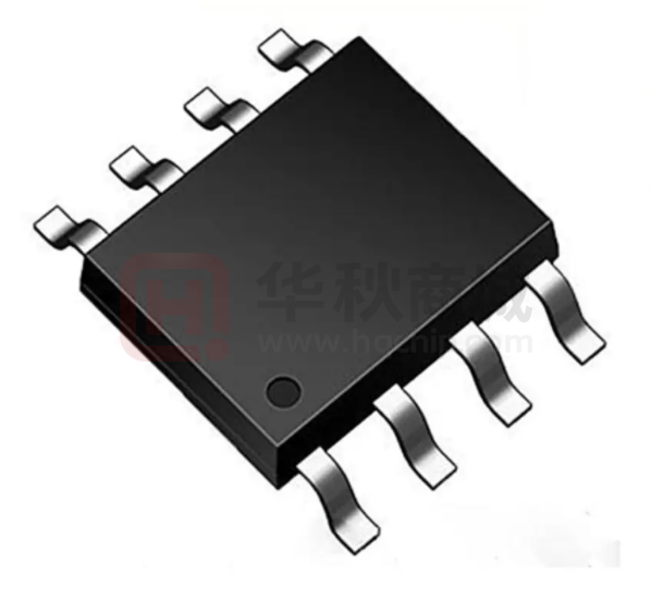


 工商网监
湘ICP备2023018690号
工商网监
湘ICP备2023018690号
