LM317
HIGH CURRENT ADJUSTABLE VOLTAGE REGULATOR
General Description
The LM317 is an adjustable 3−terminal positive voltage regulator capable of
supplying in excess of 1.5 A over an output voltage range of 1.2 V to 37 V. This
voltage regulator is exceptionally easy to use and requires only two external
resistors to set the output voltage. Further, it employs internal current limiting,
thermal shutdown and safe area compensation, making it essentially blow−out
proof.
The LM317 serves a wide variety of applications including local, on card
regulation. This device can also be used to make a programmable output regulator,
or by connecting a fixed resistor between the adjustment and output, the LM317
can be used as a precision current regulator.
Features
Output Current in Excess of 1.5 A
Output Adjustable between 1.2 V and 37 V
Internal Thermal Overload Protection
Internal Short Circuit Current Limiting Constant with Temperature
Output Transistor Safe−Area Compensation
Floating Operation for High Voltage Applications
Eliminates Stocking many Fixed Voltages
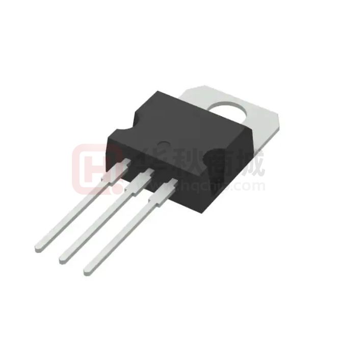
Available in Surface Mount D2PAK−3, and Standard 3−Lead Transistor Package
NCV Prefix for Automotive and Other Applications Requiring Unique Site and Control Change
Requirements; AEC−Q100 Qualified and PPAP Capable
These Devices are Pb−Free, Halogen Free/BFR Free and are RoHS Compliant
Ordering Information
DEVICE
Package Type
MARKING
Packing
Packing QTY
LM317S
SOT-223
LM317S
Tape
3000/Reel
LM317T
T0-220
LM317T
Tube
1000/BOX
LM317MDTR
TO-252-2L
LM317M
Tape
2500/Reel
LM317CDTR
TO-263-3L
LM317C
Tape
1000/Reel
XBLWversion1.0
文档仅供参考,实际应用测试为准
www.xinboleic.com
技术支持热线:4009682003
第 1 页 共 13 页
�LM317
HIGH CURRENT ADJUSTABLE VOLTAGE REGULATOR
Block Diagram
2.1 Block Diagram
Figure 1. Standard Application
Absolute Maximum Rratings
Rating
Input-Output Voltage Differential
Power Dissipation
Case 221A
TA=+25℃
Thermal Resistance, Junction-to-Ambient
Thermal Resistance, Junction-to-Case
Case 936 (D²PAK-3)
TA=+25℃
Thermal Resistance, Junction-to-Ambient
Thermal Resistance,Junction-to-Case
Operating Junction Temperature Range
Storage Temperature Range
XBLWversion1.0
Symbol
VI-VO
Value
-0.3 to 40
Unit
Vdc
PD
θJA
θJC
Internally Limited
65
5.0
W
℃/W
℃/W
PD
θJA
θJC
TJ
Tstg
Internally Limited
70
5.0
-55 to+150
-65 to+150
W
℃/W
℃/W
℃
℃
文档仅供参考,实际应用测试为准
www.xinboleic.com
技术支持热线:4009682003
第 2 页 共 13 页
�LM317
HIGH CURRENT ADJUSTABLE VOLTAGE REGULATOR
Stresses exceeding those listed in the Maximum Ratings table may damage the device. If any of
these limits are exceeded, device functionality
should not be assumed, damage may occur and reliability may be affected.
Electrical Characteristics
(VI-VO=5V, IO=0.5A for D2T and T packages;TJ=Tlow to Thigh(Note1);Imax and
Pmax(Note2);unless otherwise noted.)
Characteristics
Line Regulation (Note3), TA=+25℃,3.0V≤VI-VO≤40V
Load Regulation (Note3),TA=+25℃,10mA≤IO≤lmax
Vo≤5.0V
Vo≥5.0V
Thermal Regulation, TA=+25℃ (Note 4), 20 ms Pulse
Adjustment Pin Current
Adjustment Pin Current Change,2.5V≤VI-VO≤40V,
10mA≤ IL≤Imax,PD≤Pmax
Reference Voltage,3.0V≤VI-VO≤40V,10mA≤IO≤Imax,PD≤Pmax
Line Regulation (Note3), 3.0V≤VI-VO≤40V
Load Regulation (Note3),10 mA≤IO≤Imax
VO≤5.0V
VO≥5.0V
Temperature Stability (Tlow≤TJ≤Thigh)
Minimum Load Current to Maintain Regulation (VI-VO = 40V)
Maximum Output Current
VI-VO≤15V,PD≤Pmax.T Package
VI-VO=40V,PD≤Pmax,TA=+25℃,T Package
RMS Noise,% of VO,TA=+25℃,10Hz≤f≤10kHz
Ripple Rejection, VO = 10V,f=120Hz (Note5)
Without CAdj
CAdj =10μF
Thermal Shutdown (Note6)
Long-Term Stability, TJ = Thigh (Note7), TA =+25℃ for
Endpoint Measurements
Thermal Resistance Junction-to-Case, T Package
Figure
1
Symbol
Regline
2
Regload
Min
-
Typ
0.01
Max
0.04
Unit
%/V
-
5.0
0.1
25
0.5
mV
% Vo
-
Regtherm
-
0.03
0.07
% Vo/W
3
1,2
IAdj
∆IAdj
-
50
0.2
100
5.0
μA
μA
3
1
2
Vref
Regline
Regload
1.2
-
1.25
0.02
1.3
0.07
V
%/V
3
3
3
TS
-
20
0.3
0.7
3.5
70
1.5
10
1.5
0.15
2.2
0.4
-
mV
% Vo
% Vo
mA
A
-
0.003
-
65
80
180
0.3
1.0
5.0
-
ILmin
Imax
-
N
4
RR
3
S
66
-
-
RθJC
-
% Vo
dB
℃
%/1.0
kHrs.
℃/W
1. Tlow to Thigh = 0° to +125℃, for LM317, D2T. Tlow to Thigh = −40° to +125℃, for
LM317BT, BD2T, Tlow to Thigh = −55° to +150℃, for LM317BT, BD2T.
2. Imax = 1.5A, Pmax = 20W
3. Load and line regulation are specified at constant junction temperature. Changes in VO due
to heating effects must be taken into account separately. Pulse testing with low duty cycle is
used.
4. Power dissipation within an IC voltage regulator produces a temperature gradient on the die,
affecting individual IC components on the die.
These effects can be minimized by proper integrated circuit design and layout techniques.
Thermal Regulation is the effect of these
temperature gradients on the output voltage and is expressed in percentage of output change per
watt of power change in a specified time.
5. CAdj, when used, is connected between the adjustment pin and ground.
6. Thermal characteristics are not subject to production test.
7. Since Long−Term Stability cannot be measured on each device before shipment, this
specification is an engineering estimate of average stability from lot to lot.
XBLWversion1.0
文档仅供参考,实际应用测试为准
www.xinboleic.com
技术支持热线:4009682003
第 3 页 共 13 页
�LM317
HIGH CURRENT ADJUSTABLE VOLTAGE REGULATOR
Application Circuit
Figure 2. Representative Schematic Diagram
Figure 3. Line Regulation and ∆IAdj/Line Test Circuit
XBLWversion1.0
文档仅供参考,实际应用测试为准
www.xinboleic.com
技术支持热线:4009682003
第 4 页 共 13 页
�LM317
HIGH CURRENT ADJUSTABLE VOLTAGE REGULATOR
Figure 4. Load Regulation and ∆IAdj/Load Test Circuit
Figure 5. Standard Test Circuit
XBLWversion1.0
文档仅供参考,实际应用测试为准
www.xinboleic.com
技术支持热线:4009682003
第 5 页 共 13 页
�LM317
HIGH CURRENT ADJUSTABLE VOLTAGE REGULATOR
Figure 6. Ripple Rejection Test Circuit
Characteristics Curves
Figure 7. Load Regulation Figure
Figure 9. Adjustment Pin Current Figure
Figure 11. Temperature Stability Figure
XBLWversion1.0
8. Current Limit
10. Dropout Voltage
12. Minimum Operating Current
文档仅供参考,实际应用测试为准
www.xinboleic.com
技术支持热线:4009682003
第 6 页 共 13 页
�LM317
HIGH CURRENT ADJUSTABLE VOLTAGE REGULATOR
Figure 13. Ripple Rejection versus Output
Voltage
Figure 15. Ripple Rejection versus Frequency
Figure 17. Line Transient Response
XBLWversion1.0
Figure 14. Ripple Rejection versus
Output Current
Figure 16. Output Impedance
Figure 18. Load Transient Response
文档仅供参考,实际应用测试为准
www.xinboleic.com
技术支持热线:4009682003
第 7 页 共 13 页
�LM317
Voltage Regulator-Adjustable Output,Positive 1.5A
Basic Circuit Operation
The LM317 is a 3−terminal floating regulator. In operation, the LM317 develops and maintains a nominal 1.25 V
reference (Vref) between its output and adjustment
terminals. This reference voltage is converted to a programming current (IPROG) by R1 (see Figure 17), and this constant
current flows through R2 to ground.
The regulated output voltage is given by:
�
VOUT=Vref � + �� +IAdjR2
�
Since the current from the adjustment terminal (IAdj) represents an error term in the equation, the LM317 was
designed to control IAdj to less than 100μA and keep it
constant. To do this, all quiescent operating current is returned to the output terminal. This imposes the requirement for
a minimum load current. If the load current is less than this minimum, the output voltage will rise. Since the LM317 is
a floating regulator, it is only the voltage differential across the circuit which is important to performance, and
operation at high voltages with respect to ground is possible.
Load Regulation
Figure 19. Basic Circuit Configuration
The LM317 is capable of providing extremely good load regulation, but a few precautions are needed to obtain
maximum performance. For best performance, the programming resistor (R1) should be connected as close to the
regulator as possible to minimize line drops which effectively appear in series with the reference, thereby degrading
regulation. The ground end of R2 can be returned near the load ground to provide remote ground sensing and improve
load regulation.
External Capacitors
A 0.1μF disc or 1.0μF tantalum input bypass capacitor (Cin) is recommended to reduce the sensitivity to input line impedance.
The adjustment terminal may be bypassed to ground to improve ripple rejection. This capacitor (CAdj) prevents ripple from being
amplified as the output voltage is increased. A 10μF capacitor should improve ripple rejection about 15dB at 120Hz in a 10V application.
Although the LM317 is stable with no output capacitance, like any feedback circuit, certain values of external capacitance can cause
excessive ringing. An output
capacitance (CO) in the form of a 1.0μF tantalum or 25μF aluminum electrolytic capacitor on the output swamps this effect and insures
stability.
Protection Diodes
When external capacitors are used with any IC regulator it is sometimes necessary to add protection diodes to
prevent the capacitors from discharging through low current points into the regulator.
Figure 18 shows the LM317 with the recommended protection diodes for output voltages in excess of 25μV or
high capacitance values (CO > 25μF, CAdj > 10μF). Diode D1 prevents CO from discharging thru the IC during an input
short circuit. Diode D2 protects against capacitor CAdj discharging through the IC during an output short circuit. The
combination of diodes D1 and D2 prevents CAdj from discharging through the IC during an input short circuit.
XBLWversion1.0
文档仅供参考,实际应用测试为准
www.xinboleic.com
技术支持热线:4009682003
第 8 页 共 13 页
�LM317
Voltage Regulator-Adjustable Output,Positive 1.5A
Figure 20. Voltage Regulator with Protection Diodes
Figure 21. D2PAK Thermal Resistance and Maximum
Power Dissipation versus P.C.B. Copper Length
Figure 22. ‘‘Laboratory’’ Power Supply with Adjustable
XBLWversion1.0
文档仅供参考,实际应用测试为准
www.xinboleic.com
技术支持热线:4009682003
第 9 页 共 13 页
�LM317
Voltage Regulator-Adjustable Output,Positive 1.5A
Figure 23. Adjustable Current Limiter Figure
Figure 25. Slow Turn−On Regulator Figure
24. 5.0 V Electronic Shutdown Regulator
26. Current Regulator
Outline Drawing
SOT223
XBLWversion1.0
Unit:mm
文档仅供参考,实际应用测试为准
www.xinboleic.com
技术支持热线:4009682003
第 10 页 共 13 页
�LM317
Voltage Regulator-Adjustable Output,Positive 1.5A
XBLWversion1.0
TO220
Unit:mm
TO252
Unit:mm
文档仅供参考,实际应用测试为准
www.xinboleic.com
技术支持热线:4009682003
第 11 页 共 13 页
�LM317
Voltage Regulator-Adjustable Output,Positive 1.5A
TO263
Unit:mm
Current Limit and Output Voltage
XBLWversion1.0
文档仅供参考,实际应用测试为准
www.xinboleic.com
技术支持热线:4009682003
第 12 页 共 13 页
�LM317
Voltage Regulator-Adjustable Output,Positive 1.5A
Statement:
Shenzhen xinbole electronics co., ltd. reserves the right to change the product specifications, without notice!
Before placing an order, the customer needs to confirm whether the information obtained is the latest version,
and verify the integrity of the relevant information.
Any semiconductor product is liable to fail or malfunction under certain conditions, and the buyer shall be
responsible for complying with safety standards in the system design and whole machine manufacturing using
Shenzhen xinbole electronics co., ltd products, and take appropriate security measures to avoid the potential risk
of failure may result in personal injury or property losses of the situation occurred!
Product performance is never ending, Shenzhen xinbole electronics co., ltd will be dedicated to provide
customers with better performance, better quality of integrated circuit products.
XBLWversion1.0
文档仅供参考,实际应用测试为准
www.xinboleic.com
技术支持热线:4009682003
第 13 页 共 13 页
�


 工商网监
湘ICP备2023018690号
工商网监
湘ICP备2023018690号
