XBLW LMV321A, LMV358A, LMV324A
1MHz, General Purpose, RRIO CMOS Amplifiers
General Description
The XBLW LMV321A (single), XBLW LMV358A (dual) and XBLW LMV324A (quad) are general purpose,
low offset, high frequency response and micro power operational amplifiers. With an excellent bandwidth of 1MHz, a
slew rate of 0.8V/μs, and a quiescent current of 80μA per amplifier at 5V, the XBLW LMV321A/358A/324A family
can be designed into a wide range of applications.
The XBLW LMV321A/358A/324A op-amps are designed to provide optimal performance in low voltage and low
power systems. The input common-mode voltage range includes ground, and the maximum input offset voltage are
4.5mV. These parts provide rail-to-rail output swing into heavy loads. The XBLW LMV321A/358A/324A family is
specified for single or dual power supplies of +2.3V to +5.5V. All models are specified over the extended industrial
temperature range of -40℃ to +125℃.
The XBLW LMV321A is available in 5-lead SOT-23 and SC70-5 package. The XBLW LMV358A is available in
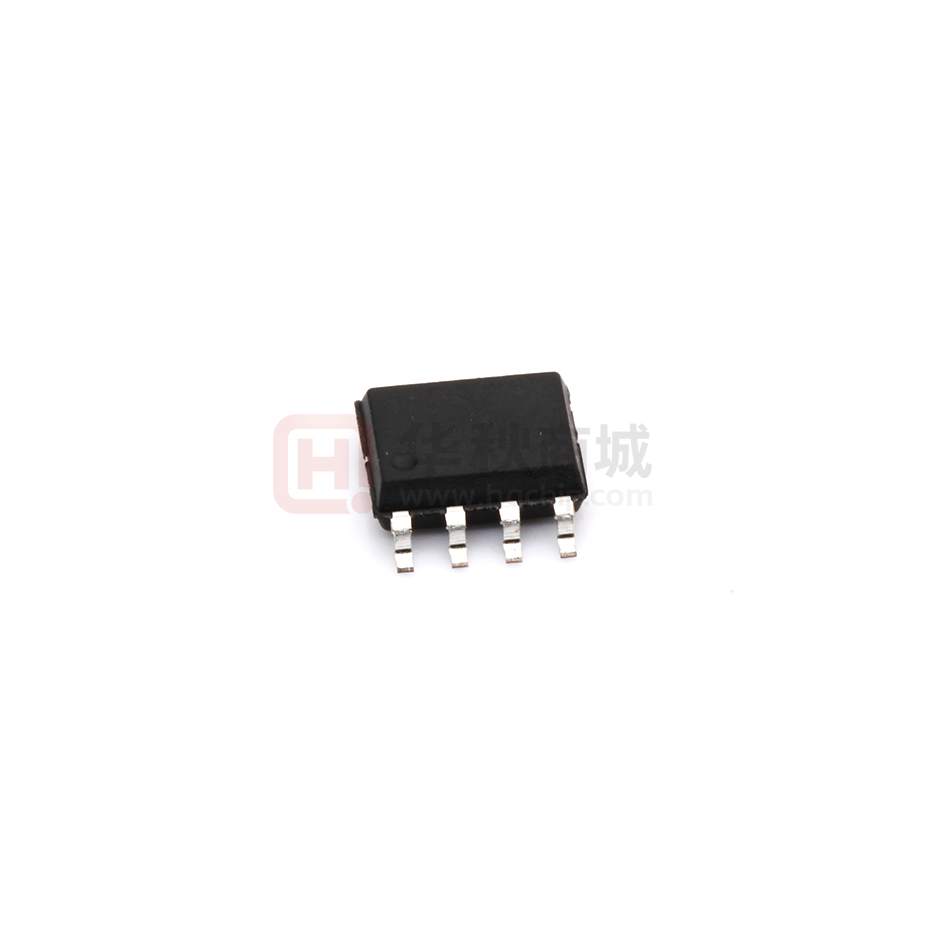
8-lead SOP package. The XBLW LMV324A is available in 14-lead SOP package.
Features
General Purpose 1MHz Amplifiers, Low Cost
High Slew Rate: 0.8V/μs
Low Offset Voltage: 4.5 mV Maximum
Low Power: 80μA per Amplifier Supply Current
Settling Time to 0.1% with 2V Step: 4.2 μs
Unit Gain Stable
Rail-to-Rail Input and Output
Input Voltage Range: -0.1V to +5.1V at 5V Supply
Operating Power Supply: +2.3V to +5.5V
Operating Temperature Range: -40℃ to +125℃
ESD Rating: HBM-4kV, CDM-2kV
Upgrade to LMV321A/LMV358A/LMV324A Family
Applications
Smoke/Gas/Environment Sensors
Audio Outputs
Battery and Power Supply Control
Portable Equipment and Mobile Devices
Active Filters
Sensor Interfaces
Battery-Powered Instrumentation
Medical Instrumentation
Ordering Information
DEVICE
Package Type
MARKING
Packing
Packing QTY
LMV321ATDTR
SOT23-5
V321A
Tape
3000/Reel
LMV321ACDTR
SC70-5
V321A
Tape
3000/Reel
LMV358ADTR
SOP-8
LMV358A
Tape
2500/Reel
LMV358AMDTR
MSOP-8
V358AM
Tape
3000/Reel
LMV358ATDTR
TSSOP-8
V358AT
Tape
3000/Reel
LMV324ADTR
SOP-14
LMV324A
Tape
2500/Reel
LMV324ATDTR
TSSOP-14
V324AT
Tape
2500/Reel
XBLWversion1.0
文档仅供参考,实际应用测试为准
www.xinboleic.com
技术支持热线:4009682003
第 1 页 共 12 页
�XBLW LMV321A, LMV358A, LMV324A
1MHz, General Purpose, RRIO CMOS Amplifiers
Pin Configurations
LMV321A
LMV358A
LMV324A
Figure 1 Pin Configurations
Pin Description
Symbol
Description
-IN
Negative (inverting) input.
+IN
Positive (noninverting) input.
-INA, -INB
-INC, -IND
Inverting Input of the Amplifier. The Voltage range can go from (VS– – 0.1V) to (VS+ + 0.1V).
+INA, +INB
+INC, +IND
Non-Inverting Input of Amplifier. This pin has the same voltage range as -IN.
Positive Power Supply. The voltage is from 2.3V to 5.5V. Split supplies are possible as long as
the voltage between VS+ and VS– is between 2.3V and 5.5V. A bypass capacitor of 0.1μF as
close to the part as possible should be used between power supply pins or between supply pins
and ground
+VS
Negative Power Supply. It is normally tied to ground. It can also be tied to a voltage other
than ground as long as the voltage between VS+ and VS– is from 2.3V to 5.5V. If it is not
connected to ground, bypass it with a capacitor of 0.1μF as close to the part as possible.
-VS
OUT
Output.
OUTA, OUTB
OUTC, OUTD
Amplifier Output
Absolute Maximum Ratings (TA= 25℃)
Symbol
Description
Value
Units
VS+,V S-
Supply Voltage, VS+ to VS–
7.0
V
VCM
Common-Mode Input Voltage
VS– – 0.3 to VS+ + 0.3
V
HBM ±4000
V
ESD
Electrostatic Discharge Voltage
CDM ±2000
V
TJ
Junction Temperature
160
°C
TSTG
Storage Temperature Range
-65 to +150
°C(TJ)
TJL
Lead Temperature Range
(Soldering 10 sec)
260
°C
Notes:
1. Stresses beyond those listed under Absolute Maximum Ratings may cause permanent damage to the device. These are stress ratings
only, which do not imply functional operation of the device at these or any other conditions beyond those indicated under
XBLWversion1.0
文档仅供参考,实际应用测试为准
www.xinboleic.com
技术支持热线:4009682003
第 2 页 共 12 页
�XBLW LMV321A, LMV358A, LMV324A
1MHz, General Purpose, RRIO CMOS Amplifiers
Recommended Operating Conditions. Exposure to absolute-maximum-rated conditions for extended periods may affect device
reliability.
2. Provided device does not exceed maximum junction temperature (TJ) at any time.
Electrical Characteristics
VS = 5.0V, TA = +25℃, VCM = VS/2, VO = VS/2, and RL = 10kΩ connected to VS/2, unless otherwise noted.
Symbol
Parameter
Conditions
Min.
Typ.
Max.
Input offset voltage
-4.5
±1.0
+4.5
Over temperature
-4.8
Unit
INPUT CHARACTERISTICS
VOS
VOS TC
1
Over temperature
500
Input offset current
1
VCM
Common-mode voltage
range
Common-mode rejection
ratio
Over temperature
CMRR
AVOL
Over temperature
Input resistance
CIN
Input capacitance
pA
pA
VS++0.1
V
90
VCM = 0.05V to 3.5V
80
VCM = VS––0.1 to VS++0.1 V
Open-loop voltage gain
RIN
VS––0.1
85
Over temperature
μV/°C
2.3
Input bias current
IB
IOS
Over Temperature
Offset voltage drift
mV
+4.8
dB
75
110
VO = 0.05 to 3.5 V
100
dB
GΩ
100
Differential
2.0
Common mode
3.5
pF
OUTPUT CHARACTERISTICS
VOH
High output voltage swing
VS+ –8
mV
VOL
Low output voltage swing
8
mV
ZOUT
ISC
Closed-loop output
impedance
Open-loop output
impedance
Short-circuit current
f = 200kHz, G = +1
0.4
f = 1MHz, IO = 0
2.6
Source current through 10Ω
40
Sink current through 10Ω
40
f = 1kHz
1.0
MHz
CL = 100pF
62
°
G = +1, CL = 100pF, VO
= 1.5V to 3.5V
0.8
V/μs
Ω
mA
DYNAMIC PERFORMANCE
GBW
Gain bandwidth product
ΦM
SR
XBLWversion1.0
Phase margin
Slew rate
文档仅供参考,实际应用测试为准
www.xinboleic.com
技术支持热线:4009682003
第 3 页 共 12 页
�XBLW LMV321A, LMV358A, LMV324A
1MHz, General Purpose, RRIO CMOS Amplifiers
Electrical Characteristics
VS = 5.0V, TA = +25℃, VCM = VS/2, VO = VS/2, and RL = 10kΩ connected to VS/2, unless otherwise noted.
Symbol
Parameter
tS
Settling time
Conditions
Min.
To 0.1%, G = +1, 2V step
Overload recovery time
THD+N
Total harmonic
distortion+Noise
Max.
4.2
To 0.01%, G = +1, 2V step
tOR
Typ.
Unit
μs
5.2
VIN * Gain > VS
f = 1kHz, G = +1, VO=3VPP
2
μs
0.003
%
13
μVP-P
NOISE PERFORMANCE
Vn
Input voltage noise
f = 0.1 to 10 Hz
en
Input voltage noise density
f = 1kHz
35
nV/√Hz
In
Input current noise density
f = 10kHz
6
fA/√Hz
POWER SUPPLY
VS
PSRR
Operating supply voltage
Power supply rejection ratio
Over temperature
IQ
2.3
5.5
98
VS = 2.7V to 5.5V, VCM
< VS+ − 2V
V
dB
85
Quiescent current
(per amplifier)
80
120
Over temperature
85
130
μA
THERMAL CHARACTERISTICS
TA
θJA
Operating temperature range
-40
Package thermal resistance
+125
SOT23-5
190
SO-8
125
SO-14
115
°C
℃/W
Specifications subject to changes without notice
XBLWversion1.0
文档仅供参考,实际应用测试为准
www.xinboleic.com
技术支持热线:4009682003
第 4 页 共 12 页
�XBLW LMV321A, LMV358A, LMV324A
1MHz, General Purpose, RRIO CMOS Amplifiers
Typical Performance Characteristics
At TA = +25℃, VCM = VS/2, and RL = 10kΩ connected to VS/2, unless otherwise noted.
Figure 2 Open-loop Gain and Phase as
function of Frequency
Figure 3 Power Supply and Common-mode RejectionRatio a
as a function of Frequency
Figure 4 Input Offset Voltage Production DistributionFigure 5 Channel Separation as a function of Frequency
Figure 6 Large-Signal Step Response at 2.7V
Figure 8 Large-Signal Step Response at 5V
XBLWversion1.0
Figure 7 Small-Signal Step Response at 2.7V
Figure 9 Small-Signal Step Response at 5V
文档仅供参考,实际应用测试为准
www.xinboleic.com
技术支持热线:4009682003
第 5 页 共 12 页
�XBLW LMV321A, LMV358A, LMV324A
1MHz, General Purpose, RRIO CMOS Amplifiers
Application Notes
1. LOW INPUT BIAS CURRENT
The XBLW LMV321A/358A/324A family is a CMOS op-amp family and features very low input bias current in
pA range. The low input bias current allows the amplifiers to be used in applications with high resistance sources. Care
must be taken to minimize PCB Surface Leakage. See below section on “PCB Surface Leakage” for more details.
2. PCB SURFACE LEAKAGE
In applications where low input bias current is critical, Printed Circuit Board (PCB) surface leakage effects need to
be considered. Surface leakage is caused by humidity, dust or other contamination on the board. Under low humidity
conditions, a typical resistance between nearby traces is 1012Ω. A 5V difference would cause 5pA of current to flow,
which is greater than the XBLW LMV321A/358A/324A’s input bias current at +25℃ (±1fA, typical). It is recommended
to use multi-layer PCB layout and route the op-amp’s -IN and +IN signal under the PCB surface.
The effective way to reduce surface leakage is to use a guard ring around sensitive pins (or traces). The guard ring
is biased at the same voltage as the sensitive pin. An example of this type of layout is shown in Figure 10 for Inverting
Gain application.
1. For Non-Inverting Gain and Unity-Gain Buffer:
a) Connect the non-inverting pin (+IN) to the input with a wire that does not touch the PCB surface.
b) Connect the guard ring to the inverting input pin (-IN). This biases the guard ring to the Common Mode input
voltage.
2. For Inverting Gain and Trans-impedance Gain Amplifiers (convert current to voltage, such as photo detectors):
a) Connect the guard ring to the non-inverting input pin (+IN). This biases the guard ring to the same reference
voltage as the op-amp (e.g., VS/2 or ground).
b) Connect the inverting pin (-IN) to the input with a wire that does not touch the PCB surface.
3. GROUND SENSING AND RAIL TO RAIL
The input common-mode voltage range of the XBLW LMV321A/358A/324A series extends 100mV beyond the
supply rails. This is achieved with a complementary input stage—an N- channel input differential pair in parallel with a P
-channel differential pair. For normal operation, inputs should be limited to this range. The absolute maximum input
voltage is 300mV beyond the supplies. Inputs greater than the input common-mode range but less than the maximum
input voltage, while not valid, will not cause any damage to the op-amp. Unlike some other op-amps, if input current is
limited, the inputs may go beyond the supplies without phase inversion, as shown in Figure 11. Since the input commonmode range extends from (VS− − 0.1V) to (VS+ + 0.1V), the XBLW LMV321A/358A/324A op-amps can easily perform
‘true ground’ sensing.
Figure 11 No Phase Inversion with Inputs Greater Than the Power-Supply Voltage
XBLWversion1.0
文档仅供参考,实际应用测试为准
www.xinboleic.com
技术支持热线:4009682003
第 6 页 共 12 页
�XBLW LMV321A, LMV358A, LMV324A
1MHz, General Purpose, RRIO CMOS Amplifiers
ail-to-rail output. For light resistive loads (e.g. 100kΩ), the output voltage can typically swing to within 5mV from
the supply rails. With moderate resistive loads (e.g. 10kΩ), the output can typically swing to within 10mV from the
supply rails and maintain high open-loop gain.
The maximum output current is a function of total supply voltage. As the supply voltage to the amplifier increases,
the output current capability also increases. Attention must be paid to keep the junction temperature of the IC below
150°C when the output is in continuous short-circuit. The output of the amplifier has reverse-biased ESD diodes
connected to each supply. The output should not be forced more than 0.5V beyond either supply, otherwise current will
flow through these diodes.
4. CAPACITIVE LOAD AND STABILITY
The XBLW LMV321A/358A/324A can directly drive 1nF in unity-gain without oscillation. The unity-gain
follower (buffer) is the most sensitive configuration to capacitive loading. Direct capacitive loading reduces the phase
margin of amplifiers and this results in ringing or even oscillation. Applications that require greater capacitive drive
capability should use an isolation resistor between the output and the capacitive load like the circuit in Figure 12. The
isolation resistor RISO and the load capacitor CL form a zero to increase stability. The bigger the RISO resistor value, the
more stable VOUT will be. Note that this method results in a loss of gain accuracy because RISO forms a voltage divider
with the RL.
Figure 12 Indirectly Driving Heavy Capacitive Load
An improvement circuit is shown in Figure 13. It provides DC accuracy as well as AC stability. The RF provides
the DC accuracy by connecting the inverting signal with the output. The CF and RISO serve to counteract the loss of phase
margin by feeding the high frequency component of the output signal back to the amplifier’s inverting input, thereby
preserving phase margin in the overall feedback loop.
Figure 13 Indirectly Driving Heavy Capacitive Load with DC Accuracy
For no-buffer configuration, there are two others ways to increase the phase margin: (a) by increasing the
amplifier’s gain, or (b) by placing a capacitor in parallel with the feedback resistor to counteract the parasitic capacitance
associated with inverting node.
5. POWER SUPPLY LAYOUT AND BYPASS
The XBLW LMV321A/358A/324A family operates from either a single +2.3V to +5.5V supply or dual ±1.15V to
±2.75V supplies. For single-supply operation, bypass the power supply VS with a ceramic capacitor (i.e. 0.01μF to 0.1μF)
which should be placed close (within 2mm for good high frequency performance) to the VS pin. For dual-supply
operation, both the VS+ and the VS- supplies should be bypassed to ground with separate 0.1μF ceramic capacitors. A bulk
capacitor (i.e. 2.2μF or larger tantalum capacitor) within 100mm to provide large, slow currents and better performance.
This bulk capacitor can be shared with other analog parts.
XBLWversion1.0
文档仅供参考,实际应用测试为准
www.xinboleic.com
技术支持热线:4009682003
第 7 页 共 12 页
�XBLW LMV321A, LMV358A, LMV324A
1MHz, General Purpose, RRIO CMOS Amplifiers
Good PC board layout techniques optimize performance by decreasing the amount of stray capacitance at the opamp’s inputs and output. To decrease stray capacitance, minimize trace lengths and widths by placing external
components as close to the device as possible. Use surface-mount components whenever possible. For the op-amp,
soldering the part to the board directly is strongly recommended. Try to keep the high frequency big current loop area
small to minimize the EMI (electromagnetic interfacing).
6. GROUNDING
A ground plane layer is important for the XBLW LMV321A/358A/324A circuit design. The length of the current
path speed currents in an inductive ground return will create an unwanted voltage noise. Broad ground plane areas will
reduce the parasitic inductance.
7. INPUT-TO-OUTPUT COUPLING
To minimize capacitive coupling, the input and output signal traces should not be parallel.
This helps reduce unwanted positive feedback.
Typical Application Circuits
1. DIFFERENTIALAMPLIFIER
Figure 14 Differential Amplifier
The circuit shown in Figure 14 performs the difference function. If the resistors ratios are equal R4/R3 = R2/R1, then:
VOUT = (Vp – Vn) × R2/R1 + VREF
2. INSTRUMENTATION AMPLIFIER
VOUT = (V1 – V2) × (1+ R1/R2 + 2R1/RG) + VREF
Figure 15 Instrumentation Amplifier
The XBLW LMV321A/358A/324A family is well suited for conditioning sensor signals in battery-powered
applications. Figure 15 shows a two op-amp instrumentation amplifier, using the XBLW LMV358A op-amps. The circuit
works well for applications requiring rejection of common-mode noise at higher gains. The reference voltage (VREF) is
supplied by a low- impedance source. In single voltage supply applications, the VREF is typically VS/2.
3. BUFFERED CHEMICAL SENSORS
XBLWversion1.0
文档仅供参考,实际应用测试为准
www.xinboleic.com
技术支持热线:4009682003
第 8 页 共 12 页
�XBLW LMV321A, LMV358A, LMV324A
1MHz, General Purpose, RRIO CMOS Amplifiers
Figure 16 Buffered pH Probe
The XBLW LMV321A/358A/324A family has input bias current in the pA range. This is ideal in buffering high
impedance chemical sensors, such as pH probes. As an example, the circuit in Figure 16 eliminates expansive lowleakage cables that is required to connect a pH probe (general purpose combination pH probes, e.g Corning 476540) to
metering ICs such as ADC, AFE and/or MCU. An XBLW LMV321A/358A/324A op-amp and a lithium battery are
housed in the probe assembly. A conventional low-cost coaxial cable can be used to carry the op-amp’s output signal to
subsequent ICs for pH reading.
4. SHUNT-BASED CURRENT SENSING AMPLIFIER
The current sensing amplification shown in Figure 8 has a slew rate of 2πfVPP for the output of sine wave signal,
and has a slew rate of 2fVPP for the output of triangular wave signal. In most of motor control systems, the PWM
frequency is at 10kHz to 20kHz, and one cycle time is 100μs for a 10kHz of PWM frequency. In current shunt
monitoring for a motor phase, the phase current is converted to a phase voltage signal for ADC sampling. This sampling
voltage signal must be settled before entering the ADC. As the Figure 19 shown, the total settling time of a current shunt
monitor circuit includes: the rising edge delay time (tSR) due to the op-amp’s slew rate, and the measurement settling
time (tSET). For a 3-shunt solution in motor phase current sensing, if the smaller duty cycle of the PWM is defined at
45% (In fact, the phase with minimum PWM duty cycle, such as 5%, is not detected current directly, and it can be
calculated from the other two phase currents), and the tSR is required at 20% of a total time window for a phase current
monitoring, in case of a 3.3V motor control system(3.3V MCU with 12-bit ADC), the op-amp’s slew rate should be more
than:
3.3V / (100μs× 45% × 20%) = 0.37 V/μs
At the same time, the op-amp’s bandwidth should be much greater than the PWM frequency, like 10 time at least.
XBLWversion1.0
文档仅供参考,实际应用测试为准
www.xinboleic.com
技术支持热线:4009682003
第 9 页 共 12 页
�XBLW LMV321A, LMV358A, LMV324A
1MHz, General Purpose, RRIO CMOS Amplifiers
Package Information
SC70-5
Symbol
A
A1
A2
b
C
D
E
E1
e
e1
L
L1
θ
Dimensions
In Millimeters
Min
Max
0.800
1.100
0.000
0.100
0.800
0.900
0.150
0.350
0.080
0.150
1.8500
2.150
1.100
1.400
1.950
2.200
0.850 typ.
1.200
1.400
0.42 ref.
0.260
0.460
0°
8°
Dimensions
In Inches
Min
Max
0.035
0.043
0.000
0.004
0.035
0.039
0.006
0.014
0.003
0.006
0.079
0.087
0.045
0.053
0.085
0.096
0.026 typ.
0.047
0.055
0.021 ref.
0.010
0.018
0°
8°
SOT23-5
Symbol
A
A1
A2
b
c
D
E
E1
e
e1
L
L1
θ
XBLWversion1.0
Dimensions
In Millimeters
Min
Max
1.040
1.350
0.040
0.150
1.000
1.200
0.380
0.480
0.110
0.210
2.720
3.120
1.400
1.800
2.600
3.000
0.950 typ.
1.900 typ.
0.700 ref.
0.300
0.600
0°
8°
文档仅供参考,实际应用测试为准
www.xinboleic.com
技术支持热线:4009682003
Dimensions
In Inches
Min
Max
0.042
0.055
0.002
0.006
0.041
0.049
0.015
0.020
0.004
0.009
0.111
0.127
0.057
0.073
0.106
0.122
0.037 typ.
0.078 typ.
0.028 ref.
0.012
0.024
0°
8°
第 10 页 共 12 页
�XBLW LMV321A, LMV358A, LMV324A
1MHz, General Purpose, RRIO CMOS Amplifiers
SOP-8
Symbol
A
A1
Dimensions
In Millimeters
Min
Max
1.370
1.670
Dimensions
In Inches
Min
Max
0.056
0.068
0.070
0.170
0.003
0.007
A2
1.300
1.500
0.053
0.061
b
0.306
0.506
0.013
0.021
C
0.203 typ.
0.008 typ.
D
4.700
5.100
0.192
0.208
E
3.820
4.020
0.156
0.164
E1
5.800
6.200
0.237
0.253
e
1.270 typ.
0.050 typ.
L
0.450
0.750
0.018
0.306
θ
0°
8°
0°
8°
SOP-14
Symbol
A
A1
A2
A3
b
C
D
E
E1
e
L1
L
θ
XBLWversion1.0
Dimensions
In Millimeters
Min
Max
1.450
1.850
0.100
0.300
1.350
1.550
0.550
0.750
0.406typ.
0.203typ.
8.630
8.830
5.840
6.240
3.850
4.050
1.270 typ.
1.040 ref.
0.350
0.750
2°
8°
Dimensions
In Inches
Min
Max
0.059
0.076
0.004
0.012
0.055
0.063
0.022
0.031
0.017typ.
0.008typ.
0.352
0.360
0.238
0.255
0.157
0.165
0.050 typ.
0.041 ref.
0.014
0.031
2°
8°
文档仅供参考,实际应用测试为准
www.xinboleic.com
技术支持热线:4009682003
第 11 页 共 12 页
�MSOP-8
TSSOP-8
�XBLW LMV321A, LMV358A, LMV324A
1MHz, General Purpose, RRIO CMOS Amplifiers
TSSOP-14
Statement:
Shenzhen xinbole electronics co., ltd. reserves the right to change the product specifications, without notice!
Before placing an order, the customer needs to confirm whether the information obtained is the latest version,
and verify the integrity of the relevant information.
Any semiconductor product is liable to fail or malfunction under certain conditions, and the buyer shall be
responsible for complying with safety standards in the system design and whole machine manufacturing using
Shenzhen xinbole electronics co., ltd products, and take appropriate security measures to avoid the potential risk
of failure may result in personal injury or property losses of the situation occurred!
Product performance is never ending, Shenzhen xinbole electronics co., ltd will be dedicated to provide
customers with better performance, better quality of integrated circuit products.
XBLWversion1.0
文档仅供参考,实际应用测试为准
www.xinboleic.com
技术支持热线:4009682003
第 12 页 共 12 页
�


 工商网监
湘ICP备2023018690号
工商网监
湘ICP备2023018690号
