L9958
Low RDSON SPI controlled H-Bridge
Datasheet - production data
'!0'03�����
'!0'03�����
'!0'03�����
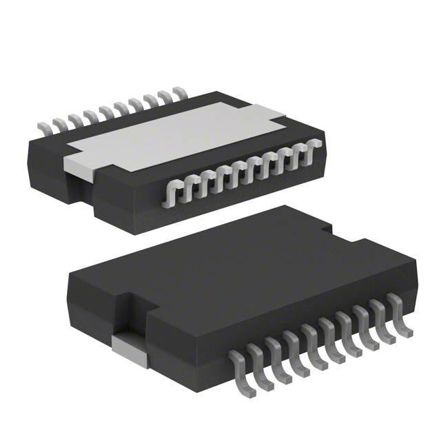
PowerSO-20 PowerSSO24
PowerSO16
Features
Programmable current regulation peak
threshold by SPI up to 8.6 A typ.
Operating battery supply voltage 4.0 V to 28 V
Operating Vdd supply voltage 4.5 V to 5.5 V
All pins withstand 19 V, Vs and output pins
withstand 40 V
Full path Ron from 100 mΩ (at Tj = -40 °C) to
300 mΩ (at Tj =150 °C)
Logic inputs TTL/CMOS-compatible
Operating frequency up to 20 kHz
16-bit SPI interface for
configuration/diagnostics, daisy chain
capability
Over temperature and short circuit protection
VS undervoltage disable function
Vdd undervoltage and overvoltage protection
Vdd overvoltage detection
Open-load detection in ON condition
Full diagnostics in OFF state
Enable and disable input
Low stand by current ( Vs_uv_on
-
0
Vdd over-voltage detection
Although the Vdd input pin and all I/O's are able to withstand up to 19 V, an over-voltage
circuitry is implemented to ensure that the bridge is kept in tri-state when the Vdd voltage is
higher than the Vdd overvoltage threshold "Vdd_ov_off" for duration longer than
"Tov_Vdd". The information is detected and stored into the SPI register in a bit called
"VDD_OV". The bridge is kept in tri-state as long as an appropriate reset is not requested
(see Section 5.1).
Table 14. Vdd over-voltage detection
5.2.8
VDD_OV
Comments
Bridge state
FSI
1
Vdd > Vdd_ov_off
Hi-Z
1 (latched)
0 (default)
Vdd < Vdd_ov_on
-
0
Vdd under-voltage detection
When the Vdd voltage falls below the under-voltage detection threshold "Vdd_uv_off" for
duration longer than "Tuv_vdd", the bridge is switched to tri-state. In such a condition, the
L9958 is going in sleep mode. When the voltage increases above the threshold (hysteresis
implemented), the L9958 starts with all the settings reset to their default values (Power On
Reset).
5.2.9
Output short protection
The L9958 can sustain short on the outputs. In case of short to GND, short to battery or
short between outputs the battery voltage cannot exceed 18 V. The connection of a 100 μF
plus a 1μF decoupling capacitors as close as possible to Vs pin and the GND connection of
the slug or of the exposed pad is mandatory to improve the robustness.
22/38
DocID17269 Rev 6
�L9958
5.3
Diagnostics and protections
Off-state diagnosis
This diagnostic is performed in any off-state condition, just after ignition key-on or during an
off-state phase occurring after an on-state phase of the bridge.
5.3.1
Off-state detection scheme
In order to avoid any wrong diagnostic, a filtering time "Tdiag_off" is applied before
performing the detection if the bridge was in on-state before. This filtering time is not applied
in case of detection after key on.
Figure 18. Off-state detection scheme
0/2
$)
%.
/&&
/.
/&&
/.
4DIAG?OFF
/&&
/.
4DIAG?OFF
/&&
3,%%0
$)!'
30)
$IAG $IAG .O
.O .O .O .O .O $IAG $IAG .O
.O
.O .O .O
.O .O
.O
$ONE $ONE $IAG $IAG $IAG $IAG $IAG $IAG $ONE $ONE $IAG $IAG $IAG $IAG $IAG $IAG $IAG $IAG
'!0'03�����
Open load detection
An equivalent resistor of 100 k (typ.) is targeted for open-load detection.
In order to avoid any unwanted supply of the bridge through the high-side transistor body
diode during off-state measurement, the current source is connected only if Vs is higher
than the Vs under-voltage threshold.
Figure 19. Open load detection
4YPICALVALUE
FORDETECTION
/0%.,/!$
,/!$#/..%#4%$
5.3.2
��K
���K
���K
'!0'03�����
The diagnostic is based on a closed loop voltage control on OUT1 and associated current
measurement.
A voltage amplifier forces a constant voltage on OUT1 through two current sources (highside source and low-side current sink). The OUT2 is pulled-down through a constant current
sink. Based on the current flowing out of the amplifier (Ip – In) compared to several current
thresholds, open-load as well as short-circuit to ground and battery can be detected.
DocID17269 Rev 6
23/38
37
�Diagnostics and protections
L9958
Figure 20. Off-state diagnostic principle
6PS
6PS
�
#URRENT-IRROR
AND#OMPARATOR
)PL
�
)PH
CMD?DIAG
6DD
CMD?DIAG
6DD
)N
6?")!3
�
)N
)?DIAG
,/!$
6DD
37)4#(!
#URRENT-IRROR
AND#OMPARATOR
�
37)4#("
�
#522%.43).+
'!0'03�����
5.4
H-Bridge functional status
Three bits in the diagnosis register are used to give a feedback about the state of the HBridge. Status are Current Limitation (bit 4 "C_LIM"), Temperature Warning (bit 5 "T_WRN")
and Bridge Enable Status (bit 7 "ACT"). Those bits do not report a failure but only a
functional state of the H-bridge that could be useful to change the control strategy mainly in
term of power dissipation.
24/38
DocID17269 Rev 6
�L9958
Electrical specifications
6
Electrical specifications
6.1
Absolute maximum ratings
The component must withstand the overall following stimulus without any damage or latchup. Beyond these values, damage to the component may occur.
Table 15. Absolute maximum ratings
Symbol
Parameter
Test condition
Min.
Max.
Unit
-1
-2
40
40
V
Vps
Supply voltage
Continuous
Transient (0.5 s; I 10 A)
Vdd
Logic supply voltage
0 V < Vps < 40 V
-0.3
19
V
Vddio
SDO supply voltage
0 V < Vps < 40 V
-0.3
19
V
Vi
Logic input voltage
0 V < Vps < 40 V
0 V < Vdd < 19 V
-0.3
19
V
Vo
Logic output voltage
0 V < Vps < 40 V
0 V < Vdd < 18.7V
-0.3
Vddio+0.3
V
±4
-
±2
-
-
-
-
-100
+100
mA
Output pins
(OUTx, VPS) ESD Compliance
EIA/JESD22-A114-B
Input pins
-
ISO 7637 pulses
Cf. standards
-
Latch-up immunity
Jedec standard
Note:
In case of load dump condition, status of device outputs is kept unchanged.
6.2
Thermal data
kV
Table 16. Thermal data
Symbol
Parameter
Test condition
Min.
Max.
Failure condition
-40
OTsd
Lifetime
-40
150
Unit
Tj
Junction temperature
Tstg
Storage temperature
-
-55
150
°C
Tamb
Ambient temperature
0 V < Vps < 40 V
-40
125
°C
Package PowerSO-20
-
1
Package PowerSO16
-
1
Package PowerSSO24
-
2
Rthj-case
Thermal resistance junction to
case(1)
°C
°C/W
1. Guaranteed by design and package characterization.
DocID17269 Rev 6
25/38
37
�Electrical specifications
L9958
Figure 21. Thermal impedance (junction-ambient) of power packages
��
0W33/��ON�S�P
0W33/��ON�S�PTH�ENH�
��
0W3/��ON�S�P
:4(�#�7
��
0W3/��ON�S�PTH�ENH
��
��
��
�
�
������
�����
����
���
�
��
���
����
4IME�S
'!0'03�����
6.3
Range of functionality
Within the range of functionality, all L9958 functionalities have to be guaranteed. All voltages
refers to GND. Currents are positive into and negative out of the specified pin.
Table 17. Range of functionality
Pos.
Symbol
Parameter
FR1
Vps
FR2
dVps/dt
FR3
Vdd
FR4
dVdd/dt
FR5
Vi
FR6
Vddio
SDO output voltage
FR7
fspi
SPI clock frequency
Test condition
Min.
Typ.
Max.
Unit
Supply voltage
-
Vps_uv_off
14
28(1)
V
Supply voltage slew rate
-
-20
-
20
V/μs
Logic supply voltage
-
Vdd_uv_off
5
Vdd_ov_off
V
-
-
0.025(2)
V/μs
-0.3
-
Vdd_ov_off
V
-
3
-
5.5
V
-
-
-
5
MHz
Logic supply voltage slew
rate
Logic input voltage (SDI, See alsoTable 15:
SCLK, NCS, DI, EN, DIR, Absolute maximum
PWM)
ratings.
1. In load dump conditions Vps ranges between 28V and 40V. During load dump, status of device outputs is kept unchanged,
2. To VDD pin are connected 10μF and 10nF (close to the pin) capacitors.
26/38
DocID17269 Rev 6
�L9958
6.4
Electrical specifications
Electrical characteristics
Tcase = -40 °C to 125 °C unless otherwise specified,
Vdd = 4.5 V to 5.5 V unless otherwise specified
Vps = 4 V to 28 V unless otherwise specified
All voltages refer to GND. Currents are positive into and negative out of the specified pin.
6.4.1
Device supply
Table 18. Device supply
Pos.
1.1
1.2
1.3
6.4.2
Symbol
Ips
Iout
Icc
Parameter
Power supply current
Leakage current on output
Logic-supply current
Test condition
Min.
Typ.
Max.
Unit
Vdd < 0.7 V; Vps = 16 V
from -40 °C to 25 °C
-
-
20
μA
Vdd < 0.7 V; Vps = 16 V
at 125 °C
-
-
35
μA
Fpwm = 0, Iout = 0
-
-
20
mA
Bridge in tri-state
-
-
100
μA
Vdd >Vdd_uv_on
FPWM = 0
-
-
5
mA
FPWM = 20 kHz
(Average value)
-
-
5
mA
Min.
Typ.
Max.
Unit
Device supply monitoring
Table 19. Device supply monitoring
Pos.
Symbol
Parameter
Test condition
2.1
Vps_uv_off
Vps under-voltage threshold
Vps decreasing
-
-
4
V
2.2
Vps_uv_on
Vps under-voltage threshold
Vps increasing
-
-
4.5
V
2.3
Vps_uv_hyst
Vps under-voltage hysteresis
-
0.1
-
-
V
2.4
Tuv_vps
Vps under-voltage filtering time
Vps decreasing
1
-
3
μs
2.5
Vdd_uv_off
Vdd under-voltage threshold
Vdd decreasing
3
-
3.7
V
2.6
Vdd_uv_on
Vdd under-voltage threshold
Vdd increasing
3.3
-
4
V
2.7
Vdd_uv_hyst
Vdd under-voltage hysteresis
-
0.1
-
-
V
2.8
Tuv_Vdd
Vdd under-voltage filtering time Vdd decreasing
1
-
4
μs
2.9
Vdd_ov_off
Vdd over-voltage threshold
Vdd increasing
5.8
-
6.8
V
2.10 Vdd-ov_on
Vdd over-voltage threshold
Vdd decreasing
5.5
-
6.5
V
2.11
Vdd over-voltage hysteresis
-
0.1
-
-
V
Vdd over-voltage filtering time
Vdd increasing
60
100
140
μs
Vdd_ov_hyst
2.12 Tov_Vdd
DocID17269 Rev 6
27/38
37
�Electrical specifications
6.4.3
L9958
SPI
Table 20. SPI
Pos.
Symbol
3.1
fspi
3.2
Parameter
Test condition
Clock frequency (50 % duty
cycle)
Tsdo_trans SDO transition speed, 20-80 %
Min.
Typ.
Max.
Unit
-
-
-
5
MHz
Vsdo = 5V, Cload = 50 pF (1)
5
-
30
ns
Vsdo = 5 V, Cload = 150 pF
5
-
50
ns
3.3
Tclh
Minimum time SCLK = HIGH
-
75
-
ns
3.4
Tcll
Minimum time SCLK = LOW
-
75
-
ns
3.5
Tpcld
Propagation delay (SCLK to
data at 10% of SDO rising edge)
-
-
40
ns
3.6
Tcsdv
NCS = LOW to data at SDO
active
-
-
-
85
ns
3.7
Tsclch
SCLK low before NCS low
(setup time SCLK to NCS
change H/L)
-
75
-
-
ns
3.8
Thclcl
SCLK change L/H after NCS =
low
-
75
-
-
ns
3.9
Tscld
SDI input setup time (SCLK
change H/L after SDI data valid)
40
-
-
ns
3.10
Thcld
SDI input hold time (SDI data
hold after SCLK change H/L)
-
40
-
-
ns
3.11
Tsclcl
SCLK low before NCS high
-
100
-
-
ns
3.12
Thclch
SCLK high after NCS high
-
100
-
-
ns
3.13
Tpchdz
NCS L/H to SDO @ high
impedance
-
-
-
75
ns
3.14
Tonncs
NCS min. high time
-
300
-
3.15
ns
-
Capacitance at SDI, SCLK; NCS -
-
-
14
pF
-
Capacitance at SDO
-
-
-
19
pF
3.16
Tfncs
NCS Filter time will be ignored)
Guaranteed by design
(Pulses = TfNCS
Guaranteed by design
10
-
40
ns
3.17
Vddio
Supply voltage for SDO output
buffer
-
3
-
5.5
V
3.18
Ivddio
Current consumption on Vddio
(2)
-
-
1
mA
3.19
sdo_H
High output level on SDO
Isdo = 1.5 mA
Vddio0.4
-
-
V
3.20
sdo_L
Low output level on SDO
Isdo = 2 mA
-
-
0.4
V
3.21
Isdo
Tri state leakage current
NCS = HIGH VDDIO = 5 V
-5
-
5
μA
1. Not tested – guaranteed by Cload = 150 pF measurement
2. Measured for PSO16 at wafer sort level only.
28/38
DocID17269 Rev 6
�L9958
Electrical specifications
6.4.4
Digital inputs: TTL // 3.3V / 5V CMOS compatible
Table 21. Digital inputs: TTL // 3.3V / 5V CMOS compatible
Pos.
Symbol
4.1
Vih
Input voltage HIGH
4.2
Vil
4.3
Parameter
Test condition
Min.
Typ.
Max.
Unit
-
2
-
Vdd+0.3
V
Input voltage LOW
-
-0.3
-
0.8
V
Hysteresis of input voltage
-
200
-
-
mV
Vin = 0 V
-100
-
-30
-
-
5
30
-
100
-5
-
-
-
-
1.24
-
V
-
-
10
-
kΩ
Overall tolerance can
be taken as 3.5 %
-
1
-
%
Min.
Typ.
Max.
Tj = 150 °C, Iout = 3 A
4 V < Vps < 5 V
-
-
300
Tj = 150 °C, Iout = 3 A
Vps > 5 V
-
-
150
Tj = 150 °C, Iout = 3 A
4 V < Vps < 5 V
-
-
300
Tj = 150 °C, Iout = 3 A
Vps > 5 V
-
-
150
4.4
Iinl
Input current source for: DI /
NCS / SCLK / SDI
4.5
Iinh
Input current sink for: EN / DIR / Vin = 5 V
PWM
Vin = 0 V
Vin = 5 V No back
supply allowed
Vrext
4.6
6.4.5
Rext
External resistor
μA
μA
Bridge output drivers
Table 22. Bridge output drivers
Pos.
5.1
5.2
Symbol
Rdson_h
Rdson_l
Parameter
Test condition
High-side transistor Rdson
Low-side transistor Rdson
Unit
mΩ
mΩ
5.3
Vbd_h
Body diode forward voltage
drop high-side transistor
Idiode = 3 A
-
1.2
2
V
5.4
Vbd_l
Body diode forward voltage
drop low-side transistor
Idiode = 3 A
-
1.2
2
V
DocID17269 Rev 6
29/38
37
�Electrical specifications
6.4.6
L9958
Over-temperature monitoring
Table 23. Over-temperature monitoring
Pos.
Symbol
6.1
OTwarn
6.2
Parameter
Test condition
Min.
Typ.
Max.
Unit
Over-temperature warning
-
150
-
170
°C
OTsd
Over-temperature shut-down
-
170
-
200
°C
6.3
OThyst
Over-temperature hysteresis
-
10
-
-
°C
6.4
TTSD
Over-temperature filtering time
Guaranteed by clock
measurement
-
36
-
μs
Unit
6.4.7
Current limitation and over-current detection
Table 24. Current limitation and over-current detection
Pos.
7.1
Symbol
Ilim_H
Parameter
Current limitation high
threshold
Test condition
Min.
Typ.
Max.
CL1:0 = 00; -40 °C ≤ Tj ≤ 150 °C
2
2.5
3.1
CL1:0 = 01; -40 °C ≤ Tj ≤ 150 °C
3.5
4
4.85
CL1:0 = 10; -40 °C ≤ Tj < 25 °C
5.5
6.75
8
CL1:0 = 10; 25 °C ≤ Tj ≤ 150 °C
5.5
6.6
7.7
CL1:0 = 11; -40 °C ≤ Tj < 25 °C
7.8
9.1
10.4
CL1:0 = 11; 25 °C ≤ Tj ≤ 150°C
7.6
8.6
9.6
2
2.5
3
Ilim_H–0.2
Ilim_H0.5
Ilim_H0.8
CL1:0 = 10; -40°C ≤ Tj < 25 °C
Ilim_H–
0.35
Ilim_H0.65
Ilim_H0.95
CL1:0 = 10; 25 °C ≤ Tj ≤ 150°C
Ilim_H–
0.35
Ilim_H0.55
Ilim_H0.85
CL1:0 = 11; -40°C ≤ Tj < 25°C
Ilim_H–0.4
Ilim_H0.7
Ilim_H-1
CL1:0 = 11; 25 °C ≤ Tj ≤ 150°C
Ilim_H–0.4
Ilim_H0.55
Ilim_H0.95
0.1
-
1
μs
CL1:0 = XX, Tj = OTsd
CL1:0 = 0X; -40 °C ≤ Tj ≤ 150 °C
7.2
Ilim_L
Current limitation low
threshold
A
A
7.3
Tlimh
High current limitation
threshold filtering time
can be included in Tblanck
7.4
Tliml
Low current limitation
threshold filtering time
-
1
-
3
μs
7.5
Toffmin
Current limitation delay
time
30
-
45
μs
7.6
Tb
Blanking time
4.9
-
8.7
μs
30/38
-
DocID17269 Rev 6
�L9958
Electrical specifications
Table 24. Current limitation and over-current detection (continued)
Pos.
Symbol
Ioc_ls
Ioc-hs
7.7
Tracking
Parameter
Low-side over-current
threshold
High-side over-current
threshold
Test condition
Min.
Typ.
Max.
CL1:0 = 0X; -40 °C ≤ Tj ≤ 150 °C
5.5
7.7
11
CL1:0 = 1X; -40°C ≤ Tj < 25 °C
9.3
12
16.5
CL1:0 = 1X; 25 °C ≤ Tj ≤ 150°C
9.3
11.5
14
Ilim_h+2
-
-
Ilim_h+1.3
-
-
0.8
-
2.5
μs
Unit
CL1:0 = 0X; CL1:0 = 10;
-40 °C ≤ Tj ≤ 150 °C
CL1:0 = 11; -40 °C ≤ Tj ≤ 150 °C
7.8
6.4.8
Toc_ls
Toc_hs
Low-side & high-side
over-current detection
filtering time
-
Unit
A
Diagnostic of open-load in on-state
Table 25. Diagnostic of open-load in on-state
Pos.
Symbol
Parameter
Test condition
Tj = -40 °C (go-no-go
functional test)
8.1
8.2
6.4.9
Is_OL-on
Current source
Tj = 25 °C to 150 °C
(go-no-go functional
test)
Min.
Typ.
Max.
50
-
120
μA
50
-
100
-
3
5
μs
Min.
Typ.
Max.
Unit
Load detection threshold
10
60
200
k
Tmeas_on Detection time (settling time)
-
Off-state diagnostic
Table 26. Off-state diagnostic
Pos.
Symbol
9.1
ROL
9.2
Tdiag_off
diag after on-state
Delay time before enabling offGuaranteed through
state diagnostic structure
SCAN
100
125
150
ms
Tdiag-off_1
used each time OUT
pins are released from
Off-state diag filtering time
Vps (after release of
when OUT 1 and/or 2 decrease
SCB, after Tdiag_off)
from Vps
Guaranteed through
SCAN
2.4
3
3.6
ms
9.4
Tdiag_off_2
Off-state diagnostic filtering
time on failure detection
One symmetric filter for
each failure type (OL,
SCG, SCB) Guaranteed
through SCAN
200
250
300
μs
9.5
Tclock
Oscillator frequency
-
4
-
6
MHz
9.3
Parameter
Test condition
DocID17269 Rev 6
31/38
37
�Electrical specifications
6.4.10
L9958
Timing characteristics
Table 27. Timing characteristics
Pos.
Symbol
10.1
fpwm
PWM frequency
Tdon
10.2
Parameter
Test condition
Min.
Typ.
Max.
Unit
-
-
-
20
kHz
Delay time for switch-on
Rload @ Iout = 3 A
PWM → 90% Vout (or
10 % Iout)
-
-
10
μs
Tdoff
Delay time for switch-off
Rload @ Iout = 3 A
PWM → 10 % Vout (or
90% Iout)
-
-
10
μs
Td
Delay time: symmetry
PWM accuracy = 1% @
2kHz
-
-
5
μs
10.3
Td_dis
Disable delay time
DI / EN → 90% OUTx
@ Iout = 3 A
-
-
6
μs
10.4
Td_en
Enable delay time
DI / EN → 10 % OUT
-
-
6
μs
-
-
200
μs
1
-
3
μs
10.5
Td_pow
Power-on delay time
DIR= PWM=EN=1 /
DI=0 no load / VPS =
Vdd increasing
Vps = Vdd → 10 % Vout1
(= Vps)
10.6
Td_filter
DI / EN digital filter time
-
10.7
Trise_H
Low-side transistor rise time
Non selectable by SPI
0.04
-
0.2
μs
10.8
Tfall_H
Low-side transistor fall time
Non selectable by SPI
1
-
3
μs
7
14
24
dVout/dt
Voltage slew rate for high-side super fast mode
transistors
VSR = 0
(Measurement is performed
between 30 % and 70 % of the
VSR = 1
slope)
2
4
6
1
2
3
1.5
3
4.5
0.15
0.3
0.45
35
-
55
10.9
10.10
dIout/dt
10.11
Tdiag
32/38
Current slew rate for high-side ISR=0
transistors
(Measurement is performed
between 40 % and 60 % of the ISR=1
slope)
Timing for reliable diagnostic
Guaranteed through
SCAN pattern
DocID17269 Rev 6
V/μs
A/μs
μs
�L9958
7
Application circuit
Application circuit
Figure 22. Application circuit
"!44%29
��6
���N&
#0
���&
�&
63
6$$
�6
0OWER3UPPLY
�6����6
���N&
��K7
$)
%.
/54�
07$)2
#
���N&
��K7
6$$)/
��N&
$#
,����
��&
.#3
/54�
3#+
��N&
3)
3/
2%84
��K7
'.$S
'!0'03�����
1. The above application diagram shows all the suggested components for a proper device operation.
DocID17269 Rev 6
33/38
37
�Package information
8
L9958
Package information
In order to meet environmental requirements, ST offers these devices in different grades of
ECOPACK® packages, depending on their level of environmental compliance. ECOPACK®
specifications, grade definitions and product status are available at: www.st.com.
ECOPACK® is an ST trademark.
Figure 23. PowerSO-20 mechanical data and package dimensions
$)-�
MM
-).�
490�
!
A�
INCH
-!8�
-).�
490�
���
���
�����
���
A�
�����
�����
���
A�
�����
�
���
�����
�����
B
���
����
�����
�����
C
����
����
�����
�����
$��
����
��
�����
�����
$���
���
���
�����
�����
%
����
����
�����
E
����
E�
%���
%�
�����
�����
����
%�
�����
�����
�����
�����
���
���
�����
���
'
�
���
�����
�����
(
����
����
�����
�����
���
���
�����
�����
H
,
���
�����
.
� �TYP�
3
� �MAX�
4
7EIGHT����GR
�����
�����
����
/54,).%!.$
-%#(!.)#!,$!4!
-!8�
��
*%$%#-/
���
�����
0OWER3/��
�� h$AND%�vDONOTINCLUDEMOLDFLASHORPROTUSIONS�
-OLDFLASHORPROTUSIONSSHALLNOTEXCEED����MM������v
#RITICALDIMENSIONS�h%v�h'vANDhA�v�
�� &ORSUBCONTRACTORS�THELIMITISTHEONEQUOTEDINJEDEC-/
���
.
2
.
A�
B
!
E
$%4!),!
C
A�
$%4!),"
%
E�
(
$%4!),!
LEAD
$
SLUG
A�
$%4!),"
��
��
����
'AGE0LANE
#
3
3%!4).'0,!.%
,
'
%�
%�
"/44/-6)%7
#
�#/0,!.!2)49
4
%�
�
HX��
�
�
03/��-%#
$�
�������)
'!0'03�����
34/38
DocID17269 Rev 6
�L9958
Package information
Figure 24. PowerSO16 mechanical data and package dimensions
$)-�
-).�
�
���
���
����
!�
!�
!�
!�
A
B
C
$
$�
D
%��
%�
%�
%�
E
E�
&
'
,
2�
2�
4
4�
4�
����
����
���
���
�����
���
���
���
���
MM
490�
����
���
���
���
���
����
����
���
���
���
����
���
���
���
���
���
���
���
����
-!8�
���
���
���
����
-).�
�
�����
�����
�����
����
����
���
���
�����
�����
����
�����
�����
���
���
���
�����
�����
�����
�����
���
����
�����
INCH
490�
�����
�����
����
�����
�����
�����
����
�����
�����
�����
�����
����
�����
����
�����
����
�����
�����
�����
/54,).%!.$
-%#(!.)#!,$!4!
-!8�
�����
�����
�����
����
�����
�����
�����
�����
�����
�����
�����
�����
�����
����
���
�����
���PLQ�������W\S�������PD[��
���W\S��
����W\S��
0OWER3/��
�� 2ESINPROTRUSIONSNOTINCLUDED�MAXVALUE����MMPERSIDE �
B
,
A
-
, - #
5
��
4�
�
4�
&
'
-
%�
%
�
%�
2�
�
%�
2�
E
E�
3%4$%4!),+
$
$�
4�
3%4$%4!),+
$%4!),*
4
2�
!�
#
!�
2�
!�
!�
4�
3%%$%4!),*
3%!4).'
0,!.%
D #
,EADSCOPLANARITY
,
'!5'%0,!.%
����
03/��-%#
'!0'03�����
DocID17269 Rev 6
35/38
37
�Package information
L9958
Figure 25. PowerSSO24 mechanical data and package dimensions
$IM�
!
!�
A�
B
C
$��
%��
E�
E�
&�
'
'�
(
H
K
,
/
1
3
4
5
.
8
9
-IN�
MM
4YP�
����
�
����
����
�����
����
-AX�
����
����
����
����
����
�����
�����
�
�����
�����
�����
����
�����
���
����
���
����
-AX�
������
������
�����
�����
�����
�����
/54,).%!.$
-%#(!.)#!,$!4 !
�����
�����
�����
�����
����
����
����� �����
����
���PLQ�������PD[��
���� ������
�����
����
����
����
����
���
����
����
������
INCH
4YP�
-IN�
����PD[�
���� �����
���� �����
������ �������
�����
�����
�����
�����
������
�����
�����
�����
�����
�����
�����
�����
�������
�� h$AND%�vDONOTINCLUDEMOLDFLASHORPROTUSIONS�
-OLDFLASHORPROTUSIONSSHALLNOTEXCEED����MM������v
�� .OINTRUSIONALLOWEDINWARDSTHELEADS�
�� &LASHORBLEEDSONEXPOSEDDIEPADSHALLNOTEXCEED���MMPERSIDE
�� 6A RIATIONFORSMALLWINDOWLEADFRAMEOPTION�
0OWER33/��
�%XPOSEDPADDOWN
�������*
'!0'03�����
36/38
DocID17269 Rev 6
�L9958
9
Revision history
Revision history
Table 28. Document revision history
Date
Revision
Changes
16-Mar-2010
1
Initial release.
08-Apr-2011
2
Updated Table 27: Timing characteristics on page 32 (Pos. 10.8).
03-Aug-2011
3
Updated Table 17, Table 20, Table 24 and Table 27.
23-Mar-2012
4
Updated:
Table 17: Range of functionality;
Table 20: SPI.
19-Sep-2013
5
Updated disclaimer.
05-Dec-2013
6
Updated Table 24: Current limitation and over-current detection pag
31.
DocID17269 Rev 6
37/38
37
�L9958
Please Read Carefully:
Information in this document is provided solely in connection with ST products. STMicroelectronics NV and its subsidiaries (“ST”) reserve the
right to make changes, corrections, modifications or improvements, to this document, and the products and services described herein at any
time, without notice.
All ST products are sold pursuant to ST’s terms and conditions of sale.
Purchasers are solely responsible for the choice, selection and use of the ST products and services described herein, and ST assumes no
liability whatsoever relating to the choice, selection or use of the ST products and services described herein.
No license, express or implied, by estoppel or otherwise, to any intellectual property rights is granted under this document. If any part of this
document refers to any third party products or services it shall not be deemed a license grant by ST for the use of such third party products
or services, or any intellectual property contained therein or considered as a warranty covering the use in any manner whatsoever of such
third party products or services or any intellectual property contained therein.
UNLESS OTHERWISE SET FORTH IN ST’S TERMS AND CONDITIONS OF SALE ST DISCLAIMS ANY EXPRESS OR IMPLIED
WARRANTY WITH RESPECT TO THE USE AND/OR SALE OF ST PRODUCTS INCLUDING WITHOUT LIMITATION IMPLIED
WARRANTIES OF MERCHANTABILITY, FITNESS FOR A PARTICULAR PURPOSE (AND THEIR EQUIVALENTS UNDER THE LAWS
OF ANY JURISDICTION), OR INFRINGEMENT OF ANY PATENT, COPYRIGHT OR OTHER INTELLECTUAL PROPERTY RIGHT.
ST PRODUCTS ARE NOT DESIGNED OR AUTHORIZED FOR USE IN: (A) SAFETY CRITICAL APPLICATIONS SUCH AS LIFE
SUPPORTING, ACTIVE IMPLANTED DEVICES OR SYSTEMS WITH PRODUCT FUNCTIONAL SAFETY REQUIREMENTS; (B)
AERONAUTIC APPLICATIONS; (C) AUTOMOTIVE APPLICATIONS OR ENVIRONMENTS, AND/OR (D) AEROSPACE APPLICATIONS
OR ENVIRONMENTS. WHERE ST PRODUCTS ARE NOT DESIGNED FOR SUCH USE, THE PURCHASER SHALL USE PRODUCTS AT
PURCHASER’S SOLE RISK, EVEN IF ST HAS BEEN INFORMED IN WRITING OF SUCH USAGE, UNLESS A PRODUCT IS
EXPRESSLY DESIGNATED BY ST AS BEING INTENDED FOR “AUTOMOTIVE, AUTOMOTIVE SAFETY OR MEDICAL” INDUSTRY
DOMAINS ACCORDING TO ST PRODUCT DESIGN SPECIFICATIONS. PRODUCTS FORMALLY ESCC, QML OR JAN QUALIFIED ARE
DEEMED SUITABLE FOR USE IN AEROSPACE BY THE CORRESPONDING GOVERNMENTAL AGENCY.
Resale of ST products with provisions different from the statements and/or technical features set forth in this document shall immediately void
any warranty granted by ST for the ST product or service described herein and shall not create or extend in any manner whatsoever, any
liability of ST.
ST and the ST logo are trademarks or registered trademarks of ST in various countries.
Information in this document supersedes and replaces all information previously supplied.
The ST logo is a registered trademark of STMicroelectronics. All other names are the property of their respective owners.
© 2013 STMicroelectronics - All rights reserved
STMicroelectronics group of companies
Australia - Belgium - Brazil - Canada - China - Czech Republic - Finland - France - Germany - Hong Kong - India - Israel - Italy - Japan Malaysia - Malta - Morocco - Philippines - Singapore - Spain - Sweden - Switzerland - United Kingdom - United States of America
www.st.com
38/38
DocID17269 Rev 6
�


 工商网监
湘ICP备2023018690号
工商网监
湘ICP备2023018690号
