APT1204R7BFLL
APT1204R7SFLL
1200V 3.5A 4.700Ω
POWER MOS 7
R
FREDFET
D3PAK
®
Power MOS 7 is a new generation of low loss, high voltage, N-Channel
enhancement mode power MOSFETS. Both conduction and switching
®
losses are addressed with Power MOS 7 by significantly lowering RDS(ON)
®
and Qg. Power MOS 7 combines lower conduction and switching losses
along with exceptionally fast switching speeds inherent with Microsemi's
patented metal gate structure.
• Lower Input Capacitance
• Lower Miller Capacitance
• Lower Gate Charge, Qg
VDSS
D
• Increased Power Dissipation
• Easier To Drive
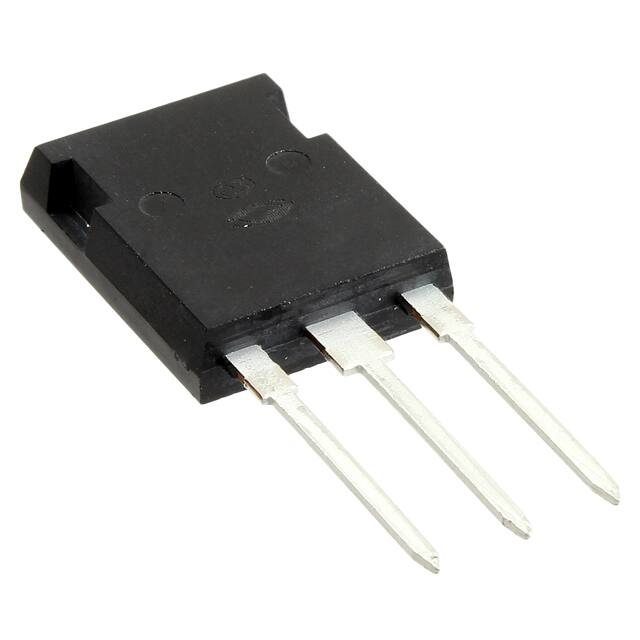
• TO-247 or Surface Mount D3PAK Package
MAXIMUM RATINGS
Symbol
TO-247
G
S
All Ratings: TC = 25°C unless otherwise specified.
Parameter
APT1204R7B_SFLL
UNIT
1200
Volts
Drain-Source Voltage
ID
Continuous Drain Current @ TC = 25°C
IDM
Pulsed Drain Current
VGS
Gate-Source Voltage Continuous
±30
VGSM
Gate-Source Voltage Transient
±40
Total Power Dissipation @ TC = 25°C
135
Watts
Linear Derating Factor
1.08
W/°C
PD
TJ,TSTG
1
Operating and Storage Junction Temperature Range
Lead Temperature: 0.063" from Case for 10 Sec.
IAR
Avalanche Current
EAR
Repetitive Avalanche Energy
1
Amps
14
TL
EAS
3.5
-55 to 150
°C
300
Amps
3.5
(Repetitive and Non-Repetitive)
1
Single Pulse Avalanche Energy
Volts
10
4
mJ
425
STATIC ELECTRICAL CHARACTERISTICS
RDS(on)
IDSS
IGSS
VGS(th)
MIN
Drain-Source Breakdown Voltage (VGS = 0V, ID = 250µA)
1200
Drain-Source On-State Resistance
2
(VGS = 10V, ID = 1.75A)
TYP
MAX
UNIT
Volts
4.70
Ohms
Zero Gate Voltage Drain Current (VDS = 1200V, VGS = 0V)
250
Zero Gate Voltage Drain Current (VDS = 960V, VGS = 0V, TC = 125°C)
1000
Gate-Source Leakage Current (VGS = ±30V, VDS = 0V)
±100
nA
5
Volts
Gate Threshold Voltage (VDS = VGS, ID = 1mA)
3
CAUTION: These Devices are Sensitive to Electrostatic Discharge. Proper Handling Procedures Should Be Followed.
Microsemi Website - http://www.microsemi.com
µA
7-2006
BVDSS
Characteristic / Test Conditions
050-7390 Rev B
Symbol
�APT1204R7B_SFLL
DYNAMIC CHARACTERISTICS
Symbol
C iss
Characteristic
Test Conditions
Input Capacitance
Coss
VGS = 0V
Output Capacitance
VDS = 25V
C rss
Reverse Transfer Capacitance
f = 1 MHz
Qg
Total Gate Charge
Qgs
Gate-Source Charge
Qgd
Gate-Drain ("Miller ") Charge
td(on)
Turn-on Delay Time
tr
3
RESISTIVE SWITCHING
VGS = 15V
VDD = 600V
ID = 3.5A @ 25°C
Turn-on Switching Energy
Eoff
Turn-off Switching Energy
INDUCTIVE SWITCHING @ 25°C
6
Eon
Turn-on Switching Energy
Eoff
Turn-off Switching Energy
ns
115
VDD = 800V, VGS = 15V
23
ID = 3.5A, RG = 5Ω
INDUCTIVE SWITCHING @ 125°C
6
nC
24
RG = 1.6Ω
Eon
UNIT
pF
36
31
4
21
7
2
20
VDD = 600V
Fall Time
MAX
715
130
ID = 3.5A @ 25°C
Turn-off Delay Time
tf
TYP
VGS = 10V
Rise Time
td(off)
MIN
µJ
135
VDD = 800V, VGS = 15V
ID = 3.5A, RG = 4.3Ω
25
SOURCE-DRAIN DIODE RATINGS AND CHARACTERISTICS
Characteristic / Test Conditions
Symbol
MIN
TYP
MAX
UNIT
IS
Continuous Source Current (Body Diode)
ISM
Pulsed Source Current
1
(Body Diode)
14
VSD
Diode Forward Voltage
2
(VGS = 0V, IS = -ID 3.5A)
1.3
Volts
dv/
Peak Diode Recovery
18
V/ns
dt
dv/
dt
3.5
5
t rr
Reverse Recovery Time
(IS = -ID 3.5A, di/dt = 100A/µs)
Tj = 25°C
250
Tj = 125°C
515
Q rr
Reverse Recovery Charge
(IS = -ID 3.5A, di/dt = 100A/µs)
Tj = 25°C
0.5
Tj = 125°C
1.1
IRRM
Peak Recovery Current
(IS = -ID 3.5A, di/dt = 100A/µs)
Tj = 25°C
8.3
Tj = 125°C
11.5
Amps
ns
µC
Amps
THERMAL CHARACTERISTICS
Symbol
Characteristic
MIN
TYP
MAX
0.90
RθJC
Junction to Case
RθJA
Junction to Ambient
40
1 Repetitive Rating: Pulse width limited by maximum junction
temperature
2 Pulse Test: Pulse width < 380 µs, Duty Cycle < 2%
3 See MIL-STD-750 Method 3471
0.9
0.7
0.60
0.5
Note:
0.40
PDM
Z JC, THERMAL IMPEDANCE (°C/W)
θ
050-7390 Rev B
7-2006
1.0
0.3
SINGLE PULSE
0.20
0.1
0
t1
t2
Duty Factor D = t1/t2
Peak TJ = PDM x ZθJC + TC
0.05
10-5
10-4
°C/W
4 Starting Tj = +25°C, L = 69.39mH, RG = 25Ω, Peak IL = 3.5A
5 dv/dt numbers reflect the limitations of the test circuit rather than the
device itself. IS ≤ -ID3.5A di/dt ≤ 700A/µs VR ≤ 1200 TJ ≤ 150°C
6 Eon includes diode reverse recovery. See figures 18, 20.
Microsemi reserves the right to change, without notice, the specifications and information contained herein.
0.80
UNIT
10-3
10-2
10-1
RECTANGULAR PULSE DURATION (SECONDS)
FIGURE 1, MAXIMUM EFFECTIVE TRANSIENT THERMAL IMPEDANCE, JUNCTION-TO-CASE vs PULSE DURATION
1.0
�Typical Performance Curves
0.386
0.508
Dissipated Power
(Watts)
0.0903
ZEXT are the external thermal
impedances: Case to sink,
sink to ambient, etc. Set to
zero when modeling only
the case to junction.
ID, DRAIN CURRENT (AMPERES)
TC ( C)
ZEXT
TJ ( C)
0.00336
8
6
TJ = -55°C
TJ = +125°C
4
TJ = +25°C
2
0
1
2
3
4
5
6
7
8
VGS, GATE-TO-SOURCE VOLTAGE (VOLTS)
FIGURE 4, TRANSFER CHARACTERISTICS
3
2.5
2
1.5
1
0.5
25
4
6V
3
2
5.5V
1
5V
1.40
V
NORMALIZED TO
= 10V @ 1.75A
GS
1.30
1.20
VGS=10V
1.10
1.00
VGS=20V
0.90
0.80
0
1
2
3
4
5
6
ID, DRAIN CURRENT (AMPERES)
FIGURE 5, RDS(ON) vs DRAIN CURRENT
D
V
1.05
1.00
0.95
0.90
0.85
-50
1.2
= 1.75A
GS
= 10V
2.0
1.5
1.0
0.5
-50 -25
0
25 50
75 100 125 150
TJ, JUNCTION TEMPERATURE (°C)
FIGURE 8, ON-RESISTANCE vs. TEMPERATURE
1.1
1.0
0.9
0.8
7-2006
I
1.10
-25
0
25
50 75 100 125 150
TJ, JUNCTION TEMPERATURE (°C)
FIGURE 7, BREAKDOWN VOLTAGE vs TEMPERATURE
VGS(TH), THRESHOLD VOLTAGE
(NORMALIZED)
RDS(ON), DRAIN-TO-SOURCE ON RESISTANCE
(NORMALIZED)
50
75
100
125
150
TC, CASE TEMPERATURE (°C)
FIGURE 6, MAXIMUM DRAIN CURRENT vs CASE TEMPERATURE
2.5
0.0
6.5V
1.15
BVDSS, DRAIN-TO-SOURCE BREAKDOWN
VOLTAGE (NORMALIZED)
ID, DRAIN CURRENT (AMPERES)
3.5
0
5
0.7
0.6
-50 -25
0
25
50
75 100 125 150
TC, CASE TEMPERATURE (°C)
FIGURE 9, THRESHOLD VOLTAGE vs TEMPERATURE
050-7390 Rev B
0
7V
6
0
5
10
15
20
25
30
VDS, DRAIN-TO-SOURCE VOLTAGE (VOLTS)
FIGURE 3, LOW VOLTAGE OUTPUT CHARACTERISTICS
RDS(ON), DRAIN-TO-SOURCE ON RESISTANCE
ID, DRAIN CURRENT (AMPERES)
VDS> ID (ON) x RDS (ON)MAX.
250 µSEC. PULSE TEST
@