APT30M60J
600V, 31A, 0.15Ω Max
N-Channel MOSFET
S
S
Power MOS 8™ is a high speed, high voltage N-channel switch-mode power MOSFET.
A proprietary planar stripe design yields excellent reliability and manufacturability. Low
switching loss is achieved with low input capacitance and ultra low Crss "Miller" capacitance. The intrinsic gate resistance and capacitance of the poly-silicon gate structure
help control slew rates during switching, resulting in low EMI and reliable paralleling,
even when switching at very high frequency. Reliability in flyback, boost, forward, and
other circuits is enhanced by the high avalanche energy capability.
D
G
SO
2
T-
27
"UL Recognized"
file # E145592
IS OTO P ®
D
APT30M60J
Single die MOSFET
G
S
TYPICAL APPLICATIONS
FEATURES
• Fast switching with low EMI/RFI
• PFC and other boost converter
• Low RDS(on)
• Buck converter
• Ultra low Crss for improved noise immunity
• Two switch forward (asymmetrical bridge)
• Low gate charge
• Single switch forward
• Avalanche energy rated
• Flyback
• RoHS compliant
• Inverters
Absolute Maximum Ratings
Symbol
ID
Parameter
Unit
Ratings
Continuous Drain Current @ TC = 25°C
31
Continuous Drain Current @ TC = 100°C
19
A
IDM
Pulsed Drain Current
VGS
Gate-Source Voltage
±30
V
EAS
Single Pulse Avalanche Energy 2
1200
mJ
IAR
Avalanche Current, Repetitive or Non-Repetitive
21
A
1
160
Thermal and Mechanical Characteristics
Min
Typ
Max
Unit
W
PD
Total Power Dissipation @ TC = 25°C
355
RθJC
Junction to Case Thermal Resistance
0.35
RθCS
Case to Sink Thermal Resistance, Flat, Greased Surface
TJ,TSTG
Operating and Storage Junction Temperature Range
VIsolation
RMS Voltage (50-60hHz Sinusoidal Waveform from Terminals to Mounting Base for 1 Min.)
WT
Torque
Package Weight
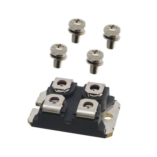
Terminals and Mounting Screws.
Microsemi Website - http://www.microsemi.com
°C/W
0.15
-55
150
°C
V
2500
1.03
oz
29.2
g
10
in·lbf
1.1
N·m
Rev C 7-2011
Characteristic
050-8078
Symbol
�Static Characteristics
TJ = 25°C unless otherwise specified
Symbol
Parameter
Test Conditions
Min
VBR(DSS)
Drain-Source Breakdown Voltage
VGS = 0V, ID = 250μA
600
∆VBR(DSS)/∆TJ
Drain-Source On Resistance
VGS(th)
Gate-Source Threshold Voltage
∆VGS(th)/∆TJ
VGS = 10V, ID = 21A
3
Zero Gate Voltage Drain Current
IGSS
Gate-Source Leakage Current
Dynamic Characteristics
Forward Transconductance
Ciss
Input Capacitance
Crss
Reverse Transfer Capacitance
Coss
Output Capacitance
VDS = 600V
TJ = 25°C
VGS = 0V
TJ = 125°C
Typ
Max
0.57
0.12
4
-10
0.15
5
100
500
±100
VGS = ±30V
Unit
V
V/°C
Ω
V
mV/°C
μA
nA
TJ = 25°C unless otherwise specified
Parameter
gfs
3
VGS = VDS, ID = 2.5mA
Threshold Voltage Temperature Coefficient
IDSS
Symbol
Reference to 25°C, ID = 250μA
Breakdown Voltage Temperature Coefficient
RDS(on)
APT30M60J
Min
Test Conditions
VDS = 50V, ID = 21A
4
Effective Output Capacitance, Charge Related
Co(er)
5
Effective Output Capacitance, Energy Related
Max
42
5890
90
800
VGS = 0V, VDS = 25V
f = 1MHz
Co(cr)
Typ
Unit
S
pF
420
VGS = 0V, VDS = 0V to 400V
220
Qg
Total Gate Charge
Qgs
Gate-Source Charge
Qgd
Gate-Drain Charge
td(on)
Turn-On Delay Time
Resistive Switching
Current Rise Time
VDD = 400V, ID = 21A
tr
td(off)
tf
Turn-Off Delay Time
215
45
90
48
55
145
44
VGS = 0 to 10V, ID = 21A,
VDS = 300V
RG = 4.7Ω 6 , VGG = 15V
Current Fall Time
nC
ns
Source-Drain Diode Characteristics
Symbol
IS
ISM
Parameter
Continuous Source Current
(Body Diode)
Pulsed Source Current
(Body Diode) 1
Test Conditions
MOSFET symbol
showing the
integral reverse p-n
junction diode
(body diode)
Diode Forward Voltage
ISD = 21A, TJ = 25°C, VGS = 0V
trr
Reverse Recovery Time
ISD = 21A 3
Qrr
Reverse Recovery Charge
Peak Recovery dv/dt
Typ
Max
Unit
31
A
G
VSD
dv/dt
Min
D
160
S
diSD/dt = 100A/μs, TJ = 25°C
ISD ≤ 21A, di/dt ≤1000A/μs, VDD = 400V,
TJ = 125°C
1.0
705
15.2
V
ns
μC
8
V/ns
1 Repetitive Rating: Pulse width and case temperature limited by maximum junction temperature.
2 Starting at TJ = 25°C, L = 5.44mH, RG = 4.7Ω, IAS = 21A.
050-8078
Rev C
7-2011
3 Pulse test: Pulse Width < 380μs, duty cycle < 2%.
4 Co(cr) is defined as a fixed capacitance with the same stored charge as COSS with VDS = 67% of V(BR)DSS.
5 Co(er) is defined as a fixed capacitance with the same stored energy as COSS with VDS = 67% of V(BR)DSS. To calculate Co(er) for any value of
VDS less than V(BR)DSS, use this equation: Co(er) = -8.32E-8/VDS^2 + 3.49E-8/VDS + 1.30E-10.
6 RG is external gate resistance, not including internal gate resistance or gate driver impedance. (MIC4452)
Microsemi reserves the right to change, without notice, the specifications and information contained herein.
�APT30M60J
160
V
GS
70
= 10V
120
100
TJ = 25°C
80
60
40
50
6V
40
30
20
5.5V
TJ = 125°C
0
0
5
10
15
20
25
30
VDS(ON), DRAIN-TO-SOURCE VOLTAGE (V)
5V
4.5V
0
Figure 2, Output Characteristics
160
NORMALIZED TO
VGS = 10V @ 21A
2.5
2.0
1.5
1.0
0.5
250μSEC. PULSE TEST
@ ID(ON) x RDS(ON) MAX.
140
ID, DRAIN CURRENT (A)
RDS(ON), DRAIN-TO-SOURCE ON RESISTANCE
Figure 1, Output Characteristics
3.0
5
10
15
20
25
30
VDS, DRAIN-TO-SOURCE VOLTAGE (V)
050-8078
0
GS
10
TJ = 150°C
20
= 7&8V
V
J
60
ID, DRIAN CURRENT (A)
ID, DRAIN CURRENT (A)
T = 125°C
TJ = -55°C
140
�APT30M60J
200
200
100
100
IDM
10
ID, DRAIN CURRENT (A)
ID, DRAIN CURRENT (A)
IDM
13μs
100μs
1ms
10ms
Rds(on)
1
100ms
DC line
0.1
13μs
Rds(on)
TJ = 150°C
TC = 25°C
1
100μs
1ms
10ms
100ms
DC line
Scaling for Different Case & Junction
Temperatures:
ID = ID(T = 25°C)*(TJ - TC)/125
TJ = 125°C
TC = 75°C
1
10
0.1
10
100
800
VDS, DRAIN-TO-SOURCE VOLTAGE (V)
Figure 9, Forward Safe Operating Area
C
1
10
100
800
VDS, DRAIN-TO-SOURCE VOLTAGE (V)
Figure 10, Maximum Forward Safe Operating Area
0.35
D = 0.9
0.30
0.7
0.25
0.20
0.5
Note:
P DM
ZθJC, THERMAL IMPEDANCE (°C/W)
0.40
0.15
t1
0.3
0.10
t2
t1 = Pulse Duration
t
0.05
0
0.1
SINGLE PULSE
0.05
10
-5
Duty Factor D = 1 /t2
Peak T J = P DM x Z θJC + T C
10
10-3
10-2
10-1
RECTANGULAR PULSE DURATION (seconds)
Figure 12. Maximum Effective Transient Thermal Impedance Junction-to-Case vs Pulse Duration
-4
SOT-227 (ISOTOP®) Package Outline
11.8 (.463)
12.2 (.480)
31.5 (1.240)
31.7 (1.248)
7.8 (.307)
8.2 (.322)
r = 4.0 (.157)
(2 places)
W=4.1 (.161)
W=4.3 (.169)
H=4.8 (.187)
H=4.9 (.193)
(4 places)
4.0 (.157)
4.2 (.165)
(2 places)
7-2011
38.0 (1.496)
38.2 (1.504)
050-8078
14.9 (.587)
15.1 (.594)
Rev C
3.3 (.129)
3.6 (.143)
* Source
30.1 (1.185)
30.3 (1.193)
8.9 (.350)
9.6 (.378)
Hex Nut M 4
(4 places )
0.75 (.030)
0.85 (.033)
12.6 (.496)
12.8 (.504)
25.2 (0.992)
25.4 (1.000)
1.95 (.077)
2.14 (.084)
Drai n
* Emitter terminals are shorte d
internally. Current handlin g
capability is equal for either
Source terminal .
* Source
Dimensions in Millimeters (Inches)
Gate
1.0
�


 工商网监
湘ICP备2023018690号
工商网监
湘ICP备2023018690号
