APT34N80B2C3
APT34N80LC3
800V
34A 0.145Ω
Super Junction MOSFET
T-MAX™
COOLMOS
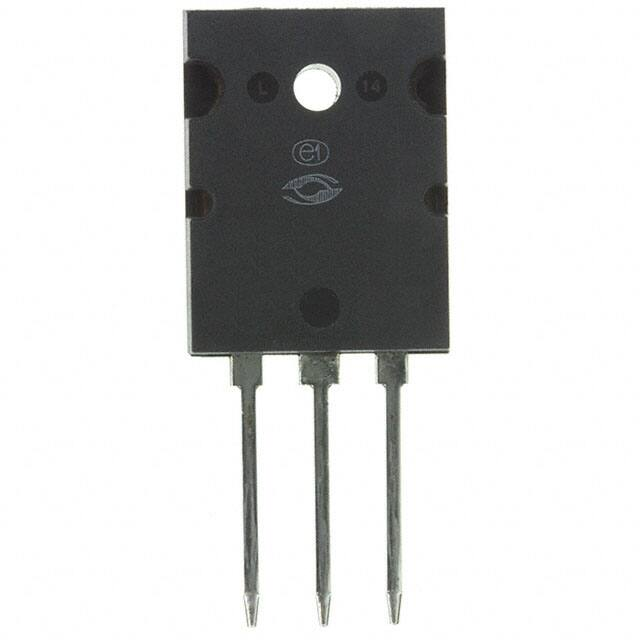
TO-264
Power Semiconductors
• Ultra low RDS(ON)
• Low Miller Capacitance
• Ultra Low Gate Charge, Qg
• Avalanche Energy Rated
• Popular T-MAX™ or TO-264 Package
D
G
S
Unless stated otherwise, Microsemi discrete MOSFETs contain a single MOSFET die. This device is made with
two parallel MOSFET die. It is intended for switch-mode operation. It is not suitable for linear mode operation.
MAXIMUM RATINGS
Symbol
All Ratings: TC = 25°C unless otherwise specified.
Parameter
APT34N80B2C3_LC3
UNIT
Drain-Source Voltage
800
Volts
ID
Continuous Drain Current @ TC = 25°C
34
IDM
Pulsed Drain Current
VGS
Gate-Source Voltage Continuous
±20
VGSM
Gate-Source Voltage Transient
±30
Total Power Dissipation @ TC = 25°C
417
Watts
Linear Derating Factor
3.33
W/°C
VDSS
PD
TJ,TSTG
TL
dv/
dt
1
Amps
102
Volts
-55 to 150
Operating and Storage Junction Temperature Range
°C
Lead Temperature: 0.063" from Case for 10 Sec.
300
Drain-Source Voltage slope (VDS = 640V, ID = 34A, TJ = 125°C)
50
V/ns
Amps
IAR
Repetitive Avalanche Current
7
17
EAR
Repetitive Avalanche Energy
7
0.5
EAS
Single Pulse Avalanche Energy
4
mJ
670
STATIC ELECTRICAL CHARACTERISTICS
MIN
BVDSS
Drain-Source Breakdown Voltage (VGS = 0V, ID = 500µA)
800
RDS(on)
Drain-Source On-State Resistance
IDSS
IGSS
VGS(th)
2
(VGS = 10V, ID = 22A)
Zero Gate Voltage Drain Current (VDS = 800V, VGS = 0V)
TYP
0.125
0.145
1.0
50
500
Gate-Source Leakage Current (VGS = ±20V, VDS = 0V)
2.10
UNIT
Volts
Zero Gate Voltage Drain Current (VDS = 800V, VGS = 0V, TJ = 150°C)
Gate Threshold Voltage (VDS = VGS, ID = 2mA)
MAX
3
Ohms
µA
±200
nA
3.9
Volts
CAUTION: These Devices are Sensitive to Electrostatic Discharge. Proper Handling Procedures Should Be Followed.
Microsemi Website - http://www.microsemi.com
"COOLMOS™ comprise a new family of transistors developed by Infineon Technologies AG. "COOLMOS" is a trademark of Infineon Technologies AG"
6-2006
Characteristic / Test Conditions
050-7147 Rev F
Symbol
�DYNAMIC CHARACTERISTICS
Symbol
APT34N80B2C3 _LC3
Test Conditions
Characteristic
MIN
TYP
C iss
Input Capacitance
Coss
Output Capacitance
VDS = 25V
2050
C rss
Reverse Transfer Capacitance
f = 1 MHz
110
VGS = 10V
180
VDD = 400V
22
Qg
Total Gate Charge
Qgs
Gate-Source Charge
Qgd
Gate-Drain ("Miller ") Charge
td(on)
Turn-on Delay Time
tr
ID = 34A @ 25°C
tf
RG = 2.5Ω
Eon
Turn-on Switching Energy
Eoff
Turn-off Switching Energy
Eon
Turn-on Switching Energy
Eoff
Turn-off Switching Energy
INDUCTIVE SWITCHING @ 25°C
6
70
80
6
9
ns
675
VDD = 533V, VGS = 15V
6
nC
15
VDD = 400V
ID = 34A @ 125°C
Fall Time
355
25
VGS = 10V
Turn-off Delay Time
pF
90
RESISTIVE SWITCHING
Rise Time
td(off)
UNIT
4510
VGS = 0V
3
MAX
ID = 34A, RG = 5Ω
580
INDUCTIVE SWITCHING @ 125°C
1145
VDD = 533V, VGS = 15V
ID = 34A, RG = 5Ω
µJ
670
SOURCE-DRAIN DIODE RATINGS AND CHARACTERISTICS
Symbol
MIN
Characteristic / Test Conditions
TYP
MAX
34
UNIT
IS
Continuous Source Current (Body Diode)
ISM
Pulsed Source Current
1
VSD
Diode Forward Voltage
2
t rr
Reverse Recovery Time (IS = -34A, dl S /dt = 100A/µs, VR = 400V)
855
ns
Q rr
Reverse Recovery Charge (IS = -34A, dl S /dt = 100A/µs, VR = 400V)
30
µC
dv/
Peak Diode Recovery
dt
dv/
102
(Body Diode)
1
(VGS = 0V, IS = -34A)
dt
1.2
Amps
Volts
6
V/ns
MAX
UNIT
5
THERMAL CHARACTERISTICS
Symbol
Characteristic
MIN
TYP
RθJC
Junction to Case
.30
RθJA
Junction to Ambient
40
1 Repetitive Rating: Pulse width limited by maximum junction
temperature
2 Pulse Test: Pulse width < 380 µs, Duty Cycle < 2%
3 See MIL-STD-750 Method 3471
4 Starting Tj = +25°C, L = 115.92mH, RG = 25Ω, Peak IL = 3.4A
5 IS = -34A di/dt = 100A/µs VR = 480V TJ = 125°C
6 Eon includes diode reverse recovery. See figures 18, 20.
7 Repetitve avalanche causes additional power losses that can be
calculated as PAV=EAR*f
Microsemi reserves the right to change, without notice, the specifications and information contained herein.
0.30
0.9
0.25
0.7
0.20
0.5
Note:
0.10
0.3
0.05
0.1
0
PDM
Z JC, THERMAL IMPEDANCE (°C/W)
θ
050-7147 Rev F
6-2006
0.35
0.15
t1
t2
SINGLE PULSE
0.05
10-5
10-4
°C/W
Duty Factor D = t1/t2
Peak TJ = PDM x ZθJC + TC
10-3
10-2
10-1
RECTANGULAR PULSE DURATION (SECONDS)
FIGURE 1, MAXIMUM EFFECTIVE TRANSIENT THERMAL IMPEDANCE, JUNCTION-TO-CASE vs PULSE DURATION
1.0
�Typical Performance Curves
TC ( C)
0.183
ZEXT
0.117
Dissipated Power
(Watts)
0.00828
0.174
ZEXT are the external thermal
impedances: Case to sink,
sink to ambient, etc. Set to
zero when modeling only
the case to junction.
ID, DRAIN CURRENT (AMPERES)
TJ ( C)
VDS> ID (ON) x RDS (ON)MAX.
250 µSEC. PULSE TEST
@
很抱歉,暂时无法提供与“APT34N80LC3G”相匹配的价格&库存,您可以联系我们找货
免费人工找货