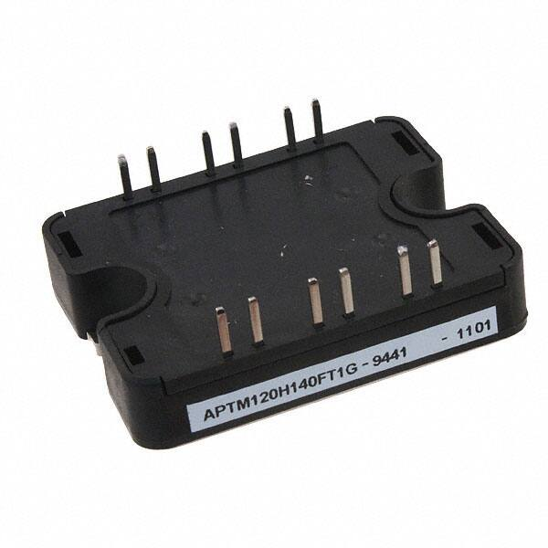
APTM120H140FT1G
VDSS = 1200V
RDSon = 1.4 typ @ Tj = 25°C
ID = 8A @ Tc = 25°C
Full - Bridge
MOSFET Power Module
4
3
Q1
Q3
5
6
2
1
Q2
Q4
7
9
8
11
10
NTC
12
Application
Welding converters
Switched Mode Power Supplies
Uninterruptible Power Supplies
Motor control
Features
Power MOS 8™ Fast FREDFETs
- Low RDSon
- Low input and Miller capacitance
- Low gate charge
- Fast intrinsic reverse diode
- Avalanche energy rated
- Very rugged
Very low stray inductance
- Symmetrical design
Internal thermistor for temperature monitoring
High level of integration
Benefits
Pins 3/4 must be shorted together
Outstanding performance at high frequency operation
Direct mounting to heatsink (isolated package)
Low junction to case thermal resistance
Solderable terminals both for power and signal for
easy PCB mounting
Low profile
Each leg can be easily paralleled to achieve a phase
leg of twice the current capability
RoHS Compliant
Absolute maximum ratings
ID
IDM
VGS
RDSon
PD
IAR
Parameter
Drain - Source Breakdown Voltage
Tc = 25°C
Tc = 80°C
Continuous Drain Current
Pulsed Drain current
Gate - Source Voltage
Drain - Source ON Resistance
Maximum Power Dissipation
Avalanche current (repetitive and non repetitive)
Tc = 25°C
Max ratings
1200
8
6
50
±30
1.68
208
7
Unit
V
A
V
W
A
These Devices are sensitive to Electrostatic Discharge. Proper Handling Procedures Should Be Followed. See application note
APT0502 on www.microsemi.com
www.microsemi.com
1–7
APTM120H140FT1G – Rev 1 October, 2012
Symbol
VDSS
�APTM120H140FT1G
All ratings @ Tj = 25°C unless otherwise specified
Electrical Characteristics
Symbol Characteristic
IDSS
RDS(on)
VGS(th)
IGSS
Zero Gate Voltage Drain Current
Drain – Source on Resistance
Gate Threshold Voltage
Gate – Source Leakage Current
Test Conditions
Tj = 25°C
VDS = 1200V
VGS = 0V
Tj = 125°C
VGS = 10V, ID = 7A
VGS = VDS, ID = 1mA
VGS = ±30 V
Min
3
Typ
1.4
4
Max
250
1000
1.68
5
±100
Unit
Max
Unit
µA
V
nA
Dynamic Characteristics
Symbol
Ciss
Coss
Crss
Characteristic
Input Capacitance
Output Capacitance
Reverse Transfer Capacitance
Qg
Total gate Charge
Qgs
Gate – Source Charge
Qgd
Gate – Drain Charge
Td(on)
Turn-on Delay Time
Tr
Td(off)
Tf
Rise Time
Turn-off Delay Time
Fall Time
Test Conditions
VGS = 0V
VDS = 25V
f = 1MHz
Min
Typ
3812
350
44
pF
145
VGS = 10V
VBus = 600V
ID = 7A
nC
24
70
26
Resistive switching @ 25°C
VGS = 15V
VBus = 800V
ID = 7A
RG = 4.7
15
ns
85
24
Source - Drain diode ratings and characteristics
Symbol Characteristic
IS
Continuous Source current
(Body diode)
VSD
Diode Forward Voltage
dv/dt Peak Diode Recovery
trr
Reverse Recovery Time
Qrr
Reverse Recovery Charge
Test Conditions
Min
Typ
Tj = 25°C
Max
8
6
1
25
250
Tj = 125°C
520
Tc = 25°C
Tc = 80°C
VGS = 0V, IS = - 7A
IS = - 7A
VR = 100V
diS/dt = 100A/µs
Tj = 25°C
1.12
Tj = 125°C
3.03
Unit
A
V
V/ns
ns
µC
www.microsemi.com
2–7
APTM120H140FT1G – Rev 1 October, 2012
dv/dt numbers reflect the limitations of the circuit rather than the device itself.
IS - 7A di/dt 1000A/µs
VDD 800V
Tj 125°C
�APTM120H140FT1G
Thermal and package characteristics
Symbol
RthJC
VISOL
TJ
TSTG
TC
Torque
Wt
Characteristic
Junction to Case Thermal Resistance
Min
RMS Isolation Voltage, any terminal to case t =1 min, 50/60Hz
4000
-40
-40
-40
2
Operating junction temperature range
Storage Temperature Range
Operating Case Temperature
Mounting torque
Package Weight
To heatsink
M4
Typ
Max
0.6
150
125
100
3
80
Unit
°C/W
V
°C
N.m
g
Temperature sensor NTC (see application note APT0406 on www.microsemi.com for more information).
Symbol Characteristic
R25
Resistance @ 25°C
B 25/85 T25 = 298.15 K
RT
Min
Typ
50
3952
Max
Unit
k
K
R25
T: Thermistor temperature
1
1 RT: Thermistor value at T
exp B25 / 85
T25 T
See application note 1904 - Mounting Instructions for SP1 Power Modules on www.microsemi.com
www.microsemi.com
3–7
APTM120H140FT1G – Rev 1 October, 2012
SP1 Package outline (dimensions in mm)
�APTM120H140FT1G
Typical Performance Curve
Low Voltage Output Characteristics
Low Voltage Output Characteristics
20
12
ID, Drain Current (A)
TJ=25°C
15
10
TJ=125°C
5
0
TJ=125°C
VGS=6, 7, 8 &9V
10
8
5V
6
4
4.5V
2
0
0
5
10
15
20
0
5
10
3
VGS=10V
ID=7A
20
25
30
2
1.5
1
0.5
0
VDS > ID(on)xRDS(on)MAX
250µs pulse test @ < 0.5 duty cycle
8
6
TJ=125°C
4
TJ=25°C
2
0
25
50
75
100
125
150
0
1
2
3
4
5
Capacitance vs Drain to Source Voltage
Gate Charge vs Gate to Source
10000
12
C, Capacitance (pF)
10
Ciss
VDS=240V
ID=7A
TJ=25°C
VDS=600V
8
VDS=960V
6
6
VGS, Gate to Source Voltage (V)
TJ, Junction Temperature (°C)
VGS, Gate to Source Voltage
15
Transfert Characteristics
Normalized RDS(on) vs. Temperature
2.5
10
VDS, Drain to Source Voltage (V)
ID, Drain Current (A)
RDSon, Drain to Source ON resistance
VDS, Drain to Source Voltage (V)
4
2
1000
Coss
100
Crss
10
0
0
40
80
120
160
Gate Charge (nC)
0
50
100
150
200
VDS, Drain to Source Voltage (V)
www.microsemi.com
4–7
APTM120H140FT1G – Rev 1 October, 2012
ID, Drain Current (A)
VGS=10V
�APTM120H140FT1G
ISD, Reverse Drain Current (A)
Drain Current vs Source to Drain Voltage
25
20
TJ=125°C
15
10
5
TJ=25°C
0
0
0.2
0.4
0.6
0.8
1
VSD, Source to Drain Voltage (V)
Maximum Effective Transient Thermal Impedance, Junction to Case vs Pulse Duration
0.6
0.5
0.4
0.3
0.9
0.7
0.5
0.2
0.3
0.1
0.1
0.05
0
0.00001
Single Pulse
0.0001
0.001
0.01
0.1
1
10
rectangular Pulse Duration (Seconds)
www.microsemi.com
5–7
APTM120H140FT1G – Rev 1 October, 2012
Thermal Impedance (°C/W)
0.7
�APTM120H140FT1G
DISCLAIMER
The information contained in the document (unless it is publicly available on the Web without access restrictions) is
PROPRIETARY AND CONFIDENTIAL information of Microsemi and cannot be copied, published, uploaded, posted,
transmitted, distributed or disclosed or used without the express duly signed written consent of Microsemi. If the
recipient of this document has entered into a disclosure agreement with Microsemi, then the terms of such Agreement
will also apply. This document and the information contained herein may not be modified, by any person other than
authorized personnel of Microsemi. No license under any patent, copyright, trade secret or other intellectual property
right is granted to or conferred upon you by disclosure or delivery of the information, either expressly, by implication,
inducement, estoppels or otherwise. Any license under such intellectual property rights must be approved by
Microsemi in writing signed by an officer of Microsemi.
Microsemi reserves the right to change the configuration, functionality and performance of its products at anytime
without any notice. This product has been subject to limited testing and should not be used in conjunction with lifesupport or other mission-critical equipment or applications. Microsemi assumes no liability whatsoever, and Microsemi
disclaims any express or implied warranty, relating to sale and/or use of Microsemi products including liability or
warranties relating to fitness for a particular purpose, merchantability, or infringement of any patent, copyright or other
intellectual property right. Any performance specifications believed to be reliable but are not verified and customer or
user must conduct and complete all performance and other testing of this product as well as any user or customers final
application. User or customer shall not rely on any data and performance specifications or parameters provided by
Microsemi. It is the customer’s and user’s responsibility to independently determine suitability of any Microsemi
product and to test and verify the same. The information contained herein is provided “AS IS, WHERE IS” and with all
faults, and the entire risk associated with such information is entirely with the User. Microsemi specifically disclaims
any liability of any kind including for consequential, incidental and punitive damages as well as lost profit. The product
is subject to other terms and conditions which can be located on the web at http://www.microsemi.com/legal/tnc.asp
Life Support Application
Seller's Products are not designed, intended, or authorized for use as components in systems intended for space,
aviation, surgical implant into the body, in other applications intended to support or sustain life, or for any other
application in which the failure of the Seller's Product could create a situation where personal injury, death or property
damage or loss may occur (collectively "Life Support Applications").
Buyer agrees not to use Products in any Life Support Applications and to the extent it does it shall conduct extensive
testing of the Product in such applications and further agrees to indemnify and hold Seller, and its officers, employees,
subsidiaries, affiliates, agents, sales representatives and distributors harmless against all claims, costs, damages and
expenses, and attorneys' fees and costs arising, directly or directly, out of any claims of personal injury, death, damage
or otherwise associated with the use of the goods in Life Support Applications, even if such claim includes allegations
that Seller was negligent regarding the design or manufacture of the goods.
www.microsemi.com
6–7
APTM120H140FT1G – Rev 1 October, 2012
Buyer must notify Seller in writing before using Seller’s Products in Life Support Applications. Seller will study with
Buyer alternative solutions to meet Buyer application specification based on Sellers sales conditions applicable for the
new proposed specific part.
�Mouser Electronics
Authorized Distributor
Click to View Pricing, Inventory, Delivery & Lifecycle Information:
Microsemi:
APTM120H140FT1G
�