AT17F040A and AT17F080A
FPGA Configuration Flash Memory
DATASHEET
Features
Programmable 4,194,304 x 1 and 8,388,608 x 1-bit Serial Memories Designed
to Store Configuration Programs for Field Programmable Gate Arrays (FPGAs)
3.3V Output Capability
5.0V Tolerant I/O Pins
Program Support using the Atmel ATDH2200E System, ATDH2225 ISP cable,
or Third-party Programmers
In-System Programmable (ISP) via 2-wire Bus
Simple Interface to SRAM FPGAs
Compatible with Atmel AT40K and AT94K Devices, Altera® FLEX®, Excalibur™,
Stratix®, Cyclone™, and APEX™ Devices
Cascadable Read-back to Support Additional Configurations or Higher-density
Arrays
Low-power CMOS FLASH Process
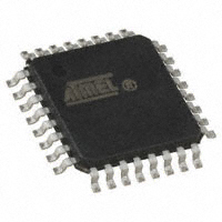
Available in 8-pad LAP and 20-lead PLCC Packages
Emulation of the Atmel AT24C Serial EEPROMs
Low-power Standby Mode
Single Device Capable of Holding 4-Bitstream Files Allowing Simple System
Reconfiguration
Fast Serial Download Speeds up to 33MHz
Endurance: 100,000 Write Cycles Typical
Green (Lead/Halide-free/ROHS compliant) Package Options
Description
The Atmel® AT17FxxxA Series of In-System Programmable Configuration
PROMs (Configurators) provide an easy-to-use, cost-effective configuration
memory solution for FPGAs. The AT17FxxxA Series devices are packaged in the
8-pad LAP and 20-lead PLCC (Table 1-1). The AT17FxxxA Series Configurators
use a simple serial-access procedure to configure one or more FPGA devices.
The AT17FxxxA Series Configurators can be programmed with industry-standard
programmers, the Atmel ATDH2200E Programming Kit or the Atmel ATDH2225
ISP Cable.
Table 1.
AT17FxxxA Series Packages
Package
AT17F040A
AT17F080A
8-pad LAP
Yes
Yes
20-lead PLCC
Yes
Yes
Atmel-2823E-CNFG-AT17F040A-080A-Datasheet_012015
�1.
Pin Configurations
Table 1-1.
Pin
Description
DATA(1)
Three-state DATA output for FPGA Configuration. Open-collector bi-directional pin for
configuration programming.
DCLK(1)
Three-state Clock. Functions as an input when the Configurator is in programming mode (i.e.
SER_EN is Low) and as an output during FPGA configuration.
PAGE_EN(2)
Enable Page Download Mode Input. When PAGE_EN is high the configuration download address
space is partitioned into four equal pages. This gives users the ability to easily store and retrieve
multiple configuration bitstreams from a single configuration device. This input works in conjunction
with the PAGESEL inputs. PAGE_EN must be remain low if paging is not desired. When SER_EN is
Low (ISP mode) this pin has no effect.
PAGESEL[1:0](2)
Page Select Inputs. Used to determine which of the four memory pages are targeted during a serial
configuration download. The address space for each of the pages is shown in Table 1-2. When
SER_EN is Low (ISP mode) these pins have no effect.
RESET/OE(1)
Output Enable (Active High) and RESET (Active Low) when SER_EN is High. A Low level on
RESET/OE resets both the address and bit counters. A High level (with nCS Low) enables the data
output driver.
nCS
Chip Enable Input (Active Low). A Low level (with OE High) allows DCLK to increment the address
counter and enables the data output driver. A High level on nCS disables both the address and bit
counters and forces the device into a low-power standby mode. Note that this pin will not
enable/disable the device in the 2-wire Serial Programming mode (SER_EN Low).
GND
Ground. A 0.2μF decoupling capacitor between VCC and GND is recommended.
nCASC
Cascade Select Output (when SER_EN is High). This output goes Low when the internal address
counter has reached its maximum value. If the PAGE_EN input is set High, the maximum value is the
highest address in the selected partition. The PAGESEL[1:0] inputs are used to make the four
partition selections. If the PAGE_EN input is set Low, the device is not partitioned and the address
maximum value is the highest address in the device (Table 1-2). In a daisy chain of the AT17FxxxA
Series devices, the nCASC pin of one device must be connected to the nCS input of the next device
in the chain. It will stay Low as long as nCS is Low and OE is High. It will then follow nCS until OE
goes Low; thereafter, nCASC will stay High until the entire EEPROM is read again.
A2(1)
Device Selection Input, (when SER_EN Low). The input is used to enable (or chip select) the
device during programming (i.e., when SER_EN is Low). Refer to the Atmel AT17FxxxA
Programming Specification available at www.atmel.com for additional details.
READY
Open Collector Reset State Indicator. Driven Low during power-up reset, released when power-up
is complete. (recommended 4.7k pull-up on this pin if used).
SER_EN(1)
Serial Enable Input. Must remain High during FPGA configuration operations. Bringing SER_EN
Low enables the 2-Wire Serial Programming Mode. For non-ISP applications, SER_EN should be
tied to VCC.
VCC
Device Power Supply. +3.3V (±10%)
(1)
Notes:
2
Pin Descriptions
1.
2.
Internal 20K pull-up resistor
Internal 30K pull-up resistor
AT17F040A/080A [DATASHEET]
Atmel-2823E-CNFG-AT17F040A-080A-Datasheet_012015
�Table 1-2.
Address Space (PAGESEL[1:0])
Paging Decodes
AT17F040A (4Mb)
AT17F080A (8Mb)
PAGESEL = 00, PAGE_EN = 1
00000 – 0FFFFh
00000 – 1FFFFh
PAGESEL = 01, PAGE_EN = 1
10000 – 1FFFFh
20000 – 3FFFFh
PAGESEL = 10, PAGE_EN = 1
20000 – 2FFFFh
40000 – 5FFFFh
PAGESEL = 11, PAGE_EN = 1
30000 – 3FFFFh
60000 – 7FFFFh
PAGESEL = XX, PAGE_EN = 0
00000 – 3FFFFh
00000 – 7FFFFh
Table 1-3.
Pin Configurations
Name
I/O
8-pad LAP
20-lead PLCC
DATA
I/O
1
2
DCLK
I
2
4
PAGE_EN
I
—
16
PAGESEL0
I
—
11
PAGESEL1
I
—
7
RESET/OE
I
3
8
nCS
I
4
9
GND
–
5
10
nCASC
O
6
12
A2
I
6
12
READY
O
—
15
SER_EN
I
7
18
VCC
–
8
20
Figure 1-1.
Pinouts
NC
VCC
NC
20
19
SER_EN
17
NC
NC
6
16
PAGE_EN
PAGESEL1
7
15
READY
RESET/OE
8
14
NC
13
18
5
NC
Drawings are not to scale.
4
NC
12
Note:
DCLK
(A2) nCASC
GND
DATA
(A2) nCASC
5
1
6
4
11
3
nCS
PAGESEL0
RESET/OE
10
SER_EN
9
7
1
nCS
VCC
2
DATA
GND
8
DCLK
NC
(Top View)
2
20-lead PLCC
(Top View)
3
8-pad LAP
AT17F040A/080A [DATASHEET]
Atmel-2823E-CNFG-AT17F040A-080A-Datasheet_012015
3
�2.
Block Diagram
Figure 2-1.
READY
PAGE_EN
PAGESEL0
PAGESEL1
Block Diagram
Power-on
Reset
Reset
Clock/Oscillator
Logic
nCASC(A2)
Configuration
Page Select
Serial Download Logic
2-wire Serial Programming
Flash
Memory
DCLK
CE/WE/OE
Data
Address
DATA
nCS
Control Logic
RESET/OE
SER_EN
4
AT17F040A/080A [DATASHEET]
Atmel-2823E-CNFG-AT17F040A-080A-Datasheet_012015
�3.
Device Description
The control signals for the configuration memory device (nCS, RESET/OE and DCLK) interface directly with the
FPGA device control signals. All FPGA devices can control the entire configuration process and retrieve data
from the configuration device without requiring an external intelligent controller.
The RESET/OE and nCS pins control the tri-state buffer on the DATA output pin and enable the address
counter. When RESET/OE is driven Low, the configuration device resets its address counter and tri-states its
DATA pin. The nCS pin also controls the output of the AT17FxxxA Series Configurator. If nCS is held High after
the RESET/OE reset pulse, the counter is disabled and the DATA output pin is tri-stated. When OE is
subsequently driven High, the counter and the DATA output pin are enabled. When RESET/OE is driven Low
again, the address counter is reset and the DATA output pin is tri-stated, regardless of the state of nCS.
When the configurator has driven out all of its data and nCASC is driven Low, the device tri-states the DATA pin
to avoid contention with other configurators. Upon power-up, the address counter is automatically reset.
4.
FPGA Master Serial Mode Summary
The I/O and logic functions of any SRAM-based FPGA are established by a configuration program. The
program is loaded either automatically upon power-up or on command, depending on the state of the FPGA
mode pins. In Master mode, the FPGA automatically loads the configuration program from an external memory.
The AT17FxxxA Serial Configuration PROM has been designed for compatibility with the Master Serial mode.
This document discusses the Atmel AT40K, AT40KAL and AT94KAL applications as well as Altera applications.
5.
Control of Configuration
Most connections between the FPGA device and the AT17FxxxA Serial Configurator PROM are simple and
self-explanatory.
6.
The DATA output of the AT17FxxxA Series Configurator drives DIN of the FPGA devices.
The DCLK output of the AT17FxxxA drives the DCLK input data of the FPGA.
The nCASC output of a AT17FxxxA Series Configurator drives the nCS input of the next Configurator in a
cascade chain of configurator devices.
SER_EN must be at logic High level (internal pull-up resistor provided) except during ISP.
The READY pin is available as an open-collector indicator of the device’s reset status; it is driven Low
while the device is in its power-on reset cycle and released (tri-stated) when the cycle is complete.
PAGE_EN must REMAIN Low if download paging is not desired. If paging is desired, PAGE_EN must be
High and the PAGESEL pins must be set to High or Low such that the desired page is selected
(Table 1-2).
Cascading Serial Configuration Devices
For multiple FPGAs configured as a daisy-chain or for FPGAs requiring larger configuration memories,
cascaded configurators provide additional memory.
After the last bit from the first configurator is read, the clock signal to the configurator asserts its nCASC output
Low and disables its DATA line driver. The second configurator recognizes the Low level on its nCS input and
enables its DATA output.
After configuration is complete, the address counters of all cascaded configurators are reset if the RESET/OE
on each configurator is driven to its active (Low) level.
If the address counters are not to be reset upon completion, then the RESET/OE input can be tied to its inactive
(High) level.
AT17F040A/080A [DATASHEET]
Atmel-2823E-CNFG-AT17F040A-080A-Datasheet_012015
5
�7.
Programming Mode
The programming mode is entered by bringing SER_EN Low. In this mode, the chip can be programmed by the
2-wire serial bus. The programming is done at VCC supply only. Programming super voltages are generated
inside the chip. The AT17FxxxA parts are read/write at 3.3V nominal. Refer to the Atmel AT17FxxxA
Programming Specification available at www.atmel.com for more programming details. The AT17FxxxA devices
are supported by the ATDH2200 programming system along with many third party programmers.
8.
Standby Mode
The AT17FxxxA Series Configurators enter a low-power standby mode whenever SER_EN is High and nCS is
asserted High. In this mode, the AT17FxxxA Configurator typically consumes less than 3mA of current at 3.3V.
The output remains in a high-impedance state regardless of the state of the OE input.
6
AT17F040A/080A [DATASHEET]
Atmel-2823E-CNFG-AT17F040A-080A-Datasheet_012015
�9.
Electrical Specifications
9.1
Absolute Maximum Ratings*
Operating Temperature . . . . . . . . . . . . . . . . . . . -40C to +85C
Storage Temperature . . . . . . . . . . . . . . . . . . . . -65C to +150C
Voltage on Any Pin
with Respect to Ground . . . . . . . . . . . . . . . . .-0.5V to VCC +0.5V
Supply Voltage (VCC) . . . . . . . . . . . . . . . . . . . . . . -0.5V to +4.0V
Maximum Soldering Temp. (10 sec. @ 1/16in.) . . . . . . . . .260C
ESD (RZAP = 1.5K, CZAP = 100pF) . . . . . . . . . . . . . . . . . . 2000V
9.2
Operating Conditions
Table 9-1.
9.3
*Notice: Stresses beyond those listed under
Absolute Maximum Ratings may cause
permanent damage to the device. This is a
stress rating only and functional operation
of the device at these or any other
conditions beyond those listed under
operating conditions is not implied.
Exposure to Absolute Maximum Rating
conditions for extended periods of time
may affect device reliability.
Operating Conditions
Symbol
Description
Min
Max
Units
VCC
Supply voltage relative to GND -40C to +85C
2.97
3.63
V
DC Characteristics
Table 9-2.
DC Characteristics
AT17F040A
AT17F080A
Symbol
Description
Min
Max
Min
Max
Units
VIH
High-level Input Voltage
2.0
VCC
2.0
VCC
V
VIL
Low-level Input Voltage
0
0.8
0
0.8
V
VOH
High-level Output Voltage (IOH = -2mA)
VOL
Low-level Output Voltage (IOL = +3mA)
0.4
0.4
V
ICCA
Supply Current, Active Mode at Freq. Max.
50
50
mA
IL
Input or Output Leakage Current (VIN = VCC or GND)
10
μA
ICCS
Supply Current, Standby Mode
3
mA
2.4
-10
2.4
10
3
-10
V
AT17F040A/080A [DATASHEET]
Atmel-2823E-CNFG-AT17F040A-080A-Datasheet_012015
7
�9.4
AC Characteristics
Table 9-3.
AC Characteristics
AT17F040A/080A
Symbol
Description
TOE(1)
Max
Units
OE to Data Delay
55
ns
TCE(1)
nCS to Data Delay
60
ns
TCAC(1)
DCLK to Data Delay
30
ns
TOH
Data Hold from nCS, OE, or DCLK
TDF(2)
nCS or OE to Data Float Delay
TLC
DCLK Low Time
15
ns
THC
DCLK High Time
15
ns
TSCE
nCS Setup Time to DCLK
(to guarantee proper counting)
25
ns
THCE
nCS Hold Time from DCLK
(to guarantee proper counting)
0
ns
THOE
RESET/OE Low Time
(guarantees counter is reset)
20
ns
FMAX
Maximum Input Clock Frequency SEREN = 0
TWR
Write Cycle Time(3)
TEC
Notes:
Erase Cycle Time
1.
2.
3.
Table 9-4.
Min
Typ
0
ns
15
10
(3)
8
12
μs
33
s
AC Characteristics When Cascading
Symbol
Description
TCDF(2)
DCLK to Data Float Delay
TOCK(1)
TOCE(1)
TOOE(1)
1.
2.
MHz
AC test load = 50pF
Float delays are measured with 5pF AC loads. Transition is measured ± 200mV from steady-state
active levels.
Reference the Atmel AT17FxxxA Programming Specification for procedural information.
AT17F040A
Notes:
ns
Min
Max
AT17F080A
Min
Max
Units
50
50
ns
DCLK to nCASC Delay
55
55
ns
nCS to nCASC Delay
40
40
ns
RESET/OE to nCASC Delay
25
35
ns
AC test load = 50pF
Float delays are measured with 5pF AC loads. Transition is measured ± 200mV from steady-state active
levels.
AT17F040A/080A [DATASHEET]
Atmel-2823E-CNFG-AT17F040A-080A-Datasheet_012015
�Figure 9-1.
AC Waveforms
nCS
TSCE
TSCE
THCE
RESET/OE
TLC
THOE
THC
CLK
TOE
TOH
TCAC
TDF
TCE
DATA
TOH
Figure 9-2.
AC Waveforms when Cascading
RESET/OE
nCS
CLK
TCDF
DATA
FIRST BIT
LAST BIT
TOCK
TOCE
TOOE
nCASL
TOCE
AT17F040A/080A [DATASHEET]
Atmel-2823E-CNFG-AT17F040A-080A-Datasheet_012015
9
�10.
Ordering Information
10.1
Ordering Code Detail
AT 1 7 F 0 4 0 A - 3 0 C U
Package Device Grade
Atmel Designator
U = Green, Sn Lead Finish
Industrial Temperature Range
(-40°C to +85°C)
Product Family
17F = FPGA Flash
Configuration Memory
Package Option
Device Density
C = 8-pad LAP
J = 20-lead PLCC
040 = 4 megabit
080 = 8 megabit
Product Variation
30 = Default Value
Special Pinouts
A = Altera
Blank = Xilinx/Atmel/Other
10.2
Ordering Information
Memory Size
4-Mbit
8-Mbit
Atmel Ordering Code
AT17F040A-30CU
AT17F040A-30JU
AT17F080A-30CU
AT17F080A-30JU
Lead Finish
Package
Sn
(Lead-free/Halogen-free)
8CN4
Sn
(Lead-free/Halogen-free)
8CN4
20J
20J
Package Type
10
8CN4
8-pad, 6.00mm x 6.00mm x 1.04mm, Leadless Array Package (LAP)
Pin-compatible with 8-lead SOIC/VOIC Packages
20J
20-lead, Plastic J-leaded Chip Carrier (PLCC)
AT17F040A/080A [DATASHEET]
Atmel-2823E-CNFG-AT17F040A-080A-Datasheet_012015
Voltage
Operation Range
3.3V
Industrial
(-40C to 85C
3.3V
Industrial
(-40C to 85C
�11.
Packaging Information
11.1
8CN4 — 8-pad LAP
Marked Pin1 Indentifier
E
A
A1
D
Side View
Top View
Pin1 Corner
L1
0.10 mm
TYP
8
1
e
7
2
COMMON DIMENSIONS
(Unit of Measure = mm)
3
6
b
5
4
e1
L
Bottom View
Note:
1. Metal Pad Dimensions.
2. All exposed metal area shall have the following finished platings.
Ni: 0.0005 to 0.015 mm
Au: 0.0005 to 0.001 mm
SYMBOL
MIN
TYP
MAX
A
0.94
1.04
1.14
A1
0.30
0.34
0.38
D
5.89
5.99
6.09
E
5.89
5.99
6.09
e
1.27 BSC
e1
1.10 REF
NOTE
L
0.95
1.00
1.05
1
L1
1.25
1.30
1.35
1
b
0.45
0.50
0.55
1
12/22/14
Package Drawing Contact:
packagedrawings@atmel.com
TITLE
8CN4, 8-pad 6x6x1.04mm Body, 1.27mm pitch
Leadless Array Package (LAP)
GPC
DRAWING NO.
REV.
DMH
8CN4
E
AT17F040A/080A [DATASHEET]
Atmel-2823E-CNFG-AT17F040A-080A-Datasheet_012015
11
�11.2
20J — 20-lead PLCC
PIN NO. 1
1.14(0.045) X 45°
1.14(0.045) X 45°
0.318(0.0125)
0.191(0.0075)
IDENTIFIER
e
E1
E
D2/E2
B1
B
A2
D1
A1
D
A
0.51(0.020)MAX
45° MAX (3X)
COMMON DIMENSIONS
(Unit of Measure = mm)
Notes: 1. This package conforms to JEDEC reference MS-018, Variation AA
2. Dimensions D1 and E1 do not include mold protrusion.
Allowable protrusion is .010"(0.254mm) per side. Dimension D1
and E1 include mold mismatch and are measured at the extreme
material condition at the upper or lower parting line.
3. Lead coplanarity is 0.004" (0.102mm) maximum
SYMBOL
MIN
NOM
MAX
A
4.191
–
4.572
A1
2.286
–
3.048
A2
0.508
–
–
D
9.779
–
10.033
D1
8.890
–
9.042
E
9.779
–
10.033
E1
8.890
–
9.042
D2/E2
7.366
–
8.382
B
0.660
–
0.813
B1
0.330
–
0.533
e
NOTE
Note 2
Note 2
1.270 TYP
10/04/01
Package Drawing Contact:
packagedrawings@atmel.com
12
AT17F040A/080A [DATASHEET]
Atmel-2823E-CNFG-AT17F040A-080A-Datasheet_012015
TITLE
20J, 20-lead, Plastic J-leaded Chip Carrier (PLCC)
DRAWING NO. REV.
20J
B
�12.
Revision History
Doc Rev
Date
Comments
Removed commercial and 32-lead TQFP package options.
2838F
01/2015
Updated the 8CN4 package outline drawing, template, Atmel logos, and disclaimer page.
Added an ordering code detail.
2823E
10/2010
Changed Endurance from 5,000 to 100,000
Changed Typ from 13 to 33 in AC Characteristics table
AT17F040A/080A [DATASHEET]
Atmel-2823E-CNFG-AT17F040A-080A-Datasheet_012015
13
�XXXXXX
Atmel Corporation
1600 Technology Drive, San Jose, CA 95110 USA
T: (+1)(408) 441.0311
F: (+1)(408) 436.4200
|
www.atmel.com
© 2015 Atmel Corporation. / Rev.: Atmel-2823E-CNFG-AT17F040A-080A-Datasheet_012015.
Atmel®, Atmel logo and combinations thereof, Enabling Unlimited Possibilities®, and others are registered trademarks or trademarks of Atmel Corporation in U.S. and
other countries. Other terms and product names may be trademarks of others.
DISCLAIMER: The information in this document is provided in connection with Atmel products. No license, express or implied, by estoppel or otherwise, to any intellectual property right
is granted by this document or in connection with the sale of Atmel products. EXCEPT AS SET FORTH IN THE ATMEL TERMS AND CONDITIONS OF SALES LOCATED ON THE
ATMEL WEBSITE, ATMEL ASSUMES NO LIABILITY WHATSOEVER AND DISCLAIMS ANY EXPRESS, IMPLIED OR STATUTORY WARRANTY RELATING TO ITS PRODUCTS
INCLUDING, BUT NOT LIMITED TO, THE IMPLIED WARRANTY OF MERCHANTABILITY, FITNESS FOR A PARTICULAR PURPOSE, OR NON-INFRINGEMENT. IN NO EVENT
SHALL ATMEL BE LIABLE FOR ANY DIRECT, INDIRECT, CONSEQUENTIAL, PUNITIVE, SPECIAL OR INCIDENTAL DAMAGES (INCLUDING, WITHOUT LIMITATION, DAMAGES
FOR LOSS AND PROFITS, BUSINESS INTERRUPTION, OR LOSS OF INFORMATION) ARISING OUT OF THE USE OR INABILITY TO USE THIS DOCUMENT, EVEN IF ATMEL HAS
BEEN ADVISED OF THE POSSIBILITY OF SUCH DAMAGES. Atmel makes no representations or warranties with respect to the accuracy or completeness of the contents of this
document and reserves the right to make changes to specifications and products descriptions at any time without notice. Atmel does not make any commitment to update the information
contained herein. Unless specifically provided otherwise, Atmel products are not suitable for, and shall not be used in, automotive applications. Atmel products are not intended,
authorized, or warranted for use as components in applications intended to support or sustain life.
SAFETY-CRITICAL, MILITARY, AND AUTOMOTIVE APPLICATIONS DISCLAIMER: Atmel products are not designed for and will not be used in connection with any applications where
the failure of such products would reasonably be expected to result in significant personal injury or death (“Safety-Critical Applications”) without an Atmel officer's specific written
consent. Safety-Critical Applications include, without limitation, life support devices and systems, equipment or systems for the operation of nuclear facilities and weapons systems.
Atmel products are not designed nor intended for use in military or aerospace applications or environments unless specifically designated by Atmel as military-grade. Atmel products are
not designed nor intended for use in automotive applications unless specifically designated by Atmel as automotive-grade.
�


 工商网监
湘ICP备2023018690号
工商网监
湘ICP备2023018690号
