Atmel AT42QT1244
24-key QMatrix FMEA IEC/EN/UL60730 Touch Sensor
PRELIMINARY DATASHEET
Features
Number of keys:
Up to 24
Technology:
Patented charge-transfer (transverse mode), with frequency hopping
Key outline sizes:
6 mm × 6 mm or larger (panel thickness dependent); different sizes and
shapes possible
Key spacings:
8 mm or wider, center to center (panel thickness dependent)
Electrode design:
Two-part electrode shapes (drive-receive); wide variety of possible layouts
Layers required:
One layer (with jumpers), two layers (no jumpers)
Electrode materials:
PCB, FPCB, silver or carbon on film, ITO on film
Panel materials:
Plastic, glass, composites, painted surfaces (low particle density metallic
paints possible)
Panel thickness:
Up to 50 mm glass, 20 mm plastic (key size dependent)
Key sensitivity:
Individually settable via simple commands over communication interface
Interface:
I2C slave mode (up to 400 kHz data transfer speed)
Debug output
Signal processing:
Self-calibration, auto drift compensation, noise filtering, Adjacent Key
Suppression® (AKS®) technology
FMEA compliant design features
IEC/EN/UL60730 compliant design features
UL approval
VDE compliance
For use in both class B and class C safety-critical products
Detects and Reports Key Failure
Power:
+3 V to 5 V
Package:
32-pin 7 × 7 mm TQFP RoHS compliant
32-pin 5 × 5 mm QFN RoHS compliant
9631EX–AT42–12/13
�Y2B
SMP
SDA
SCL
29 28 27 26 25
24
Y1B
2
23
Y0B
VSS
3
22
A0
VDD
4
21
VSS
VSS
5
20
VDD
VDD
6
19
A1
X6
7
18
VDD
X7
8
17
9 10 11 12 13 14 15 16
X5
X4
X3
X2
X1
QT1244
X0
CHANGE
32 31 30
S_SYNC/DBG_DATA
1
VREF
M_SYNC
DBG_CLK
1.2
RST
Pinout Configuration
Y0A
1.1
Y1A
Pinout and Schematic
Y2A
1.
Pin Descriptions
Table 1-1.
Pin Descriptions
Pin
Name
Type
1
M_SYNC
I
2
CHANGE
OD
3
VSS
4
If Unused, connect
To...
Comments
Mains Sync input
Vdd
State change notification, active low. Has internal
20 k – 50 k pull-up resistor
Leave open
P
Ground
–
VDD
P
Power
–
5
VSS
P
Ground
–
6
VDD
P
Power
–
7
X6
O
X matrix drive line
Leave open
8
X7
O
X matrix drive line
Leave open
QT1244 [PRELIMINARY DATASHEET]
9631EX–AT42–12/13
2
�Table 1-1.
Pin Descriptions (Continued)
If Unused, connect
To...
Pin
Name
Type
Comments
9
DBG_CLK
O
Debug clock
Leave open
10
VREF
I
Connect to Vss
–
11
S_SYNC/
DBG_DATA
O
Oscilloscope sync / Debug data
Leave open
12
X0
O
X matrix drive line
Leave open
13
X1
O
X matrix drive line
Leave open
14
X2
O
X matrix drive line
Leave open
15
X3
O
X matrix drive line
Leave open
16
X4
O
X matrix drive line
Leave open
17
X5
O
X matrix drive line
Leave open
18
VDD
P
Power
–
19
A1
I
I2C address 1, read after reset
–
20
VDD
P
Power
–
21
VSS
P
Ground
–
22
A0
I
I2C address 0, read after reset
–
23
Y0B
I/O
Y line connection
Leave open
24
Y1B
I/O
Y line connection
Leave open
25
Y2B
I/O
Y line connection
Leave open
26
SMP
O
Sample output
–
27
SDA
OD
Serial data line
–
28
SCL
OD
Serial clock line
–
29
RST
I
Reset low; has internal 30 k – 60 k pull-up
resistor. This pin should be controlled by the host.
Leave open or Vdd
30
Y0A
I/O
Y line connection
Leave open
31
Y1A
I/O
Y line connection
Leave open
32
Y2A
I/O
Y line connection
Leave open
I
Input only
O
Output only, push-pull
OD
Open-drain output
P
Ground or power
I/O
Input and output
QT1244 [PRELIMINARY DATASHEET]
9631EX–AT42–12/13
3
�1.3
Schematic
Figure 1-1. Typical Circuit
VDD
Vunreg
Follow regulator manufacturer's recommended values
for input and output bypass capacitors Creg.
Keep the output capacitor close to pins 4 and 6.
Add a 100 nF capacitor close to pin 18.
VREG
Creg
Creg
*Rx7
MATRIX X DRIVE
*Rx6
VDD
*Rx5
*Rx4
Rp1
Rp2
*Rx3
QT1244
*Rx2
I2C
*Rx1
SDA
*Rx0
SCL
CHANGE
* optional - for emission suppression
** optional - for RF susceptibility improvement
MAINS SYNC
SCOPE SYNC
Cs0
Cs1
**Ry1
**Ry2
MATRIX Y SCAN IN
**Ry0
Cs2
Rs2
Rs1
Rs0
Note:
1) It is important to place all Cs, Rs, Rx and Ry
components physically near to the chip.
2) Leave YnA, YnB unconnected if not used.
For component values in Figure 1-1 check the following sections:
Section 3.3 on page 6: Cs capacitors (Cs0 – Cs2)
Section 3.5 on page 8: Sample resistors (Rs0 – Rs2)
Section 3.7 on page 8: Matrix resistors (Rx0 – Rx7, Ry0 – Ry2)
Section 3.10 on page 11: Voltage levels
QT1244 [PRELIMINARY DATASHEET]
9631EX–AT42–12/13
4
�2.
Overview
The AT42QT1244 (QT1244) device is a digital burst mode charge-transfer (QT™) sensor, designed specifically for
matrix layout touch controls. It includes all signal processing functions necessary to provide stable sensing under a
wide variety of changing conditions. Only a few external parts are required for operation. The entire circuit can be
built within a few square centimeters of single-sided PCB area. CEM-1 and FR1 punched, single-sided materials can
be used for the lowest possible cost. The rear of the PCB can be mounted flush on the back of a glass or plastic
panel using a conventional adhesive, such as 3M VHB two-sided adhesive acrylic film.
The QT1244 employs transverse charge-transfer (QT) sensing, a technology that senses changes in electrical
charge forced across two electrode elements by a pulse edge (see Figure 3.).
Figure 2-1. Field Flow Between X and Y Elements
overlying panel
X element
Y element
CMOS
driver
The QT1244 allows a wide range of key sizes and shapes to be mixed together in a single touch panel (see Section
3.8 on page 10).
The device uses an I2C interface to allow key data to be extracted and to permit individual key parameter setup. This
interface uses a memory mapped structure, designed to minimize the amount of data traffic while maximizing the
amount of information conveyed.
In addition to normal operating and setup functions the device can also report back actual signal strengths.
QmBtn software for the PC can be used to program the operation of the device as well as read back key status and
signal levels in real time.
The device also includes a Debug output interface, which can be used to monitor many operating variables during
product development.
QT1244 [PRELIMINARY DATASHEET]
9631EX–AT42–12/13
5
�3.
Hardware and Functional
3.1
Matrix Scan Sequence
The circuit operates by scanning each key sequentially. The keys are numbered from 0 – 23. Key scanning begins
with location X = 0, Y = 0 (key 0). All keys on Y0 are scanned first, then Y1 and finishing with all keys on Y2.
For example, the sequence is:
X0Y0, X1Y0 to X7Y0
X0Y1, X1Y1 to X7Y1
X0Y2, X1Y2 to X7Y2
Table 3-1 shows the key numbering.
Table 3-1.
Key Numbers
X7
X6
X5
X4
X3
X2
X1
X0
Y0
7
6
5
4
3
2
1
0
Y1
15
14
13
12
11
10
9
8
Y2
23
22
21
20
19
18
17
16
Key
numbers
Each key is sampled in a burst of acquisition pulses whose length is determined by the setups parameter BL
(Section 7. on page 45). This can be set on a per-key basis. A burst is completed entirely before the next key is
sampled. At the end of each burst the resulting signal is converted to digital form and processed. The burst length
directly impacts key gain. Each key can have a unique burst length in order to allow tailoring of key sensitivity on a
key-by-key basis.
3.2
Burst Paring
Keys that are disabled by setting NDIL to zero (Section 6.2.1 on page 30) are eliminated from the scan sequence to
save scan time and thus power. As a consequence, the fewer keys that are used the faster the device can respond.
All calibration times are reduced when keys are disabled.
3.3
Cs Sample Capacitor Operation
Cs capacitors absorb charge from the key electrodes on the rising edge of each X pulse. On each falling edge of X,
the Y matrix line is clamped to ground to allow the electrode and wiring charges to neutralize in preparation for the
next pulse. With each X pulse charge accumulates on Cs causing a staircase increase in its differential voltage.
After the burst completes, the device clamps the Y line to ground causing the opposite terminal to go negative. The
charge on Cs is then measured using an external resistor to ramp the negative terminal upwards until a zero
crossing is achieved. The time required to zero cross becomes the measurement result.
The Cs capacitors should be connected as shown in Figure 1-1 on page 4. They should be NP0 (preferred), X7R
ceramics or PPS film. NPO offers the best stability. The value of these capacitors is not critical but 4.7 nF is
recommended for most cases. If the transverse capacitive coupling from X to Y is large enough the voltage on a Cs
capacitor can saturate, destroying gain. In such cases the burst length should be reduced and/or the Cs value
increased. See Section 3.4.
If a Y line is not used its corresponding Cs capacitor may be omitted and the pins left floating.
QT1244 [PRELIMINARY DATASHEET]
9631EX–AT42–12/13
6
�3.4
Sample Capacitor; Saturation Effects
Cs voltage saturation at a pin YnB is shown in Figure 3-1. Saturation begins to occur when the voltage at a YnB pin
becomes more negative than –0.25 V at the end of the burst. This nonlinearity is caused by excessive voltage
accumulation on Cs inducing conduction in the pin protection diodes. This badly saturated signal destroys key gain
and introduces a strong thermal coefficient which can cause phantom detection.
Figure 3-1. VCs – Nonlinear During Burst
(Burst too long, or Cs too small, or X-Y transcapacitance too large)
X Drive
YnB
The cause of this is either from the burst length being too long, the Cs value being too small, or the X-Y transfer
coupling being too large. Solutions include loosening up the key structure interleaving, greater separation of the X
and Y lines on the PCB, increasing Cs, and decreasing the burst length.
Increasing Cs makes the part slower, decreasing burst length makes it less sensitive. A better PCB layout and a
looser key structure (up to a point) have no negative effects.
Cs voltages should be observed on an oscilloscope with the matrix layer bonded to the panel material. If the Rs side
of any Cs ramps is more negative than –0.25 V during any burst (not counting overshoot spikes which are probe
artifacts), there is a potential saturation problem.
Figure 3-2 shows a defective waveform similar to that of Figure 3-1, but in this case the distortion is caused by
excessive stray capacitance coupling from the Y line to AC ground (for example, from running too near and too far
alongside a ground trace, ground plane, or other traces). The excess coupling causes the charge-transfer effect to
dissipate a significant portion of the received charge from a key into the stray capacitance.
Figure 3-2. VCs – Poor Gain, Nonlinear During Burst
(Excess capacitance from Y line to Gnd)
X Drive
YnB
This phenomenon is more subtle. It can be best detected by increasing BL to a high count and watching what the
waveform does as it descends towards and below –0.25 V. The waveform appears deceptively straight, but it slowly
starts to flatten even before the –0.25 V level is reached.
A correct waveform is shown in Figure 3-3. Note that the bottom edge of the bottom trace is substantially straight
(ignoring the downward spikes).
QT1244 [PRELIMINARY DATASHEET]
9631EX–AT42–12/13
7
�Figure 3-3. VCs – Correct
X Drive
YnB
Unlike other QT circuits, the Cs capacitor values on QT1244 have no effect on conversion gain. However, they do
affect conversion time.
Unused Y lines should be left open.
3.5
Sample Resistors
The sample resistors (Rs0 – Rs2) are used to perform single-slope ADC conversion of the acquired charge on each
Cs capacitor. These resistors directly control acquisition gain. Larger values of Rs proportionately increase signal
gain. For most applications Rs should be 1 M. Unused Y lines do not require an Rs resistor.
3.6
Signal Levels
Using Atmel QmBtn software it is easy to observe the absolute level of signal received by the sensor on each key.
The signal values should normally be in the range of 200 – 750 counts with properly designed key shapes (see the
Touch Sensors Design Guide, available on the Atmel website) and values of Rs. However, long adjacent runs of X
and Y lines can also artificially boost the signal values, and induce signal saturation: this is to be avoided. The X-toY coupling should come mostly from intra-key electrode coupling, not from stray X-to-Y trace coupling.
QmBtn software is available free of charge on the Atmel web site.
The signal swing from the smallest finger touch should preferably exceed 8 counts, with 12 being a reasonable
target. The signal threshold setting (NTHR) should be set to a value guaranteed to be less than the signal swing
caused by the smallest touch.
Increasing the burst length (BL) parameter increases the signal strengths as does increasing the sampling resistor
(Rs) values.
3.7
Matrix Series Resistors
The X and Y matrix scan lines can use series resistors (Rx0 – Rx7 and Ry0 – Ry2 respectively) for improved EMC
performance (Figure 1-1 on page 4).
X drive lines require Rx in most cases to reduce edge rates and thus reduce RF emissions. Values range from
1 k – 100 k, typically 1 k.
Y lines need Ry to reduce EMC susceptibility problems and in some extreme cases, ESD. Values range from 1 k –
100 k, typically 1 k.Y resistors act to reduce noise susceptibility problems by forming a natural low-pass filter with
the Cs capacitors.
It is essential that the Rx and Ry resistors and Cs capacitors be placed very close to the chip. Placing these parts
more than a few millimeters away opens the circuit up to high frequency interference problems (above 20 MHz) as
the trace lengths between the components and the chip start to act as RF antennae.
The upper limits of Rx and Ry are reached when the signal level and hence key sensitivity are clearly reduced. The
limits of Rx and Ry depend on key geometry and stray capacitance, and thus an oscilloscope is required to
determine optimum values of both.
QT1244 [PRELIMINARY DATASHEET]
9631EX–AT42–12/13
8
�Dwell time is the duration in which charge coupled from X to Y is captured. Increasing the dwell time recovers some
of the signal levels lost to higher values of Rx and Ry, as shown in Figure 3-4. Too short a dwell time causes charge
to be lost if there is too much rising edge roll-off. Lengthening the dwell time causes this lost charge to be recaptured,
thereby restoring key sensitivity. Dwell time is adjustable (see Section 6.10.1 on page 39) to one of 8 values.
Figure 3-4. Drive Pulse Roll-off and Dwell Time
X drive
Dwell time
Lost charge due to
inadequate settling
before end of dwell time
Y gate
Dwell time problems can also be solved by either reducing the stray capacitance on the X line(s) (by a layout
change, for example by reducing X line exposure to nearby ground planes or traces), or, the Rx resistor needs to be
reduced in value (or a combination of both approaches).
One way to determine X settling time is to monitor the fields using a patch of metal foil or a small coin over the key
(Figure 3-5). Only one key along a particular X line needs to be observed, as each of the keys along that X line will
be identical. The chosen dwell time should exceed the observed 95% settling of the X-pulse by 25% or more.
Figure 3-5. Probing X-Drive Waveforms With a Coin
QT1244 [PRELIMINARY DATASHEET]
9631EX–AT42–12/13
9
�3.8
Key Design
For information about key design refer to the Touch Sensors Design Guide on the Atmel website.
3.9
PCB Layout, Construction
3.9.1
Overview
The chip should be placed near the touch keys on the same PCB so as to reduce X and Y trace lengths, thereby
reducing the chances for EMC problems. Long connection traces act as RF antennae. The Y (receive) lines are
much more susceptible to noise pickup than the X (drive) lines.
Even more importantly, all signal related discrete parts (resistors and capacitors) should be very close to the body of
the chip. Wiring between the chip and the various resistors and capacitors should be as short and direct as possible
to suppress noise pickup.
Note:
Ground planes and traces should NOT be used around the keys and the Y lines from the keys. Ground
areas, traces, and other adjacent signal conductors that act as AC ground (such as Vdd and LED drive
lines) absorb the received key signals and reduce signal-to-noise ratio (SNR) and thus are
counterproductive. Ground planes around keys also make water film effects worse.
Ground planes, if used, should be placed under or around the chip itself and the associated resistors and capacitors
in the circuit, under or around the power supply, and back to a connector, but nowhere else.
3.9.2
LED Traces and Other Switching Signals
Digital switching signals near the Y lines induces transients into the acquired signals, deteriorating the SNR
performance of the device. Such signals should be routed away from the Y lines, or the design should be such that
these lines are not switched during the course of signal acquisition (bursts).
LED terminals which are multiplexed or switched into a floating state and which are within or physically very near a
key structure (even if on another nearby PCB) should be bypassed to either Vss or Vdd with at least a 10 nF
capacitor to suppress capacitive coupling effects which can induce false signal shifts. The bypass capacitor does not
need to be next to the LED, in fact it can be quite distant. The bypass capacitor is noncritical and can be of any type.
LED terminals which are constantly connected to Vss or Vdd do not need further bypassing.
3.9.3
PCB Cleanliness
Modern no-clean flux is generally compatible with capacitive sensing circuits.
CAUTION: If a PCB is reworked in any way, it is highly likely that the behavior of the
no-clean flux changes. This can mean that the flux changes from an inert material to
one that can absorb moisture and dramatically affect capacitive measurements due
to additional leakage currents. If so, the circuit can become erratic and exhibit poor
environmental stability.
If a PCB is reworked in any way, clean it thoroughly to remove all traces of the flux residue around the capacitive
sensor components. Dry it thoroughly before any further testing is conducted.
QT1244 [PRELIMINARY DATASHEET]
9631EX–AT42–12/13
10
�3.10
Power Supply Considerations
For the power supply range see Section 8.2 on page 47. If the power supply fluctuates slowly with temperature, the
device tracks and compensates for these changes automatically with only minor changes in sensitivity. If the supply
voltage drifts or shifts quickly, the drift compensation mechanism is not able to keep up, causing sensitivity
anomalies or false detections.
As this device uses the power supply itself as an analog reference, the power should be very clean and come from a
separate regulator. A standard inexpensive Low Dropout (LDO) type regulator should be used that is not also used
to power other loads such as relays or other high current devices. Load shifts on the output of the LDO can cause
Vdd to fluctuate enough to cause false detection or sensitivity shifts.
Caution: A regulator IC shared with other logic can result in erratic operation and is not advised.
A regulator can be shared among two or more devices on one board.
A single ceramic 0.1 µF bypass capacitor, with short traces, should be placed very close to each supply pin of the IC.
Failure to do so can result in device oscillation, high current consumption and erratic operation.
3.11
Startup/Calibration Times
The device employs a rigorous initialization and self-check sequence for EN 60730 compliance. The last step in this
sequence enables the serial communication interface, but only if the self-checks pass. The communication interface
is not enabled if a safety critical fault is detected during the startup sequence. A maximum of 95 ms is required from
reset before the device is ready to communicate.
The device determines a reference level for each key by calibrating all the keys immediately after initialization. Each
key is calibrated independently and in parallel with all other enabled keys. Calibration takes between 11 and 62
keyscan cycles, each cycle being made up of one sample from each enabled key. The device ends calibration for a
key if its reference has converged with the signal DC level. The calibration time is shortest when the keys signals are
stable, typically increasing with increasing noise levels to the maximum of 62 keyscan cycles.
An error is reported for each key where calibration continues for the maximum number of keyscan cycles and the key
reference does not appear to have converged with the signals DC level. Noise levels can vary from key to key such
that some keys may take longer to calibrate than others. However, the device can report during this interval that the
key(s) affected are still in calibration via status function bits. Table 3-2 shows keyscan cycles times and calibration
times per key versus dwell time and burst length for all 24 keys enabled. The values given assume that
MSYNC = off, SLEEP = off, FHM = off and DEBUG = off .
QT1244 [PRELIMINARY DATASHEET]
9631EX–AT42–12/13
11
�Table 3-2.
Keyscan Cycle and Calibration Times
Setups
Keyscan Cycle Time
Calibration Time (min) Calibration Time (max)
BL = 0 (16 pulses),
DWELL = 0 (125 ns)
FREQ0 = 0
7 ms
77 ms (11 × 7)
434 ms (62 × 7)
105 ms
1155 ms (11 × 105)
6510 ms (62 × 105)
Signal level = 100 counts
BL = 3 (64 pulses),
DWELL = 7 (4.5 µs)
FREQ0 = 63
Signal level = 4000 counts
Keyscan cycle and thus calibration time varies with different setups as well as keypad design. Increasing capacitive
loading at each key increases the signal levels and hence increases the keyscan cycle time. Conversely, disabled
keys are subtracted from the burst sequence and thus the keyscan cycle time is shortened. The keyscan cycle time
should be measured on an oscilloscope for the specific setups in use.
The initialization time and calibration time must be added together to determine the total time from reset to a keys
ability to report detection.
3.12
Reset Input
The RST pin can be used to reset the device to simulate a power-down cycle, in order to then bring the device up
into a known state should communications with the device be lost. The pin is active low, and a low pulse lasting at
least 10 µs must be applied to this pin to cause a reset.
The reset pin has an internal 30 k – 60 k resistor. A 2.2 µF capacitor plus a diode to Vdd can be connected to this
pin as a traditional reset circuit, but this is not essential. Where the QT1245 has detected a failure of one of the
internal EN60730 checks and has subsequently locked up in an infinite loop, only a power cycle or an external
hardware reset can restore normal operation. It is strongly recommended that the host has control over the RST pin.
If an external hardware reset is not used, this pin may be connected to Vdd or left floating.
3.13
Frequency Hopping
The QT1244 supports frequency hopping to avoid a clash between the sampling frequency and noise at specific
frequencies elsewhere in products or product-operating environments. It tries to hop away from the noise.
During the acquisition bursts, a sequence of pulses are emitted with a particular spacing, which equates to a
particular sampling frequency. If the latter should coincide with significant noise generated elsewhere, touch sensing
may be seriously impaired or false detections may occur.
To help combat such noise, the burst frequency can either be preset to one specific frequency (frequency hopping
disabled) away from the noisy frequency, or frequency hopping can be enabled and set to switch dynamically
between three specific configured frequencies or even set to sweep a configured range of frequencies.
3.14
Detection Integrators
See also Section 6.2.1 on page 30.
The device features a detection integration mechanism, which acts to confirm a detection in a robust fashion. A perkey counter is incremented each time the key has exceeded its threshold and is decremented each time the key
does not exceed its threshold. When this counter reaches a preset limit the key is finally declared to be touched.
For example, if the limit value is 10, then the device has to exceed its threshold and stay there for a minimum of 10
acquisitions before the key is declared to be touched.
QT1244 [PRELIMINARY DATASHEET]
9631EX–AT42–12/13
12
�The QT1244 uses a two-tier confirmation mechanism having two such counters for each key. These can be thought
of as inner loop and outer loop confirmation counters.
The inner counter is referred to as the fast DI. This acts to attempt to confirm a detection via rapid successive
acquisition bursts, at the expense of delaying the sampling of the next key. Each key has its own fast DI counter and
limit value. These limits can be changed via the setups block on a per-key basis.
The outer counter is referred to as the normal DI. This DI counter increments whenever the fast DI counter has
reached its limit value. The normal DI counter also has a limit value which is settable on a per-key basis.
If a normal DI counter reaches its terminal count, the corresponding key is declared to be touched and becomes
active. Note that the normal DI can only be incremented once per complete keyscan cycle (that is, more slowly,
whereas the fast DI is incremented on the spot without interruption).
The net effect of this mechanism is a multiplication of the inner and outer counters and hence a highly noise-resistant
sensing method. If the inner limit is set to 5, and the outer to 3, the net effect is a minimum of 5 × 3 = 15 threshold
crossings to declare a key as active.
3.15
Sleep
If the sleep feature is enabled (see Section 7. on page 45), the device sleeps whenever possible to conserve power.
Periodically, it wakes automatically, scans the matrix, and returns to sleep unless there is activity which demands
further attention. The device returns to sleep automatically once all activity has ceased. The time for which it sleeps
before automatically awakening can be configured.
A new communication with the device while it is asleep causes it to wake up, service the communication and scan
the matrix. At least one full matrix scan is always performed after waking up and before returning to sleep.
At the end of each matrix scan, the part returns to sleep unless recent activity demands further attention. If there has
been recent activity, the part performs another complete matrix scan and then attempts to sleep once again. This
process is repeated indefinitely until the activity stops and the part returns to sleep.
Key touch activity prevents the part from sleeping. The part will not sleep while any key is calibrating or if any touch
events were detected at any key in the most recent scan of the key matrix, or while a serial communication is in
progress.
If the sleep feature is disabled in the setups, the device never sleeps. Sleep should be disabled if the device is being
used in an FMEA or EN 60730 compliant design because all operations are stopped within the device while the part
is asleep and the host is not able to distinguish between faulty operation and EN 60730 counters appearing to run
slow because the part is intermittently sleeping. It should also be noted that the drift compensation interval will
effectively be stretched each time the device sleeps because the device is fully halted during sleep and cannot
perform drift compensation. If sleep is enabled, a shorter drift compensation interval may be required.
3.16
FMEA Tests
Failure Modes and Effects Analysis (FMEA) is a tool used to determine critical failure problems in control systems.
FMEA analysis is being applied increasingly to a wide variety of applications including domestic appliances. To
survive FMEA testing the control board must survive any single problem in a way that the overall product can either
continue to operate in a safe way, or shut down.
The most common FMEA requirements regard opens and shorts analysis of adjacent pins on components and
connectors. However, other criteria must usually be taken into account, for example complete device failure.
The device incorporates special self-test features which allow products to pass such FMEA tests easily, and enable
key failure to be detected. These tests are performed in an extra burst slot after the last enabled key.
The FMEA testing is done on all enabled keys in the matrix, and results are reported via the serial interface. Disabled
keys are not tested.
All FMEA tests are repeated every few seconds or faster during normal run operation, if the sleep feature is disabled.
Sometimes FMEA errors can occur intermittently (for example, due to momentary power fluctuations). It is advisable
to confirm a true FMEA fault condition by making sure the error flags persist for several seconds.
QT1244 [PRELIMINARY DATASHEET]
9631EX–AT42–12/13
13
�Also, since the device only communicates in slave mode, the host can determine immediately if the device has
suffered a catastrophic failure.
The FMEA tests performed allow detection of fault conditions including the following:
X drive line shorts to Vdd and Vss
X drive line shorts to other pins
X drive signal deviation
Y line shorts to Vdd and Vss
Y line shorts to other pins
X to Y line shorts
Cs capacitor shorts and open circuits
Vref
Key gain (see Section 6.9.2 on page 39 (Key Gain Test Threshold, KGTT))
Other tests incorporated into the device include:
A test for signal levels against a preset minimum value (LSL setup, see Section 7. on page 45). If any signal
level falls below this level, an error flag is generated.
CRC communications checks on all data read from the device.
Some very small key designs have very low X-Y coupling. In these cases, the amount of signal is very small, and the
key gain is low. As a result, small keys can fail the LSL test see (Section 6.9.1 on page 38) or the FMEA key gain
test. In such cases, the burst length of the key should be increased so that the key gain increases. Failing that, a
small ceramic capacitor, for example 3 pF, can be added between the X and Y lines serving the key to artificially
boost signal strength. This capacitor must be located at the key's site to ensure the FMEA tests are not
compromised.
3.17
IEC/EN 60730 Compliance
The device also incorporates special test features which, together with the FMEA tests, allow products to achieve
IEC/EN60730 compliance with ease.
IEC/EN60730 compliance demands dynamic verification of all safety related components and sub-components
within a product. The QT1244 is able to verify some sub-components internally, but others require verification by a
separate, independent processing unit with another timing source. To this end the QT1244 exposes a number of
internal operating parameters through its serial communications interface and requires the cooperation of a host to
check and verify these parameters regularly. It is also necessary for the host to verify the communications
themselves by checking and validating the communications CRC, which the QT1244computes during each read
transfer sequence (see Section 5.5 on page 24).
If a CRC check should fail, the host should not rely on the data but retry the transmission. Occasional CRC failures
might be anticipated as a result of noise spikes. Repeated CRC failures might indicate a safety-critical failure. Where
the QT1244 is able to verify sub-components internally, but any such verification fails, the device disables serial
communication and locks up in an infinite loop. The host can detect this condition as repeated serial communication
CRC failures.
During normal operation the host must perform regular reads of the IEC/EN60730 counters (see Section 5.4 on page
23) to verify correct operation of the QT1244. The host must also perform regular reads of the device status (see
Section 5.5 on page 24) and verify there are no errors reported. The FMEA error flag, LSL error flag and setups CRC
error flag must all be considered as part of an IEC/EN60730 compliant design.
The host can try to recover from any safety critical failure by resetting the QT1244 using its RST pin. The host should
allow a grace period in consideration of the startup and initialization time the QT1244 requires after reset to
communicate (see Section 3.11 on page 11).
QT1244 [PRELIMINARY DATASHEET]
9631EX–AT42–12/13
14
�The sub-components that the QT1244 is able to verify internally are tested repeatedly during the normal running of
the device, with the various tests run in parallel. As each test ends the result is recorded and the test is restarted.
The real time that elapses from the start of each test to the start of the next iteration of the same test is called the
failure detect time, or hazard time, the maximum time for which an error could be undetected.
Each test is broken down into a number of smaller parts, each of which is processed in turn during each matrix scan.
Each test is therefore completed either after a number of matrix scans, as shown in Table 3-3.
Table 3-3.
Test run times (expressed in matrix scans)
Required Matrix Scans
to complete test
Test
FMEA
24
Other
18
Variable Memory
768
Firmware CRC
342
Setups CRC
5
Table 3-4 shows matrix scan times for Setups that yield the shortest matrix scan time and a much longer scan time
resulting from the use of long dwell and low frequency settings.
Table 3-4.
Matrix Scan Times
Setups Conditions
Matrix Scan Time (ms)
BL = 0 (16 pulses),
DWELL = 0 (0.13 µs),
FREQ0 = 1,
All keys enabled,
FHM = 0,
MSYNC = 0 (off),
SLEEP = 0 (sleep disabled),
DEBUG = 0 (off).
7.5
BL = 3 (64 pulses),
DWELL = 7 (4.5 µs),
FREQ0 = 25,
All keys enabled,
FHM = 0,
MSYNC = 0 (off),
SLEEP = 0 (sleep disabled),
DEBUG = 0(off).
38
Longer matrix scan times are possible than those shown in Table 3-4 by using even higher values for FREQ0 (lower
burst frequencies), but these are considered extreme settings.
QT1244 [PRELIMINARY DATASHEET]
9631EX–AT42–12/13
15
�Table 3-5 shows the failure detect times for the internal tests assuming a matrix scan time of 9 ms, which is valid for
typical Setups.
Table 3-5.
Failure Detect Time
Test
Failure Detect Time (ms)
FMEA
216
Other
162
Variable Memory
6912
Firmware CRC
3078
Setups CRC
45
Conditions: Matrix scan time = 9 ms. QT1244 does not
sleep for duration of tests.
Longer failure detect times are possible than those shown in Table 3-5 where the matrix scan time is longer. The
failure detect times are proportional to the matrix scan time. The failure detect time for other setups can therefore be
determined by observing the matrix scan time using an oscilloscope and scaling the times given in Table 3-5
accordingly. Alternatively, the failure detect times can be calculated by taking the numbers from Table 3-5 and
multiplying them by the matrix scan time.
Unnecessarily long settings of dwell and low burst frequencies should be avoided because these will also result in
undesirably long failure detect times.
3.17.1 UL approval / VDE compliance
The QT1244 has been given a compliance test report by VDE and is approved by UL as a component suitable for
use in both class B and class C safety critical products. By using this device and following the safety critical
information throughout this datasheet, manufacturers can easily add a touch sense interface to their product, and be
confident it can also readily pass UL or VDE testing.
QT1244 [PRELIMINARY DATASHEET]
9631EX–AT42–12/13
16
�4.
Serial Communications
4.1
Introduction
The device uses an I2C interface for communications with a host, and also includes a Debug output interface, which
can be used to monitor many operating variables during product development.
4.2
I2C Serial Communication Bus
The device communicates over an I2C bus, only in slave mode.
Pins A0, A1 are used to configure the I2C addresses (see Table 4-1) and should be pulled up to Vdd or pulled down
to Vss using 10 k resistors. These pins are read after reset, during initialisation.
Table 4-1.
Interface Details
A1
A0
I2C Address
(decimal)
Vss
Vss
57
Vss
Vdd
7
Vdd
Vss
17
Vdd
Vdd
117
The QT1244 only responds to the correct address match. I2C operating parameters are as follows:
Max Clock Frequency:
400 kHz
Address:
7-bit
The QT1244 allows multiple byte transmissions to provide a more efficient communication. This is particularly useful
to retrieve several information bytes at once. Every time the host retrieves data from the QT1244, an internal
address pointer is incremented. Therefore, the host needs only to write the initial address pointer of interest (the
lowest address) and the number of bytes to read, followed by read cycles for as many bytes as required.
The device also calculates a 16-bit CRC on the data read, thus allowing the host to validate the data read. Although
the CRC is a requirement for EN 60730 compliance, and is recommended for robust communications, reading the
CRC is optional.
4.3
Debug Output Interface
The QT1244 includes a debug interface which may be used for observing many internal operating variables, in real
time, even while the part is actively communicating with a host over the I2C serial communications bus. The Debug
interface provides a useful aid during product development (see Appendix C. on page 55).
4.4
CHANGE Pin
The CHANGE pin can be used to alert the host to key touches or key releases, thus reducing the need for
unnecessary communications. Normally, the host can simply not bother to communicate with the device, except
when the CHANGE pin becomes active.
CHANGE becomes active after reset and when there is a change in key state (either touch or touch release) and
becomes inactive again only when the host performs a read from address 6, the detect status register for all keys on
Y0. CHANGE does not self-clear. Only an I2C read from location 6, or a device reset, clears it.
It is important to read all three key state addresses to ensure the host has a complete picture of which keys have
changed.
QT1244 [PRELIMINARY DATASHEET]
9631EX–AT42–12/13
17
�After the device is reset it performs internal initialisation and then sets CHANGE active (low) to signal the host that it
is ready to communicate.
CHANGE is an open-drain output with an internal 20 k – 50 k pull-up resistor. This allows multiple devices to be
connected together in a single wire-OR logic connection with the host. When the CHANGE pin goes active, the host
can poll all devices to identify which one is reporting a touch change.
Every key can be individually configured to wake a host microcontroller upon a touch change. Therefore, a product
can wake from sleep when any key state changes, or only when certain desired keys change state. The
configuration is set in the setups block (see Appendix 6.2.3 on page 32) on a key-by-key basis.
IEC/EN60730 compliant products cannot rely on the CHANGE pin because its operation cannot be verified. The
CHANGE pin can still be utilized but only to optimize the key response time. The host must also poll the QT1244
Detect Status bytes (Addresses 6, 7, 8), but at a rate suitable to guarantee IEC/EN60730 compliance. A poll rate of
once every 100 ms would impose very little extra load on the QT1244.
QT1244 [PRELIMINARY DATASHEET]
9631EX–AT42–12/13
18
�5.
Memory Map
5.1
Introduction
The device features a set of commands which are used for control and status reporting.
As well as Table 5-1 refer to Table 7-1 on page 45 for further details.
Table 5-1.
Memory Map
Address
Use
Access
0
Reserved
Read
1
Reserved
Read
2
100 ms counter (IEC/EN60730)
Read
3
Signal fail counter (IEC/EN60730)
Read
4
Matrix Scan counter (IEC/EN60730)
Read
5
Device Status. Collection of bit flags
Read
6
Detect status for keys 0 to 7, one bit per key
Read
7
Detect status for keys 8 to 15, one bit per key
Read
8
Detect status for keys 16 to 23, one bit per key
Read
9
Reserved
Read
10
Current frequency
Read
11
Current pulse spacing
Read
12 – 15
Data for key 0. See Table 5-6 on page 26 for details.
Read
16 – 19
Data for key 1
Read
20 – 23
Data for key 2
Read
24 – 27
Data for key 3
Read
28 – 31
Data for key 4
Read
32 – 35
Data for key 5
Read
36 – 39
Data for key 6
Read
40 – 43
Data for key 7
Read
44 – 47
Data for key 8
Read
48 – 51
Data for key 9
Read
52 – 55
Data for key 10
Read
56 – 59
Data for key 11
Read
60 – 63
Data for key 12
Read
64 – 67
Data for key 13
Read
68 – 71
Data for key 14
Read
72 – 75
Data for key 15
Read
QT1244 [PRELIMINARY DATASHEET]
9631EX–AT42–12/13
19
�Table 5-1.
Memory Map (Continued)
Address
Use
Access
76 – 79
Data for key 16
Read
80 – 83
Data for key 17
Read
84 – 87
Data for key 18
Read
88 – 91
Data for key 19
Read
92 – 95
Data for key 20
Read
96 – 99
Data for key 21
Read
100 – 103
Data for key 22
Read
104 – 107
Data for key 23
Read
108 – 139
Reserved
140
141 – 250
Control command. Write 0xFF to calibrate all keys. Write 0xFE
immediately before writing setups. Write 0xFD to perform low level
calibration and offset for frequency hopping. Write k to calibrate key k.
Write 0x18 to reset the device.
Setups – see Section 6. on page 28 for details
Write
Read/Write
Poll rate: The host can make use of the CHANGE pin output to initiate a communication. This guarantees the
optimal polling rate.
If the host cannot make use of the CHANGE pin the poll rate in normal run operation should be no faster than once
per matrix scan (see Section 8.4 on page 48). Typically 10 to 20 ms is more than fast enough to extract the key
status. Anything faster will not provide new information and slows down the chip operation.
Run Poll Sequence: In normal run mode the host should limit traffic with a minimalist control structure. The host
should just read the IEC/EN60730 counters, the Device Status and the three detect status registers (see Figure 5-1
on page 21).
Repeated Start: Using repeated start is not allowed and can cause communication failure. The host should instead
perform a STOP condition followed by a minimum delay of 150 µs and then perform a START condition.
QT1244 [PRELIMINARY DATASHEET]
9631EX–AT42–12/13
20
�Figure 5-1. Power-on or Hardware Reset Flow Chart
Power On or Hardware Reset
Verify Setup
Block
Incorrect
Setup Data
Send Correct
Setup Block
Recalibrate All
Send 255 to
Address 191
Correct Setup
Block
'Change'
output set
Read key
status registers
Addresses: 6, 7
and 8
Host main
Process
Legend
Keys OK
Key Detection(s) / End of
Detection Processing
Internal Host
Processes
Recalibrate All
Send 255 to
Address 191
Comms with
QT
Stuck Key
Detected
5.2
Writing Data to the Device
The sequence of events required to write data to the device is shown below:
Host to Device
S
SLA+W
A
Table 5-2.
MemAddress
Device Tx to Host
A
0x00
A
Data
A
P
Key to Write Sequence
Name
Use
S
Start condition
SLA+W
Slave address plus write bit
A
Acknowledge bit
MemAddress
Target memory address within device
0x00
Reserved byte
Data
Data to be written
P
Stop condition
QT1244 [PRELIMINARY DATASHEET]
9631EX–AT42–12/13
21
�The host initiates the transfer by sending the START condition, and follows this by sending the slave address of the
device together with the Write-bit. The device then sends an ACK. The host sends the internal memory address it
wishes to write to. The device then sends an ACK. The host transmits a byte with value 0x00. The device then sends
an ACK. The host transmits one or more data bytes. Each is acknowledged by the device.
If the host sends more than one data byte, they are written to consecutive memory addresses. The device
automatically increments the target memory address after writing each data byte. After writing the last data byte, the
host should send the STOP condition.
The host should not try to write beyond address 255 because the device will not increment the internal memory
address beyond this.
5.3
Reading Data From the Device
The sequence of events required to read data from the device is shown below:
Host to Device
S
SLA+W
A
Data1
A
Table 5-3.
Device Tx to Host
MemAddress
Data 2
A
n
A
P
150 µs
A
S
Data n
SLA+R
A
A
CRC LSB
A
CRC MSB
/A
Key to Read Sequence
Name
Use
S
Start condition
SLA+W
Slave address plus write bit
A
Acknowledge bit
MemAddress
Target memory address within device
n
# bytes to read. Valid range is 1 – 253.
CRC is available after reading n bytes
Data
Data from device
P
Stop condition
150µs
Delay between STOP and START conditions
SLA+R
Slave address plus read bit
/A
Not Acknowledge bit/indicates last byte transmission
The host initiates the transfer by sending the START condition, and follows this by sending the slave address of the
device together with the Write-bit. The device then sends an ACK. The host sends the internal memory address it
wishes to read from. The device then sends an ACK. The host sends n, where n is the number of data bytes it wishes
to read.
The host sends a STOP condition, waits 150 µs and sends another START condition followed by the slave address,
but this time accompanied by the Read-bit. The device returns an ACK, followed by a data byte. The host must
return either an ACK or NACK. If the host responds with an ACK, the device subsequently transmits another byte. If
the host responds with a NACK, the device will not perform another transmission.
QT1244 [PRELIMINARY DATASHEET]
9631EX–AT42–12/13
22
�Each time a data byte is transmitted, the device automatically increments the internal address. When all n data bytes
have been returned, the device returns a 16-bit CRC, LSB first. After the device has returned the CRC LSB, the host
should respond with an ACK. After the device has returned the CRC MSB, the host responds with a NACK. The host
should terminate the transfer by issuing the STOP condition.
The device calculates the 16-bit CRC using the slave address, the internal memory start address, the number of
bytes to be read (n), and the n data bytes themselves, all in the same sequence they occur during the transmission
(see Appendix B. on page 54).
5.4
Report IEC/EN60730 Counters
These counters can be used by the host to check the correct speed and operation of the device. The host must
check these values regularly to meet the requirements of IEC/EN60730. IEC/EN60730 requires that each
component of a system be checked for correct operation. Where correct speed of operation must be confirmed and
the device has no way to perform such a cross-check internally, counters are exposed through the communication
interface to enable independent cross checking by the host.
Address 2: 100 ms counter (IEC/EN60730)
This is an 8-bit unsigned counter that is incremented once every 100 ms, counting 256 steps repeatedly from 0 to
255. When the counter has reached 255 it wraps back to 0 at the next 100 ms interval. The counter should take
between 25 and 26 seconds (256 × 100 ms = 25.6s) to count up from zero through 255 and wrap back to zero again.
The host must read this counter regularly and cross-check the counting rate against one of its own clock sources.
If the 100 ms counter is read once every second, for example, the host should find the counter has increased by 10
counts from the value returned at each previous read and should traverse one full count range (256 steps) when the
host has read the counter 25 or 26 times. The host should verify the 100 ms counter is incrementing at the expected
rate. If the counter advances faster or slower than expected, there could be a fault with the QT1244 or the host, and
the host should adopt an appropriate strategy to meet the required safety standard.
Address 3: Signal fail counter (IEC/EN60730)
This is an 8-bit unsigned counter that is incremented each time a signal capture failure occurs. Signal capture failure
can occur where keys are enabled but do not physically exist. Only keys that exist should be enabled. All other keys
should be disabled.
Signal capture failure can also occur where heavy noise spikes corrupt the signal. Occasional capture failure is to be
expected and does not unduly affect the device performance. Regular capture failure would extend the key response
time. The host must check this counter regularly. Tests should be made with a heavy noise source during
development to determine how the key response time is affected and determine a maximum acceptable count rate
for this counter.
Address 4: Matrix scan counter (IEC/EN60730)
This is an 8-bit counter that is incremented before the start of each matrix scan, or keyscan cycle, counting 256 steps
repeatedly from 0 to 255. When the counter has reached 255 it wraps back to 0 at the start of the next keyscan cycle.
The keyscan cycle time should be measured with an oscilloscope during development. The Matrix Scan count rate
can be calculated directly from this.
For example, if the keyscan cycle time is measured as 10 ms, the counter counts 256 steps in 2560 ms
(256 × 10 ms). The host must read this counter regularly to check the matrix scan is operating at the expected rate.
If the Matrix Scan counter is read once every 100 ms, for example, the host should find the counter has increased by
10 counts from the value returned at each previous read and should traverse one full count range (256 steps) when
the host has read the counter 25 or 26 times. The host should verify the counter is incrementing at the expected rate.
If the counter advances faster or slower than expected, there could be a fault with the QT1244 or the host, and the
host should adopt an appropriate strategy to meet the required safety standard.
QT1244 [PRELIMINARY DATASHEET]
9631EX–AT42–12/13
23
�5.5
Report Device Status
Address 5: Device status
This byte contains the general status bits. The bits report as follows:
Bit
Description
7
Reserved
6
Reserved
5
Reserved
4
1 = FMEA failure detected
3
1 = LSL failure detected
2
1 = any key in calibration
1
1 = Mains sync. error
0
1 = Setups CRC does not match HCRC
Bit 4: Set if an FMEA error was detected during operation. See Section 3.16 on page 13.
Bit 3: Reports that an enabled key has a very low reference value, lower than the user-configurable LSL value (see
Section 7. on page 45).
Bit 2: Set if any key is in the process of calibrating.
Bit 1: Set if there was a mains sync error, for example there was no Sync signal detected within the allotted 100 ms.
See Section 7. on page 45. This condition is not necessarily fatal to operation, however the device operates very
slowly and may suffer from noise problems if the sync feature was required for noise reasons. Reset the device to
clear this bit after the MSYNC setup has been cleared (OFF).
Bit 0: Set if the setups CRC does not match the CRC uploaded by the host (HCRC). The CRC is computed
repeatedly and checked against the value uploaded by the host. This bit is set if the two values do not match.
A host in an IEC/EN60730 compliant product must check bits 0, 2, 3, and 4 and handle persistent errors
appropriately to maintain safety.
QT1244 [PRELIMINARY DATASHEET]
9631EX–AT42–12/13
24
�5.6
Report Detections for All Keys
Address 6: detect status for keys 0 – 7
Address 7: detect status for keys 8 – 15
Address 8: detect status for keys 16 – 23
Each location indicates all keys in detection, if any, as a bitfield. Touched keys report as 1, untouched or disabled
keys report as 0.
Note:
The CHANGE pin becomes inactive on reading address 6.
Table 5-4.
Bits for Key Reporting and Numbering
Address
Note:
5.7
Bit Number
7
6
5
4
3
2
1
0
6
7
6
5
4
3
2
1
0
7
15
14
13
12
11
10
9
8
8
23
22
21
20
19
18
17
16
The device should be reset after disabling keys because, if a key was in detect when it was disabled, it
could incorrectly report detect.
Frequency Hopping
The following locations in the memory map report runtime variables used by the frequency hopping module.
Address 10: Current Frequency
When FHM = 1 or FHM = 2, the frequency hopping module switches between three configurable frequencies. This
byte indicates which of the three frequency selections is currently in use.
Table 5-5.
Frequency in Use
Value
Description
0
Configured frequency – 0 is in use
1
Configured frequency – 1 is in use
2
Configured frequency – 2 is in use
Address 11: Current Pulse-Spacing
The burst sampling frequency is changed by using different idle times, or pulse spacing, between pulses in the burst.
This byte reflects that idle time, with each increment representing an increase of approximately 375 ns.
QT1244 [PRELIMINARY DATASHEET]
9631EX–AT42–12/13
25
�5.8
Data Set for Keys
Addresses 12 – 107 allow data to be read for each key. There are a total of 24 keys and 4 bytes of data per key,
yielding a total of 96 addresses. These addresses are read-only.
The data for the keys is mapped in sequence, starting with key 0 at addresses 12 – 15. The data for key 15 is located
at addresses 72 – 75, and that for key 23 is located at addresses 104 – 107. Table 5-6 summarizes this.
Table 5-6.
Data Set for Keys
# Bits
Bit-mask
Valid
Range
12
0x0FFF
0 – 4095
4
0xF000
0 – 15
12
0x0FFF
0 – 4095
1
0x1000
0, 1
1
0x2000
0, 1
1
1
15
15
12
0x0FFF
0 – 4095
4
0xF000
0 – 15
12
0x0FFF
0 – 4095
1
0x1000
0, 1
1
0x2000
0, 1
Address
Variable
Key #
12 – 13
Signal
DI count
0
Reference
14 – 15
LSL failure
0
FMEA failure
16 – 17
Signal
DI count
Description
Signal
Normal Detector Integrator
Reference
LSL 1 = Reference level < LSL (low
signal level)
FMEA 1 = FMEA failure
Reference
18 – 19
LSL failure
FMEA failure
72 – 73
Signal
DI count
Reference
74 – 75
LSL failure
FMEA failure
104 – 105
Signal
DI count
23
Reference
106 – 107
LSL failure
FMEA failure
23
Signal
Normal Detector Integrator
Reference
LSL 1 = Reference level < LSL (low
signal level)
FMEA 1 = FMEA failure
QT1244 [PRELIMINARY DATASHEET]
9631EX–AT42–12/13
26
�5.9
Command Address – 140
The Command Address (140) is a write-only location. Reading from this address will not cause any side-effects but
returns undefined values. The value written defines the action taken.
(0xFF) Calibrate All:
Shortly after the QT1244 receives a value of 0xFF at the Command Address it recalibrates all keys and
restarts operation.
The host can monitor the progress of the calibration by checking the device status byte, and the data set for
each key.
(0xFE) Setups Write-enable:
Writing a value of 0xFE to the Command Address write-enables the setups block of the device. Normally the
setups are write-protected. The write-protection is engaged as soon as a read operation is performed at any
address. By writing a value of 0xFE to the Command Address, the write-protection is disengaged. The Command Address is located conveniently immediately before the setups so that the write protection may be
disengaged and the setups written in a single I2C communication sequence.
(0xFD) Low Level Cal and Offset:
Shortly after receiving this command the QT1244 performs a calibration and offset procedure across all keys
and restarts operation. If a previous command 0xFD is still being processed, the new request will be ignored.
This command takes up to 3 seconds to complete. The host can monitor the progress of the calibration by
checking the QT1244 Device Status at address 5. The calibration bit will be set throughout the process.
The low level calibration and offset procedure involves the device calibrating each key in turn at each of the
operating frequencies selected with FREQ0, FREQ1 and FREQ2, calculating the difference between the signals at those frequencies and storing the results as offsets into CFO_1 and CFO_2 for each key. When the
procedure is complete, the host can read back the setups and record CFO_1 and CFO_2 into its own copy of
the setups block. The QT1244 does not change the setups CRC, so there will be a mismatch in the setups
CRC after this command completes. The onus is on the host to compute the CRC and upload a definitive setups block to the QT1244.
(0x18) Force Reset:
Shortly after the QT1244 receives a value of 0x18 at the Command Address it performs a reset. After any
reset, the device automatically performs a full key calibration on all keys.
(k) Calibrate Key:
Writing a value k in the range 0 – 23 to the Command Address requests the QT1244 to recalibrate key k.
The operation is the same as if 0xFF were written except only one key k is affected where k is from 0 – 23.
The chosen key k is recalibrated in its native timeslot. Normal running of the part is not interrupted and all
other keys operate correctly throughout. This command is for use only during normal operation to try to
recover a single key that has failed calibration or is not calibrated correctly.
QT1244 [PRELIMINARY DATASHEET]
9631EX–AT42–12/13
27
�6.
Setups
Addresses 141 – 250 provide read/write access to the setups. The host may write the entire setups block in one
operation or may write to individual setups.
The setups must be write-enabled by writing 0xFE to the Command Address immediately before writing the setups
themselves. Normally the setups are write-protected and the write-protection is engaged as soon as a read operation
is performed from any address.
When the host is writing new setups, the values are recorded into EEPROM as they arrive from the host. Setup
changes become effective immediately. However, the device should be reset because if a key was in detect when it
was disabled, it could incorrectly continue to report detect. Calibration is typically required after setups change.
Many setups employ lookup-table (LUT) value translation. The setups block summary (Table 7-1 on page 45) shows
all translation values. Default values shown are factory defaults.
6.1
Address 141 – 164: NTHR, PTHR, NDRIFT, BL
6.1.1
Threshold – NTHR, PTHR
Table 6-1.
Address
141 – 164
NTHR
Bit 7
Bit 6
Bit 5
BL
Bit 4
Bit 3
Bit 2
NDRIFT
Bit 1
Bit 0
NTHR, PTHR
The negative threshold value is established relative to a key signal reference value. The threshold is used to
determine key touch when crossed by a negative-going signal swing after having been filtered by the detection
integrator. Larger absolute values of threshold desensitize keys since the signal must travel further in order to cross
the threshold level. Conversely, lower thresholds make keys more sensitive.
As Cx and Cs drift, the reference point drift-compensates for these changes at a user-settable rate. The threshold
level is recomputed whenever the reference point moves, and thus it also is drift compensated.
The amount of NTHR required depends on the amount of signal swing that occurs when a key is touched. Thicker
panels or smaller key geometries reduce key gain (that is, signal swing from touch, thus requiring smaller NTHR
values to detect touch).
The positive threshold is used to provide a mechanism for recalibration of the reference point when a key's signal
moves abruptly to the positive. This condition is not normal, and usually occurs only after a recalibration when an
object is touching the key and is subsequently removed.
Positive hysteresis: PHYST is fixed at 12.5% of the positive threshold value and cannot be altered.
NTHR and PTHR are programmed on a per-key basis (see Table 7-1 on page 45). They share the same space in the
address map and hence share the same value for each key. See also Section 6.10.3 on page 40.
NTHR, PTHR Typical values: 2 – 4 (8 – 12 counts of threshold; translation via LUT).
NTHR, PTHR Default value: 3 (10 counts of threshold)
QT1244 [PRELIMINARY DATASHEET]
9631EX–AT42–12/13
28
�6.1.2
Drift Compensation – NDRIFT, PDRIFT
Table 6-2.
NDRIFT
Address
141 – 164
Bit 7
Bit 6
Bit 5
BL
Bit 4
Bit 3
NDRIFT
Bit 2
Bit 1
Bit 0
NTHR
Signals can drift because of changes in Cx and Cs over time and temperature. It is crucial that such drift be
compensated, else false detections and sensitivity shifts can occur.
Drift compensation (Figure 6-1) is performed by making the reference level track the raw signal at a slow rate, but
only while there is no detection in effect. The rate of adjustment must be performed slowly, otherwise legitimate
detections could be ignored. The device drift compensates using a slew-rate limited change to the reference level.
The threshold and hysteresis values are slaved to this reference.
Figure 6-1. Thresholds and Drift Compensation
Reference
Hysteresis
Threshold
Signal
Output
DRIFTST
When a finger is sensed, the signal falls since the human body acts to absorb charge from the cross-coupling
between X and Y lines. An isolated, untouched foreign object (a coin, or a water film) cause the signal to rise very
slightly due to an enhancement of coupling. This is contrary to the way most capacitive sensors operate.
Once a finger is sensed, the drift compensation mechanism ceases since the signal is legitimately detecting an
object. Drift compensation only works when the signal in question has not crossed the negative threshold level.
The drift compensation mechanism can be made asymmetric if desired. The drift-compensation can be made to
occur in one direction faster than it does in the other simply by changing the NDRIFT and PDRIFT setups
parameters. NDRIFT is set on a per-key basis, whereas PDRIFT is set using one global value which is applied
across all keys.
Specifically, drift compensation should be set to compensate faster for increasing signals than for decreasing
signals. Decreasing signals should not be compensated quickly, since an approaching finger could be compensated
for partially or entirely before even touching the touch pad. However, an obstruction over the sense pad, for which
the sensor has already made full allowance for, could suddenly be removed leaving the sensor with an artificially
suppressed reference level and thus become insensitive to touch. In this latter case, the sensor should compensate
for the object's removal by raising the reference level relatively quickly.
Drift compensation and the detection time-outs work together to provide for robust, adaptive sensing. The time-outs
provide abrupt changes in reference calibration depending on the duration of the signal event.
This function is programmed on a per-key basis. See Table 7-1 on page 45.
NDRIFT Typical values:
4–5
(2 – 3.3 s / count of drift compensation)
translation via LUT, page 45)
QT1244 [PRELIMINARY DATASHEET]
9631EX–AT42–12/13
29
�6.1.3
NDRIFT Default value:
4
(2 s / count of drift compensation)
PDRIFT Typical values:
4–5
(2 – 3.3 s / count of drift compensation;
translation via LUT, page 45)
PDRIFT Default value:
4
(2 s / count of drift compensation)
Burst Length – BL
Table 6-3.
BL
Address
Bit 7
141 – 164
Bit 6
Bit 5
BL
Bit 4
Bit 3
Bit 2
NDRIFT
Bit 1
Bit 0
NTHR
The signal gain for each key is controlled by circuit parameters as well as the burst length.
The burst length is simply the number of times the charge-transfer (QT) process is performed on a given key. Each
QT process is simply the pulsing of an X line once, with a corresponding Y line enabled to capture the resulting
charge passed through the keys capacitance Cx.
QT1244 uses a fixed number of QT cycles which are executed in burst mode. There can be up to 64 QT cycles in a
burst, in accordance with the list of permitted values shown in Table 7-1 on page 45.
Increasing burst length directly affects key sensitivity. This occurs because the accumulation of charge in the charge
integrator is directly linked to the burst length. The burst length of each key can be set individually, allowing for direct
digital control over the signal gains of each key individually.
Apparent touch sensitivity is also controlled by the Negative Threshold level (NTHR). Burst length and NTHR
interact. Normally burst lengths should be kept as short as possible to limit RF emissions, but NTHR should be kept
above 6 to reduce false detections due to external noise. The detection integrator mechanism also helps to prevent
false detections.
This function is programmed on a per-key basis. See Table 7-1 on page 45.
BL Typical values:
1, 2 (32, 48 pulses / burst)
BL Default value:
2 (48 pulses / burst)
BL Possible values:
0, 1, 2, 3 (16, 32, 48, 64 pulses)
6.2
Address 165 – 188: NDIL, FDIL, AKS, WAKE
6.2.1
Detect Integrators – NDIL, FDIL
Table 6-4.
NDIL, FDIL
Address
Bit 7
Bit 6
165 – 188
WAKE
AKS
Bit 5
Bit 4
FDIL
Bit 3
Bit 2
Bit 1
Bit 0
NDIL
The NDIL parameter is used to enable and disable keys in the matrix and to provide signal filtering. To enable a key,
its NDIL parameter should be nonzero (that is, NDIL = 0 disables a key).
QT1244 [PRELIMINARY DATASHEET]
9631EX–AT42–12/13
30
�To suppress false detections caused by spurious events like electrical noise, the device incorporates a detection
integrator or DI counter mechanism. A per-key counter is incremented each time the key has exceeded its threshold
and is decremented each time the key does not exceed its threshold. When this counter reaches a preset limit the
key is finally declared to be touched.
The DI mechanism uses two counters. The first is the fast DI counter FDIL. When a key signal is first noted to be
below the negative threshold, the key enters fast burst mode. In this mode the burst is rapidly repeated for up to the
specified limit count of the fast DI counter. Each key has its own counter and its own specified fast-DI limit (FDIL),
which can range from 1 – 15. When fast burst is entered the QT device locks onto the key and repeats the acquire
burst until the fast-DI counter reaches FDIL or drops back to zero. After this the device resumes normal keyscanning
and goes on to the next key.
The Normal DI counter counts the number of times the fast-DI counter reached its FDIL value. The Normal DI
counter can only increment once per complete scan of all keys. Only when the Normal DI counter reaches NDIL
does the key become formally active.
The net effect of this is that the sensor can rapidly lock onto and confirm a detection with many confirmations, while
still scanning other keys. The ratio of fast to normal counts is completely user settable via the setups process. The
total number of required confirmations is equal to FDIL times NDIL.
If FDIL = 6 and NDIL = 2, the total detection confirmations required is 12, even though the device only
scanned through all keys twice.
The DI is extremely effective at reducing false detections at the expense of slower reaction times. In some
applications a slow reaction time is desirable. The DI can be used to intentionally slow down touch response in
order to require the user to touch longer to operate the key.
If FDIL = 1, the device functions conventionally. Each channel acquires once in rotation, and the normal detect
integrator counter (NDIL) operates to confirm a detection. Fast-DI is in essence not operational.
If FDIL 2, then the fast-DI counter also operates in addition to the NDIL counter.
If Signal NTHR: The fast-DI counter is incremented towards FDIL due to touch.
If Signal > NTHR then the fast-DI counter is decremented due to lack of touch.
Disabling a key: If NDIL = 0, the key becomes disabled. Keys disabled in this way are pared from the burst
sequence in order to improve sampling rates and thus response time. See Section 3. on page 6.
This function is programmed on a per-key basis. See Table 7-1 on page 45.
NDIL Typical values:
1, 2
(2 or 4 confirmations; translation via LUT)
NDIL Default value:
2
(4 confirmations)
FDIL Typical values:
2, 3
(4 or 6 confirmations; translation via LUT)
FDIL Default value:
3
(6 confirmations)
QT1244 [PRELIMINARY DATASHEET]
9631EX–AT42–12/13
31
�6.2.2
Adjacent Key Suppression Technology – AKS
Table 6-5.
AKS
Address
Bit 7
Bit 6
165 – 188
WAKE
AKS
Bit 5
Bit 4
Bit 3
Bit 2
FDIL
Bit 1
Bit 0
NDIL
This device incorporates adjacent key suppression (AKS) technology that can be selected on a per-key basis. AKS
technology permits the suppression of multiple key presses based on relative signal strength. This feature assists in
solving the problem of surface moisture which can bridge a key touch to an adjacent key, causing multiple key
presses. This feature is also useful for panels with tightly spaced keys, where a fingertip might inadvertently activate
an adjacent key.
AKS technology works for keys that are AKS-enabled anywhere in the matrix and is not restricted to physically
adjacent keys. The device has no knowledge of which keys are actually physically adjacent. When enabled for a key,
adjacent key suppression causes detections on that key to be suppressed if any other AKS-enabled key in the panel
has a more negative signal deviation from its reference during the DI process. Once a key reaches detect it stays in
detect as long as the touch remains, regardless of the signal strength on any other AKS enabled keys.
This feature does not account for varying key gains (burst length) but ignores the actual negative detection threshold
setting for the key. If AKS-enabled keys have different sizes, it may be necessary to reduce the gains of larger keys,
relative to smaller ones, to equalize the effects of AKS technology. The signal threshold of the larger keys can be
altered to compensate for this without causing problems with key suppression.
Adjacent key suppression works to augment the natural moisture suppression of narrow gated transfer switches
creating a more robust sensing method.
This function is programmed on a per-key basis. See Table 7-1 on page 45.
AKS Default value:
6.2.3
0 (Off)
Wake on Touch – WAKE
Table 6-6.
WAKE
Address
Bit 7
Bit 6
165 – 188
WAKE
AKS
Bit 5
Bit 4
Bit 3
FDIL
Bit 2
Bit 1
Bit 0
NDIL
The device can be configured for full time wake-up from Sleep mode when specific keys are touched or released
using this feature, in order to improve response time after each key state change. This feature makes the CHANGE
pin go active on a key touch or key release (see Section 4.4 on page 17) enabling a host to sleep until a suitable
touch event occurs.
Each key has its own WAKE configuration bit so that any combination of keys can be configured for this function.
The time the part remains awake after the last key is released can also be configured in the setup block (see the
AWAKE feature, Section 7. on page 45).
Any key, even one where the WAKE feature is not enabled, prolongs the time the part remains awake once the part
is awake.
This function is programmed on a per-key basis. See Table 7-1 on page 45.
WAKE Default value:
1 (On)
WAKE Possible range:
0, 1 (Off, On)
QT1244 [PRELIMINARY DATASHEET]
9631EX–AT42–12/13
32
�6.3
Calibrated Frequency Offset – CFO_1 and CFO_2
Table 6-7.
Address
CFO_1 and CFO_2
Bit 7
Bit 6
Bit 5
Bit 4
Bit 3
189 – 212
CFO_1
213 – 236
CFO_2
Bit 2
Bit 1
Bit 0
CFO_1 and CFO_2 are only used if FHM = 2.
If frequency hopping is enabled with FHM = 2, the QT1244 adjusts each key's reference at each frequency hop. The
amount of the adjustment must first be configured using the setups CFO_1 and CFO_2. These values are the
amounts by which reference levels need to be adjusted to track the signal changes when changing from the
frequency set by FREQ0 to the frequency set by FREQ1 or FREQ2. Each key uses its individual settings of CFO_1
and CFO_2.
Assuming FREQ0 defines the highest of the three selected frequencies, CFO_1 indicates the offset to be applied
when the frequency is changed between those defined by FREQ0 and FREQ1. CFO_2 indicates the offset to be
applied when the frequency is changed between those defined by FREQ0 and FREQ2. The QT1244 automatically
uses combinations of these offset values, as necessary, when switching between the three different frequencies.
The Calibrated Frequency Offset (CFO) values are used to adjust each key reference whenever a frequency hop
occurs, taking into account any differences in calibrated signal at the different frequencies. The device uses the
highest selected frequency as a point of reference and calculates offsets in calibrated signals at the other two
frequencies relative to the highest one.
The following explanation assumes that FREQ0 defines the highest frequency, for convenience of this discussion,
but that does not need to be the case.
Note:
Configure FREQ0, FREQ1 and FREQ2 before trying to configure CFO_1 and CFO_2.
Command 0xFD (Low level calibration and offset) can be written to the Command Address (140) to automatically fill
out the CFO_1 and CFO_2 values.
Alternatively, CFO_1 and CFO_2 can be manually configured.
Once FREQ0, FREQ1 and FREQ2 have been configured for the three chosen frequencies, CFO_1 and CFO_2
should be loaded with the signal offsets appropriate for the signal shifts observed when switching between the three
different frequencies.
Follow these steps to determine the different signal levels for each key at each frequency and to determine
appropriate values to load into CFO_1 and CFO_2:
1.
Configure FHM = 0 to disable frequency hopping temporarily.
2.
Configure FREQ0 to select the highest of the chosen frequencies (FREQ0 should be set to a lower value than
FREQ1 and FREQ2).
3.
Recalibrate all keys.
4.
Make a note of each key reference level, Ref(k, f0).
5.
Configure FREQ0 to select the second of the chosen frequencies.
6.
Recalibrate all keys.
7.
Make a note of each key reference level, Ref(k, f1).
8.
Configure FREQ0 to select the last of the chosen frequencies.
9.
Recalibrate all keys.
10. Make a note of each key reference level, Ref(k, f2).
QT1244 [PRELIMINARY DATASHEET]
9631EX–AT42–12/13
33
�11. Determine the difference in signal for each key in turn when the frequency changes from FREQ0 to FREQ1,
using the following equation:
Diff(k, f0, f1) = Ref(k, f0) – Ref(k, f1)
(this value will nearly always be positive. If it is negative, set Diff(k, f0, f1) to zero).
12. Store Diff(k, f0, f1) into the corresponding CFO_1 for each key k.
13. Determine the difference in signal at each key when the frequency changes from FREQ0 to FREQ2, using the
following equation:
Diff(k, f0, f2) = Ref(k, f0) – Ref(k, f2)
(this value will nearly always be positive. If it is negative, set Diff(k, f0, f1) to zero).
14. Store Diff(k, f0, f2) into the corresponding CFO_2 for each key k.
15. Configure FHM = 2.
These functions are programmed on a per-key basis. See Table 7-1 on page 45.
CFO_1/2 Default value: 0
CFO_1/2 Possible range: 0 – 255
6.4
Address 237: Negative Recal Delay – NRD
Table 6-8.
NRD
Address
Bit 7
Bit 6
Bit 5
Bit 4
237
Bit 3
Bit 2
Bit 1
Bit 0
NRD
If an object unintentionally contacts a key, resulting in a detection for a prolonged interval, it is usually desirable to
recalibrate the key in order to restore its function, perhaps after a time delay of some seconds.
The Negative Recal Delay timer monitors detections. If a detection event exceeds the timer's setting, the key is
automatically recalibrated. After a recalibration has taken place, the affected key once again functions normally even
if it is still being contacted by the foreign object. This feature is set on a global basis using the NRD setup parameter.
NRD can be disabled by setting it to zero (infinite timeout) in which case the key never auto-recalibrates during a
continuous detection (but the host could still command it).
NRD above 0 is expressed in 0.5 s increments. Thus if NRD = 120, the timeout value is actually 60 seconds.
This function is programmed on a global basis. See Table 7-1 on page 45.
NRD Typical values:
20 – 60 (10 s – 30 s)
NRD Default value:
20 (10 s)
NRD Range:
0 – 255 (, 0.5 s – 127.5 s)
NRD Accuracy:
to within ± 250 ms
QT1244 [PRELIMINARY DATASHEET]
9631EX–AT42–12/13
34
�6.5
Address 238: SLEEP, MSYNC, NHYST, DEBUG
6.5.1
Sleep Duration – SLEEP
Table 6-9.
SLEEP
Address
Bit 7
238
Bit 6
Bit 5
DEBUG
Bit 4
NHYST
Bit 3
Bit 2
MSYNC
Bit 1
Bit 0
SLEEP
With the sleep feature enabled, the QT1244 is designed to sleep as much as possible to conserve power.
Periodically, the part wakes automatically, scans the keyboard matrix and then returns to sleep. The length of time
the part sleeps before automatically waking up can be configured to one of eight different values, via a look-up table.
As with most other setups, the look-up table index must be written to the setups (see Table 7-1 on page 45).
The QT1244 will not sleep while keys are in detect or while keys are calibrating.
If the sleep feature is disabled, the device never sleeps. Sleep might need to be disabled if the device is being used
in an FMEA or EN 60730 compliant design because all operations are stopped within the device while the part is
asleep and the host is not able to distinguish between faulty operation and EN 60730 counters appearing to run slow
because the part is intermittently sleeping.
It should also be noted that the configured drift compensation interval is valid only while the device is not sleeping,
and will effectively be stretched each time the device sleeps because the device is fully halted during sleep and
cannot perform drift compensation. If sleep is enabled, a shorter drift compensation interval may be required.
Note that when a key changes state, the CHANGE pin can be made to go active and the device can go into 'fast
mode' automatically if the WAKE feature is enabled on that key (see Section 6.2.3 on page 32).
This function is programmed on a global basis. See Table 7-1 on page 45.
6.5.2
SLEEP default value:
0 (sleep disabled)
SLEEP range:
0 – 7 (Off, 16 ms – 1s; translation via LUT)
Mains Sync – MSYNC
Table 6-10. MSYNC
Address
238
Bit 7
Bit 6
DEBUG
Bit 5
Bit 4
NHYST
Bit 3
MSYNC
Bit 2
Bit 1
Bit 0
SLEEP
The MSYNC feature uses the M_SYNC pin.
External fields can cause interference leading to false detections or sensitivity shifts. Most fields come from AC
power sources. RFI noise sources are heavily suppressed by the low impedance nature of the QT circuitry itself.
Noise such as from 50Hz or 60Hz fields becomes a problem if it is uncorrelated with acquisition signal sampling.
Uncorrelated noise can cause aliasing effects in the key signals. To suppress this problem the M_SYNC input allows
bursts to synchronize to the noise source.
The noise sync operating mode is set by parameter MSYNC in setups.
The synchronization only occurs at the burst for the lowest numbered enabled key in the matrix. The device waits for
the synchronization signal for up to 100 ms after the end of a preceding full matrix scan, then when a negative sync
edge is received, the matrix is scanned in its entirety again.
QT1244 [PRELIMINARY DATASHEET]
9631EX–AT42–12/13
35
�The sync signal drive should be a buffered logic signal, or perhaps a diode-clamped signal, but never a raw AC
signal from the mains. The device synchronizes to the falling edge.
Since noise synchronization is highly effective and inexpensive to implement, it is strongly advised to take advantage
of it anywhere there is a possibility of encountering low frequency (50/60 Hz) electric fields. Atmel QmBtn software
can show such noise effects on signals, and hence assist in determining the need to make use of this feature.
If the synchronization feature is enabled but no synchronization signal exists, the sensor continues to operate but
with a delay of 100 ms before the start of each matrix scan, and hence has a slow response time.
This function is programmed on a global basis. See Table 7-1 on page 45.
6.5.3
MSYNC Default value:
0 (Off)
MSYNC Possible range:
0, 1 (Off, On)
Negative Hysteresis – NHYST
Table 6-11. NHYST
Address
Bit 7
238
Bit 6
DEBUG
Bit 5
Bit 4
NHYST
Bit 3
Bit 2
MSYNC
Bit 1
Bit 0
SLEEP
The device employs programmable hysteresis levels of 6.25%, 12.5%, 25%, or 50% The hysteresis is a percentage
of the distance from the threshold level back towards the reference, and defines the point at which a touch detection
drops out. A 12.5% hysteresis point is closer to the threshold level than to the signal reference level.
Hysteresis prevents chatter and works to make key detection more robust. Hysteresis is only used after the key has
been declared to be in detection, in order to determine when the key should drop out.
Excessive amounts of hysteresis can result in stuck keys that do not release. Conversely, low amounts of hysteresis
can cause key chatter due to noise or minor amounts of finger motion.
NHYST is set using one global value which is applied across all keys.
See Table 7-1 on page 45.
6.5.4
NHYST Typical values:
0, 1 (6.25%, 12.5%)
NHYST Default value:
1 (12.5%)
NHYST Possible range:
0, 1, 2, 3 (6.25%, 12.5%, 25%, 50%)
DEBUG Output
Table 6-12. DEBUG
Address
238
Bit 7
Bit 6
DEBUG
Bit 5
Bit 4
NHYST
Bit 3
MSYNC
Bit 2
Bit 1
Bit 0
SLEEP
The QT1244 supports a Debug output interface which is useful during product development. (See Appendix C. on
page 55). If DEBUG is enabled, the device streams one frame of data out of the Debug port after each keyscan
cycle. The value set for DEBUG dictates the number of bytes in the data frame.
When DEBUG is enabled it impacts the key response time because the next keyscan cycle is delayed until the
debug frame has been fully transmitted. The oscilloscope sync and the debug data output share an I/O pin, and will
interfere with each other if both are enabled at the same time. Ensure SSYNC and DEBUG are not enabled
simultaneously.
QT1244 [PRELIMINARY DATASHEET]
9631EX–AT42–12/13
36
�This function is programmed on a global basis. See Table 7-1 on page 45.
6.6
DEBUG Default value:
0 (off)
DEBUG Possible range:
0,1, 2, 3 (off, 32, 64, 128 bytes)
Address 239: Awake Timeout – AWAKE
Table 6-13. AWAKE
Address
Bit 7
Bit 6
Bit 5
Bit 4
239
Bit 3
Bit 2
Bit 1
Bit 0
AWAKE
The AWAKE timeout feature determines the period of time that elapses from the last key release before the part tries
to sleep.
Once the part has been awakened by a touch change on a WAKE enabled key, key response is fast while the
keyboard is in use, until sleep mode is resumed. Sleep mode will not resume unless there is a period of key
inactivity. This period is defined by the AWAKE setup. Sleep mode is inhibited while keys are in detect.
Note:
If the sleep feature has been disabled, the device never sleeps and the AWAKE setup has no effect.
The AWAKE period can be configured to a value between 100 ms and 25.5 s, in increments of 100 ms.
This function is programmed on a global basis. See Table 7-1 on page 45.
6.7
AWAKE default value:
25 (2.5 s)
AWAKE range:
1 – 255 (100 ms – 25.5 s)
AWAKE Timeout accuracy:
to within ±50 ms
Address 240: Drift Hold Time – DHT
Table 6-14. DHT
Address
Bit 7
Bit 6
Bit 5
Bit 4
240
Bit 3
Bit 2
Bit 1
Bit 0
DHT
Drift Hold Time (DHT) is used to inhibit drift on all keys while one or more keys are activated. DHT defines the length
of time the drift is halted after a key detection.
This feature is particularly useful in cases of high-density keypads where touching a key or hovering a finger over the
keypad would cause untouched keys to drift, and therefore create a sensitivity shift, and ultimately inhibit any touch
detection.
DHT can be configured to a value of between 100 ms and 25.5 s, in increments of 100 ms. Setting this parameter to
0 disables this feature and the drift compensation on any key is not dependent on the state of other keys.
This function is programmed on a global basis. See Table 7-1 on page 45.
DHT default value:
0 (Off)
DHT range:
0 – 255 (Off, 100 ms – 25.5 s)
QT1244 [PRELIMINARY DATASHEET]
9631EX–AT42–12/13
37
�6.8
Address 241: PDRIFT, SSYNC
6.8.1
Positive Drift Compensation – PDRIFT
Table 6-15. PDRIFT
Address
Bit 7
Bit 6
Bit 5
241
Bit 4
Bit 3
Bit 2
SSYNC
Bit 1
Bit 0
PDRIFT
See Section 6.1.2 on page 29.
6.8.2
Oscilloscope Sync – SSYNC
Table 6-16. SSYNC
Address
Bit 7
Bit 6
Bit 5
241
Bit 4
Bit 3
Bit 2
SSYNC
Bit 1
Bit 0
PDRIFT
The S_SYNC pin can output a positive pulse oscilloscope sync that brackets the burst of a selected key. Only one
burst can output a sync pulse as determined by the setups parameter SSYNC.
This feature is invaluable for diagnostics. Without it, observing signals clearly on an oscilloscope for a particular burst
is very difficult. This function is supported in Atmel QmBtn PC software.
The oscilloscope sync and the debug data output share an I/O pin, and will interfere with each other if both are
enabled at the same time. Ensure SSYNC and DEBUG are not enabled simultaneously.
This function is programmed on a global basis. See Table 7-1 on page 45.
SSYNC Default value:
0 (Key 0)
SSYNC Possible range:
0 – 23 (Key n), 24 – 31 (Off)
6.9
Address 242 – 243: LSL, KGTT
6.9.1
Lower Signal Limit – LSL
Table 6-17. LSL
Address
Bit 7
Bit 6
Bit 5
242
243
Bit 4
Bit 3
Bit 2
Bit 1
Bit 0
LSL
KGTT
LSL
This setup determines the lowest acceptable value of signal level for all keys. If any key reference level falls below
this value, the device declares an error condition in the key data set (see Section 5.8 on page 26) and in the device
status byte (see Section 5.5 on page 24).
Testing is required to ensure that there are adequate margins in this determination. Key size, shape, panel material,
burst length, and dwell time all factor into the detected signal levels.
This parameter occupies 2 bytes (11 bits) of the setups table. Address 242 occupies the LSB, 243 the MSB.
QT1244 [PRELIMINARY DATASHEET]
9631EX–AT42–12/13
38
�This function is programmed on a global basis. See Table 7-1 on page 45.
6.9.2
LSL Default value:
100 (recommended value)
LSL Possible range:
0 – 2047
Key Gain Test Threshold – KGTT
Table 6-18. KGTT
Address
Bit 7
Bit 6
Bit 5
Bit 4
242
Bit 3
Bit 2
Bit 1
Bit 0
LSL
243
KGTT
–
LSL
The Key Gain test takes a special sample from a key using half the usual burst length and compares the resulting
value against the key normal signal. The test passes if the signal has decreased by the Key Gain Test Threshold
(KGTT). This means that the following equation must be valid for the test to pass. Each enabled key is tested.
Normal Signal – Test Signal > KGTT
The Key Gain Test Threshold can be configured to a value between 4 and 60, via LUT (see Table 7-1 on page 45).
KGTT occupies 4 bits only, sharing the same word as the Lower Signal Limit.
This function is programmed on a global basis. See Table 7-1 on page 45.
6.10
KGTT Default value:
6 (28)
KGTT Possible range:
0 – 15 (4 – 64)
Address 244: DWELL, RIB, THRM, FHM
6.10.1 Dwell Time – DWELL
Table 6-19. DWELL
Address
Bit 7
Bit 6
244
FHM
FHM
Bit 5
Bit 4
THRM
Bit 3
RIB
Bit 2
Bit 1
Bit 0
DWELL
The Dwell parameter in setups causes the acquisition pulses to have differing charge capture durations. Generally,
shorter durations provide for enhanced surface moisture suppression, while longer durations are required where the
keypanel design includes higher-resistance tracks such as silver and ITO. Longer durations are also usually more
compatible with EMC requirements. Longer dwell times permit the use of larger series resistors in the X and Y lines
to suppress RFI effects, without compromising key gain.
This function is programmed on a global basis. See Table 7-1 on page 45.
DWELL Default value:
0 (125 ns)
DWELL Possible range:
0 – 7 (125 ns – 4.5 µs)
QT1244 [PRELIMINARY DATASHEET]
9631EX–AT42–12/13
39
�6.10.2 Restart Interrupted Burst – RIB
Table 6-20. RIB
Address
Bit 7
Bit 6
244
FHM
FHM
Bit 5
Bit 4
THRM
Bit 3
Bit 2
RIB
Bit 1
Bit 0
DWELL
The RIB parameter in setups allows a burst to be interrupted, and restarted, by host communications over the serial
bus. The QT1244 has limited processing resources available such that a burst and host communication cannot both
be serviced simultaneously. One must give way to the other. This setup lets the designer prioritize one over the
other.
If RIB is configured on, a burst can be interrupted by a host communication, and is automatically restarted.
If RIB is configured off, bursts will not be restarted. The interruption may introduce some signal noise.
This function is programmed on a global basis. See Table 7-1 on page 45.
RIB Default value:
0 (off)
RIB Possible range:
0, 1 (off, on)
6.10.3 Threshold Multiplier – THRM
Table 6-21. THRM
Address
Bit 7
Bit 6
244
FHM
FHM
Bit 5
Bit 4
THRM
Bit 3
RIB
Bit 2
Bit 1
Bit 0
DWELL
It is sometimes useful to be able to operate the device with much higher detect thresholds than can be set with
NTHR and PTHR alone. The Threshold Multiplier (THRM) is a multiplier, set via LUT, which extends the range of
NTHR and PTHR considerably. The operating detect threshold for a key is arrived at by multiplying the threshold for
that key (set with NTHR or PTHR) by the THRM multiplier. Note that the detect threshold range is extended at the
expense of the step size. Figure 6-22 shows the extended threshold range for each value of THRM.
Table 6-22. Extended Detect Threshold
THRM
Multiplier
Extended Threshold
0
x1
4 – 18
1
x2
8 – 36
2
x4
16 – 72
3
x8
32 – 144
This function is programmed on a global basis. See Table 7-1 on page 45.
THRM Default value:
0 (x1)
THRM Possible range:
0, 1, 2, 3 (x1, x2, x4, x8)
QT1244 [PRELIMINARY DATASHEET]
9631EX–AT42–12/13
40
�6.10.4 Frequency Hopping Mode – FHM
Table 6-23. FHM
Address
Bit 7
244
Bit 6
Bit 5
FHM
Bit 4
THRM
Bit 3
Bit 2
RIB
Bit 1
Bit 0
DWELL
Frequency hopping can be disabled altogether or enabled to one of three different active modes with FHM.
FHM = 0 – Frequency hopping disabled
If frequency hopping is disabled, the QT1244 always uses the same frequency, defined by FREQ0.
FHM = 1 or 2
If frequency hopping is enabled with FHM = 1 or FHM = 2, the QT1244 continually monitors the noise across
all keys and switches frequencies dynamically to try and find the frequency with the lower noise amplitude. Up
to three different frequencies can be selected using FREQ0, FREQ1 and FREQ2. If frequency hopping
between only two frequencies is desired, the same frequency should be selected for two of these functions.
The signal levels can vary slightly with frequency, and so the reference for each key might need corresponding adjustment, in one way or another, during frequency hopping to compensate and to prevent false
detections and unresponsive keys. The mechanism used to adapt the references is different depending on the
frequency hop mode set.
FHM = 1 – Calibrate after hop
If frequency hopping is enabled with FHM = 1, the QT1244 compensates for the variations in signal level by
recalibrating each key immediately after each frequency hop. A negative aspect to this mode is the danger
that a key is being touched at the time of the frequency hop. If this were to happen, the touched key would be
recalibrated to the touching finger and the detect would be cancelled. However, on subsequent removal of the
touch (for a time greater than or equal to the PRD function) the key would be recalibrated once again and the
detect flagged when the touch is re-established.
FHM = 2 – Adjust each key reference during hop
If frequency hopping is enabled with FHM = 2, the QT1244 adjusts each key reference at each frequency hop.
The amount of the adjustment must first be configured using the setups CFO_1 and CFO_2.
The QT1244 will not switch the frequency during calibration if FHM is set at 1 or 2.
FHM = 3 – Frequency sweep
If frequency hopping is enabled with FHM = 3, the QT1244 repeatedly sweeps the sampling frequency
through a range bounded by two frequencies defined by FREQ0 and FREQ1. The frequency is changed after
each and every matrix scan. The QT1244 is shipped with the frequency hopping mode preset at FHM = 3.
In this hop mode, the reference for each key is not adjusted as the frequency is changed, so the signal levels
must not vary significantly over the selected frequency range otherwise false detects or unintentional touch
dropouts could occur. Variations in signal levels can be limited by restricting the frequency sweep range. If the
signal variation for any particular key is found to be too great, the range of frequencies should be narrowed by
decreasing the difference in values set at FREQ0 and FREQ1.
This function is programmed on a global basis. See Table 7-1 on page 45.
FHM Default value: 3 = Frequency sweep
FHM Possible range: 0 – 3
(0 = off
1 = Calibrate all keys after hop
2 = Adjust each key's reference during hop
3 = Frequency sweep)
QT1244 [PRELIMINARY DATASHEET]
9631EX–AT42–12/13
41
�6.11
Address 245: Frequency 0 – FREQ0
Table 6-24. FREQ0
Address
Bit 7
Bit 6
Bit 5
245
Bit 4
Bit 3
Bit 2
Bit 1
Bit 0
FREQ0
FREQ0 is used in all frequency hopping modes and even if frequency hopping is disabled. In all modes, it defines the
idle time between pulses in the burst. Larger values yield longer times between pulses and thus a lower fundamental
frequency.
FHM = 0 – Frequency hopping disabled
If frequency hopping is disabled, the QT1244 always uses the same frequency, defined by FREQ0. Frequency
hopping might not be desirable in all applications and it might be more appropriate to preselect a burst frequency at the factory which is known not to coincide with other operating frequencies within the end product or
other frequencies in the operating environment. In such cases, FHM can be set at zero, and the burst frequency set with FREQ0.
With DWELL set at the default (minimum), the fundamental frequency can be set in the range 10.5 kHz – 590
kHz. The frequency for a specific DWELL and FREQ0 combination should be measured using an oscilloscope
(temporarily disable frequency hopping to make the measurement easier).
FHM = 1 or FHM = 2 – Frequency hopping between three frequencies
If frequency hopping is enabled with FHM = 1 or 2, the QT1244 can hop between three frequencies configured
using FREQ0, FREQ1 and FREQ2.
FHM = 3 – Frequency sweep
With FHM = 3, the QT1244 sweeps a range of frequencies, with the upper frequency boundary (shortest idle
time) defined by FREQ0. FREQ1 must be set to a value greater than FREQ0. The behavior is otherwise
undefined.
FREQ0 = 0 is invalid and must be avoided when FHM = 3.
This function is programmed on a global basis.
6.12
FREQ0 Default value:
1 (delay cycle)
FREQ0 Possible range:
1 – 256 (Highest frequency to Lowest frequency, 256 is obtained with setting 0)
Address 246: Frequency1 – FREQ1
Table 6-25. FREQ1
Address
246
Bit 7
Bit 6
Bit 5
Bit 4
Bit 3
Bit 2
Bit 1
Bit 0
FREQ1
FREQ1 is only used if FHM is set to a non-zero value. It is not used if frequency hopping is disabled with FHM = 0.
With FHM = 1 or FHM = 2, FREQ1 allows configuration of one of three operating frequencies by defining the idle
time between pulses in the burst. Larger values yield longer times between pulses and thus a lower fundamental
frequency.
With FHM = 3, the QT1244 sweeps a range of frequencies, with the lower frequency boundary (longest idle time)
defined by FREQ1. FREQ1 must be set to a value greater than FREQ0. The behavior is otherwise undefined.
This function is programmed on a global basis. See Table 7-1 on page 45.
QT1244 [PRELIMINARY DATASHEET]
9631EX–AT42–12/13
42
�6.13
FREQ1 Default value:
6 (delay cycles)
FREQ1 Possible range:
1 – 256 (Highest frequency to Lowest frequency, 256 is obtained with setting 0)
Address 247: Frequency2 – FREQ2
Table 6-26. FREQ2
Address
Bit 7
Bit 6
Bit 5
247
Bit 4
Bit 3
Bit 2
Bit 1
Bit 0
FREQ2
FREQ2 is only used if FHM = 1 or FHM = 2. It is not used if FHM is set to zero or 3.
With FHM = 1 or FHM = 2, FREQ2 allows configuration of one of three operating frequencies by defining the idle
time between pulses in the burst. Larger values yield longer times between pulses and thus a lower fundamental
frequency.
This function is programmed on a global basis. See Table 7-1 on page 45.
6.14
FREQ2 Default value:
63 (delay cycles)
FREQ2 Possible range:
1 – 256 (Highest frequency to Lowest frequency, 256 is obtained with setting 0)
Address 248: NSTHR, NIL
6.14.1 Noise Threshold – NSTHR
Table 6-27. NSTHR
Address
Bit 7
Bit 6
248
Bit 5
Bit 4
Bit 3
Bit 2
NIL
Bit 1
Bit 0
NSTHR
NSTHR is only used if FHM = 1 or FHM = 2. It is not used if FHM is set to 0 or 3.
When FHM = 1 or 2, the QT1244 considers a hop to one of the other frequencies when the noise at the current
frequency consistently exceeds the threshold configured with NSTHR. NSTHR is used by the frequency hopping
algorithms to determine if a signal delta should be considered as noise. A delta, of either polarity, greater than or
equal to NSTHR is considered as possible noise and forces the Noise Integrator counter to be incremented.
This function is programmed on a global basis. See Table 7-1 on page 45.
NSTHR Default value:
2 (11 counts)
NSTHR Possible range:
0 – 15 (5 – 50 counts)
6.14.2 Noise Integrator Limit – NIL
Table 0-1.
Address
248
NIL
Bit 7
Bit 6
Bit 5
Bit 4
Bit 3
NIL
Bit 2
Bit 1
Bit 0
NSTHR
NIL is only used if FHM = 1 or FHM = 2. It is not used if FHM is set to zero or 3.
QT1244 [PRELIMINARY DATASHEET]
9631EX–AT42–12/13
43
�The QT1244 considers a hop to one of the other frequencies when the noise at the current frequency consistently
exceeds the threshold configured with NSTHR. To prevent true touch events and other brief signal anomalies being
considered as noise, the QT1244 employs counters, termed noise integrators, to track the number of signal deltas
that exceed the noise threshold. It maintains two such counters, one for positive deltas and one for negative deltas.
The QT1244 considers a frequency hop only if both these counters reach the noise integrator limit (NIL). The
counters are reset to zero at the end of each matrix scan.
This mechanism provides a robust way of detecting strong noise while suppressing unnecessary frequency hopping.
This function is programmed on a global basis. See Table 7-1 on page 45.
6.15
NIL Default value:
3
NIL Possible range:
0 – 15 (0 – 2 = factory use only)
Address 249 – 250: Host CRC – HCRC
Table 6-28. HCRC
Address
Bit 7
Bit 6
249 – 250
Bit 5
Bit 4
Bit 3
Bit 2
Bit 1
Bit 0
HCRC
The setups block terminates with a 16-bit CRC (HCRC) of the entire setups block, which the host must calculate and
upload. The setups CRC is computed repeatedly and checked against this value. An error is reported in the Device
Status (see Section 5.5 on page 24) if the two values do not match. The formula for calculating this CRC is shown in
Appendix B. The LSB occupies address 249 and the MSB occupies address 250.
6.16
Positive Recalibration Delay – PRD
A recalibration can occur automatically if the signal swings more positive than the positive threshold level. This
condition can occur if there is positive drift but insufficient positive drift compensation, or, if the reference moved
negative due to a NRD autorecalibration, and thereafter the signal rapidly returned to normal (positive excursion).
As an example of the latter, if a foreign object or a finger contacts a key for period longer than the Negative Recal
Delay (NRD), the key is by recalibrated to a new lower reference level. Then, when the condition causing the
negative swing ceases to exist (for example, the object is removed) the signal can suddenly swing back positive to
near its normal reference.
It is almost always desirable in these cases to cause the key to recalibrate quickly so as to restore normal touch
operation. The time required to do this is governed by PRD. In order for this to work, the signal must rise through the
positive threshold level PTHR continuously for the PRD period.
After the PRD interval has expired and the autorecalibration has taken place, the affected key once again functions
normally.
PRD Accuracy: to within ± 50 ms
Delay: PRD is fixed at 1000 ms for all keys, and cannot be altered.
QT1244 [PRELIMINARY DATASHEET]
9631EX–AT42–12/13
44
�7.
Lookup Table
Table 7-1.
Lookup Table
Parameter
Index
NTHR/PTHR
counts
NDRIFT
secs
NDIL
counts
FDIL
counts
WAKE
BL
pulses
AKS
CFO_1
CFO_2
PDRIFT
secs
NRD
secs
SSYNC
SLEEP
ms
Per Key
NHYST
MSYNC
AWAKE
secs
DHT
secs
Global
0
4
0.2
Key off
1
Off
16
Off
0
0
0.2
0 (infinite)
0 (Key 0)
Off
6.25%
Off
unused
Off
1
6
0.4
2-
2
On
32
On
0 – 255
0 – 255
0.4
0.5 – 127
Key 0 – 23
16
12.5%
On
0.1 – 25.5
0.1 – 25.5
2
8
0.8
4
4
32
25%
1.2
64
50%
48
0.8
25 (2.5 s)
20 (10 s)
3
10
1.2
6
6
64
4
12
2
8
8
2
125
5
14
3.3
10
10
3.3
250
6
16
6
12
12
6
500
7
18
10
15
15
10
1,000
8
9
10
9631EX–AT42–12/13
QT1244 [PRELIMINARY DATASHEET]
11
12
13
14
15
Typical values: For most touch applications, use the values shown in the boxed cells. Bold text items indicate default settings. The number to send to the
device is the index number in the leftmost column (0 – 15), not numbers from the table. The device uses a lookup table internally to translate the indices 0 – 15
to the parameters for each function.
NRD is an exception: It can range from 0 – 255 which is translated from 1 = 0.5 s to 255 = 127.5 s, in increments of 0.5 s, with zero = infinity.
AWAKE is an exception: it can range from 1 – 255 which is translated from 1 = 0.1 s to 255 = 25.5 s, in increments of 0.1 s. Zero is illegal.
DHT is an exception: it can range from 0 – 255 which is translated from 1 = 0.1 s to 255 = 25.5 s, in increments of 0.1 s. Zero disables DHT.
CFO_1 and CFO_2 are exceptions. They can range from 0 – 255.
45
�Table 7-2.
Lookup Table
Index
LSL
KGTT
DWELL
ns
RIB
DEBUG
bytes
FHM
FREQ0
delay
cycles
FREQ1
delay
cycles
FREQ2
delay
cycles
0
0 – 2047
4
125
Off
Off
Off
256 (lowest
frequency)
256 (lowest
frequency)
1
100
8
375
On
32
Recal on hop
1 – 255
12
750
64
Adjust Ref
on hop
1
2
3
16
1125
4
20
5
128
NSTHR
counts
NIL
counts
THRM
multiplier
256 (lowest
frequency)
5
0
(factory use
only)
1
1 – 255
1 – 255
8
1
(factory use
only)
2
6
63
11
2
(factory use
only)
Sweep
14
3
1500
17
4
24
2250
20
5
6
28
3375
23
6
7
32
4500
26
7
8
36
29
8
9
40
32
9
10
44
35
10
11
48
38
11
12
52
41
12
13
56
44
13
14
60
47
14
15
64
50
15
4
8
LSL is an exception: it can range from 0 – 2047.
FREQ0, FREQ1, FREQ2 are exceptions. They can range from 0 – 255, with zero = 256 counts.
QT1244 [PRELIMINARY DATASHEET]
9631EX–AT42–12/13
46
�8.
Specifications
8.1
Absolute Maximum Specifications
Parameter
Specification
Operating temp
–40oC to +105oC
Storage temp
–55oC to +125oC
Vdd
6V
Max continuous pin current, any control or drive pin
±10 mA
Short circuit duration to ground, any pin
infinite
Short circuit duration to Vdd, any pin
infinite
Voltage forced onto any pin
–0.5 V to (Vdd + 0.5) V
EEPROM setups maximum writes
100,000 write cycles
CAUTION: Stresses beyond those listed may cause permanent damage to the device. This is a stress rating only and
functional operation of the device at these or other conditions beyond those indicated in the operational sections of this
specification is not implied. Exposure to absolute maximum specification conditions for extended periods may affect
device reliability.
8.2
Recommended Operating Conditions
Parameter
Specification
Vdd
+3 V to +5 V
Supply ripple + noise
20 mV p-p max
Cx transverse load capacitance per key
2 – 20 pF
8.3
DC Specifications
Cs = 4.7 nF, Rs = 470 k, Ta (Ambient Temperature)= recommended range, unless otherwise noted
Parameter
Description
Min
Typ
Max
Units
Notes
Iddr
Average supply current,
running
–
6.6
–
mA
Vdd = 5.0 V
Idds
Average supply current,
sleeping
–
6.00
–
µA
Vdd = 5.0 V
Vil
Low input logic level
–
–
0.3 × Vdd
V
Vih
High input logic level
0.6 × Vdd
–
–
V
Vol
Low output voltage
–
–
0.6
V
Vdd = 3.0 V
Voh
High output voltage
2.3
–
–
V
Vdd = 3.0 V
–
–
1
µA
Iil
Input leakage current
QT1244 [PRELIMINARY DATASHEET]
9631EX–AT42–12/13
47
�Cs = 4.7 nF, Rs = 470 k, Ta (Ambient Temperature)= recommended range, unless otherwise noted
Parameter
Description
Min
Typ
Max
Units
Ar
Acquisition resolution
–
10
–
bits
Rp
Internal pull-up resistors
20
–
50
k
Rrst
Internal RST pull-up resistor
30
–
60
k
Min
Typ
Max
8.4
Notes
CHANGE pin
Timing Specifications
Parameter
Description
Units
290
TBS
Burst spacing
–
320
350
BL = 16
–
µs
390
Fc
Note:
Burst center frequency
9.7
–
Notes
BL = 32
BL = 48
All with FHM = 0
BL = 64
590
kHz
The values quoted in the above table are valid with the default settings, except where noted, and in the absence
of serial communications.
QT1244 [PRELIMINARY DATASHEET]
9631EX–AT42–12/13
48
�8.5
Mechanical Dimensions
8.5.1
QFN
�
��
�
�
�
�
������Q�
(�
+Q�(�
Q(
(
&%��
Q(
��
��
��
�$
~
9#9\ �
�
�%��%$��Q�($+Q%$+
=U�����W���
�?���Z�!!@
��
�
�
�
�
������$���
=9#�9�j@
(�
�
�Q$
$%�
��[
��
9#\9�
9#\]�
�#99
���
9#99
�
9#9��
9#9]
���
^�
9#_]�
9#`9
���
~
k
+��{%|
|
{%&&%��
Q(
9#�9�j(<
k�
9#�\
9#��
9#�9
��
�
z#q9
]#99
]#�9
���
�
z#`9
z#`]
z#\9
���
�#q]
�#�9
�#�]
(
z#q9
]#99
]#�9
(��
z#`9
z#`]
z#\9
(��
�#q]
�#�9
�#�]
��
$%&(+�
/(�(��+�
��
����%���9;��"�+���?"
����@;�
JJ���#
9#�9�
9#z9�
9#]9
����
^�
^�
9#_9
~
�
��
�����
���������
���
�
��
����
������
�!�"#��!
9#]9�{+�
��|�
����
�
�����
������;�����
�;�]]�#9�!!�{��;�|�
������
9#]9!!;��#�9!!��(�������
�;�
���&��;
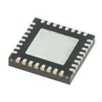


 工商网监
湘ICP备2023018690号
工商网监
湘ICP备2023018690号

