AT9919
Hysteretic Buck High-Brightness LED Driver with High-Side Current Sensing
Features
General Description
•
•
•
•
•
•
•
The AT9919 is a PWM controller IC designed to drive
high-brightness LEDs using a buck topology. It
operates from an input voltage of 4.5 VDC to 40 VDC
and employs hysteretic control with a high-side current
sense resistor to set the constant output current.
Hysteretic Control with High-side Current Sensing
Wide Input Voltage Range: 4.5V to 40V
>90% Efficiency
Typical ±5% LED Current Accuracy
Up to 2 MHz Switching Frequency
Adjustable Constant LED Current
Analog or Pulse-With Modulation (PWM) Control
Signal for PWM Dimming
• Overtemperature Protection
• –40ºC to +125ºC Operating Temperature Range
The operating frequency range can be set by selecting
the proper inductor. Operation at high switching
frequency is possible since the hysteretic control
maintains accuracy even at high frequencies. This
permits the use of small inductors and capacitors,
minimizing space and cost in the overall system.
LED brightness control is achieved with PWM dimming
from an analog or PWM input signal. Unique PWM
circuitry allows true constant color with a high dimming
range. The dimming frequency is programmed using a
single external capacitor.
Applications
• LED Lighting Applications
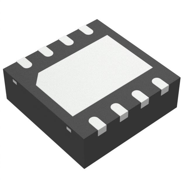
The AT9919 comes in a small, 8-lead DFN package
and is qualified for LED lighting applications.
Package Type
8-lead DFN
(Top View)
CS
1
VIN
2
8
GATE
7
GND
GND
RAMP
3
6
VDD
ADIM
4
5
DIM
See Table 2-1 for pin information.
2016 Microchip Technology Inc.
DS20005595A-page 1
�AT9919
Functional Block Diagram
VIN
VDD
REGULATOR
+
-
CS
CURRENT
SENSE
COMPARATOR
BANDGAP
REF
GATE
DRIVER
GATE
+
DIM
UVLO
COMPARATOR
GND
RAMP
ADIM
DS20005595A-page 2
PWM RAMP
0.1~1.9V
+
AT9919
2016 Microchip Technology Inc.
�AT9919
Typical Application Circuit
RSENSE
L
CIN
VIN
CS
RAMP
0 - 2.0V
ADIM
DIM
VDD
GATE
GND
AT9919
2016 Microchip Technology Inc.
DS20005595A-page 3
�AT9919
1.0
ELECTRICAL CHARACTERISTICS
Absolute Maximum Ratings†
VIN and CS to GND ...................................................................................................................................–0.3V to +45V
VDD, GATE, RAMP, DIM, ADIM to GND......................................................................................................–0.3V to +6V
CS to VIN .....................................................................................................................................................–1V to +0.3V
Operating Temperature Range............................................................................................................. –40°C to +125°C
Junction Temperature.............................................................................................................................................150°C
Storage Temperature Range ...................................................................................................................–65°C to 150°C
Continuous Power Dissipation (TA = +25°C) .......................................................................................................... 1.6W
† Notice: Stresses above those listed under “Absolute Maximum Ratings” may cause permanent damage to the
device. This is a stress rating only, and functional operation of the device at those or any other conditions above those
indicated in the operational sections of this specification is not intended. Exposure to maximum rating conditions for
extended periods may affect device reliability.
ELECTRICAL CHARACTERISTICS
Electrical Specifications: VIN = 12V, VDIM = VDD, VRAMP = GND, CVDD = 1 µF, RCS = 0.5Ω, TA = TJ = –40ºC to
+125ºC (Note 1) unless otherwise noted.
Parameter
Sym.
Min.
Input DC Supply Voltage Range
Internally Regulated Voltage
Supply Current
Shutdown Supply Current
VIN
VDD
IIN
IIN, SDN
Current Limit
IIN, LIM
fOSC
4.5
4.5
—
—
—
—
—
—
—
—
—
30
8
—
40
5.5
1.5
900
—
—
2
MHz
UVLO
—
—
4.5
V
VDD rising
UVLOHYST
—
500
—
mV
VDD falling
VCS(HI)
VCS(LO)
VCS(AVG)
198
147
186
230
170
200
257
195
214
mV
mV
mV
tDPDH
—
70
—
ns
tDPDL
—
70
—
ns
ICS
—
—
1
µA
(VIN – VCS) rising
(VIN – VCS) falling
VCS(AVG) = 0.5VCS(HI) + 0.5VCS(LO)
Falling edge of
VIN – VCS = VRS(LO) – 70 mV
Rising edge of
VIN – VCS = VRS(HI) + 70 mV
VIN – VCS = 200 mV
VCS(HYST)
—
56
80
mV
VIH
VIL
2.2
—
—
—
—
0.7
V
V
Turn-on Time
tON
—
100
—
ns
Turn-off Time
tOFF
—
100
—
ns
Oscillator Frequency
VDD Undervoltage Lockout
Threshold
VDD Undervoltage Lockout
Hysteresis
SENSE COMPARATOR
Sense Voltage Threshold High
Sense Voltage Threshold Low
Average Reference Voltage
Propagation Delay to Output
High
Propagation Delay to Output
Low
Current Sense Input Current
Current Sense Threshold
Hysteresis
DIM INPUT
Pin DIM Input High Voltage
Pin DIM Input Low Voltage
Note 1:
2:
Typ. Max.
Unit
V
V
mA
µA
mA
Conditions
DC input voltage
VIN = 6V to 40V
GATE open
DIM < 0.7V
VIN = 4.5V, VDD = 0V
VIN = 4.5V, VDD = 4V
DIM rising edge to
VGATE = 0.5 x VDD, CGATE = 2 nF
DIM falling edge to
VGATE = 0.5 x VDD, CGATE = 2 nF
Limits obtained by design and characterization.
For design guidance only
DS20005595A-page 4
2016 Microchip Technology Inc.
�AT9919
ELECTRICAL CHARACTERISTICS (CONTINUED)
Electrical Specifications: VIN = 12V, VDIM = VDD, VRAMP = GND, CVDD = 1 µF, RCS = 0.5Ω, TA = TJ = –40ºC to
+125ºC (Note 1) unless otherwise noted.
Parameter
Sym.
Min.
GATE DRIVER
GATE Current, Source
IGATE
GATE Current, Sink
GATE Output Rise Time
TRISE
GATE Output Fall Time
TFALL
GATE High Output Voltage
VGATE(HI)
GATE Low Output Voltage
VGATE(LO)
OVERTEMPERATURE PROTECTION
Over Temperature Trip Limit
TOT
Temperature Hysteresis
∆THYST
ANALOG CONTROL OF PWM DIMMING
Typ. Max.
Conditions
0.3
0.7
—
—
VDD – 0.5
—
0.5
1
40
17
—
—
—
—
55
25
—
0.5
A
A
ns
ns
V
V
VGATE = GND (Note 2)
VGATE = VDD (Note 2)
CGATE = 2 nF
CGATE = 2 nF
IGATE = 10 mA
IGATE = –10 mA
128
—
140
60
—
—
ºC
ºC
Note 2
Note 2
Hz
CRAMP = 47 nF
CRAMP = 10 nF
130
—
550
—
—
0.1
RAMP Threshold, Low
VLOW
RAMP Threshold, High
VHIGH
1.8
—
–35
—
ADIM Offset Voltage
VOS
Note 1: Limits obtained by design and characterization.
2: For design guidance only
Dimming Frequency
Unit
300
1250
—
2.1
+35
fRAMP
V
V
mV
TEMPERATURE SPECIFICATIONS
Parameter
Sym.
Min.
Typ.
Max.
Unit
Operating Temperature
TA
–40
—
+125
°C
Junction Temperature
TJ
—
—
+150
°C
Storage Temperature
TS
–65
—
+150
°C
JA
—
+37
—
°C/W
Conditions
TEMPERATURE RANGE
PACKAGE THERMAL RESISTANCE
8-lead DFN
2016 Microchip Technology Inc.
DS20005595A-page 5
�AT9919
2.0
PIN DESCRIPTION
The details on the pins of AT9919 are listed on
Table 2-1. Refer to Package Type for the location of
pins.
TABLE 2-1:
PIN FUNCTION TABLE
Pin Number
Pin Name
1
CS
Current sense input. Senses LED string current.
2
VIN
Input voltage 4.5V to 40V DC
3
RAMP
4
ADIM
5
DIM
PWM signal input
6
VDD
Internally regulated supply voltage. Connect a capacitor from VDD to ground.
7
GND
Device ground
8
GATE
Drives GATE of the external MOSFET
TAB
GND
Must be wired to pin 7 on PCB
DS20005595A-page 6
Description
Analog PWM dimming ramp output
Analog 0V~2V signal input for analog control of PWM dimming
2016 Microchip Technology Inc.
�AT9919
3.0
APPLICATION INFORMATION
3.1
General Description
The AT9919 is a step-down constant-current
high-brightness LED (HB LED) driver. The device
operates from a 4.5V to 40V input voltage range and
provides the gate drive output to an external N-channel
MOSFET. A high-side current sense resistor sets the
output current, and a dedicated PWM dimming input
(DIM) allows for a wide range of dimming duty ratios.
The PWM dimming could also be achieved by applying
a DC voltage between 0V and 2V to the analog
dimming input (ADIM). In this case, the dimming
frequency can be programmed using a single capacitor
at the RAMP pin. The high-side current sensing
scheme minimizes the number of external components
while delivering LED current with a ±8% accuracy,
using a 1% sense resistor.
3.2
Undervoltage Lockout (UVLO)
The AT9919 includes a 3.7V UVLO with 500 mV
hysteresis. When VIN falls below 3.7V, GATE goes low,
turning off the external N-channel MOSFET. GATE
goes high once VIN is 4.5V or higher.
When the analog control of PWM dimming feature is
not used, RAMP must be wired to GND and ADIM
should be connected to VDD.
One possible application of the ADIM feature may
include protection of the LED load from
overtemperature by connecting an NTC thermistor to
ADIM as shown in Figure 3-1.
VDD
AT9919
ADIM
NTC
GND
FIGURE 3-1:
using ADIM Pin.
3.6
Overtemperature Protection
Setting LED Current with the
External Resistor (RSENSE)
VDD is the output of a 5V regulator capable of sourcing
8 mA. Bypass VDD to GND with a 1 µF capacitor.
The output current in the LED is determined by the
external current sense resistor (RSENSE) connected
between VIN and CS. Disregarding the effect of the
propagation delays, the sense resistor can be
calculated as seen in Equation 3-2.
3.4
EQUATION 3-2:
3.3
5V Regulator
DIM Input
The AT9919 allows dimming with a PWM signal at the
DIM input. A logic level below 0.7V at DIM forces the
GATEOUTPUT low, turning off the LED current. To turn
on the LED current, the logic level at DIM must be at
least 2.2V.
3.5
ADIM and RAMP Inputs
The PWM dimming scheme can also be implemented
by applying an analog control signal to the ADIM pin. If
an analog control signal of 0V~2.0V is applied to ADIM,
the device compares this analog input to a voltage
ramp to pulse width modulate the LED current.
Connecting an external capacitor to RAMP programs
the PWM dimming ramp frequency. See Equation 3-1.
V RS HI + V RS LO
200mV
1
R SENSE --- --------------------------------------------- = ---------------- 2
I LED
I LED
3.7
Selecting Buck Inductor (L)
The AT9919 regulates the LED output current using an
input comparator with hysteresis. (See Figure 3-2.) As
the current through the inductor ramps up, and the
voltage across the sense resistor reaches the upper
threshold, the voltage at GATE goes low, turning off the
external MOSFET. The MOSFET turns on again when
the inductor current ramps down through the
freewheeling diode until the voltage across the sense
resistor equals the lower threshold.
EQUATION 3-1:
1
f PWM = ----------------------------------------C RAMP 120k
The DIM and ADIM inputs can be used simultaneously.
In such case, a fPWM(MAX) lower than the frequency of
the dimming signal at DIM must be selected. The
smaller dimming duty cycle of ADIM and DIM will
determine the GATE signal.
2016 Microchip Technology Inc.
DS20005595A-page 7
�AT9919
tDPDL
VRS(HI)
RSENSE
TS =
1
fS
ILED
VRS(LO)
RSENSE
tDPDH
ΔI
ΔIO
t
VDIM
t
FIGURE 3-2:
Inductor Current Waveform.
Equation 3-3 shows how to determine the inductor
value for a desired operating frequency (fS).
EQUATION 3-3:
V IN – V OUT V OUT V IN – V OUT t DPDL V OUT t DPDH
L = ------------------------------------------------------ – ------------------------------------------------------- – -----------------------------f S V IN I O
I O
I O
Where:
V RS HI – V RS LO
I O = -------------------------------------------R SENSE
and tDPDL and tDPDH are the propagation delays.
Note that the current ripple (∆I) in the inductor (L) is greater than ∆IO.
The current ripple in the inductor (L) can be calculated
with Equation 3-4.
EQUATION 3-4:
V IN – V OUT t DPDL V OUT t DPDH
I = I O + ------------------------------------------------------- + -----------------------------L
L
For proper inductor selection, note that the maximum
switching frequency occurs at the highest VIN and
VOUT = VIN/2.
3.8
MOSFET Selection
MOSFET selection is based on the maximum input
operating voltage VIN, output current ILED and
operating switching frequency. Choose a MOSFET that
has a higher breakdown voltage than the maximum
operation voltage, low RDS(ON) and low total charge for
DS20005595A-page 8
better efficiency. MOSFET threshold voltage must be
adequate when operated at the low end of the input
voltage operating range.
3.9
Freewheeling Diode Selection
The forward voltage of the freewheeling diode should
be as low as possible for better efficiency. A Schottky
diode is a good choice as long as the breakdown
voltage is high enough to withstand the maximum
operating voltage. The forward current rating of the
diode must be at least equal to the maximum LED
current.
3.10
LED Current Ripple
The LED current ripple is equal to the inductor current
ripple. In cases when a lower LED current ripple is
needed, a capacitor can be placed across the LED
terminals.
2016 Microchip Technology Inc.
�AT9919
3.11
PCB Layout Guidelines
Careful PCB layout is critical to achieving low switching
losses and stable operation. Use a multilayer board
whenever possible for better noise immunity. Minimize
ground noise by connecting high-current ground
returns, the input bypass capacitor ground lead and the
output filter ground lead to a single point (star ground
configuration). The fast di/dt loop is composed of the
input capacitor CIN, the freewheeling diode and the
MOSFET. To minimize noise interaction, this loop area
should be as small as possible. Place RSENSE as close
as possible to the input filter and VIN. For better noise
immunity, a Kelvin connection is strongly
recommended between CS and RSENSE. Connect the
exposed tab of the IC to a large area ground plane for
improved power dissipation.
2016 Microchip Technology Inc.
DS20005595A-page 9
�AT9919
4.0
PACKAGING INFORMATION
4.1
Package Marking Information
Legend: XX...X
Y
YY
WW
NNN
e3
*
Note:
DS20005595A-page 10
8-lead DFN
Example
XXXX
YYWW
NNN
9919
1612
373
Product Code or Customer-specific information
Year code (last digit of calendar year)
Year code (last 2 digits of calendar year)
Week code (week of January 1 is week ‘01’)
Alphanumeric traceability code
Pb-free JEDEC® designator for Matte Tin (Sn)
This package is Pb-free. The Pb-free JEDEC designator ( e3 )
can be found on the outer packaging for this package.
In the event the full Microchip part number cannot be marked on one line, it will
be carried over to the next line, thus limiting the number of available
characters for product code or customer-specific information. Package may or
not include the corporate logo.
2016 Microchip Technology Inc.
�AT9919
Note: For the most current package drawings, see the Microchip Packaging Specification at www.microchip.com/packaging.
2016 Microchip Technology Inc.
DS20005595A-page 11
�AT9919
NOTES:
DS20005595A-page 12
2016 Microchip Technology Inc.
�AT9919
APPENDIX A:
REVISION HISTORY
Revision A (October 2016)
• Converted Supertex Doc# DSFP-AT9919 to
Microchip DS20005595A.
• Changed packaging quantity of 8-lead DFN from
3000/Reel to 3300/Reel.
• Made minor text changes throughout the document.
2016 Microchip Technology Inc.
DS20005595A-page 13
�AT9919
PRODUCT IDENTIFICATION SYSTEM
To order or obtain information, e.g., on pricing or delivery, contact your local Microchip representative or sales office.
PART NO.
Device
XX
-
Package
Options
X
-
Environmental
X
Media Type
Device:
AT9919 =
Hysteretic Buck High-Brightness LED
Driver with High-Side Current Sensing
Package:
K7
=
8-lead (3x3) DFN
Environmental:
G
=
Lead (Pb)-free/RoHS-compliant Package
Media Type:
(blank)
=
3300/Reel for a K7 Package
DS20005595A-page 14
Example:
a)
AT9919K7-G:
Hysteretic Buck High-Brightness
LED Driver with High-Side Current
Sensing, 8-lead (3x3) DFN Package, 3300/Reel
2016 Microchip Technology Inc.
�Note the following details of the code protection feature on Microchip devices:
•
Microchip products meet the specification contained in their particular Microchip Data Sheet.
•
Microchip believes that its family of products is one of the most secure families of its kind on the market today, when used in the
intended manner and under normal conditions.
•
There are dishonest and possibly illegal methods used to breach the code protection feature. All of these methods, to our
knowledge, require using the Microchip products in a manner outside the operating specifications contained in Microchip’s Data
Sheets. Most likely, the person doing so is engaged in theft of intellectual property.
•
Microchip is willing to work with the customer who is concerned about the integrity of their code.
•
Neither Microchip nor any other semiconductor manufacturer can guarantee the security of their code. Code protection does not
mean that we are guaranteeing the product as “unbreakable.”
Code protection is constantly evolving. We at Microchip are committed to continuously improving the code protection features of our
products. Attempts to break Microchip’s code protection feature may be a violation of the Digital Millennium Copyright Act. If such acts
allow unauthorized access to your software or other copyrighted work, you may have a right to sue for relief under that Act.
Information contained in this publication regarding device
applications and the like is provided only for your convenience
and may be superseded by updates. It is your responsibility to
ensure that your application meets with your specifications.
MICROCHIP MAKES NO REPRESENTATIONS OR
WARRANTIES OF ANY KIND WHETHER EXPRESS OR
IMPLIED, WRITTEN OR ORAL, STATUTORY OR
OTHERWISE, RELATED TO THE INFORMATION,
INCLUDING BUT NOT LIMITED TO ITS CONDITION,
QUALITY, PERFORMANCE, MERCHANTABILITY OR
FITNESS FOR PURPOSE. Microchip disclaims all liability
arising from this information and its use. Use of Microchip
devices in life support and/or safety applications is entirely at
the buyer’s risk, and the buyer agrees to defend, indemnify and
hold harmless Microchip from any and all damages, claims,
suits, or expenses resulting from such use. No licenses are
conveyed, implicitly or otherwise, under any Microchip
intellectual property rights unless otherwise stated.
Microchip received ISO/TS-16949:2009 certification for its worldwide
headquarters, design and wafer fabrication facilities in Chandler and
Tempe, Arizona; Gresham, Oregon and design centers in California
and India. The Company’s quality system processes and procedures
are for its PIC® MCUs and dsPIC® DSCs, KEELOQ® code hopping
devices, Serial EEPROMs, microperipherals, nonvolatile memory and
analog products. In addition, Microchip’s quality system for the design
and manufacture of development systems is ISO 9001:2000 certified.
QUALITY MANAGEMENT SYSTEM
CERTIFIED BY DNV
== ISO/TS 16949 ==
2016 Microchip Technology Inc.
Trademarks
The Microchip name and logo, the Microchip logo, AnyRate,
dsPIC, FlashFlex, flexPWR, Heldo, JukeBlox, KeeLoq,
KeeLoq logo, Kleer, LANCheck, LINK MD, MediaLB, MOST,
MOST logo, MPLAB, OptoLyzer, PIC, PICSTART, PIC32 logo,
RightTouch, SpyNIC, SST, SST Logo, SuperFlash and UNI/O
are registered trademarks of Microchip Technology
Incorporated in the U.S.A. and other countries.
ClockWorks, The Embedded Control Solutions Company,
ETHERSYNCH, Hyper Speed Control, HyperLight Load,
IntelliMOS, mTouch, Precision Edge, and QUIET-WIRE are
registered trademarks of Microchip Technology Incorporated
in the U.S.A.
Analog-for-the-Digital Age, Any Capacitor, AnyIn, AnyOut,
BodyCom, chipKIT, chipKIT logo, CodeGuard, dsPICDEM,
dsPICDEM.net, Dynamic Average Matching, DAM, ECAN,
EtherGREEN, In-Circuit Serial Programming, ICSP, Inter-Chip
Connectivity, JitterBlocker, KleerNet, KleerNet logo, MiWi,
motorBench, MPASM, MPF, MPLAB Certified logo, MPLIB,
MPLINK, MultiTRAK, NetDetach, Omniscient Code
Generation, PICDEM, PICDEM.net, PICkit, PICtail,
PureSilicon, RightTouch logo, REAL ICE, Ripple Blocker,
Serial Quad I/O, SQI, SuperSwitcher, SuperSwitcher II, Total
Endurance, TSHARC, USBCheck, VariSense, ViewSpan,
WiperLock, Wireless DNA, and ZENA are trademarks of
Microchip Technology Incorporated in the U.S.A. and other
countries.
SQTP is a service mark of Microchip Technology Incorporated
in the U.S.A.
Silicon Storage Technology is a registered trademark of
Microchip Technology Inc. in other countries.
GestIC is a registered trademarks of Microchip Technology
Germany II GmbH & Co. KG, a subsidiary of Microchip
Technology Inc., in other countries.
All other trademarks mentioned herein are property of their
respective companies.
© 2016, Microchip Technology Incorporated, Printed in the
U.S.A., All Rights Reserved.
ISBN: 978-1-5224-0992-2
DS20005595A-page 15
�Worldwide Sales and Service
AMERICAS
ASIA/PACIFIC
ASIA/PACIFIC
EUROPE
Corporate Office
2355 West Chandler Blvd.
Chandler, AZ 85224-6199
Tel: 480-792-7200
Fax: 480-792-7277
Technical Support:
http://www.microchip.com/
support
Web Address:
www.microchip.com
Asia Pacific Office
Suites 3707-14, 37th Floor
Tower 6, The Gateway
Harbour City, Kowloon
China - Xiamen
Tel: 86-592-2388138
Fax: 86-592-2388130
Austria - Wels
Tel: 43-7242-2244-39
Fax: 43-7242-2244-393
China - Zhuhai
Tel: 86-756-3210040
Fax: 86-756-3210049
Denmark - Copenhagen
Tel: 45-4450-2828
Fax: 45-4485-2829
India - Bangalore
Tel: 91-80-3090-4444
Fax: 91-80-3090-4123
France - Paris
Tel: 33-1-69-53-63-20
Fax: 33-1-69-30-90-79
India - New Delhi
Tel: 91-11-4160-8631
Fax: 91-11-4160-8632
Germany - Dusseldorf
Tel: 49-2129-3766400
Atlanta
Duluth, GA
Tel: 678-957-9614
Fax: 678-957-1455
Hong Kong
Tel: 852-2943-5100
Fax: 852-2401-3431
Australia - Sydney
Tel: 61-2-9868-6733
Fax: 61-2-9868-6755
China - Beijing
Tel: 86-10-8569-7000
Fax: 86-10-8528-2104
Austin, TX
Tel: 512-257-3370
China - Chengdu
Tel: 86-28-8665-5511
Fax: 86-28-8665-7889
Boston
Westborough, MA
Tel: 774-760-0087
Fax: 774-760-0088
China - Chongqing
Tel: 86-23-8980-9588
Fax: 86-23-8980-9500
Chicago
Itasca, IL
Tel: 630-285-0071
Fax: 630-285-0075
Cleveland
Independence, OH
Tel: 216-447-0464
Fax: 216-447-0643
Dallas
Addison, TX
Tel: 972-818-7423
Fax: 972-818-2924
Detroit
Novi, MI
Tel: 248-848-4000
Houston, TX
Tel: 281-894-5983
Indianapolis
Noblesville, IN
Tel: 317-773-8323
Fax: 317-773-5453
Los Angeles
Mission Viejo, CA
Tel: 949-462-9523
Fax: 949-462-9608
New York, NY
Tel: 631-435-6000
San Jose, CA
Tel: 408-735-9110
Canada - Toronto
Tel: 905-695-1980
Fax: 905-695-2078
China - Dongguan
Tel: 86-769-8702-9880
China - Guangzhou
Tel: 86-20-8755-8029
China - Hangzhou
Tel: 86-571-8792-8115
Fax: 86-571-8792-8116
China - Hong Kong SAR
Tel: 852-2943-5100
Fax: 852-2401-3431
China - Nanjing
Tel: 86-25-8473-2460
Fax: 86-25-8473-2470
China - Qingdao
Tel: 86-532-8502-7355
Fax: 86-532-8502-7205
China - Shanghai
Tel: 86-21-5407-5533
Fax: 86-21-5407-5066
China - Shenyang
Tel: 86-24-2334-2829
Fax: 86-24-2334-2393
China - Shenzhen
Tel: 86-755-8864-2200
Fax: 86-755-8203-1760
India - Pune
Tel: 91-20-3019-1500
Japan - Osaka
Tel: 81-6-6152-7160
Fax: 81-6-6152-9310
Japan - Tokyo
Tel: 81-3-6880- 3770
Fax: 81-3-6880-3771
Korea - Daegu
Tel: 82-53-744-4301
Fax: 82-53-744-4302
Korea - Seoul
Tel: 82-2-554-7200
Fax: 82-2-558-5932 or
82-2-558-5934
Malaysia - Kuala Lumpur
Tel: 60-3-6201-9857
Fax: 60-3-6201-9859
Malaysia - Penang
Tel: 60-4-227-8870
Fax: 60-4-227-4068
Philippines - Manila
Tel: 63-2-634-9065
Fax: 63-2-634-9069
Germany - Karlsruhe
Tel: 49-721-625370
Germany - Munich
Tel: 49-89-627-144-0
Fax: 49-89-627-144-44
Italy - Milan
Tel: 39-0331-742611
Fax: 39-0331-466781
Italy - Venice
Tel: 39-049-7625286
Netherlands - Drunen
Tel: 31-416-690399
Fax: 31-416-690340
Poland - Warsaw
Tel: 48-22-3325737
Spain - Madrid
Tel: 34-91-708-08-90
Fax: 34-91-708-08-91
Sweden - Stockholm
Tel: 46-8-5090-4654
UK - Wokingham
Tel: 44-118-921-5800
Fax: 44-118-921-5820
Singapore
Tel: 65-6334-8870
Fax: 65-6334-8850
Taiwan - Hsin Chu
Tel: 886-3-5778-366
Fax: 886-3-5770-955
Taiwan - Kaohsiung
Tel: 886-7-213-7828
China - Wuhan
Tel: 86-27-5980-5300
Fax: 86-27-5980-5118
Taiwan - Taipei
Tel: 886-2-2508-8600
Fax: 886-2-2508-0102
China - Xian
Tel: 86-29-8833-7252
Fax: 86-29-8833-7256
Thailand - Bangkok
Tel: 66-2-694-1351
Fax: 66-2-694-1350
06/23/16
DS20005595A-page 16
2016 Microchip Technology Inc.
�


 工商网监
湘ICP备2023018690号
工商网监
湘ICP备2023018690号
