ATA6614Q
32K Flash Microcontroller with LIN Transceiver, 5V
Regulator and Watchdog
DATASHEET
General Features
● Single-package fully-integrated AVR® 8-bit microcontroller with LIN transceiver,
5V regulator (85mA current capability) and watchdog
● Very low current consumption in sleep mode
● 32Kbytes flash memory for application program
● Supply voltage up to 40V
● Operating voltage: 5V to 27V
● Temperature range: Tcase –40°C to +125°C
● QFN48, 7mm 7mm package
9240I-AUTO-03/16
�1.
Description
Atmel® ATA6614Q is a system-in-package (SiP) product, which is particularly suited for complete LIN-bus slave-node
applications. It consists of two ICs in one package supporting highly integrated solutions for in-vehicle LIN networks. The first
chip is the LIN-system-basis-chip (LIN-SBC) Atmel ATA6630, which has an integrated LIN transceiver, a 5V regulator
(85mA) and a window watchdog. The second chip is an automotive microcontroller from Atmel’s series of AVR® 8-bit
microcontroller with advanced RISC architecture and 32Kbytes of flash (Atmel ATmega328P). All pins of the AVR
microcontroller and almost all pins of the LIN System Basis Chip are bonded out to provide customers the same flexibility for
their applications as they have when using discrete parts.
The Atmel ATA6614Q is pin compatible to the Atmel ATA6612P/ATA6613P.
In Section 2. “Pin Configuration” on page 3 you will find the pin configuration for the complete SiP. In Section 3. “Absolute
Maximum Ratings” on page 5 to Section 5. “Microcontroller Block” on page 30 the LIN SBC is described, and in Section 7.
“Ordering Information” on page 307 the AVR is described in detail.
Figure 1-1. Application Diagram
LIN Bus
Atmel ATA6614Q
MCU
Atmel
ATmega328P
2
ATA6614Q [DATASHEET]
9240I–AUTO–03/16
LIN-SBC
Atmel
ATA6630
�Pin Configuration
PB4
PB3
PB2
PB1
PB0
PD7
PD6
PD5
PB7
PB6
MCUVCC
GND2
Figure 2-1. Pinning QFN48, 7mm 7mm
PB5
MCUAVCC
ADC6
AREF
GND4
ADC7
PC0
PC1
PC2
PC3
PC4
PC5
1
48 47 46 45 44 43 42 41 40 39 38 37
36
2
35
3
34
4
33
5
32
6
31
7
30
8
29
9
28
10
27
11
26
25
12
13 14 15 16 17 18 19 20 21 22 23 24
MCUVCC
GND1
PD4
PD3
LIN
GND
WAKE
NTRIG
EN
VS
VCC
PVCC
PC6
PD0
PD1
PD2
RXD
INH
TXD
NRES
WD_OSC
TM
MODE
KL_15
2.
Table 2-1.
Pin Description
Pin
Symbol
1
PB5
2
MCUAVCC
3
ADC6
ADC input channel 6
4
AREF
Analog reference voltage input
5
GND
Ground
6
ADC7
ADC input channel 7
7
PC0
Port C 0 I/O line (ADC0/PCINT8)
8
PC1
Port C 1 I/O line (ADC1/PCINT9)
9
PC2
Port C 2 I/O line (ADC2/PCINT10)
10
PC3
Port C 3 I/O line (ADC3/PCINT11)
11
PC4
Port C 4 I/O line (ADC4/SDA/PCINT12)
12
PC5
Port C 5 I/O line (ADC5/SCL/PCINT13)
13
PC6
Port C 6 I/O line (RESET/PCINT14)
14
PD0
Port D 0 I/O line (RXD/PCINT16)
15
PD1
Port D 1 I/O line (TXD/PCINT17)
16
PD2
Port D 2 I/O line (INT0/PCINT18)
RXD
Receive data output
(1)
17
(1)
18
Note:
1.
Function
Port B 5 I/O line (SCK / PCINT5)
Microcontroller ADC-unit supply voltage (referred to as AVCC pin in Section 5. “Microcontroller
Block” on page 30)
INH
High side switch output for controlling an external voltage regulator
This identifies the pins of the LIN SBC ATA6630
ATA6614Q [DATASHEET]
9240I–AUTO–03/16
3
�Table 2-1.
Pin Description (Continued)
Pin
Symbol
(1)
19
TXD
20(1)
NRES
Transmit data input, active low output (strong pull down)
Watchdog and undervoltage reset output (open drain)
(1)
WD_OSC
(1)
TM
(1)
23
MODE
Connect to GND for normal watchdog operation or connect to VCC for disabling the watchdog
24(1)
KL_15
Ignition detection (edge sensitive)
(1)
PVCC
Voltage regulator sense input
(1)
VCC
21
22
25
26
External resistor for adjustable watchdog timing
Tie to Ground – for factory use only
Voltage regulator output
(1)
27
VS
Battery supply voltage
28(1)
EN
Enables the device into normal mode
(1)
NTRIG
Watchdog trigger input (negative edge)
(1)
WAKE
High voltage input for local wake-up request
(1)
29
30
31
AGND
Analog system GND
32(1)
LIN
LIN bus input/output
33
PD3
Port D 3 I/O line (INT1 OC2B/PCINT19)
34
PD4
Port D 4 I/O line (T0/XCK/PCINT20)
35
GND1
36
MCUVCC
37
GND2
38
MCUVCC
39
PB6
Port B 6 I/O line (TOSC1/XTAL1/PCINT6)
40
PB7
Port B 7 I/O line (TOSC2/XTAL2/PCINT7)
41
PD5
Port D 5 I/O line (T1/OC0B/PCINT21)
42
PD6
Port D 6 I/O line (AIN0/OC0A PCINT22)
43
PD7
Port D 7 I/O line (AIN1/PCINT23)
44
PB0
Port B 0 I/O line (ICP1/CLKO/PCINT0)
45
PB1
Port B 1 I/O line (OC1A/PCINT1)
46
PB2
Port B 2 I/O line (OC1B/SS/PCINT2)
47
PB3
Port B 3 I/O line (MOSI/OC2A/PCINT3)
48
PB4
Port B 4 I/O line (MISO/PCINT4)
Backside
Note:
1.
4
Function
Ground
Microcontroller supply voltage (referred to as VCC pin in Section 5. “Microcontroller Block” on
page 30)
Ground
Microcontroller supply voltage (referred to as VCC pin in Section 5. “Microcontroller Block” on
page 30)
Heat slug is connected to GND
This identifies the pins of the LIN SBC ATA6630
ATA6614Q [DATASHEET]
9240I–AUTO–03/16
�3.
Absolute Maximum Ratings
Table 3-1.
Maximum Ratings of the SiP
Stresses beyond those listed under “Absolute Maximum Ratings” may cause permanent damage to the device. This is a stress rating
only and functional operation of the device at these or any other conditions beyond those indicated in the operational sections of this
specification is not implied. Exposure to absolute maximum rating conditions for extended periods may affect device reliability.
Parameters
Symbol
HBM ESD
ANSI/ESD-STM5.1
JESD22-A114
AEC-Q100 (002)
Min.
Typ.
Max.
Unit
±2
KV
CDM ESD STM 5.3.1
±750
V
Machine Model ESD AEC-Q100-Rev.F (003)
±100
V
ESD according to IBEE LIN EMC
Test Spec. 1.0 following IEC 61000-4-2
- Pin VS, LIN to GND
- Pin WAKE (2.7k serial resistor) to GND
- KL_15 (47k/100nF) to GND
±8
KV
ESD HBM following STM5.1 with 1.5k 100pF
- Pin VS, LIN, KL_15, WAKE to GND
±6
KV
Storage temperature
Operating temperature
(1)
Ts
–55
+150
°C
Tcase
–40
+125
°C
Thermal resistance junction to heat slug
Rthjc
5
K/W
Thermal resistance junction to ambient
Rthja
25
K/W
Thermal shutdown of VCC regulator
150
165
170
°C
Thermal shutdown of LIN output
150
165
170
°C
Thermal shutdown hysteresis
10
°C
Note:
1. Tcase means the temperature of the heat slug (backside). It is mandatory that this backside temperature is ≤ 125°C in
the application.
Table 3-2.
Maximum Ratings of the LIN-SBC
Stresses beyond those listed under “Absolute Maximum Ratings” may cause permanent damage to the device. This is a stress rating
only and functional operation of the device at these or any other conditions beyond those indicated in the operational sections of this
specification is not implied. Exposure to absolute maximum rating conditions for extended periods may affect device reliability.
Parameters
Symbol
Min.
Supply voltage VS
VS
–0.3
Pulse time ≤ 500ms; Ta = 25°C
Output current IVCC ≤ 85mA
Pulse time ≤ 2min; Ta = 25°C
Output current IVCC ≤ 85mA
Max.
Unit
+40
V
VS
+40
V
VS
27
V
–1
–150
+40
+100
V
V
INH
- DC voltage
–0.3
VS + 0.3
V
LIN
- DC voltage
–27
+40
V
WAKE (with 2.7k serial resistor)
KL_15 (with 47k/100nF)
DC voltage
Transient voltage due to ISO7637 (coupling 1nF)
Typ.
ATA6614Q [DATASHEET]
9240I–AUTO–03/16
5
�Table 3-2.
Maximum Ratings of the LIN-SBC (Continued)
Stresses beyond those listed under “Absolute Maximum Ratings” may cause permanent damage to the device. This is a stress rating
only and functional operation of the device at these or any other conditions beyond those indicated in the operational sections of this
specification is not implied. Exposure to absolute maximum rating conditions for extended periods may affect device reliability.
Parameters
Symbol
Logic pins (RXD, TXD, EN, NRES, NTRIG,
WD_OSC, MODE, TM)
Output current NRES
Typ.
Max.
Unit
–0.3
VCC + 0.5
V
+2
mA
–0.3
–0.3
+5.5
+6.5
V
V
INRES
PVCC DC voltage
VCC DC voltage
Table 3-3.
Min.
Maximum Ratings of the Microcontroller
Stresses beyond those listed under “Absolute Maximum Ratings” may cause permanent damage to the device. This is a stress rating
only and functional operation of the device at these or any other conditions beyond those indicated in the operational sections of this
specification is not implied. Exposure to absolute maximum rating conditions for extended periods may affect device reliability.
Parameters
Symbol
Min.
Typ.
Max.
Unit
Voltage on any Pin except RESET with respect to
Ground
–0.5
MCUVCC +
0.5
V
Voltage on RESET with respect to Ground
–0.5
13.0
V
Maximum Operating Voltage
6.0
V
DC Current per I/O Pin
40.0
mA
200.0
mA
Injection Current at MCUVCC = 0V
±5.0
mA
Injection Current at MCUVCC = 5V
Note:
1. Maximum current per port = ±30mA
±1.0
mA
DC Current MCUVCC and GND Pins
(1)
6
ATA6614Q [DATASHEET]
9240I–AUTO–03/16
�4.
LIN System-basis-chip Block
4.1
Features
●
●
●
●
●
●
Master and slave operation possible
Supply voltage up to 40V
Operating voltage VS = 5V to 27V
Typically 10µA supply current during sleep mode
Typically 35µA supply current in silent mode
Linear low-drop voltage regulator, 85mA current capability:
●
Normal, fail-safe, and silent mode
●
In sleep mode VCC is switched off
●
●
●
●
●
●
●
●
●
●
●
●
●
4.2
VCC = 5.0V ±2%
VCC undervoltage detection (4ms reset time) and watchdog reset logical combined at open drain output NRES
Negative trigger input for watchdog
Adjustable watchdog time via external resistor
Boosting the voltage regulator possible with an external NPN transistor
LIN physical layer according to LIN 2.0, 2.1 and SAEJ2602-2
Wake-up capability via LIN-bus, wake pin, or Kl_15 pin
INH output to control an external voltage regulator or to switch off the master pull up resistor
TXD time-out timer
Bus pin is overtemperature and short-circuit protected versus GND and battery
Advanced EMC and ESD performance
Fulfills the OEM “Hardware Requirements for LIN in Automotive Applications Rev.1.1”
Interference and damage protection according to ISO7637
Description
The Atmel® ATA6630 is a fully integrated LIN transceiver, which complies with the LIN 2.0, 2.1 and SAEJ2602-2
specifications. It has a low-drop voltage regulator for 5V/85mA output and a window watchdog. The voltage regulator is able
to source up to 85mA, but the output current can be boosted by using an external NPN transistor. The Atmel ATA6630 is
designed to handle the low-speed data communication in vehicles, e.g., in convenience electronics. Improved slope control
at the LIN-driver ensures secure data communication up to 20kBaud. Sleep Mode and Silent Mode guarantee very low
current consumption.
ATA6614Q [DATASHEET]
9240I–AUTO–03/16
7
�Figure 4-1. Block Diagram SBC
VS
Normal and
Fail-safe
Mode
INH
PVCC
Normal
Mode
Receiver
RXD
+
RF Filter
LIN
WAKE
KL_15
PVCC
TXD
Edge
Detection
Wake-up
Bus Timer
Slew Rate Control
TXD
Time-out
Timer
Control Unit
EN
Short Circuit and
Overtemperature
Protection
Debounce
Time
Normal/Silent/
Fail-safe Mode
5V
Undervoltage
Reset
OUT
Watchdog
GND
PVCC
8
ATA6614Q [DATASHEET]
9240I–AUTO–03/16
PVCC
Mode Select
Internal Testing
Unit
MODE
VCC
TM
NTRIG
NRES
Adjustable
Watchdog
Oscillator
WD_OSC
�4.3
Functional Description
4.3.1
Physical Layer Compatibility
Since the LIN physical layer is independent from higher LIN layers (e.g., the LIN protocol layer), all nodes with a LIN physical
layer according to revision 2.x can be mixed with LIN physical layer nodes, which are, according to older versions (i.e., LIN
1.0, LIN 1.1, LIN 1.2, LIN 1.3), without any restrictions.
4.3.2
Supply Pin (VS)
The LIN operating voltage is VS = 5V to 27V. An undervoltage detection is implemented to disable data transmission if VS
falls below VSth in order to avoid false bus messages. After switching on VS, the IC starts in fail-safe mode, and the voltage
regulator is switched on (5V/85mA output capability).
The supply current is typically 10µA in sleep mode and 35µA in silent mode.
4.3.3
Ground Pin (GND)
The IC does not affect the LIN Bus in the event of GND disconnection. It is able to handle a ground shift up to 11.5% of
versus The mandatory system ground is pin 5.
4.3.4
Voltage Regulator Output Pin (VCC)
The internal 3.3V/5V voltage regulator is capable of driving loads up to 50mA. It is able to supply the microcontroller and
other ICs on the PCB and is protected against overloads by means of current limitation and overtemperature shut-down.
Furthermore, the output voltage is monitored and will cause a reset signal at the NRES output pin if it drops below a defined
threshold Vthun. To boost up the maximum load current, an external NPN transistor may be used, with its base connected to
the VCC pin and its emitter connected to PVCC.
4.3.5
Voltage Regulator Sense Pin (PVCC)
The PVCC is the sense input pin of the 5V voltage regulator. For normal applications (i.e., when only using the internal
output transistor), this pin must be connected to the VCC pin. If an external boosting transistor is used, the PVCC pin must
be connected to the output of this transistor, i.e., its emitter terminal.
4.3.6
Bus Pin (LIN)
A low-side driver with internal current limitation and thermal shutdown and an internal pull-up resistor compliant with the LIN
2.x specification are implemented. The allowed voltage range is between –27V and +40V. Reverse currents from the LIN
bus to VS are suppressed, even in the event of GND shifts or battery disconnection. LIN receiver thresholds are compatible
with the LIN protocol specification. The fall time from recessive to dominant bus state and the rise time from dominant to
recessive bus state are slope controlled.
4.3.7
Input/Output Pin (TXD)
In normal mode the TXD pin is the microcontroller interface used to control the state of the LIN output. TXD must be pulled to
ground in order to have a low LIN-bus. If TXD is high or not connected (internal pull-up resistor), the LIN output transistor is
turned off, and the bus is in recessive state. During Fail-safe Mode, this pin is used as output and is signalling the fail-safe
source (together with the RXD output). It is current-limited to < 8mA.
4.3.8
TXD Dominant Time-out Function
The TXD input has an internal pull-up resistor. An internal timer prevents the bus line from being driven permanently in
dominant state. If TXD is forced to low for longer than tDOM > 27ms, the LIN-bus driver is switched to recessive state.
Nevertheless, when switching to sleep mode, the actual level at the TXD pin is relevant.
To reactivate the LIN bus driver, switch TXD to high (> 10µs).
ATA6614Q [DATASHEET]
9240I–AUTO–03/16
9
�4.3.9
Output Pin (RXD)
This output pin reports the state of the LIN-bus to the microcontroller. LIN high (recessive state) is reported by a high level at
RXD; LIN low (dominant state) is reported by a low level at RXD. The output has an internal pull-up resistor with typically
5k to PVCC. The AC characteristics can be defined with an external load capacitor of 20pF.
The output is short-circuit protected. RXD is switched off in Unpowered Mode (i.e., VS = 0V).
During Fail-safe Mode it is signalling the fail-safe source (together with the TXD- pin).
4.3.10 Enable Input Pin (EN)
The Enable Input pin controls the operation mode of the device. If EN is high, the circuit is in Normal Mode, with transmission
paths from TXD to LIN and from LIN to RXD both active. The VCC voltage regulator operates with 5V/85mA output
capability.
If EN is switched to low while TXD is still high, the device is forced to Silent Mode. No data transmission is then possible, and
the current consumption is reduced to IVSsilent typ. 35µA. The VCC regulator has its full functionality.
If EN is switched to low while TXD is low, the device is forced to Sleep Mode. No data transmission is possible, and the
voltage regulator is switched off.
4.3.11 Wake Input Pin (WAKE)
The WAKE Input pin is a high-voltage input used to wake up the device from Sleep Mode or Silent Mode. It is usually
connected to an external switch in the application to generate a local wake-up. A pull-up current source, typically 10µA, is
implemented.
If a local wake-up is not needed in the application, connect the WAKE pin directly to the VS pin.
4.3.12 Mode Input Pin (MODE)
Connect the MODE pin directly or via an external resistor to GND for normal watchdog operation. To debug the software of
the connected microcontroller, connect the MODE pin to VCC and the watchdog is switched off.
4.3.13 TM Input Pin
The TM pin is used for final production measurements at Atmel®. In normal application, it has to be always connected to
GND.
4.3.14 KL_15 Pin
The KL_15 pin is a high-voltage input used to wake up the device from Sleep or Silent Mode. It is an edge-sensitive pin (lowto-high transition). It is usually connected to ignition to generate a local wake-up in the application when the ignition is
switched on. Although KL_15 pin is at high voltage (VBatt), it is possible to switch the IC into Sleep or Silent Mode. Connect
the KL_15 pin directly to GND if you do not need it. A debounce timer with a typical TdbKl_15 of 160µs is implemented.
The input voltage threshold can be adjusted by varying the external resistor due to the input current IKL_15. To protect this pin
against voltage transients, a serial resistor of 47k and a ceramic capacitor of 100nF are recommended. With this RC
combination you can increase the wake-up time TwKL_15 and, therefore, the sensitivity against transients on the ignition
KL_15.
The wake-up time can also be increased by using external capacitors with higher values.
4.3.15 INH Output Pin
The INH Output pin is used to switch on an external voltage regulator during Normal and Fail-safe Mode. The INH Output is
a high-side switch, which is switched-off in Sleep and Silent Mode. It is possible to switch off the external 1k master resistor
via the INH pin for master node applications.
4.3.16 Wake-up Events from Sleep or Silent Mode
●
●
●
●
10
LIN-bus
WAKE pin
EN pin
KL_15
ATA6614Q [DATASHEET]
9240I–AUTO–03/16
�4.3.17
Reset Output Pin (NRES)
The Reset Output pin, an open drain output, switches to low during VCC undervoltage or a watchdog failure.
4.3.18 WD_OSC Output Pin
The WD_OSC Output pin provides a typical voltage of 1.2V, which supplies an external resistor with values between 34k
and 120k to adjust the watchdog oscillator time.
4.3.19 NTRIG Input Pin
The NTRIG Input pin is the trigger input for the window watchdog. A pull-up resistor is implemented.
A negative edge triggers the watchdog. The trigger signal (low) must exceed a minimum time ttrigmin to generate a watchdog
trigger.
4.4
Modes of Operation
Figure 4-2. Modes of Operation
a: VS > 5V
Unpowered Mode
VBatt = 0V
b
b: VS < 4V
c: Bus wake-up event
d: Wake up from WAKE or KL_15 pin
a
e: NRES switches to low
b
Fail-safe Mode
VCC: 5V
With undervoltage monitoring
Communication: OFF
Watchdog: ON
b
e
EN = 1
b
c+d+e
EN = 1
c+d
Go to silent command
EN = 0
Silent Mode
TXD = 1
Normal Mode
VCC: 5V
With undervoltage
monitoring
Communication: ON
Watchdog: ON
Table 4-1.
VCC: 5V
With undervoltage monitoring
Communication: OFF
Watchdog: OFF
Local wake-up event
EN = 1
Go to sleep command
EN = 0
Sleep Mode
TXD = 0
VCC: switched off
Communication: OFF
Watchdog: OFF
Table of Modes
Mode of
Operation
Transceiver
Pin LIN
VCC
Pin Mode
Watchdog
Pin WD_OSC
Pin INH
Unpowered
Off
Recessive
On
GND
On
On
Off
Fail-safe
Off
Recessive
5V
GND
On
1.23V
On
Normal
On
TXD depending
5V
GND
On
1.23V
On
Silent
Off
Recessive
5V
GND
Off
0V
Off
Sleep
Off
Recessive
0V
GND
Off
0V
Off
ATA6614Q [DATASHEET]
9240I–AUTO–03/16
11
�4.4.1
Normal Mode
This is the normal transmitting and receiving mode. The voltage regulator is active and can source up to 85mA. The
undervoltage detection is activated. The watchdog needs a trigger signal from NTRIG to avoid resets at NRES. If NRES is
switched to low, the IC changes its state to Fail-safe Mode.
4.4.2
Silent Mode
A falling edge at EN when TXD is high switches the IC into Silent Mode. The TXD Signal has to be logic high during the
Mode Select window (see Figure 4-3 on page 12). The transmission path is disabled in Silent Mode. The INH output is
switched off and the voltage divider is enabled. The overall supply current from VBatt is a combination of the IVSsi = 35µA plus
the VCC regulator output current IVCC.
The 5V regulator with 2% tolerance can source up to 85mA. The internal slave termination between the LIN pin and the VS
pin is disabled in Silent Mode to minimize the current consumption in the event that the LIN pin is short-circuited to GND.
Only a weak pull-up current (typically 10µA) between the LIN pin and the VS pin is present. Silent Mode can be activated
independently from the actual level on the LIN, WAKE, or KL_15 pins. If an undervoltage condition occurs, NRES is switched
to low and the IC changes its state to Fail-safe Mode.
A voltage lower than the LIN Pre_Wake detection VLINL at the LIN pin activates the internal LIN receiver and starts the
wake-up detection timer.
Figure 4-3. Switch to Silent Mode
Normal Mode
Silent Mode
EN
TXD
Mode select window
td = 3.2μs
NRES
VCC
Delay time silent mode
td_sleep = maximum 20μs
LIN
LIN switches directly to recessive mode
12
ATA6614Q [DATASHEET]
9240I–AUTO–03/16
�A falling edge at the LIN pin followed by a dominant bus level maintained for a certain time period (>tbus) and followed by a
rising edge at the LIN pin (see Figure 4-4 on page 13) result in a remote wake-up request which is only possible if TXD is
high. The device switches from Silent Mode to Fail-safe Mode. The internal LIN slave termination resistor is switched on. The
remote wake-up request is indicated by a low level at the RXD pin to interrupt the microcontroller (see Figure 4-4 on page
13). EN high can be used to switch directly to Normal Mode.
Figure 4-4. LIN Wake Up from Silent Mode
Bus wake-up filtering time
tbus
Fail-safe mode
Normal mode
LIN bus
Node in silent mode
RXD
High
Low
High
TXD
Watchdog
VCC
voltage
regulator
Watchdog off
Start watchdog lead time td
Silent mode 5V
Fail safe mode 5V
Normal mode
EN High
EN
NRES
Undervoltage detection active
ATA6614Q [DATASHEET]
9240I–AUTO–03/16
13
�4.4.3
Sleep Mode
A falling edge at EN when TXD is low switches the IC into Sleep Mode. The TXD Signal has to be logic low during the Mode
Select window (Figure 4-5 on page 14). In order to avoid any influence to the LIN-pin during switching into sleep mode it is
possible to switch the EN up to 3.2µs earlier to Low than the TXD. Therefore, the best an easiest way are two falling edges
at TXD and EN at the same time. The transmission path is disabled in Sleep Mode. The supply current IVSsleep from VBatt is
typically 10µA.
The INH output and the VCC regulator are switched off. NRES and RXD are low. The internal slave termination between the
LIN pin and VS pin is disabled to minimize the current consumption in the event that the LIN pin is short-circuited to GND.
Only a weak pull-up current (typically 10µA) between the LIN pin and the VS pin is present. Sleep Mode can be activated
independently from the current level on the LIN, WAKE, or KL_15 pin.
A voltage lower than the LIN Pre_Wake detection VLINL at the LIN pin activates the internal LIN receiver and starts the
wake-up detection timer.
Figure 4-5. Switch to Sleep Mode
Normal Mode
Sleep Mode
EN
Mode select window
TXD
td = 3.2μs
NRES
VCC
Delay time sleep mode
td_sleep = maximum 20μs
LIN
LIN switches directly to recessive mode
14
ATA6614Q [DATASHEET]
9240I–AUTO–03/16
�A falling edge at the LIN pin followed by a dominant bus level maintained for a certain time period (>tbus) and a rising edge at
pin LIN result in a remote wake-up request. The device switches from Sleep Mode to Fail-safe Mode.
The VCC regulator is activated, and the internal LIN slave termination resistor is switched on. The remote wake-up re-quest
is indicated by a low level at the RXD pin to interrupt the microcontroller (see Figure 4-6 on page 15).
EN high can be used to switch directly from Sleep/Silent to Fail-safe Mode. If EN is still high after VCC ramp up and
undervoltage reset time, the IC switches to the Normal Mode.
Figure 4-6. LIN Wake Up from Sleep Mode
Bus wake-up filtering time
tbus
Fail-safe Mode
Normal Mode
LIN bus
RXD
Low
TXD
VCC
voltage
regulator
On state
Off state
Regulator wake-up time
EN High
EN
Reset
time
NRES
Microcontroller
start-up time delay
Watchdog
Watchdog off
Start watchdog lead time td
ATA6614Q [DATASHEET]
9240I–AUTO–03/16
15
�4.4.4
Sleep or Silent Mode: Behavior at a Floating LIN-bus or a Short Circuited LIN to GND
In Sleep or in Silent Mode the device has a very low current consumption even during short-circuits or floating conditions on
the bus. A floating bus can arise if the Master pull-up resistor is missing, e.g., if it is switched off when the LIN-Master is in
sleep mode or even if the power supply of the Master node is switched off.
In order to minimize the current consumption IVS in sleep or silent mode during voltage levels at the LIN-pin below the LIN
pre-wake threshold, the receiver is activated only for a specific time tmon. If tmon elapses while the voltage at the bus is lower
than the Pre-wake detection low (VLINL) and higher than the LIN dominant level, the receiver is switched off again and the
circuit changes back to sleep respectively Silent Mode. The current consumption is then IVSsleep_short or IVSsilent_short (typ. 10µA
more than IVSsleep respectively IVSsilent). If a dominant state is reached on the bus no wake-up will occur. Even if the voltage
rises above the Pre-wake detection high (VLINH), the IC will stay in sleep respectively silent mode (see Figure 4-7).
This means the LIN-bus must be above the Pre-wake detection threshold VLINH for a few microseconds before a new LIN
wake-up is possible.
Figure 4-7. Floating LIN-bus During Sleep or Silent Mode
LIN Pre-wake
VLINL
LIN BUS
LIN dominant state
VBUSdom
tmon
IVSfail
IVS
IVSsleep/silent
Mode of
operation
Sleep/Silent Mode
Int. Pull-up
Resistor
RLIN
16
ATA6614Q [DATASHEET]
9240I–AUTO–03/16
IVSsleep_short/
IVSsilent_short
IVSsleep / IVSsilent
Wake-up Detection Phase
off (disabled)
Sleep/Silent Mode
�If the Atmel® ATA6630 is in Sleep or Silent Mode and the voltage level at the LIN-bus is in dominant state (VLIN < VBUSdom) for
a time period exceeding tmon (during a short circuit at LIN, for example), the IC switches back to Sleep Mode respectively
Silent Mode. The VS current consumption then is IVSsleep_short or IVSsilent_short (typ. 10µA more than IVSsleep respectively IVSsilent).
After a positive edge at pin LIN the IC switches directly to Fail-safe Mode (see Figure 4-8 on page 17).
Figure 4-8. Short Circuit to GND on the LIN bus During Sleep- or Silent Mode
LIN Pre-wake
LIN BUS
VLINL
LIN dominant state
VBUSdom
tmon
tmon
IVSfail
IVS
Mode of
operation
Int. Pull-up
Resistor
RLIN
4.4.5
IVSsleep_short /
IVSsilent_short
IVSsleep/silent
Sleep/Silent Mode
Wake-up Detection Phase
off (disabled)
Sleep/Silent
Mode
Fail-Safe Mode
on (enabled)
Fail-safe Mode
The device automatically switches to Fail-safe Mode at system power-up. The voltage regulator is switched on (see Figure
4-12 on page 21). The NRES output switches to low for tres = 4ms and gives a reset to the microcontroller. The LIN
communication is switched off. The IC stays in this mode until EN is switched to high. The IC then changes to Normal Mode.
A power down of VBatt (VS < VSthU) during Silent or Sleep Mode switches the IC into Fail-safe Mode after power up. A low
level at NRES switches into Fail-safe Mode directly. During Fail-safe Mode, the TXD pin is an output and signals the fail-safe
source (together with the RXD output).
The LIN SBC can operate in different Modes, like Normal, Silent, or Sleep Mode. The functionality of these modes is
described in Table 4-2.
Table 4-2.
TXD, RXD Depending from Operation Modes
Different Modes
Fail-safe Mode
TXD
Signalling fail-safe sources (see Table 4-3)
Normal Mode
Silent Mode
RXD
Follows data transmission
High
High
A wake-up event from either Silent or Sleep Mode will be signalled to the microcontroller using the two pins RXD and TXD.
The coding is shown in Table 4-3 on page 18.
A wake-up event will lead the IC to the Fail-safe Mode.
ATA6614Q [DATASHEET]
9240I–AUTO–03/16
17
�Table 4-3.
Fail-safe Sources
TXD
RXD
LIN wake-up (pin LIN)
Low
Low
Local wake-up (at pin WAKE, pin KL_15)
Low
High
VSth (battery) undervoltage detection
High
Low
Table 4-4.
4.4.6
Signalling Fail-safe Sources
Signalling in Fail-safe Mode after a Reset (NRES was Low), shows the Reset Source at TXD and RXD
Pins
Fail-safe Source
TXD
RXD
VCC undervoltage
High
Low
Watchdog reset
High
High
Unpowered Mode
After the battery voltage has been connected to the application circuit, the voltage at the VS pin increases according to the
block capacitor (see Figure 4-11 on page 21). After VS is higher than the VS undervoltage threshold VSthF, the IC mode
changes from Unpowered Mode to Fail-safe Mode. The VCC output voltage reaches its nominal value after tVCC. This time,
tVCC, depends on the externally applied VCC capacitor and the load. The NRES is low for the reset time delay
treset. During this time, treset, no mode change is possible.
The behavior of VCC, NRES and VS is shown in Figure 4-9 (ramp up):
V (V)
Figure 4-9. VCC and NRES versus VS (Ramp Up)
7.0
6.5
6.0
5.5
5.0
4.5
4.0
VS
3.5
3.0
2.5
2.0
1.5
1.0
0.5
0
NRES
VCC
0 0.5
1.0 1.5 2.0
2.5 3.0 3.5 4.0 4.5 5.0 5.5 6.0 6.5 7.0
VS (V)
Unpowered Mode
18
ATA6614Q [DATASHEET]
9240I–AUTO–03/16
�V (V)
Figure 4-10. VCC and NRES versus VS (Ramp Down)
7.0
6.5
6.0
5.5
5.0
4.5
4.0
3.5
3.0
2.5
2.0
1.5
1.0
0.5
0
7.0 6.5
VS
NRES
VCC
6.0 5.5 5.0 4.5 4.0 3.5 3.0 2.5 2.0 1.5 1.0 0.5
0
VS (V)
Unpowered Mode
Please note that the upper graphs are only valid if the VS ramp up and ramp down-time is much slower than the VCC ramp
up time tVcc and the NRES delay time treset.
If during sleep or silent mode the voltage level of VS drops below the undervoltage detection threshold VSthU, the IC switches
into Unpowered Mode.
If during Normal Mode the voltage level of VS drops below the undervoltage detection threshold VSthU, the IC switches into
Fail-safe Mode, this means the LIN transceiver is disabled in order to avoid malfunctions or false bus messages.
4.5
Wake-up Scenarios from Silent or Sleep Mode
4.5.1
Remote Wake-up via Dominant Bus State
A voltage lower than the LIN Pre_Wake detection VLINL at the LIN pin activates the internal LIN receiver and starts the wakeup detection timer.
A falling edge at the LIN pin followed by a dominant bus level VBUSdom maintained for a certain time period (>tBUS) and
followed by a rising edge at pin LIN result in a remote wake-up request. A remote wake-up from Silent Mode is only possible
if TXD is high. The device switches from Silent or Sleep Mode to Fail-safe Mode. The VCC voltage regulator is/remains
activated, the INH pin is switched to high, and the internal slave termination resistor is switched on. The remote wake-up
request is indicated by a low level at the RXD pin to generate an interrupt for the microcontroller and a strong pull down at
TXD.
4.5.2
Local Wake-up via Pin WAKE
A falling edge at the WAKE pin followed by a low level maintained for a certain time period (>tWAKE) results in a local wake-up
request. The device switches to Fail-safe Mode. The internal slave termination resistor is switched on. The local wake-up
request is indicated by a low level at the TXD pin to generate an interrupt for the microcontroller. When the Wake pin is low,
it is possible to switch to Silent or Sleep Mode via pin EN. In this case, the wake-up signal has to be switched to high > 10µs
before the negative edge at WAKE starts a new local wake-up request.
4.5.3
Local Wake-up via Pin KL_15
A positive edge at pin KL_15 followed by a high voltage level for a certain time period (> tKL_15) results in a local wake-up
request. The device switches into the Fail-safe Mode. The internal slave termination resistor is switched on. The extra long
wake-up time ensures that no transients at KL_15 create a wake-up. The local wake-up request is indicated by a low level at
the TXD pin to generate an interrupt for the microcontroller. During high-level voltage at pin KL_15, it is possible to switch to
Silent or Sleep Mode via pin EN. In this case, the wake-up signal has to be switched to low > 250µs before the positive edge
at KL_15 starts a new local wake-up request. With external RC combination, the time is even longer.
ATA6614Q [DATASHEET]
9240I–AUTO–03/16
19
�4.5.4
Wake-up Source Recognition
The device can distinguish between different wake-up sources.
The wake-up source can be read on the TXD and RXD pin in Fail-safe Mode. These flags are immediately reset if the
microcontroller sets the EN pin to high (see Figure 4-4 on page 13 and Figure 4-6 on page 15) and the IC is in Normal mode.
4.5.5
20
Fail-safe Features
●
During a short-circuit at LIN to VBattery, the output limits the output current to IBUS_lim. Due to the power dissipation, the
chip temperature exceeds TLINoff, and the LIN output is switched off. The chip cools down and after a hysteresis of
Thys, switches the output on again. RXD stays on high because LIN is high. During LIN overtemperature switch-off,
the VCC regulator works independently.
●
During a short-circuit from LIN to GND the IC can be switched into Sleep or Silent Mode and even in this case the
current consumption is lower than 30µA in Sleep Mode and lower than 70µA in Silent Mode. If the short-circuit
disappears, the IC starts with a remote wake-up.
●
Sleep or Silent Mode: During a floating condition on the bus the IC switches back to
Sleep Mode/Silent Mode automatically and thereby the current consumption is lower
than 30µA/70µA.
●
The reverse current is < 2µA at the LIN pin during loss of VBatt. This is optimal behavior for bus systems where some
slave nodes are supplied from battery or ignition.
●
During a short circuit at VCC, the output limits the output current to IVCClim. Because of undervoltage, NRES switches
to low and the IC switches into Fail-safe Mode. If the chip temperature exceeds the value TVCCoff, the VCC output
switches off. The chip cools down and after a hysteresis of Thys, switches the output on again. Because of the Failsafe Mode, the VCC voltage will switch on again although EN is switched off from the microcontroller. The
microcontroller can start with its normal operation.
●
●
●
●
●
EN pin provides a pull-down resistor to force the transceiver into recessive mode if EN is disconnected.
●
●
If the WD_OSC pin has a short-circuit to GND and the NTRIG Signal has a period time > 27ms a reset is guaranteed.
●
If there is no NTRIG signal and a short-circuit at WD_OSC to GND the NRES switches to low after 90ms. For an open
circuit (no resistor) at WD_OSC it switches to low after 390ms.
RXD pin is set floating if VBatt is disconnected.
TXD pin provides a pull-up resistor to force the transceiver into recessive mode if TXD is disconnected.
If TXD is short-circuited to GND, it is possible to switch to Sleep Mode via ENABLE.
After switching the LIN transceiver into Normal Mode the TXD pin must be pulled to high longer than 10µs in order to
activate the LIN driver. This feature prevents the bus from being driven into dominant state when the IC is switched
into Normal Mode and TXD is low.
If the resistor at the WD_OSC pin is disconnected and the NTRIG Signal has a period time < 46ms a reset is
guaranteed.
ATA6614Q [DATASHEET]
9240I–AUTO–03/16
�Voltage Regulator
The voltage regulator needs an external capacitor for compensation and for smoothing the disturbances from the
microcontroller. It is recommended to use an electrolythic capacitor with C ≥ 1.8µF and a ceramic capacitor with C = 100nF.
The values of these capacitors can be varied by the customer, depending on the application.
The main power dissipation of the IC is created from the VCC output current IVCC, which is needed for the application.
Figure 4-11. VCC Voltage Regulator: Ramp-up and Undervoltage Detection
VS
12V
5.5V
t
VCC
5V
Vthun
tVCC
tres_f
tReset
t
NRES
5V
t
Figure 4-12. Power Dissipation: Safe Operating Area: VCC Output Current versus Supply Voltage VS at Different
Ambient Temperatures
90
80
Tamb = 100°C
70
IVCC (mA)
4.6
60
Tamb = 105°C
50
Tamb = 110°C
40
30
Tamb = 115°C
20
10
0
4
5
6
7
8
9
10 11
12
13
14 15 16
17 18 19
VS (V)
For programming purposes of the microcontroller it is potentially necessary to supply the VCC output via an external power
supply while the VS Pin of the system basis chip is disconnected. This behavior will not affect the system basis chip.
ATA6614Q [DATASHEET]
9240I–AUTO–03/16
21
�4.7
Watchdog
The watchdog anticipates a trigger signal from the microcontroller at the NTRIG (negative edge) input within a time window
of Twd. The trigger signal must exceed a minimum time ttrigmin > 200ns. If a triggering signal is not received, a reset signal will
be generated at output NRES. After a watchdog reset the IC starts with the lead time. The timing basis of the watchdog is
provided by the internal oscillator. Its time period, Tosc, is adjustable via the external resistor Rwd_osc (34k to 120k).
During Silent or Sleep Mode the watchdog is switched off to reduce current consumption.
The minimum time for the first watchdog pulse is required after the undervoltage reset at NRES disappears. It is defined as
lead time td. After wake up from Sleep or Silent Mode, the lead time td starts with the negative edge of the RXD output.
4.7.1
Typical Timing Sequence with RWO_OSC = 51k
The trigger signal Twd is adjustable between 20ms and 64ms using the external resistor RWD_OSC.
For example, with an external resistor of RWD_OSC = 51k ±1%, the typical parameters of the watchdog are as follows:
tosc = 0.405 × RWD_OSC – 0.0004 × (RWD_OSC)2 (RWD_OSC in k ; tosc in μs)
tOSC = 19.6μs due to 51k
td = 7895 × 19.6μs = 155ms
t1 = 1053 × 19.6μs = 20.6ms
t2 = 1105 × 19.6μs = 21.6ms
tnres = constant = 4ms
After ramping up the battery voltage, the 5V regulator is switched on. The reset output NRES stays low for the time treset
(typically 4ms), then it switches to high, and the watchdog waits for the trigger sequence from the microcontroller. The lead
time, td, follows the reset and is td = 155ms. In this time, the first watchdog pulse from the microcontroller is required. If the
trigger pulse NTRIG occurs during this time, the time t1 starts immediately. If no trigger signal occurs during the time td, a
watchdog reset with tNRES = 4ms will reset the microcontroller after td = 155ms. The times t1 and t2 have a fixed relationship.
A triggering signal from the microcontroller is anticipated within the time frame of t2 = 21.6ms. To avoid false triggering from
glitches, the trigger pulse must be longer than tTRIG,min > 200ns. This slope serves to restart the watchdog sequence. If the
triggering signal fails in this open window t2, the NRES output will be drawn to ground. A triggering signal during the closed
window t1 immediately switches NRES to low.
Figure 4-13. Timing Sequence with RWD_OSC=51k
VCC
5V
Undervoltage Reset
NRES
Watchdog Reset
tnres = 4ms
treset = 4ms
td = 155ms
t1
t1 = 20.6ms
t2 = 21ms
twd
NTRIG
ttrig > 200ns
22
ATA6614Q [DATASHEET]
9240I–AUTO–03/16
t2
�4.7.2
Worst Case Calculation with RWO_OSC = 51k
The internal oscillator has a tolerance of 20%. This means that t1 and t2 can also vary by 20%.
The worst case calculation for the watchdog period twd is calculated as follows.
The ideal watchdog time twd is between the maximum t1 and the minimum t1 plus the minimum t2.
t1,min = 0.8 × t1 = 16.5ms, t1,max = 1.2 × t1 = 24.8ms
t2,min = 0.8 × t2 = 17.3ms, t2,max = 1.2 × t2 = 26ms
twdmax = t1min + t2min = 16.5ms + 17.3ms = 33.8ms
twdmin = t1max = 24.8ms
twd = 29.3ms ±4.5ms (±15%)
A microcontroller with an oscillator tolerance of ±15% is sufficient to supply the trigger inputs correctly.
Table 4-5.
Typical Watchdog Timings
tOSC /µs
td /ms
t1 /ms
t2/ms
twd /ms
tnres /ms
34
13.3
105
14.0
14.7
19.9
4
51
19.61
154.80
20.64
21.67
29.32
4
91
33.54
264.80
35.32
37.06
50.14
4
120
42.84
338.22
45.32
47.34
64.05
4
ROSC/k
ATA6614Q [DATASHEET]
9240I–AUTO–03/16
23
�4.8
Electrical Characteristics
5V < VS < 27V, –40°C < Tj < 150°C, unless otherwise specified. All values refer to GND pins
No. Parameters
1
1.1
1.2
1.3
Test Conditions
Pin
Symbol
Min.
VS
VS
5
Sleep Mode
VLIN > VS – 0.5V
VS < 14V
VS
IVSsleep
3
Sleep Mode, VLIN = 0V
Bus shorted to GND
VS < 14V
VS
IVSsleep_short
Bus recessive
VS < 14V
Without load at VCC
VS
Silent Mode
VS < 14V
Bus shorted to GND
Without load at VCC
Typ.
Max.
Unit
Type*
27
V
A
10
14
µA
A
6
20
30
µA
A
IVSsilent
20
35
50
µA
A
VS
IVSsilent_short
25
45
70
µA
A
VS Pin
Nominal DC voltage range
Supply current in Sleep
Mode
Supply current in Silent
Mode
1.4
Supply current in Normal
Mode
Bus recessive
VS < 14V
Without load at VCC
VS
IVSrec
0.3
0.8
mA
A
1.5
Supply current in Normal
Mode
Bus recessive
VS < 14V
VCC load current 50mA
VS
IVSdom
50
53
mA
A
1.6
Bus recessive, RXD is low
Supply current in Fail-safe
VS < 14V
Mode
Without load at VCC
VS
IVSfail
1.5
2.0
mA
A
1.7
VS undervoltage threshold
Switch to Unpowered Mode
VS
VSthU
3.7
4.2
4.7
V
A
Switch to Fail-safe Mode
VS
VSthF
4.0
4.5
5.0
V
A
1.8
VS undervoltage threshold
hysteresis
VS
VSth_hys
V
A
mA
A
0.4
V
A
7
k
A
2
RXD Output Pin
2.1
Low-level output sink
current
Normal Mode
VLIN = 0V
VRXD = 0.4V
RXD
IRXD
2.2
Low-level output voltage
IRXD = 1mA
RXD
VRXDL
2.3
Internal resistor to PVCC
RXD
3
0.3
1.3
2.5
RRXD
3
5
8
TXD Input/Output Pin
3.1
Low-level voltage input
TXD
VTXDL
–0.3
+0.8
V
A
3.2
High-level voltage input
TXD
VTXDH
2
VCC +
0.3V
V
A
3.3
Pull-up resistor
TXD
RTXD
125
400
k
A
3.4
High-level leakage current VTXD = VCC
TXD
ITXD
–3
+3
µA
A
3.5
Low-level output sink
current
TXD
ITXDwake
2
8
mA
A
VTXD = 0V
Fail-safe Mode, wake up
VLIN = VS
VWAKE = 0V
VTXD = 0.4V
250
2.5
*) Type means: A = 100% tested, B = 100% correlation tested, C = Characterized on samples, D = Design parameter
24
ATA6614Q [DATASHEET]
9240I–AUTO–03/16
�4.8
Electrical Characteristics (Continued)
5V < VS < 27V, –40°C < Tj < 150°C, unless otherwise specified. All values refer to GND pins
No. Parameters
4
Test Conditions
Pin
Symbol
Min.
Typ.
Max.
Unit
Type*
EN Input Pin
4.1
Low-level voltage input
EN
VENL
–0.3
+0.8
V
A
4.2
High-level voltage input
EN
VENH
2
VCC +
0.3V
V
A
4.3
Pull-down resistor
VEN = VCC
EN
REN
50
200
k
A
4.4
Low-level input current
VEN = 0V
EN
IEN
–3
+3
µA
A
5
125
NTRIG Watchdog Input Pin
5.1
Low-level voltage input
NTRIG
VNTRIGL
-0.3
+0.8
V
A
5.2
High-level voltage input
NTRIG
VNTRIGH
2
VCC +
0.3V
V
A
5.3
Pull-up resistor
NTRIG
RNTRIG
125
400
k
A
5.4
High-level leakage current VNTRIG = VCC
NTRIG
INTRIG
-3
+3
µA
A
6
VNTRIG = 0V
250
Mode Input Pin
6.1
Low-level voltage input
MODE
VMODEL
–0.3
+0.8
V
A
6.2
High-level voltage input
MODE
VMODEH
2
VCC +
0.3V
V
A
6.3
High-level leakage current
MODE
IMODE
–3
+3
µA
A
INH
VINHH
VS – 0.75
VS
V
A
INH
RINH
50
A
Sleep Mode
VINH = 0V/27V, VS = 27V
INH
IINHL
–3
+3
µA
A
0.9 VS
VS
V
A
7
INH Output Pin
7.1
High-level voltage
7.2
Switch-on resistance
between VS and INH
7.3
Leakage current
8
VMODE = VCC or
VMODE = 0V
IINH = –15mA
30
LIN Bus Driver
8.1
Driver recessive output
voltage
Load1/Load2
LIN
VBUSrec
8.2
Driver dominant voltage
VVS = 7V
Rload = 500
LIN
V_LoSUP
1.2
V
A
8.3
Driver dominant voltage
VVS = 18V
Rload = 500
LIN
V_HiSUP
2
V
A
8.4
Driver dominant voltage
VVS = 7.0V
Rload = 1000
LIN
V_LoSUP_1k
0.6
V
A
8.5
Driver dominant voltage
VVS = 18V
Rload = 1000
LIN
V_HiSUP_1k
0.8
V
A
8.6
Pull-up resistor to VS
The serial diode is
mandatory
LIN
RLIN
20
47
k
A
8.7
Voltage drop at the serial
diodes
In pull-up path with Rslave
ISerDiode = 10mA
LIN
VSerDiode
0.4
1.0
V
D
8.8
LIN current limitation
VBUS = VBatt_max
LIN
IBUS_LIM
70
200
mA
A
30
120
*) Type means: A = 100% tested, B = 100% correlation tested, C = Characterized on samples, D = Design parameter
ATA6614Q [DATASHEET]
9240I–AUTO–03/16
25
�4.8
Electrical Characteristics (Continued)
5V < VS < 27V, –40°C < Tj < 150°C, unless otherwise specified. All values refer to GND pins
No. Parameters
8.9
Test Conditions
Input leakage current
Input leakage current at
Driver off
the receiver including pullVBUS = 0V
up resistor as specified
VBatt = 12V
Pin
Symbol
Min.
Typ.
LIN
IBUS_PAS_do
–1
–0.35
LIN
IBUS_PAS_rec
Leakage current at GND
loss, control unit
GNDDevice = VS
disconnected from ground.
8.11
V
= 12V
Loss of local ground must Batt
0V < VBUS < 18V
not affect communication
in the residual network.
LIN
IBUS_NO_gnd
Leakage current at loss of
battery. Node has to
VBatt disconnected
sustain the current that
VSUP_Device = GND
8.12 can flow under this
0V < VBUS < 18V
condition. Bus must
remain operational under
this condition.
LIN
IBUS_NO_bat
LIN
CLIN
8.13
Capacitance on pin LIN to
GND
Unit
Type*
mA
A
m
Driver off
8V < VBatt < 18V
8V < VBUS < 18V
VBUS VBatt
Leakage current LIN
8.10
recessive
Max.
–10
10
20
µA
A
+0.5
+10
µA
A
0.1
2
µA
A
20
pF
D
V
A
9
LIN Bus Receiver
9.1
Center of receiver
threshold
VBUS_CNT =
(Vth_dom + Vth_rec)/2
LIN
VBUS_CNT
9.2
Receiver dominant state
VEN = VCC
LIN
VBUSdom
V
A
9.3
Receiver recessive state
VEN = VCC
LIN
VBUSrec
0.6 VS
V
A
9.4
Receiver input hysteresis Vhys = Vth_rec – Vth_dom
LIN
VBUShys
0.028
0.1 VS 0.175 VS
VS
V
A
9.5
Pre_Wake detection LIN
High-level input voltage
LIN
VLINH
VS – 2V
VS + 0.3V
V
A
9.6
Pre_Wake detection LIN
Low-level input voltage
LIN
VLINL
–27
VS – 3.3V
V
A
10
Internal Timers
LIN
tbus
30
90
150
µs
A
Time delay for mode
10.2 change from Fail-safe into VEN = VCC
Normal Mode via EN pin
EN
tnorm
5
15
20
µs
A
Time delay for mode
10.3 change from Normal Mode VEN = 0V
to Sleep Mode via EN pin
EN
tsleep
2
7
12
µs
A
TXD
tdom
27
55
70
ms
A
EN
ts_n
5
15
40
µs
A
10.1
10.4
Activates the LIN receiver
Dominant time for wake-up
VLIN = 0V
via LIN bus
TXD dominant time-out
time
VTXD = 0V
Time delay for mode
10.5 change from Silent Mode VEN = VCC
into Normal Mode via EN
0.475
0.5 VS 0.525 VS
VS
0.4 VS
*) Type means: A = 100% tested, B = 100% correlation tested, C = Characterized on samples, D = Design parameter
26
ATA6614Q [DATASHEET]
9240I–AUTO–03/16
�4.8
Electrical Characteristics (Continued)
5V < VS < 27V, –40°C < Tj < 150°C, unless otherwise specified. All values refer to GND pins
No. Parameters
10.6
Test Conditions
Monitoring time for wakeup over LIN bus
Pin
Symbol
Min.
Typ.
Max.
Unit
Type*
LIN
tmon
6
10
15
ms
A
LIN Bus Driver AC Parameter with Different Bus Loads
Load 1 (small): 1nF, 1k ; Load 2 (large): 10nF, 500 ; RRXD = 5k; CRXD = 20pF;
Load 3 (medium): 6.8nF, 660 characterized on samples; 10.7 and 10.8 specifies the timing parameters for proper operation
at 20Kbit/s, 10.9 and 10.10 at 10.4Kbit/s
10.7 Duty cycle 1
THRec(max) = 0.744 VS
THDom(max) = 0.581 VS
VS = 7.0V to 18V
tBit = 50µs
D1 = tbus_rec(min)/(2 tBit)
LIN
D1
10.8 Duty cycle 2
THRec(min) = 0.422 VS
THDom(min) = 0.284 VS
VS = 7.6V to 18V
tBit = 50µs
D2 = tbus_rec(max)/(2 tBit)
LIN
D2
10.9 Duty cycle 3
THRec(max) = 0.778 VS
THDom(max) = 0.616 VS
VS = 7.0V to 18V
tBit = 96µs
D3 = tbus_rec(min)/(2 tBit)
LIN
D3
10.10 Duty cycle 4
THRec(min) = 0.389 VS
THDom(min) = 0.251 VS
VS = 7.6V to 18V
tBit = 96µs
D4 = tbus_rec(max)/(2 tBit)
LIN
D4
VS = 7.0V to 18V
LIN
tSLOPE_fall
tSLOPE_rise
10.11
11
Slope time falling and
rising edge at LIN
A
0.581
A
0.417
A
0.590
3.5
A
22.5
µs
A
6
µs
A
+2
µs
A
Receiver Electrical AC Parameters of the LIN Physical Layer
LIN Receiver, RXD Load Conditions (CRXD): 20pF
Propagation delay of
11.1 receiver (Figure 4-14 on
page 29)
VS = 7.0V to 18V
trx_pd = max(trx_pdr , trx_pdf)
RXD
trx_pd
Symmetry of receiver
11.2 propagation delay rising
edge minus falling edge
VS = 7.0V to 18V
trx_sym = trx_pdr – trx_pdf
RXD
trx_sym
12
0.396
–2
NRES Open Drain Output Pin
12.1 Low-level output voltage
VS 5.5V
INRES = 1mA
NRES
VNRESL
0.14
V
A
12.2 Low-level output low
10k to 5V
VCC = 0V
NRES
VNRESLL
0.14
V
A
12.3 Undervoltage reset time
VS 5.5V
CNRES = 20pF
NRES
6
ms
A
Reset debounce time for
falling edge
VS 5.5V
CNRES = 20pF
NRES
1.5
10
µs
A
12.5 Switch off leakage current VNRES = 5.5V
NRES
–3
+3
µA
A
12.4
2
tres_f
4
*) Type means: A = 100% tested, B = 100% correlation tested, C = Characterized on samples, D = Design parameter
ATA6614Q [DATASHEET]
9240I–AUTO–03/16
27
�4.8
Electrical Characteristics (Continued)
5V < VS < 27V, –40°C < Tj < 150°C, unless otherwise specified. All values refer to GND pins
No. Parameters
13
13.1
Test Conditions
Pin
Symbol
Min.
Typ.
Max.
Unit
Type*
WD_OS
C
VWD_OSC
1.13
1.23
1.33
V
A
WD_OS
C
ROSC
34
120
k
A
Watchdog Oscillator
Voltage at WD_OSC in
IWD_OSC = –200µA
Normal or Fail-safe Mode VVS 4V
13.2 Possible values of resistor Resistor ±1%
13.3 Oscillator period
ROSC = 34k
tOSC
10.65
13.3
15.97
µs
A
13.4 Oscillator period
ROSC = 51k
tOSC
15.68
19.6
23.52
µs
A
13.5 Oscillator period
ROSC = 91k
tOSC
26.83
33.5
40.24
µs
A
13.6 Oscillator period
ROSC = 120k
tOSC
34.2
42.8
51.4
µs
A
14
NRES
Watchdog Timing Relative to tOSC
Watchdog lead time after
Reset
td
7895
cycles
A
14.2 Watchdog closed window
t1
1053
cycles
A
14.3 Watchdog open window
t2
1105
cycles
A
4.8
ms
A
14.1
14.4
15
Watchdog reset time
NRES
tnres
3.2
4
KL_15
VKL_15H
4
VS + 0.3V
V
A
KL_15
VKL_15L
–1
+2
V
A
50
60
µA
A
KL_15 Pin
15.1
High-level input voltage
RV = 47k
15.2
Low-level input voltage
RV = 47k
Positive edge initializes a
wake-up
15.3 KL_15 pull-down current
VS < 27V
VKL_15 = 27V
KL_15
IKL_15
15.4 Internal debounce time
Without external capacitor
KL_15
TdbKL_15
80
160
250
µs
A
15.5 KL_15 wake-up time
RV = 47k , C = 100nF
KL_15
TwKL_15
0.4
2
4.5
ms
C
16
WAKE Pin
16.1 High-level input voltage
WAKE
VWAKEH
VS – 1V
VS + 0.3V
V
A
16.2 Low-level input voltage
Initializes a wake-up signal
WAKE
VWAKEL
–1
VS – 3.3V
V
A
16.3 WAKE pull-up current
VS < 27V, VWAKE = 0V
WAKE
IWAKE
–30
µA
A
WAKE
IWAKEL
–5
+5
µA
A
WAKE
IWAKEL
30
150
µs
A
16.4 High-level leakage current VS = 27V, VWAKE = 27V
16.5
17
Time of low pulse for
wake-up via WAKE pin
70
VCC Voltage Regulator in Normal/ Fail-safe and Silent Mode, VCC and PVCC Shortcircuited
17.1 Output voltage VCC
17.2
VWAKE = 0V
–10
Output voltage VCC at
low VS
5.5V < VS < 18V
(0mA to 50mA)
VCC
VCCnor
4.9
5.1
V
A
5.5V < VS < 18V
(0mA to 85mA)
VCC
VCCnor
4.9
5.1
V
C
4V < VS < 5.5V
VCC
VCClow
VS – VD
5.1
V
A
250
mV
A
600
mV
A
200
mV
A
0.2
%
A
17.3 Regulator drop voltage
VS > 4V, IVCC = –20mA
VS, VCC
VD1
17.4 Regulator drop voltage
VS > 4V, IVCC = –50mA
VS, VCC
VD2
17.5 Regulator drop voltage
VS > 3.3V, IVCC = –15mA
VS, VCC
VD3
17.6 Line regulation
5.5V < VS < 18V
VCC
VCCline
400
0.1
*) Type means: A = 100% tested, B = 100% correlation tested, C = Characterized on samples, D = Design parameter
28
ATA6614Q [DATASHEET]
9240I–AUTO–03/16
�4.8
Electrical Characteristics (Continued)
5V < VS < 27V, –40°C < Tj < 150°C, unless otherwise specified. All values refer to GND pins
No. Parameters
Test Conditions
Pin
Symbol
17.7 Load regulation
5mA < IVCC < 50mA at
100kHz
VCC
VCCload
10Hz to 100kHz
CVCC = 10µF
VS = 14V, IVCC = –15mA
VCC
17.9 Output current limitation
VS > 5.5V
VCC
IVCClim
–240
–130
17.10 External Load capacity
0.2 < ESR < 5 at
100kHz for phase margin
60°
VCC
Cload
1.8
10
4.2
17.8
Power supply ripple
rejection
Min.
Typ.
Max.
Unit
Type*
0.1
0.5
%
A
dB
D
mA
A
µF
D
V
A
mV
A
µs
A
50
–85
ESR < 0.2 at 100kHz for
phase margin 30°
17.11
VCC undervoltage
threshold
Referred to VCC
VS > 5.5V
VCC
VthunN
17.12
Hysteresis of undervoltage Referred to VCC
threshold
VS > 5.5V
VCC
Vhysthun
250
17.13
Ramp-up time VS > 5.5V to CVCC = 2.2µF
VCC = 5V
Iload = –5mA at VCC
VCC
tVCC
370
4.8
600
*) Type means: A = 100% tested, B = 100% correlation tested, C = Characterized on samples, D = Design parameter
Figure 4-14. Definition of Bus Timing Characteristics
tBit
tBit
tBit
TXD
(Input to transmitting node)
tBus_dom(max)
tBus_rec(min)
Thresholds of
receiving node1
THRec(max)
VS
(Transceiver supply
of transmitting node)
THDom(max)
LIN Bus Signal
Thresholds of
THRec(min)
receiving node2
THDom(min)
tBus_dom(min)
tBus_rec(max)
RXD
(Output of receiving node1)
trx_pdf(1)
trx_pdr(1)
RXD
(Output of receiving node2)
trx_pdr(2)
trx_pdf(2)
ATA6614Q [DATASHEET]
9240I–AUTO–03/16
29
�5.
Microcontroller Block
5.1
Features
●
●
●
High performance, low power AVR® 8-Bit microcontroller
Advanced RISC architecture
●
131 powerful instructions – most single clock cycle execution
●
32 x 8 general purpose working registers
●
Fully static operation
●
Up to 20MIPS throughput at 20MHz
●
On-chip 2-cycle multiplier
High endurance non-volatile memory segments
●
32Kbytes of in-system self-programmable flash program memory
●
1Kbyte EEPROM
●
2Kbytes internal SRAM
●
Write/erase cycles: 10,000 flash/100,000 EEPROM
●
Optional boot code section with independent lock bits
●
●
●
In-system programming by on-chip boot program
●
True read-while-write operation
Programming lock for software security
Peripheral features
●
Two 8-bit timer/counters with separate prescaler and compare mode
●
One 16-bit timer/counter with separate prescaler, compare mode, and capture mode
●
Real time counter with separate oscillator
●
Six PWM channels
●
8-channel 10-bit ADC
●
●
●
Programmable serial USART
●
Master/slave SPI serial interface
●
Byte-oriented 2-wire serial interface (Philips I2C compatible)
●
Programmable watchdog timer with separate on-chip oscillator
●
On-chip analog comparator
●
Interrupt and wake-up on pin change
Special microcontroller features
●
Power-on reset and programmable brown-out detection
●
Internal calibrated oscillator
●
External and internal interrupt sources
●
Six sleep modes: idle, ADC noise reduction, power-save, power-down, standby, and extended standby
●
I/O
●
Operating voltage:
●
Temperature range:
●
Speed grade:
●
●
●
30
Temperature measurement
23 programmable I/O lines
2.7V - 5.5V for ATmega328P
Automotive temperature range: -40°C to +125°C
●
0 - 8MHz at 2.7 - 5.5V (automotive temp. range: -40°C to +125°C)
●
0 - 16MHz at 4.5 - 5.5V (automotive temp. range: -40°C to +125°C)
ATA6614Q [DATASHEET]
9240I–AUTO–03/16
�●
5.2
Low-power consumption
●
Active mode: 1.5mA at 3V - 4MHz
●
Power-down mode: 1µA at 3V
Overview
The ATmega328P is a low-power CMOS 8-bit microcontroller based on the AVR® enhanced RISC architecture. By
executing powerful instructions in a single clock cycle, the ATmega328P achieves throughputs approaching 1 MIPS per MHz
allowing the system designer to optimize power consumption versus processing speed.
Block Diagram
Figure 5-1. Block Diagram
GND
Watchdog
Timer
Watchdog
Oscillator
Oscillator
Circuits/
Clock
Generation
VCC
Power
Supervision
POR/BOD
and
RESET
debugWIRE
Flash
SRAM
Program
Logic
AVR CPU
EEPROM
AVCC
AREF
GND
2
DATA BUS
5.2.1
8-bit T/C 0
16-bit T/C 1
A/D Conv.
8-bit T/C 2
Analog
Comparator
Internal
Bandgap
USART 0
SPI
TWI
PORT D (8)
PORT B (8)
PORT C (7)
6
RESET
XTAL[1..2]
PD[0..7]
PB[0..7]
PC[0..6]
ADC[6..7]
ATA6614Q [DATASHEET]
9240I–AUTO–03/16
31
�The AVR® core combines a rich instruction set with 32 general purpose working registers. All the 32 registers are directly
connected to the arithmetic logic unit (ALU), allowing two independent registers to be accessed in one single instruction
executed in one clock cycle. The resulting architecture is more code efficient while achieving throughputs up to ten times
faster than conventional CISC microcontrollers.
The ATmega328P provides the following features: 32Kbytes of in-system programmable flash with read-while-write
capabilities, 1Kbyte EEPROM, 2Kbytes SRAM, 23 general purpose I/O lines, 32 general purpose working registers, three
flexible timer/counters with compare modes, internal and external interrupts, a serial programmable USART, a byte-oriented
2-wire serial Interface, an SPI serial port, a 8-channel 10-bit ADC, a programmable watchdog timer with internal oscillator,
and five software selectable power saving modes. The Idle mode stops the CPU while allowing the SRAM, Timer/Counters,
USART,
2-wire serial interface, SPI port, and interrupt system to continue functioning. The power-down mode saves the register
contents but freezes the oscillator, disabling all other chip functions until the next interrupt or hardware reset. In power-save
mode, the asynchronous timer continues to run, allowing the user to maintain a timer base while the rest of the device is
sleeping. The ADC noise reduction mode stops the CPU and all I/O modules except asynchronous timer and ADC, to
minimize switching noise during ADC conversions. In standby mode, the crystal/resonator oscillator is running while the rest
of the device is sleeping. This allows very fast start-up combined with low power consumption.
The device is manufactured using Atmel®’s high density non-volatile memory technology. The on-chip ISP flash allows the
program memory to be reprogrammed in-system through an SPI serial interface, by a conventional non-volatile memory
programmer, or by an on-chip boot program running on the AVR core. The Boot program can use any interface to download
the application program in the application flash memory. Software in the boot flash section will continue to run while the
application flash section is updated, providing true read-while-write operation. By combining an 8-bit RISC CPU with insystem
self-programmable flash on a monolithic chip, the Atmel ATmega328P is a powerful microcontroller that provides a highly
flexible and cost effective solution to many embedded control applications.
The ATmega328P AVR is supported with a full suite of program and system development tools including: C compilers,
macro assemblers, program debugger/simulators, in-circuit emulators, and evaluation kits.
5.3
Resources
A comprehensive set of development tools, application notes and datasheets are available for download on
http://www.atmel.com/avr.
5.4
Data Retention
Reliability Qualification results show that the projected data retention failure rate is much less than 1 PPM over 20 years at
85°C or 100 years at 25°C.
5.5
About Code Examples
This documentation contains simple code examples that briefly show how to use various parts of the device. These code
examples assume that the part specific header file is included before compilation. Be aware that not all C compiler vendors
include bit definitions in the header files and interrupt handling in C is compiler dependent. Please confirm with the C
compiler documentation for more details.
For I/O registers located in extended I/O map, “IN”, “OUT”, “SBIS”, “SBIC”, “CBI”, and “SBI” instructions must be replaced
with instructions that allow access to extended I/O. Typically “LDS” and “STS” combined with “SBRS”, “SBRC”, “SBR”, and
“CBR”.
32
ATA6614Q [DATASHEET]
9240I–AUTO–03/16
�5.6
AVR CPU Core
5.6.1
Overview
This section discusses the AVR® core architecture in general. The main function of the CPU core is to ensure correct
program execution. The CPU must therefore be able to access memories, perform calculations, control peripherals, and
handle interrupts.
Figure 5-2. Block Diagram of the AVR Architecture
Data Bus 8-bit
Flash
Program
Memory
Program
Counter
Status and
Control
32 x 8
General
Purpose
Registers
Control Lines
Indirect Addressing
Instruction
Decoder
Direct Addressing
Instruction
Register
ALU
Interrupt
Unit
SPI
Unit
Watchdog
Timer
Analog
Comparator
I/O Module 1
Data
SRAM
I/O Module 2
I/O Module n
EEPROM
I/O Lines
In order to maximize performance and parallelism, the AVR uses a Harvard architecture – with separate memories and
buses for program and data. Instructions in the program memory are executed with a single level pipelining. While one
instruction is being executed, the next instruction is pre-fetched from the program memory. This concept enables instructions
to be executed in every clock cycle. The program memory is in-system reprogrammable flash memory.
The fast-access register file contains 32 x 8-bit general purpose working registers with a single clock cycle access time. This
allows single-cycle arithmetic logic unit (ALU) operation. In a typical ALU operation, two operands are output from the
register file, the operation is executed, and the result is stored back in the register file – in one clock cycle.
Six of the 32 registers can be used as three 16-bit indirect address register pointers for data space addressing – enabling
efficient address calculations. One of the these address pointers can also be used as an address pointer for look up tables in
flash program memory. These added function registers are the 16-bit X-, Y-, and Z-register, described later in this section.
ATA6614Q [DATASHEET]
9240I–AUTO–03/16
33
�The ALU supports arithmetic and logic operations between registers or between a constant and a register. Single register
operations can also be executed in the ALU. After an arithmetic operation, the Status Register is updated to reflect
information about the result of the operation.
Program flow is provided by conditional and unconditional jump and call instructions, able to directly address the whole
address space. Most AVR® instructions have a single 16-bit word format. Every program memory address contains a 16- or
32-bit instruction.
Program flash memory space is divided in two sections, the boot program section and the application program section. Both
sections have dedicated lock bits for write and read/write protection. The SPM instruction that writes into the application flash
memory section must reside in the boot program section.
During interrupts and subroutine calls, the return address program counter (PC) is stored on the stack. The stack is
effectively allocated in the general data SRAM, and consequently the stack size is only limited by the total SRAM size and
the usage of the SRAM. All user programs must initialize the SP in the reset routine (before subroutines or interrupts are
executed). The stack pointer (SP) is read/write accessible in the I/O space. The data SRAM can easily be accessed through
the five different addressing modes supported in the AVR architecture.
The memory spaces in the AVR architecture are all linear and regular memory maps.
A flexible interrupt module has its control registers in the I/O space with an additional global interrupt enable bit in the status
register. All interrupts have a separate interrupt vector in the interrupt vector table. The interrupts have priority in accordance
with their interrupt vector position. The lower the interrupt vector address, the higher the priority.
The I/O memory space contains 64 addresses for CPU peripheral functions as control registers, SPI, and other I/O functions.
The I/O memory can be accessed directly, or as the data space locations following those of the register File, 0x20 - 0x5F. In
addition, the ATmega328P has extended I/O space from 0x60 - 0xFF in SRAM where only the ST/STS/STD and
LD/LDS/LDD instructions can be used.
5.6.2
ALU – Arithmetic Logic Unit
The high-performance AVR ALU operates in direct connection with all the 32 general purpose working registers. Within a
single clock cycle, arithmetic operations between general purpose registers or between a register and an immediate are
executed. The ALU operations are divided into three main categories – arithmetic, logical, and bit-functions. Some
implementations of the architecture also provide a powerful multiplier supporting both signed/unsigned multiplication and
fractional format. See the “Instruction Set” section for a detailed description.
5.6.3
Status Register
The status register contains information about the result of the most recently executed arithmetic instruction. This
information can be used for altering program flow in order to perform conditional operations. Note that the status register is
updated after all ALU operations, as specified in the instruction set reference. This will in many cases remove the need for
using the dedicated compare instructions, resulting in faster and more compact code.
The status register is not automatically stored when entering an interrupt routine and restored when returning from an
interrupt. This must be handled by software.
5.6.3.1 SREG – AVR Status Register
The AVR Status Register – SREG – is defined as:
Bit
7
6
5
4
3
2
1
0
0x3F (0x5F)
I
T
H
S
V
N
Z
C
Read/Write
R/W
R/W
R/W
R/W
R/W
R/W
R/W
R/W
Initial Value
0
0
0
0
0
0
0
0
SREG
• Bit 7 – I: Global Interrupt Enable
The global interrupt enable bit must be set for the interrupts to be enabled. The individual interrupt enable control is then
performed in separate control registers. If the global interrupt enable register is cleared, none of the interrupts are enabled
independent of the individual interrupt enable settings. The I-bit is cleared by hardware after an interrupt has occurred, and is
set by the RETI instruction to enable subsequent interrupts. The I-bit can also be set and cleared by the application with the
SEI and CLI instructions, as described in the instruction set reference.
34
ATA6614Q [DATASHEET]
9240I–AUTO–03/16
�• Bit 6 – T: Bit Copy Storage
The bit copy instructions BLD (Bit LoaD) and BST (Bit STore) use the T-bit as source or destination for the operated bit. A bit
from a register in the register file can be copied into T by the BST instruction, and a bit in T can be copied into a bit in a
register in the register file by the BLD instruction.
• Bit 5 – H: Half Carry Flag
The half carry flag H indicates a half carry in some arithmetic operations. Half carry Is useful in BCD arithmetic. See the
“Instruction Set Description” for detailed information.
• Bit 4 – S: Sign Bit, S = N V
The S-bit is always an exclusive or between the negative flag N and the two’s complement overflow flag V. See the
“Instruction Set Description” for detailed information.
• Bit 3 – V: Two’s Complement Overflow Flag
The two’s complement overflow flag V supports two’s complement arithmetics. See the “Instruction Set Description” for
detailed information.
• Bit 2 – N: Negative Flag
The negative flag N indicates a negative result in an arithmetic or logic operation. See the “Instruction Set Description” for
detailed information.
• Bit 1 – Z: Zero Flag
The zero flag Z indicates a zero result in an arithmetic or logic operation. See the “Instruction Set Description” for detailed
information.
• Bit 0 – C: Carry Flag
The carry flag C indicates a carry in an arithmetic or logic operation. See the “Instruction Set Description” for detailed
information.
5.6.4
General Purpose Register File
The register file is optimized for the AVR® enhanced RISC instruction set. In order to achieve the required performance and
flexibility, the following input/output schemes are supported by the register file:
● One 8-bit output operand and one 8-bit result input
●
●
●
Two 8-bit output operands and one 8-bit result input
Two 8-bit output operands and one 16-bit result input
One 16-bit output operand and one 16-bit result input
ATA6614Q [DATASHEET]
9240I–AUTO–03/16
35
�Figure 5-3 shows the structure of the 32 general purpose working registers in the CPU.
Figure 5-3. AVR CPU General Purpose Working Registers
7
0
Addr.
R0
0x00
R1
0x01
R2
0x02
…
R13
0x0D
General
R14
0x0E
Purpose
R15
0x0F
Working
R16
0x10
Registers
R17
0x11
…
R26
0x1A
X-register Low Byte
R27
0x1B
X-register High Byte
R28
0x1C
Y-register Low Byte
R29
0x1D
Y-register High Byte
R30
0x1E
Z-register Low Byte
R31
0x1F
Z-register High Byte
Most of the instructions operating on the register file have direct access to all registers, and most of them are single cycle
instructions.
As shown in Figure 5-3, each register is also assigned a data memory address, mapping them directly into the first 32
locations of the user data space. Although not being physically implemented as SRAM locations, this memory organization
provides great flexibility in access of the registers, as the X-, Y- and Z-pointer registers can be set to index any register in the
file.
5.6.4.1 The X-register, Y-register, and Z-register
The registers R26..R31 have some added functions to their general purpose usage. These registers are 16-bit address
pointers for indirect addressing of the data space. The three indirect address registers X, Y, and Z are defined as described
in
Figure 5-4.
Figure 5-4. The X-, Y-, and Z-registers
X-register
15
XH
XL
0
7
0
7
0
R27 (0x1B)
Y-register
R26 (0x1A)
15
YH
YL
0
7
0
7
0
R29 (0x1D)
15
Z-register
7
R31 (0x1F)
R28 (0x1C)
ZH
ZL
0
7
0
0
R30 (0x1E)
In the different addressing modes these address registers have functions as fixed displacement, automatic increment, and
automatic decrement (see the instruction set reference for details).
36
ATA6614Q [DATASHEET]
9240I–AUTO–03/16
�5.6.5
Stack Pointer
The stack is mainly used for storing temporary data, for storing local variables and for storing return addresses after
interrupts and subroutine calls. Note that the stack is implemented as growing from higher to lower memory locations. The
stack pointer register always points to the top of the stack. The stack pointer points to the data SRAM stack area where the
subroutine and interrupt stacks are located. A stack PUSH command will decrease the stack pointer.
The stack in the data SRAM must be defined by the program before any subroutine calls are executed or interrupts are
enabled. Initial stack pointer value equals the last address of the internal SRAM and the stack pointer must be set to point
above start of the SRAM, see Figure 5-8 on page 41.
See Table 5-1 for stack pointer details.
Table 5-1.
Stack Pointer Instructions
Instruction
Stack pointer
Description
PUSH
Decremented by 1
Data is pushed onto the stack
CALL
ICALL
RCALL
Decremented by 2
Return address is pushed onto the stack with a subroutine call or interrupt
POP
Incremented by 1
Data is popped from the stack
RET
RETI
Incremented by 2
Return address is popped from the stack with return from subroutine or return
from interrupt
The AVR® stack pointer is implemented as two 8-bit registers in the I/O space. The number of bits actually used is
implementation dependent. Note that the data space in some implementations of the AVR architecture is so small that only
SPL is needed. In this case, the SPH register will not be present.
5.6.5.1 SPH and SPL – Stack Pointer High and Stack Pointer Low Register
Bit
15
14
13
12
11
10
9
8
0x3E (0x5E)
SP15
SP14
SP13
SP12
SP11
SP10
SP9
SP8
SPH
0x3D (0x5D)
SP7
SP6
SP5
SP4
SP3
SP2
SP1
SP0
SPL
7
6
5
4
3
2
1
0
R/W
R/W
R/W
R/W
R/W
R/W
R/W
R/W
R/W
R/W
R/W
R/W
R/W
R/W
R/W
R/W
Read/Write
Initial Value
RAMEND RAMEND RAMEND RAMEND RAMEND RAMEND RAMEND RAMEND
RAMEND RAMEND RAMEND RAMEND RAMEND RAMEND RAMEND RAMEND
ATA6614Q [DATASHEET]
9240I–AUTO–03/16
37
�5.6.6
Instruction Execution Timing
This section describes the general access timing concepts for instruction execution. The AVR® CPU is driven by the CPU
clock clkCPU, directly generated from the selected clock source for the chip. No internal clock division is used.
Figure 5-5 shows the parallel instruction fetches and instruction executions enabled by the Harvard architecture and the fastaccess register file concept. This is the basic pipelining concept to obtain up to 1MIPS per MHz with the corresponding
unique results for functions per cost, functions per clocks, and functions per power-unit.
Figure 5-5. The Parallel Instruction Fetches and Instruction Executions
T1
T2
T3
T4
clkCPU
1st Instruction Fetch
1st Instruction Execute
2nd Instruction Fetch
2nd Instruction Execute
3rd Instruction Fetch
3rd Instruction Execute
4th Instruction Fetch
Figure 5-6 shows the internal timing concept for the register file. In a single clock cycle an ALU operation using two register
operands is executed, and the result is stored back to the destination register.
Figure 5-6. Single Cycle ALU Operation
T1
clkCPU
Total Execution Time
Register Operands Fetch
ALU Operation Execute
Result Write Back
38
ATA6614Q [DATASHEET]
9240I–AUTO–03/16
T2
T3
T4
�5.6.7
Reset and Interrupt Handling
The AVR® provides several different interrupt sources. These interrupts and the separate Reset Vector each have a
separate program vector in the program memory space. All interrupts are assigned individual enable bits which must be
written logic one together with the global interrupt enable bit in the status register in order to enable the interrupt. Depending
on the program counter value, interrupts may be automatically disabled when boot lock bits BLB02 or BLB12 are
programmed. This feature improves software security. See Section 5.27 “Memory Programming” on page 262 for details.
The lowest addresses in the program memory space are by default defined as the reset and interrupt vectors. The complete
list of vectors is shown in Section 5.11 “Interrupts” on page 73. The list also determines the priority levels of the different
interrupts. The lower the address the higher is the priority level. RESET has the highest priority, and next is INT0 – the
external interrupt request 0. The interrupt vectors can be moved to the start of the boot flash section by setting the IVSEL bit
in the MCU control register (MCUCR). Refer to Section 5.11 “Interrupts” on page 73 for more information. The reset vector
can also be moved to the start of the boot flash section by programming the BOOTRST fuse, see Section 5.26 “Boot Loader
Support – Read-while-write Self-programming” on page 250.
When an interrupt occurs, the global interrupt enable I-bit is cleared and all interrupts are disabled. The user software can
write logic one to the I-bit to enable nested interrupts. All enabled interrupts can then interrupt the current interrupt routine.
The I-bit is automatically set when a return from interrupt instruction – RETI – is executed.
There are basically two types of interrupts. The first type is triggered by an event that sets the interrupt flag. For these
interrupts, the program counter is vectored to the actual Interrupt Vector in order to execute the interrupt handling routine,
and hardware clears the corresponding interrupt flag. Interrupt flags can also be cleared by writing a logic one to the flag bit
position(s) to be cleared. If an interrupt condition occurs while the corresponding interrupt enable bit is cleared, the interrupt
flag will be set and remembered until the interrupt is enabled, or the flag is cleared by software. Similarly, if one or more
interrupt conditions occur while the global interrupt enable bit is cleared, the corresponding interrupt flag(s) will be set and
remembered until the global interrupt enable bit is set, and will then be executed by order of priority.
The second type of interrupts will trigger as long as the interrupt condition is present. These interrupts do not necessarily
have interrupt flags. If the interrupt condition disappears before the interrupt is enabled, the interrupt will not be triggered.
When the AVR exits from an interrupt, it will always return to the main program and execute one more instruction before any
pending interrupt is served.
Note that the status register is not automatically stored when entering an interrupt routine, nor restored when returning from
an interrupt routine. This must be handled by software.
When using the CLI instruction to disable interrupts, the interrupts will be immediately disabled. No interrupt will be executed
after the CLI instruction, even if it occurs simultaneously with the CLI instruction. The following example shows how this can
be used to avoid interrupts during the timed EEPROM write sequence.
Assembly Code Example
in
cli
sbi
sbi
out
r16, SREG
; store SREG value
; disable interrupts during timed sequence
EECR, EEMPE
; start EEPROM write
EECR, EEPE
SREG, r16
; restore SREG value (I-bit)
C Code Example
char cSREG;
cSREG = SREG;
/* store SREG value */
/* disable interrupts during timed sequence */
_CLI();
EECR |= (1
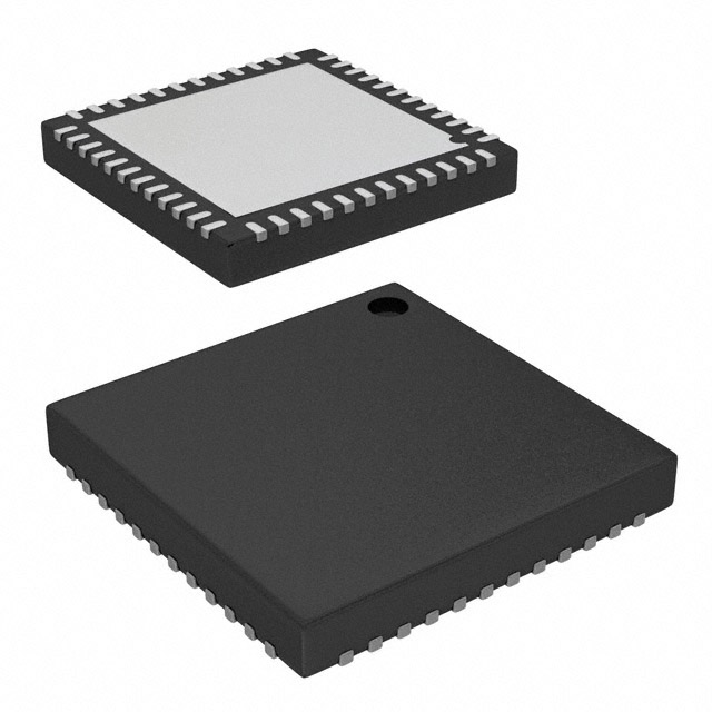


 工商网监
湘ICP备2023018690号
工商网监
湘ICP备2023018690号

