Atmel ATA664251
16K Flash Microcontroller with LIN Transceiver,
5V Regulator, Watchdog, 8-channel High Voltage Switch
Interface with High Voltage Current Sources, 16-bit SPI
DATASHEET
General Features
● Single-package high performance, low-power AVR® 8-bit microcontroller with
LIN transceiver, 5V regulator (80mA current capability), watchdog, 8-channel High
Voltage (HV) switch interface with High Voltage (HV) current sources and 16-bit
Serial Programming Interface (SPI)
● Very low current consumption in Sleep Mode
● 16-Kbytes flash memory for application program
● Supply voltage up to 40V
● Operating voltage: 5V to 27V
● Temperature range: Tcase –40°C to +125°C
● QFN48, 7mm × 7mm package
9269B–AUTO–11/12
�1.
Description
Atmel® ATA664251 is a System-in-Package (SiP) product, which is particularly suited for complete LIN-bus node applications. It
is especially designed for LIN-switch applications and includes nearly the complete LIN node. It consists of two ICs in one
package supporting highly integrated solutions for in-vehicle LIN networks. The first chip is the LIN-system-basis-chip (LINSBC) ATA664151, which has an integrated LIN transceiver, a 5V regulator (80mA), a window watchdog, an 8-channel High
Voltage Switch Interface with High Voltage Current Sources and a 16-bit SPI for configuration and diagnosis.
The second chip is an automotive microcontroller from the series of AVR® 8-bit microcontrollers from Atmel with advanced
RISC architecture, the Atmel ATtiny167 with 16-Kbytes flash memory.
All pins of the LIN-SBC as well as all pins of the AVR microcontroller are bonded out to provide customers the same flexibility for
their applications as they have when using discrete parts.
In Section 2. “Pin Configuration” on page 2 you will find the pin configuration for the complete SiP. The Section 4. “LIN-systembasis-chip (LIN-SBC) Block” on page 5 describes the LIN-SBC, and Section 5. “AVR Microcontroller Block” on page 44
describes the AVR microconroller.
Figure 1-1. Application Diagram
LIN-bus
Atmel ATA664251
MCU
Atmel
ATtiny 167
Pin Configuration
PA5
PA4
PA6
AGND
AVCC
PA3
PA0
PA2
PA1
PB0
PB1
PB2
Figure 2-1. Pinning QFN48
48 47 46 45 44 43 42 41 40 39 38 37
PA7
PB7
PB6
VDD
PB4
PB5
CS4
CS5
CS6
CS7
CS8
VS
1
36
35
2
34
3
4
5
6
33
Atmel
ATA664251
32
31
7
8
30
29
9
28
10
27
11
12
26
25
PB3
LIN
VBATT
CL15
CS3
CS2
CS1
IREF
VDIV
WDOSC
PWM3
PWM2
13 14 15 16 17 18 19 20 21 22 23 24
GND
VCC
NTRIG
TXD
RXD
NRES
NIRQ
MISO
MOSI
SCK
NCS
PWM1
2.
LIN-SBC
Atmel
ATA664151
Atmel ATA664251 [DATASHEET]
9269B–AUTO–11/12
2
�Table 2-1.
Pin Description
Pin
Symbol
Function
1
PA7
Port A 7 I/O line (PCINT7/ADC7/AIN1)
2
PB7
Port B 7 I/O line (PCINT15/ADC10/OC1BX / RESET)
3
PB6
Port B 6 I/O line (PCINT14/ADC9/OC1AX/INT0)
4
VDD
AVR supply voltage
5
PB4
Port B 4 I/O line (PCINT12/OC1AW/XTAL1/CLKI)
6
PB5
Port B 5 I/O line (PCINT13/ADC8/OC1BW/XTAL2/CLKO)
7
(1)
CS4
High-voltage current source and switch I/O-pin no. 4
8
CS5(1)
High-voltage current source and switch I/O-pin no. 5
9
(1)
High-voltage current source and switch I/O-pin no. 6
(1)
High-voltage current source and switch I/O-pin no. 7
(1)
High-voltage current source and switch I/O-pin no. 8
10
11
12
13
14
15
CS6
CS7
CS8
VS(1)
Supply input pin
(1)
System ground LIN-SBC
(1)
5V regulator output pin
GND
VCC
NTRIG
(1)
16
TXD(1)
17
(1)
18
LIN-bus logic data input
RXD
LIN-bus logic data output
(1)
Watchdog and VCC undervoltage Reset output pin (open drain, active low)
(1)
Interrupt request output to microcontroller (active low, open drain)
NRES
19
NIRQ
20
MISO(1)
21
(1)
22
23
Watchdog trigger input
MOSI
SPI Master-In-Slave-Out output pin to microcontroller
SPI Master-Out-Slave-In input pin from microcontroller
(1)
SPI clock input from microcontroller
(1)
SPI chip select logic input from microcontroller (active low)
SCK
NCS
24
PWM1(1)
25
(1)
PWM control input port from microcontroller for second CS pin group
(1)
PWM control input port from microcontroller for second CS pin group
26
PWM2
PWM3
(1)
PWM control input port from microcontroller for first CS pin group
27
WDOSC
28
VDIV(1)
29
(1)
Reference current adjustment pin
(1)
High-voltage current sink/source and switch I/O-pin no. 1
31
(1)
CS2
High-voltage current sink/source and switch I/O-pin no. 2
32
CS3(1)
High-voltage current sink/source and switch I/O-pin no. 3
30
33
IREF
CS1
CL15
(1)
(1)
Connection for external resistor to set watchdog frequency
Voltage divider output / Watchdog disable input pin
Wake-up on ignition high-voltage input pin
34
VBATT
35
(1)
Battery voltage input for voltage divider
LIN
LIN-bus line input/output
36
PB3
Port B 3 I/O line (PCINT11/OC1BV)
37
PB2
Port B 2 I/O line (PCINT10/OC1AV/USCK/SCL)
Atmel ATA664251 [DATASHEET]
9269B–AUTO–11/12
3
�Table 2-1.
Pin Description (Continued)
Pin
Symbol
38
PB1
Port B 1 I/O line (PCINT9/OC1BU/DO)
39
PB0
Port B 0 I/O line (PCINT8/OC1AU/DI/SDA)
40
PA1
Port A 1 I/O line (PCINT1/ADC1/TXD/TXLIN)
41
PA2
Port A 2 I/O line (PCINT2/ADC2/OC0A/DO/MISO)
42
PA0
Port A 0 I/O line (PCINT0/ADC0/RXD/RXLIN)
43
PA3
Port A 3 I/O line (PCINT3/ADC3/ISRC/INT0)
44
AVCC
Analog supply voltage
45
AGND
Analog ground
46
PA6
Port A 6 I/O line (PCINT6/ADC6/AIN0/SS)
47
PA4
Port A 4 I/O line (PCINT4/ADC4/ICP1/DI/SDA/MOSI)
48
PA5
Port A 5 I/O line (PCINT5/ADC5/T1/USCK/SCL)
Backside
Note:
3.
1.
Function
Heat slug is connected to GND
This identifies the pins of the LIN-SBC Atmel® ATA664151.
Absolute Maximum Ratings of the SIP
Stresses beyond those listed under “Absolute Maximum Ratings” may cause permanent damage to the device. This is a stress rating
only and functional operation of the device at these or any other conditions beyond those indicated in the operational sections of this
specification is not implied. Exposure to absolute maximum rating conditions for extended periods may affect device reliability.
Parameters
Symbol
HBM ESD
ANSI/ESD-STM5.1
JESD22-A114
AEC-Q100 (002)
Min.
Typ.
Max.
Unit
±3
KV
CDM ESD STM 5.3.1
±600
V
Machine Model ESD AEC-Q100-RevE
±200
V
Storage temperature
Ts
–55
+150
°C
Operating temperature(1)
Tcase
–40
+125
°C
Thermal resistance junction to heat slug
Rthjc
5
K/W
Thermal resistance junction to ambient
Rthja
25
K/W
Thermal shutdown of VCC regulator
150
165
170
°C
Thermal shutdown of LIN output
150
165
170
°C
Thermal shutdown hysteresis
Note:
10
°C
Tcase means the temperature of the heat slug (backside). It is mandatory that this backside temperature is ≤ 125°C in the
application.
Atmel ATA664251 [DATASHEET]
9269B–AUTO–11/12
4
�4.
LIN-system-basis-chip (LIN-SBC) Block
4.1
Features
●
●
●
●
●
●
●
●
●
●
●
8-channel HV switch interface with HV current sources
●
●
●
●
●
●
●
LIN High-speed Mode up to 200kBit/s
Linear low-drop voltage regulator, up to 80mA current capability, VCC = 5.0V ±2%
Fulfills the OEM “Hardware Requirements for LIN in Automotive Applications Rev.1.3”
LIN master and slave operation possible
Supply voltage up to 40V
Operating voltage VS = 5V to 27V
Internal voltage divider for VBattery sensing (±2%)
16-bit serial interface (daisy-chain-capable) for configuration and diagnosis
Typically 8µA supply current during Sleep Mode
Typically 35µA supply current in Active Low-power Mode
VCC-undervoltage detection (4ms reset time) and watchdog reset logical combined at open drain output NRES open
drain output
Adjustable watchdog timer via external resistor
Negative trigger input for watchdog
LIN physical layer complies with LIN 2.1 specification and SAE J2602-2
Wake-up capability via LIN bus and CL15
Bus pin is overtemperature and short-circuit protected versus GND and Battery
Advanced EMC and ESD performance
Atmel ATA664251 [DATASHEET]
9269B–AUTO–11/12
5
�4.2
Description
The LIN-SBC includes an eight-channel high voltage switch interface, a LIN 2.1 and SAEJ2602-2-compliant LIN transceiver,
low-drop voltage regulator, and an adjustable Window Watchdog. The voltage regulator has an output voltage of 5V and is able
to drive 80mA. This chip combination is especially designed for LIN switch applications. It is designed to handle low data-rate
communication in vehicles (such as in convenience electronics). Improved slope control at the LIN driver ensures secure data
communication up to 20kBaud. Sleep Mode and Active Low-power Mode guarantee minimal current consumption even in the
case of a floating bus line or a short circuit on the LIN bus to GND.
Figure 4-1. Block Diagram
RXD TXD
LIN
VS
NCS
SCK
MOSI
16-bit Serial
Programming
Interface
(SPI)
LIN Physical Layer
Interface
Internal
Supplies
Voltage
Regulator
VCC
MISO
CL15
VBATT
HV Input
NRES
VBATT
Voltage
Divider
Control Logic
NIRQ
Int. Oscillator
HV Switch
Interface
(8x)
Window Watchdog
WD-Oscillator
VDIV
PWM1
PWM2
PWM3
NTRIG
WDOSC AGND
GND
IREF CS1 CS2 CS3 CS4 CS5 CS6 CS7 CS8
Atmel ATA664251 [DATASHEET]
9269B–AUTO–11/12
6
�4.3
Pin and Functional Description
4.3.1
Physical Layer Compatibility
Since the LIN physical layer is independent of higher LIN layers (such as the LIN protocol layer), all nodes with a LIN physical
layer as per release version 2.1 can be mixed with LIN physical layer nodes found in older versions (i.e., LIN 1.0, LIN 1.1,
LIN 1.2, LIN 1.3, LIN 2.0), without any restrictions.
4.3.2
Supply Pin (VS)
The operating voltage is VS = 5V to 27V. An undervoltage detection is implemented to disable data transmission via the LIN bus
and the switch interface if VVS falls below VVSth in order to avoid false bus messages. After switching on VS, the IC starts in
Active Mode (see also the Section 4.4.1 “Active Mode” on page 11), with the VCC voltage regulator and the Window Watchdog
switched on (the latter depends on the VDIV pin, see Section 4.10 “Watchdog” on page 30).
4.3.3
Ground Pins GND and AGND
The IC is neutral on the LIN pin in the event of GND disconnection. It can handle a ground shift of up to 11.5% of VS.
Note:
4.3.4
Please note that pin AGND is used for internal reference generation. This should be considered when designing
the PCB in order to minimize the effect on the voltage thresholds.
Voltage Regulator Output Pin (VCC)
The internal 5V voltage regulator is capable of driving loads up to 80mA for supplying the microcontroller and other loads on the
PCB. It is protected against overloads by means of current limitation and overtemperature shutdown. In addition, the output
voltage is monitored and will cause a reset signal at the NRES output pin if it drops below a defined threshold VVCCthun.
A safe operating area (SOA) is defined for the voltage regulator, because the power dissipation caused by this block might
exceed the system’s thermal budget.
4.3.5
Bus Pin (LIN)
A low-side driver with internal current limitation, thermal shutdown and an internal pull-up resistor in compliance with the LIN 2.1
specification are implemented. The allowed voltage range is from –30V to +40V. Reverse currents from the LIN bus to VS are
suppressed, even in the event of GND shifts or battery disconnection. The LIN receiver thresholds are compatible with the LIN
protocol specification. The fall time from recessive to dominant bus state and the rise time from dominant to recessive bus state
are slope-controlled.
For higher bit rates the slope control can be switched off by setting the SPI-bit LSME. Then the slope time of the LIN falling edge
is < 2µs. The slope time of the rising edge strongly depends on the capacitive load and the pull-up resistance at the LIN-line. To
achieve a high bit rate it is recommended to use a small external pull-up resistor (500Ω) and a small capacitor. This allows very
fast data transmission up to 200kBit/s, e.g., for electronic control tests of the ECU, microcontroller programming or data
download. In this High-speed Mode a superior EMC performance is not guaranteed.
Note:
4.3.6
The internal pull-up resistor is only switched on in Active Mode and when the LIN transceiver is activated by the
LINE-Bit (Active Mode with LIN bus transceiver).
Bus Logic Level Input Pin (TXD)
The TXD pin is the microcontroller interface for controlling the state of the LIN output. TXD must be pulled to ground in order to
keep the LIN bus in the dominant state. If TXD is high or not connected (internal pull-up resistor), the LIN output transistor is
turned off and the bus is in recessive state.
If configured, an internal timer prevents the bus line from being constantly driven in the dominant state. If TXD is forced to low
for longer than tDOM, the LIN bus driver is switched back to recessive state. TXD has to be switched to high for at least tTOrel to
reactivate the LIN bus driver (by resetting the timeout timer).
As mentioned above, this timeout function can be disabled via the SPI configuration register in order to achieve any long
dominant state on the connected line (such as PWM transmission, or low bit rates).
Atmel ATA664251 [DATASHEET]
9269B–AUTO–11/12
7
�4.3.7
Bus Logic Level Output Pin (RXD)
This output pin reports the state of the LIN bus to the microcontroller. LIN high (recessive state) is reported by a high level,
LIN low (dominant state) is reported by a low level at RXD. The output has push-pull characteristics meaning no external time
defining measures are required. During states of disabled LIN-PHY (configuration bit “LINE” = 0), pin RXD is at high level.
Please note that the signal on the RXD pin is not valid for a certain period of time upon activation of the LIN transceiver
(tRXDinvalid).
Figure 4-2. RXD Timing upon Transceiver Enable
NCS
SPI word with LINE = 1
RXD
X
LIN bus state
0 = DOM --- 1 = REC
tRXDinvalid
RXD is switched off in Sleep- and Unpowered Mode.
4.3.8
CL15 Pin
The CL15 pin is a high-voltage input that can be used to wake up the device from Sleep Mode. It is an edge-sensitive pin (lowto-high transition). Thus, even if CL15 pin is at high voltage (VCL15 > VCL15th), it is possible to switch into Sleep Mode. It is usually
connected to the ignition for generating a local wake-up in the application if the ignition is switched on. The CL15 pin should be
tied directly to ground if not needed. A debounce timer with a value tdebCL15 of typically 160µs is implemented. The pin state
(CL15 ON or OFF) can be read out through the SPI interface.
4.3.9
Reset Output Pin (NRES)
The Reset Output pin is an open drain output and switches to low during a VCC undervoltage event or a watchdog timing
window failure. Please note the reset hold time of typically 4ms after the undervoltage condition has disappeared.
4.3.10 Interrupt Request Output Pin (NIRQ)
The interrupt request output pin is an open drain output and switches to low whenever a chip-internal event occurs that is set up
to trigger an interrupt. A power-up, a wake-up over LIN bus, a change in a switch state or an overtemperature condition are
examples of such events. The pin remains at ground until the end of the next SPI command, where the interrupt source is
passed to the SPI master (bits IRQS, see also Section 4.7 “Serial Programming Interface (SPI)” on page 19).
4.3.11 WDOSC Output Pin
The WDOSC output pin provides a typical voltage of 1.2V intended to supply an external resistor with values between 34K and
120K. The value of the resistor and with it the pin output current adjusts the watchdog oscillator frequency to provide a certain
range of time windows.
If the watchdog is disabled, the output voltage is switched off and the pin can either be tied to VCC or left open.
4.3.12 NTRIG Input Pin
The NTRIG input pin is the trigger input for the Window Watchdog. A pull-up resistor is implemented. A falling edge triggers the
watchdog. The trigger signal (low) must exceed a minimum time ttrigmin to generate a watchdog trigger and avoid false triggers
caused by transients. The NTRIG pin should be tied directly to VCC if not needed.
4.3.13 VBATT Input Pin
The VBATT is a high voltage input pin for measurement purposes by means of a voltage divider. The latter provides a lowvoltage signal at the VDIV pin that is linearly dependent on the input voltage. In an application with battery voltage monitoring,
this pin is connected to VBattery via a 51Ω resistor in series and a 10nF capacitor to GND. The divider ratio is 1:4, resulting in a
maximum output voltage on pin VDIV when reaching 20V at the input. The VBATT pin can be tied directly to ground or left open
if not needed
Atmel ATA664251 [DATASHEET]
9269B–AUTO–11/12
8
�4.3.14 VDIV Input/Output Pin
This pin handles two different functions. During the VCC startup and watchdog reset phase (pin NRES driven to LOW), the pin
act as input and determines the setting of the “WDD” bit within the SPI configuration register (see Figure 4-3). In other words, if
the Window Watchdog operation shall be disabled directly after power-up (e.g., for µC programming or debugging purposes),
pin VDIV must be tied to the HIGH level until the reset phase ends (pin NRES has a positive slope from LOW to HIGH). In other
cases, such as when pin VDIV is not driven actively by the application, the signal is assessed as LOW and the WDD bit
(watchdog disable) is thus also low and the Window Watchdog is operational (see Figure 4-3).
Figure 4-3. WDD Configuration Bit Setup During VCC Startup
NRES
“LOW” from VCC startup
VDIV (driven externally)
WDD config bit state
Logic Level “A”
X
Z (high imp.)
Logic Level “A”
During normal operation this pin provides a low-voltage signal for the ADC such as for a microcontroller. It is sourced either by
the VBATT pin or one of the switch input pins CS1 to CS8. An external ceramic capacitor is recommended for low-pass filtering
of this signal. If selected in the configuration register of the SPI, this pin guarantees a voltage- and temperature-stable output
ratio of the selected test input and is available in all modes except Sleep Mode. Please note that the current consumption values
in the Active Low-power Mode of Atmel LIN-SBC given in the electrical characteristics lose their validity if the VDIV output pin is
being used in this Low-power Mode. The voltage on this pin is actively clamped to VCC if the input value would lead to higher
values.
4.3.15 IREF Output Pin
This pin is the connection for an external resistor towards ground. It provides a regulated voltage which will cause a resistordependnt current used as reference for the current sources in the switch interface I/O ports. The resistor should be placed
closely to the pin without any additional capacitor. A fail-safe circuitry detects if the resistor is missing or if there is a short
towards ground or VCC on this pin. An internal fail-safe current is generated in this event. Please see also Section 4.8 “Switch
Interface Unit” on page 24 for further details.
4.3.16 CS1 to CS8 High-voltage Input/Output Pins
These pins are intended for contact monitoring and/or constant current sourcing. A total of eight I/Os (pins CS1 through CS8)
are available, of which three (CS1, CS2 and CS3) can be configured either as current sources (such as for switches towards
ground) or as current sinks (such as for switches towards battery). The other five pins (CS4 to CS8) have only current sourcing
capability. Apart from a high voltage (HV) comparator for simple switches, the I/Os are also equipped with a voltage divider to
enable analog voltage measurements on HV pins by using the ADC of the application’s microcontroller (see Section 4.3.14
“VDIV Input/Output Pin” on page 9 for further details). Also, each input can trigger an interrupt upon state change even during
Active Low-power Mode. If one or more CSx pins are not needed, can be left open or directly connected to VS.
Note:
Unused CSx-pins should be connected directly to VS.
4.3.17 PWM1..3 Input Pins
These pins can be used to control the switch interface current sources directly, such as for pulse width-modulated load control
or for pulsed switch scanning. They accept logic level signals from the microcontroller and are equipped with pull-down
structures so in case of an open connection, the input is well defined. For more information see Section 4.8 “Switch Interface
Unit” on page 24.
The assignment of the current sources to the three PWM input pins is described in Section 4.8.1 “Current Sources” on page 24.
Atmel ATA664251 [DATASHEET]
9269B–AUTO–11/12
9
�4.4
Operating Modes
There are two primary modes of operation available.
● Active Mode:
In this mode the VCC voltage regulator is active and the SPI is ready for operation. In addition, all other peripherals can
be enabled or disabled by configuration via SPI. After power-up the watchdog is enabled (dependnt on the VDIV pin only,
see Section 4.3.14 “VDIV Input/Output Pin” on page 9), whereas the LIN transceiver and the Switch Interface Unit are
switched off.
●
Sleep Mode:
All peripherals are switched off (including the VCC voltage regulator), a wake-up is only possible via the LIN bus or the
CL15 pin. In this mode the IC has the lowest possible current consumption.
Figure 4-4. State Diagram
Unpowered Mode
All circuitry OFF
VVS < 3.3V
VVS > 3.5V
Config Init
Load WDD bit dependent
on VDIV input level
Active Mode
VVS < 3.3V
VCC: ON
All other peripherals
config dependent
SLEEP bit = 1
LIN Wake up or
CL15 Wake up
Sleep Mode
VCC: OFF
All other peripherals:
OFF
VVS < 3.3V
Atmel ATA664251 [DATASHEET]
9269B–AUTO–11/12
10
�4.4.1
Active Mode
If sufficient voltage is applied to the IC at the VS pin, the configuration register is initialized and the chip changes to Active
Mode. In this mode different states of power consumption are possible, depending on the configuration selected for the chip and
activity on the SPI. The following table lists all power states (except unpowered) for the LIN-SBC.
Table 4-1.
State and Current Consumption vs. Enabled Periphery
State and VS Pin
Current
Consumption
Sleep
IVS = IVSsleep
LIN-bus
Transceiver
Voltage
Divider
VCC Voltage
Regulator
Watchdog
SPI Data
Comm.
Current
Sources
Off
Off
Off
Off
Off
Off
Active Low-power
Off
Off
IVS = IVSact_lp
(LINE=0)
(VDIVE=0)
Active SPI Comm.
Off
Off
IVS = IVSact_spi
(LINE=0)
(VDIVE=0)
Active with watchdog
Off
Off
IVS = IVSact_wd
(LINE=0)
(VDIVE=0)
Active with LIN-bus
transceiver
On
Off
(LINE=1)
(VDIVE=0)
IVS = IVSact_lin
On
On
On
On
Off or
Standby
Off
Off
(WDD=1)
(NCS=1)
(CSEx=X and
CSCx=0 and
PWMy=0)
Off
On
Off
(WDD=1)
(NCS=0)
(CSEx=0)
On
(WDD=0)
Off
(WDD=1)
do not care
do not care
Off
(CSEx=0)
Off
(CSEx=0)
On
Active with Current
Sources
IVS = IVSact_cs
Active with Voltage
Divider
IVS = Iact_vdiv
Note:
Off
Off
(LINE=0)
(VDIVE=0)
Off
On
(LINE=0)
(VDIVE=1)
On
On
Off
(WDD=1)
Off
(WDD=1)
do not care
do not care
(CSEx=1 and
(CSCx=1 or
PWMy=1))
Off
(CSEx=0)
Legend:
0 = bit is programmed 0
1 = bit is programmed 1,
X = Disregards
The descriptions in brackets below the peripherals refer to the configuration register, accessible via SPI.
Please note that the table above only lists the Active Mode states with just one extra peripheral enabled. Except for Active Lowpower, any combination of the states above and thus also the current consumption is possible - for example, the parallel
operation of the LIN bus transceiver and the current sources. The required supply current is then at least the sum of the values
given above.
Atmel ATA664251 [DATASHEET]
9269B–AUTO–11/12
11
�4.4.2
Sleep Mode
This mode must be initialized via the SPI configuration register. All peripherals, i.e., the LIN transceiver, the watchdog, the
voltage dividers, the Switch Interface Unit and the VCC voltage regulator are switched off. The overall supply current on pin VS
is then reduced to a minimum.
Two wake-up mechanisms are possible to leave Sleep Mode again: wake-up via LIN and wake-up via CL15.
4.4.2.1 Wake-up from Sleep Mode via LIN
A voltage below the LIN Pre-Wake threshold on the LIN pin activates a wake-up detection phase.
A falling edge at the LIN pin followed by a dominant bus level maintained for a time period of at least tbus and the following
rising edge at the LIN pin (see Figure 4-5) results in a remote wake-up request. The device switches from Sleep Mode to Activelow Power Mode (VCC regulator enabled), but the LIN transceiver is still deactivated. Only the internal LIN slave termination
resistor is switched on. The remote wake-up request is indicated by a low level at the NIRQ pin to interrupt the microcontroller
(see Figure 4-5). In addition, the wake-up source is stated in the chip status register which can be read out via SPI. Configuring
the chip via SPI must be used to enable the LIN transceiver and allow data to be send and/or transmited data via the LIN bus.
Note that this can only be done after the LOW level at the NRES pin has been elinimated (after VCC ramp-up and the
stabilization phase).
Figure 4-5. LIN Wake-up from Sleep Mode
LIN Bus
VCC
NRES
NIRQ
SPI Comm.
Watchdog State
Init IC/ Read Status
Watchdog off
tbus = 90μs typ
VCC
Startup
Start Watchdog Lead Time
tnres = 4ms typ
With the initialization of the configuration register by the microcontroller, the status word of the LIN-SBC is transmitted back,
including the wake-up source. In other words, the two status bits “IRQS1” and “IRQS0” both read back as ‘1’. For more
information see Section 4.7 “Serial Programming Interface (SPI)” on page 19.
Atmel ATA664251 [DATASHEET]
9269B–AUTO–11/12
12
�4.4.2.2 Wake-up from Sleep Mode via CL15
Voltage above VCL15H at pin CL15 activates a CL15 wake-up detection phase. This state must persist for at least tCLdeb in order
to detect a wake-up. If the pulse is too short, the IC remains in Sleep Mode.
When leaving Sleep Mode first the VCC voltage regulator is activated to enable the microcontroller supply. Then as soon as the
VCC level reaches valid levels, the VCC startup timer is started. During this time, the NRES pin is kept low in order to keep the
microcontroller from running. This ensures a proper voltage supply and signal stabilization in the application. With the rising
edge at NRES, the SPI is ready for communication and the LIN-SBC can be initialized.
Figure 4-6. CL15 Wake-up from Sleep Mode
CL15
VCC
NRES
NIRQ
SPI Comm.
Watchdog State
Init IC/ Read Status
Watchdog off
tCL15deb = 160μs typ
VCC
Startup
Start Watchdog Lead Time
tnres = 4ms typ
The wake-up behavior is analogous to a wake-up via the LIN bus as seen above. One difference is that no negative edge is
required to start the wake-up procedure as is the case for LIN wake-ups. After the VCC startup time tWDnres has elapsed, NRES
is released and therefore pulled up, either by the internal or additional external resistors. The microcontroller can then configure
the LIN-SBC and thus be notified about the actual status including the wake-up source. Here, the two status bits “IRQS1” and
“IRQS0” read back as ‘10’.
Atmel ATA664251 [DATASHEET]
9269B–AUTO–11/12
13
�4.4.2.3 Sleep Mode: Behavior at a Floating LIN bus or a Short-circuited LIN to GND
In Sleep Mode the device has very low current consumption even during short-circuits or floating conditions on the bus. A
floating bus can arise if the master pull-up resistor is missing, such as when it is switched off while the LIN master is in Sleep
Mode or even if the power supply of the master node is switched off.
In order to minimize the current consumption IVS in Sleep Mode during voltage levels on the LIN pin below the LIN Pre-wake
threshold, the receiver is activated only for a specific time tmon. If tmon elapses while the voltage at the bus is lower than Prewake detection low (VLINL) or higher than the LIN dominant level, the receiver is switched off again and the circuit changes back
to Sleep Mode. The current consumption is then IVSsleep_short (typ. 10µA more than IVSsleep). If a dominant state is reached on the
bus, no wake-up occurs. Even if the voltage rises above the Pre-wake detection high (VLINH), the IC will stay in Sleep Mode.
This means the LIN bus must be above the Pre-wake detection threshold VLINH for a few microseconds before a new LIN wakeup is possible.
Figure 4-7. Floating LIN Bus During Sleep Mode
LIN Pre-wake
VLINL
LIN BUS
LIN dominant state
VBUSdom
tmon
IVSsleep_short
IVSfail
IVS
IVSsleep
Mode of
operation
Int. Pull-up
Resistor
RLIN
Sleep Mode
IVSsleep
Wake-up Detection Phase
Sleep Mode
off (disabled)
If the LIN-SBC is in Sleep Mode and the voltage level at the LIN bus is in dominant state (VLIN < VBUSdom) for a period exceeding
tmon (during a short circuit at LIN, for example), the IC switches back to Sleep Mode. The VS current consumption is then
IVSsleep_short (typ. 10µA more than IVSsleep). After a positive edge at the LIN pin the IC switches directly to Active Mode.
Atmel ATA664251 [DATASHEET]
9269B–AUTO–11/12
14
�Figure 4-8. Short Circuit to GND on the LIN Bus During Sleep Mode
LIN Pre-wake
LIN BUS
VLINL
LIN dominant state
VBUSdom
tmon
tmon
IVSsleep_short
IVSfail
IVS
Mode of
operation
IVSsleep
Sleep Mode
Int. Pull-up
Resistor
RLIN
4.4.3
Wake-up Detection Phase
off (disabled)
Sleep Mode
Active Mode
on (enabled)
Active Low-power Mode
In this mode, the VCC voltage regulator is active and can therefore supply the application’s microcontroller.
All other functions of the LIN-SBC are disabled in the configuration register respectively inhibited by the PWM pins for the CSx
pin current sources. This reduces the current consumption of the chip itself to a low-power range of typically below 50µA. Note
that this is only valid if the chip select input of the SPI, NCS, is also kept at a high level. If it is pulled to ground, SPI
communication is enabled, causing a higher current consumption.
If the LIN transceiver is disabled, the bus is monitored for a wake-up event, initialized with a voltage level below the LIN Prewake threshold at the LIN pin.
Atmel ATA664251 [DATASHEET]
9269B–AUTO–11/12
15
�Figure 4-9. LIN Wake-up from Active Low-power Mode
LIN Bus
VCC
NRES
NIRQ
SPI Comm.
Enable WD/ Read Status
Watchdog State
Watchdog off
Start Watchdog Lead Time
tbus = 90μs typ
The negative edge on the NIRQ pin indicates a change of conditions, in this case a wake-up request at the LIN bus. The
microcontroller can check the IRQ source by assessing the “IRQS1” and “IRQS0” bits in the status register. Note that if a
watchdog operation is desired, it must be enabled via the configuration register.
The behavior can be transferred to a wake-up over CL15 pin from Active Low-power Mode.
Figure 4-10. CL15 Wake-up from Active Low-power Mode
CL15
VCC
NRES
NIRQ
SPI Comm.
Watchdog State
Enable WD/ Read Status
Watchdog off
Start Watchdog Lead Time
tCL15deb = 160μs typ
Apart from the LIN transceiver and the CL15 input, the high-voltage I/O ports CS1 to CS8 can also be used to generate
interrupts while in Active Low-power Mode. This can be done by enabling the current sources so that they can generate an
interrupt with the corresponding CSEx- and CSIEx bits in the configuration register. As long as the current source is not enabled
(CSCx=’0’ and PWMy low), the IC stays in Active Low-power Mode (if all other conditions are met, such as disabled watchdog).
The PWMy pin has to be set to high by the microcontroller, for example, controlled via a PWM timer unit, in order to check the
condition of the connected switch. Because the switch interface unit is enabled, current consumption increases drastically. This
“switch scanning phase” can be short compared to the interceding idle time so the mean current consumption of the IC remains
close to the Active Low-power Mode current consumption. For more information , see Section 4.8.1 “Current Sources” on page
24 and Section 4.8.2 “Switch Inputs” on page 26 for further details.
Atmel ATA664251 [DATASHEET]
9269B–AUTO–11/12
16
�4.4.4
Behavior under Low Supply Voltage Conditions
When connected to the car battery, the voltage at the VS pin increases according to the blocking capacitor (see Figure 4-11). As
soon as VVS exceeds its undervoltage threshold VVSthO, the Switch Interface Unit and the LIN transceiver can be used. The LINSBC is in Active Mode after power-up with the VCC voltage regulator and the Window Watchdog enabled – the latter depends
on the state of the pin VDIV. The VCC output voltage reaches its nominal value after tVCC. This time depends on the externally
applied VCC capacitor and the load.
The NRES is low for the reset time delay treset. During this time treset, no SPI communication and thus no configuration changes
or status checks are possible.
Figure 4-11. VCC versus VS
7.0
6.5
6.0
5.5
5.0
Regulator drop voltage VD
4.5
V in V
4.0
LIN
3.5
3.0
2.5
VS
2.0
NRES
1.5
VCC
1.0
0.5
0
0
0.5
1.0
1.5
2.0
2.5
3.0
3.5
4.0
4.5
5.0
5.5
6.0
6.5
7.0
VS in V
Please note that upper graph is only valid if the VS ramp-up time is much slower than the VCC ramp-up time tVCC and the NRES
delay time treset.
If during Active Mode the voltage level of VS drops below the undervoltage detection threshold VVSthU, an interrupt is indicated
to the microcontroller by means of a low-signal at the NIRQ pin. Furthermore, both the Switch Interface Unit and the LIN
transceiver are shut down in order to avoid malfunctions or false bus messages. This shutdown is achieved by simply inhibiting
the functions internally. The corresponding bits in the configuration register are not cleared. This means the functionality
resumes if enabled after the supply voltage exceeds above VVSthO again.
If during Sleep Mode the voltage level of VS drops below the undervoltage detection threshold VVSthU, no change of mode or
any other activity by the LIN-SBC occurs as long as the level does not drop below the minimum operation value VVSopmin.
4.5
Wake-up Scenarios from Sleep Mode
4.5.1
Remote Wake-up via the LIN Bus
A voltage lower than the LIN Pre-wake detection VLINL at the LIN pin activates the internal LIN receiver.
A falling edge at the LIN pin followed by a dominant bus level VBUSdom of at least tBUS and a rising edge at pin LIN results in a
remote wake-up request. The device switches from Sleep Mode to Active Mode. The VCC voltage regulator is activated and the
internal slave termination resistor is switched on. The remote wake-up request is indicated by a low level at the NIRQ pin. this
generates an interrupt for the microcontroller and a corresponding flag in the SPI register.
Atmel ATA664251 [DATASHEET]
9269B–AUTO–11/12
17
�4.5.2
Local Wake-up via Pin CL15
A positive edge at pin CL15 followed by a high voltage level for a given time period (> tCL15deb) results in a local wake-up
request. The device switches to Active Mode. The debouncing time ensures that no transients at CL15 create a wake-up. The
local wake-up request is indicated by a low level at the NIRQ pin, generating an interrupt for the microcontroller. During highlevel voltage at the CL15 pin, it is possible to switch to Sleep Mode via an SPI command. In this case the voltage at the CL15
pin has to be switched to low for at least tCL15deb before the positive edge at this pin starts a new local wake-up request. Note
that this time can be extended by adapting the external circuitry.
4.5.3
Wake-up Source Recognition
The device can distinguish between different wake-up sources.
The source for the wake-up event can be read out of the SPI diagnosis register.
4.6
Wake-up Scenarios from Active Low-power Mode
Generally the Active Low-power Mode is only possible if all clock-dependent peripherals such as the LIN transceiver and the
watchdog are disabled. In addition, no SPI communication is allowed to take place to minimize current consumption.
4.6.1
Wake-up from CSx Pins
The switch input pins can each be used to generate an interrupt request while in active low-power mode. A state change
detection circuitry is implemented for this functionality (see section Section 4.8.2 “Switch Inputs” on page 26). For this
functionality, the respective current source needs to be configured so that it is controlled via the dedicated PWMy pin. A rising
edge on this pin enables the current source, allowing a stable switch readback signal to be delivered at the CSx pin. The switch
state is updated with a falling edge at the PWMy pin. If a change of state is monitored, an interrupt request is generated if the
CSIE bit of the affected current source is set to '1' in the configuration register. If no wake-up should occur on a certain switch either because there is no application demand for this or a failure such as a hanging switch or a connection line short-circuit is
present - it can be prevented by disabling the current source in the SPI configuration register.
4.6.2
Wake-up from LIN Bus
If during Active Low-power Mode (i.e., the LIN transceiver is disabled) the LIN bus is tied to ground for at least tbus. This wakeup request is indicated by a negative edge at the NIRQ pin. Please note that the Atmel LIN-SBC stays in active Low-power
Mode for as long as no SPI communication occurs or configuration changes are made. Current consumption is only higher
during the LIN bus assessment, in other words as long as the voltage on the LIN bus is below VLIN,preL. Regardless of the
LIN bus state, this assessment phase ends after tLIN_wudet at the latest. This ensures a low current consumption even during
shorts on the LIN bus or when there are floating bus levels.
4.6.3
Wake-up from CL15
If during Active Low-power Mode the voltage on the CL15 pin exceeds VCL15H for at least tCL15deb, an interrupt request is
triggered to indicate a change of state at the CL15 pin. Please note that after the tCL15deb has elapsed, the LIN-SBC stays in
Active Low-power Mode for as long as no SPI communication occurs or configuration changes are made.
4.6.4
Wake-up from SPI
If during Active Low-power Mode the chip select input NCS is tied to ground, the LIN-SBC leaves the Active Low-power Mode in
order to complete a data communication with the SPI master. The operating mode of the IC is adapted in accordance with the
configuration register update. If no change in configuration has taken place – for example, because only the actual status was
polled or another bus member connected via daisy chaining was addressed – the LIN-SBC goes back to Active Low-power
Mode as soon as NCS returns to High level.
Atmel ATA664251 [DATASHEET]
9269B–AUTO–11/12
18
�4.7
Serial Programming Interface (SPI)
Most features of the LIN-SBC are configured via SPI. Diagnostics are carried out using this interface also. It can be used in
Active Mode as long as there is no undervoltage condition at the VCC pin.
The SPI features both POL = 0 / PHA = 0 and POL = 1 / PHA = 1 operating modes.
Figure 4-12. POL = 0 / PHA = 0 Setup
Sample
NCS
MOSI
Setup
X
MSB
14
13
12
2
1
LSB
X
X
Z
MSB
14
13
12
2
1
LSB
MOSI
MSB
Z
SCK
MISO
Figure 4-13. POL = 1 / PHA = 1 Setup
Setup
NCS
MOSI
Sample
X
X
Z
X
MSB
14
13
3
2
1
LSB
X
14
13
3
2
1
LSB
X
SCK
MISO
MSB
The interface contains four pins.
● NCS (chip select pin, active low)
●
●
●
SCK (serial data clock)
MOSI (Master-Out-Slave-In serial data port input from master)
MISO (Master-In-Slave-Out serial data port output from SBC; this pin is tri-state if NCS is high)
No data is loaded from MOSI on SCK edges or provided at MISO if chip select is not active. The output pin MISO is not actively
driven (tri-state) during these phases.
Atmel ATA664251 [DATASHEET]
9269B–AUTO–11/12
19
�The data transfer scheme (bit order) is MSB first, meaning the first bit that is transferred is the most significant bit of the register,
with the transfer ending with the least significant bit. These bits are listed on the next pages. The MOSI bits 15 to 0 refer to the
configuration register. This means the configuration register is updated with each SPI communication. At the same time the
MISO word is built from the status register bits 15 to 0. Note that changes in the configuration are only visible in the next status
query. This means,for example, that if you enable the watchdog with an SPI command, the status “Watchdog Active” is not
reported in this data transmission but in the next one.
In order to load any data into the chip, the chip select signal must be removed (i.e., set to high) after the 16 SCK clock periods.
A minimum data evaluation time tSPIeval,min has to transpire before the next data transfer can start. Please note also that any
change in configuration of the IC requires this time to go into effect.
Figure 4-14. SPI Configuration Timing
NCS
MOSI Data
Chip Configuration
Config Data
New Config
Previous Config
tSPIeval_min
The following table lists the bits of the configuration register in the LIN-SBC.
Table 4-2.
SPI ConfIguration Register
Bit Name
Description
Default (`0´)
Programmed
with `1´
15
MSB
LSME
Enable LIN-bus
High-Speed Mode
Normal
HighSpeed
See Section 4.3.5 “Bus Pin
(LIN)” on page 7
14
TTTD
Disable TxD Timeout
Timer
Enabled
Disabled
See Section 4.3.6 “Bus Logic
Level Input Pin (TXD)” on page 7
13
IMUL
IREF Multiplier Value
x100
x50
See section Section 4.8 “Switch
Interface Unit” on page 24
12
LINE
Enable LIN transceiver
Disabled
Enabled
See Section 4.3.5 “Bus Pin
(LIN)” on page 7
11
SLEEP
Go to Sleep
Stay in Active
Mode
Enable Sleep
Mode
See Section 4.4 “Operating
Modes” on page 10
10
VDIVE
Enable VDIV as output
VDIV off
(high-ohmic)
VDIV on (selected
voltage divider
active)
See Section 4.8.2.2 on page 28
and Section 4.8 “Switch
Interface Unit” on page 24
9
VDIVP
Programming VDIV
output source
VDIV shows
VBATT divider
VDIV shows one
CS divider output
See Section 4.8.2.2 on page 28
and Section 4.8 “Switch
Interface Unit” on page 24
8
CSPE
Enable Switch Interface
Disabled
Unit programming
Enabled
See Section 4.8 “Switch
Interface Unit” on page 24
#
Remark
Atmel ATA664251 [DATASHEET]
9269B–AUTO–11/12
20
�Table 4-2.
SPI ConfIguration Register (Continued)
Default (`0´)
Programmed
with `1´
#
Bit Name
Description
7
CSA2
Address bit 2 (MSB) for
0
Switch Input
1
Used as selector for VDIV
and for Programming of one
Current Source
6
CSA1
Address bit 1 for Switch
0
Input
1
Used as selector for VDIV
and for Programming of one
Current Source
5
CSA0
Address bit 0 (LSB) for
Switch Input
0
1
Used as selector for VDIV
and for Programming of one
Current Source
4
CSE
Enable addressed
current source
Disabled
Enabled
See Section 4.8 “Switch
Interface Unit” on page 24
3
CSSSM
Switch between
Source/Sink Mode
Source Mode
selected
(HighSide)
Sink Mode
Sink mode is only possible for
selected (LowSide) Switch Interfaces 1-3
2
CSC
Control of addressed
current source
External (CSE
and PWMy)
Internal
(CSE only)
See Section 4.8 “Switch
Interface Unit” on page 24
CSIE
(CSPE=1)
Enable Interrupt
from addressed Switch
Input
Enabled
CSIE will be altered if CSPE
of the SPI word is ‘1’.
See Section 4.8 “Switch
Interface Unit” on page 24
CSSCD
(CSPE=0)
CS port current source
slope control
Enabled
Disabled
CSSCD will be altered if CSPE
of the SPI word is ‘0’.
See Section 4.8 “Switch
Interface Unit” on page 24
WDD
Disable watchdog
Enabled
(if pin VDIV
on low level)
Disabled
See Section 4.10 “Watchdog” on
page 30
Disabled
1
0
LSB
Remark
Atmel ATA664251 [DATASHEET]
9269B–AUTO–11/12
21
�The following table lists the bits of the status register in the LIN-SBC.
Table 4-3.
#
SPI Status Register
Bit Name
Description
Result = "0"
Result = "1"
Remark
OTVCC
(VDIVE=0)
Overtemperature
prewarning from VCC
regulator temp sensor
Temperature
not critical
Temperature
critical
See Section 4.9 on page 29;
only valid if VDIVE of prev.
command was ‘0’
MVBATT
(VDIVE=1)
VBATT voltage monitor
VBATT not
visible on
VDIV
VBATT visible
on VDIV
Only valid if VDIVE of prev.
command was ‘1’
OTLIN
(VDIVE=0)
Overtemperature signal
from LIN driver temp sensor
no Overtemperature
Overtemperature
See Section 4.3.5 on page 7;
only valid if VDIVE of prev.
command was ‘0’
MRDIV2
(VDIVE=1)
CS port voltage monitor,
address bit 2 (MSB)
MRDIV2..0 indicate the address
of the CS port volt. monitor
visible on VDIV
This bit is only shown if VDIVE
of previous command was ‘1’
OTCS
(VDIVE=0)
Overtemperature signal
from current sources temp
sensor
no Overtemperature
See Section 4.8 on page 24;
only valid if VDIVE of prev.
command was ‘0’
MRDIV1
(VDIVE=1)
CS port voltage monitor,
address bit 1
MRDIV2..0 indicate the address
of the CS port volt. monitor
visible on VDIV
This bit is only shown if VDIVE
of previous command was ‘1’
CL15S
(VDIVE=0)
CL15 pin status
VCL15 <
VCL15H
See Section 4.12 on page 32;
only valid if VDIVE of prev.
command was ‘0’
MRDIV0
(VDIVE=1)
CS port voltage monitor,
address bit 0 (LSB)
MRDIV2..0 indicate the address
of the CS port volt. monitor
visible on VDIV
This bit is only shown if VDIVE
of previous command was ‘1’
11
WDS
Watchdog status
Watchdog
disabled
Watchdog
enabled
See Section 4.10 “Watchdog”
on page 30
10
VSS
VS voltage level status
VS voltage
OK
VS
undervoltage
See Section 4.4.4 on page 17
9
IRQS1
15
MSB
14
13
12
Interrupt request source
"00"
"01"
"10"
"11"
Overtemperature
VCL15 ≥ VCL15H
PowerUp
CS change
CL15 wake-up
LIN wake-up
Information will be cleared after
status register readout via SPI
8
IRQS0
7
CS8CS
Switch Interface 8
comparator status
VCS8 < VCSxth
VCS8 > VCSxth
See Section 4.8 “Switch
Interface Unit” on page 24
6
CS7CS
Switch Interface 7
comparator status
VCS7 < VCSxth
VCS7 > VCSxth
See Section 4.8 “Switch
Interface Unit” on page 24
5
CS6CS
Switch Interface 6
comparator status
VCS6 < VCSxth
VCS6 > VCSxth
See Section 4.8 “Switch
Interface Unit” on page 24
Atmel ATA664251 [DATASHEET]
9269B–AUTO–11/12
22
�Table 4-3.
SPI Status Register (Continued)
#
Bit Name
Description
Result = "0"
Result = "1"
Remark
4
CS5CS
Switch Interface 5
comparator status
VCS5 < VCSxth
VCS5 > VCSxth
See Section 4.8 “Switch
Interface Unit” on page 24
3
CS4CS
Switch Interface 4
comparator status
VCS4 < VCSxth
VCS4 > VCSxth
See Section 4.8 “Switch
Interface Unit” on page 24
2
CS3CS
Switch Interface 3
comparator status
VCS3 < VCSxth
VCS3 > VCSxth
See Section 4.8 “Switch
Interface Unit” on page 24
1
CS2CS
Switch Interface 2
comparator status
VCS2 < VCSxth
VCS2 > VCSxth
See Section 4.8 “Switch
Interface Unit” on page 24
0
LSB
CS1CS
Switch Interface 1
comparator status
VCS1 < VCSxth
VCS1 > VCSxth
See Section 4.8 “Switch
Interface Unit” on page 24
The SPI is capable of daisy chaining as well. In other words, if other ICs with a daisy-chaining-enabled SPI are to be used in the
application, they can simply be interconnected one after the other (see Figure 4-15).
Figure 4-15. Daisy Chaining Configuration
Microcontroller
NCS
NCS
SCK
SCK
MOSI
MOSI
MISO
MISO
NCS
SCK
MOSI
LIN-SBC
Other
SPI
Member
MISO
It can be seen that the data output of the LIN-SBC is not connected to the data input of the master but of another SPI member
which is also capable of daisy chaining. In order to transmit data, the microcontroller has to send the sum of clock pulses for all
bus members. In the example above, if the other SPI member also features 16 bits, the microcontroller has to perform 32 clock
cycles with NCS kept low to completely move the data. The first 16 bits of such a transmission are initially fed into the LIN-SBC.
But when NCS stays low, the data is not loaded into its configuration register but instead shifted out again with the next 16 bits.
At the same time the status register is first fed into the other SPI bus member which then needs to transfer the data over to the
microcontroller with the second 16 bits.
In summary, the daisy chaining is one way to have multiple bus members connected to a single master. Because not all devices
support these operation modes, the LIN-SBC still supports the direct addressing mode using the NCS pin. If NCS is not pulled
to ground, all data traffic on the SPI is disregarded by the LIN-SBC.
Atmel ATA664251 [DATASHEET]
9269B–AUTO–11/12
23
�4.8
Switch Interface Unit
A total of eight high-side current sources with high voltage comparators and voltage dividers are available for switch scanning or
for example, LED driving purposes. Note that three of them (CS1, CS2, and CS3) can also be switched to low-side current sinks
in the configuration register via the SPI. System wake-up from Active Low-power Mode is possible through state change
monitoring. Please see Figure 4-16 for an overview of the interface structure.
Figure 4-16. Principle Schematic of a High-Side-Only Switch Interface (CS4 - CS5)
VS
CSE [1..8]
IIREF × rlCS
PWMy
CSC [1..8]
State
change
detector
d_statechange
VCSxth (4V DC)
HV
comp
MUX
CSx
dout_cs_x
CSA [2..0]
VBATT
3R
VDIV
VDIVP
R
AGND
VDIVE
The control signals CSE and CSC are configuration register bits, and unique for each of the eight interfaces. The output signal
dout_cs of the comparator can be probed via the SPI status register bit CSxCS.
4.8.1
Current Sources
The current sources are available in Active Mode. They deliver a current level derived from a reference value measured at the
IREF pin. This pin is voltage-stabilized (VIREF = 1.23V typ.) so that the reference current is directly dependent on the externally
applied resistor connected between IREF pin and ground. The resulting current at the CSx- pins is (1.23V/RIref) x rICS. For
example, with a 12K resistor between IREF and GND the value of the current at the CSx-pins is 10mA (assumed
IMUL = '0' => rICS_H = 100). For fail-safe reasons, both a missing and a short-circuited resistor are detected. In this case, an
internally generated reference current IIREFfs is used instead to maintain a certain degree of functionality.
The current sources of I/Os 1-3 (CS1..CS3) can be configured either as High-sides (current sources) or Low-sides (current
sinks). This selection is done by the CSSSM bit of the configuration register. The default value of '0' enables the High-side
source whereas a '1' enables the Low-side sink.
The output current level can be divided by 2 with the IMUL bit in the configuration register. With the default setting of IMUL = '0',
the ratio between the output current ICSx and the reference current IIREF is rICS_H (typ. 100). If set to '1', the ratio reduces to rICS_L
(typ. 50).
Atmel ATA664251 [DATASHEET]
9269B–AUTO–11/12
24
�If a current source is enabled by the configuration register (set to ready state, bit CSE = '1'), it supports two different operating
modes.
● Directly controlled by the configuration register - bit CSC = '1'
●
Externally gated (inhibited with the PWMy pin) - bit CSC = '0' (default)
These modes can be selected independently for each current source via the configuration register. While the current source is
permanently on with CSC = '1' it is controlled externally by the logic level input pins PWMy with CSC = '0' for switch scanning or
LED driving (external PWM control). The following truth table summarizes all setup variants.
Table 4-4.
CS Port Configuration Table
CSEx
CSCx
CSSSM
PWMy
CS1..3
CS4..8
Active Low-power
Mode Possible
0
X
X
X
Off
Off
Yes
1
0
X
0
Off
Off
Yes
1
1
0
X
1
1
No
1
1
1
X
0
1
No
1
0
0
1
1
1
No
1
0
1
1
0
1
No
Legend:
0 -> Bit = ‘0’ for CSEx, CSCx and CSSSM; Logic low for PWMy; LS current source active for CS1..3
1 -> Bit = ‘1’ for CSEx, CSCx and CSSSM; Logic high for PWMy; HS current source active for CS1..8
X -> Do not care for CSEx, CSCx, CSSM and PWMy
Off -> Current source disabled
Please see Table 4-5 for the assignment between the three available PWM control ports PWM1..3 and the eight current source
outputs CS1..8.
Table 4-5.
Assignment of Current Sources to the PWMy Ports
PWM
Port
CS1
CS2
CS3
CS4
CS5
CS6
CS7
CS8
PWM1
X
-
-
-
-
-
X
X
PWM2
-
X
-
-
X
X
-
-
PWM3
-
-
X
X
-
-
-
-
There is one common control bit for all current sources, the bit “CSSCD”. With this bit, the slope control of all eight sources can
be disabled. By default, the slope control is activated and all currents are switched on and off smoothly (see also parameter
dUCSx,rise and dUCSx,fall). When setting this bit to ‘1’, the current sources are enabled and disabled without transition times.
Atmel ATA664251 [DATASHEET]
9269B–AUTO–11/12
25
�In order to change the configuration of a certain current source via SPI, it must be addressed and the current source
programming bit CSPE must be set to '1'. Please see Table 4-6 for the eight available current sources.
Table 4-6.
CS Port Addressing Table
Current Source on Pin
Bit CSA0
Bit CSA1
Bit CSA2
CS1, High- or LowSide
0
0
0
CS2, High- or LowSide
1
0
0
CS3, High- or LowSide
0
1
0
CS4, HighSide only
1
1
0
CS5, HighSide only
0
0
1
CS6, HighSide only
1
0
1
CS7, HighSide only
0
1
1
CS8, HighSide only
1
1
1
That is, if any of the following configuration bits (CSE, CSSSM, CSIE, and CSC) of a certain I/O port shall be changed, the
required data word for the SPI must contain the desired I/O number (bits CSA0..2) and the programming enable bit CSPE must
be '1'. Only in this case, the corresponding bits in the SPI data word are loaded into the configuration register of the selected
switch interface. For the global current source configuration bit CSSCD (slope control for current sources), the CSPE bit must
be ‘0’ in order to be changed via an SPI command. That is, either the four individual configuration bits (CSE, CSSSM, CSIE and
CSC) or the global configuration bit (CSSCD) can be changed with one SPI command word.
Dependent on the selected current, the supply voltage, the externally applied load and the number of current sources activated,
a not neglectable amount of power will be dissipated in the device. In order to protect the IC from damage, the current sources
are equipped with thermal monitors. If the temperature in one of the monitors exceeds Tjsd, all current sources will be shut down
and an interrupt will be generated. Note that due to the current source enabled bits (CSE) in the configuration register are not
cleared by this event. That is, the current sources will be enabled after a certain cooling time.
4.8.2
Switch Inputs
4.8.2.1 Voltage Comparators
Each switch input has a high voltage comparator, a state-change-detection register for wake-up and interrupt request
generation and a voltage divider with a low-voltage output that can be fed through to the measurement pin VDIV.
In Sleep Mode, the HV comparators and the voltage dividers of each input are switched off. In Active Mode, the comparator of a
channel is activated together with its current source. It has a threshold of VCSxth. The output signal dout_csx of the comparator is
debounced with a delay of tCSdeb. A voltage above the threshold will generate a logical '1' in the status register bit CSxCS
whereas a voltage below will lead to a '0'.
The comparator output signal is also fed into a state change detection logic that can be used to generate wake-up events in
form of an interrupt request, signalized on pin NIRQ. Please see Figure 4-17 on page 27 for an overview of the state change
detection unit.
Atmel ATA664251 [DATASHEET]
9269B–AUTO–11/12
26
�Figure 4-17. State Change Detection Circuitry
d_statechange_x
CSx
VCSxth
HV
comp
dout_cs
(4V VDC)
D
Q
D
Q
D-FF
D-FF
R
R
CSC_x
PWMy
CSE_x
As can be seen in Figure 4-17, the data from the comparator is latched with the falling edge of either the PWM pin or the CSC
bit. That is, the data is latched in the same moment when the current source is switched off. This ensures that the comparator
signal was already stable when its output is evaluated. The output signal d_statechange is evaluated by the main control logic.
If the interrupt enable bit CSIE is set in the configuration register and d_statechange is '1', an interrupt is generated and
reported by a low level on pin NIRQ. Please see Figure 4-18 for an example of the state change detection system.
Figure 4-18. Interrupt Generation upon State Change
tCSdeb
Signal sample point
Signal sample point
CSE
PWMy/ CSC
CSx
dout_cs_x
sampled state
d_statechange_x
NIRQ
tNIRQtrig
The output state of the HV comparator is sampled with each falling edge of the PWMy or CSC signal. As soon as the sampled
state changes, an interrupt request is given.
In order to have minimum power consumption also for switch scanning applications, the LIN-SBC is able to switch to Active
Low-power Mode even if current sources are enabled with the CSEx bit in the configuration register. As long as the current
source is inhibited (for example, by having CSCx programmed to 0 and PWMy also at low level), the IC can be in Active Lowpower Mode (dependent on the other peripherals, see also Table 4-1 on page 11). The current source is then in a kind of standby situation. As soon as the PWMy pin is raised, the IC switches to Active Mode with the defined current sources on.
Atmel ATA664251 [DATASHEET]
9269B–AUTO–11/12
27
�4.8.2.2 Voltage Dividers
A voltage divider with a ratio of 1:4 is included for each of the eight CS port channels. Please note that the divider is always
referred to local ground (pin AGND), regardless of the respective current source/sink configuration. As there is only one output
available for all voltage dividers of the chip, only one of them can be active at a time. The SPI data word must contain the
following information in order to activate the voltage divider of a certain switch interface.
● The voltage divider enable bit VDIVE must be '1'.
●
●
The VDIV programming source bit VDIVP must be '1'.
The desired channel must be coded in the three address bits CSA0..2.
Please see Table 4-7 for a list of all voltage divider programming inputs and their corresponding VDIV output state.
Table 4-7.
Voltage Divider Addressing Table
VDIVE
VDIVP
CSA2
CSA1
CSA0
VDIV
0
X
X
X
X
Off
1
0
X
X
X
VBATT / 4
1
1
0
0
0
CS1 / 4
1
1
0
0
1
CS2 / 4
1
1
0
1
0
CS3 / 4
1
1
0
1
1
CS4 / 4
1
1
1
0
0
CS5 / 4
1
1
1
0
1
CS6 / 4
1
1
1
1
0
CS7 / 4
1
1
1
1
1
CS8 / 4
Legend:
0 -> Bit = '0'
1-> Bit = '1'
X -> Do not care
Atmel ATA664251 [DATASHEET]
9269B–AUTO–11/12
28
�Voltage Regulator
The VCC voltage regulator in is a linear low-drop regulator and requires an external capacitor for compensation and for
smoothing the disturbances in the microcontroller. It is mandatory to use a capacitor with C > 1,8µF and ESR of below 5Ω. An
additional ceramic capacitor with C = 100nF is recommended for EMI suppression. The values of these capacitors can be
varied depending on the application.
The timing link between VS/VCC voltage ramp-up/-down and the NRES reset generation caused by the VCC undervoltage
detection.
Figure 4-19. VCC Voltage Regulator: Ramp-up and Undervoltage Detection
VS
12V
5.5V
t
VCC
5V
Vthun
TVCC
TReset
Tres_f
t
NRES
5V
t
The undervoltage detection threshold VCCUV has a typical value of 2.7V.
The VCC output transistor is contributing to the ICs total power dissipation – defined by the voltage drop over the transistor and
the output current IVCC. In the figure below, the safe operating area. To avoid a thermal shutdown of the VCC output, the
maximum load current decreases with rising ambient temperature and/or battery supply voltage. Please note also that the
current sources contribute to power dissipation.
Figure 4-20. Power Dissipation: Safe Operating Area (SOA) of VCC Output Current vs Supply Voltage VS at Different
Ambient Temperatures, and No Current Source (Pins CSx) Active
90
80
Tamb = 100°C
70
IVCC/mA
4.9
60
Tamb = 105°C
50
Tamb = 110°C
40
30
Tamb = 115°C
20
10
0
4
5
6
7
8
9
10
11
12
13
14
15
16
17
18
19
VS/V
Atmel ATA664251 [DATASHEET]
9269B–AUTO–11/12
29
�Because the VCC voltage generation is usually fundamental to system operation, there is a thermal prewarning implemented.
The thermal monitor of the VCC output transistor can indicate a critical temperature condition of TVCCprew by means of an
interrupt and the status bit OTVCC in the status register of the chip. The microcontroller can thus react to these events by
shutting down external loads that use the VCC or reducing its own power consumption in order to avoid a thermal shutdown.
Nevertheless, if the junction temperature of the output transistor exceeds the shutdown threshold Tjsd, the transistor as well as
the VCC are shut down until the temperature has decreased at least by Tjsdhyst. After this cooling-down period, the regulator
starts again in the same way as when powering up or for a wake-up from Sleep Mode.
For microcontroller programming, it may be necessary to supply the VCC output via an external power supply. It is then
mandatory to disconnect pin VS of the system basis chip, and an operation of the LIN-SBC is not possible.
4.10
Watchdog
The watchdog expects a trigger signal from the microcontroller at the NTRIG (negative edge) input within a time window of twd.
The trigger signal must exceed a minimum time ttrigmin > 7µs. If a triggering signal is not received, a reset signal will be
generated at output NRES. The timing basis of the watchdog is provided by the internal watchdog oscillator. Its time period,
tWDosc, is adjustable via the external resistor Rwd_osc (34kΩ to 120kΩ).
During Sleep Mode the watchdog is switched off to reduce current consumption. In order to enter Active Low-power Mode, the
watchdog also needs to be disabled via the configuration register. In order to avoid false watchdog disabling, this configuration
bit (WDD) needs to be written twice, i.e., with two consecutive SPI words in order to be altered to '1'.
In order to disable the watchdog right from the start (i.e., after external power-up or after Sleep Mode), pin VDIV has to be tied
to VCC until the startup time treset of typ. 4ms has elapsed (see Section 4.3.14 “VDIV Input/Output Pin” on page 9).
The minimum time for the first watchdog pulse is required after the undervoltage reset at NRES disappears. It is defined as lead
time td. After wake-up from Sleep Mode, the lead time td starts with the positive edge of the NRES output.
4.10.1 Typical Timing Sequence with RWD_OSC = 51kΩ
The trigger signal Twd is adjustable between 20ms and 64ms using the external resistor RWD_OSC.
For example, with an external resistor of RWD_OSC = 51kΩ ± 1%, the typical parameters of the watchdog are as follows.
tosc = 0.405 × RWD_OSC – 0.0004 × (RWD_OSC)2 [RWD_OSC in kΩ; tosc in µs]
tOSC = 19.6µs due to 51kΩ
td = 7895 × 19.6µs = 155ms
t1 = 1053 × 19.6µs = 20.6ms
t2 = 1105 × 19.6µs = 21.6ms
tnres = constant = 4ms
After ramping up the battery voltage, the VCC regulator is switched on. The reset output NRES stays low for the time treset
(typically 4ms), then it switches to high, and the watchdog waits for the trigger sequence from the microcontroller. The lead time,
td, follows the reset and td = 155ms. In this time, the first watchdog pulse from the microcontroller is required. If the trigger pulse
NTRIG occurs during this time, the time t1 starts immediately. If no trigger signal occurs during the time td, a watchdog reset with
treset = 4ms resets the microcontroller after td = 155ms. The times t1 and t2 have a fixed relationship. A triggering signal from the
microcontroller is anticipated within the time frame of t2 = 21.6ms. To avoid false triggering from glitches, the trigger pulse must
be longer than tTRIG,min > 7µs. This slope restarts the watchdog sequence. If the triggering signal fails in this open window t2, the
NRES output is drawn to ground. A triggering signal during the closed window t1 immediately switches NRES to low.
Atmel ATA664251 [DATASHEET]
9269B–AUTO–11/12
30
�Figure 4-21. Timing Sequence with RWD_OSC = 51kΩ
VCC
5V
Undervoltage Reset
Watchdog Reset
tnres = 4ms
treset = 4ms
NRES
td = 155ms
t1
t1 = 20.6ms
t2
t2 = 21ms
twd
NTRIG
ttrig > 7μs
4.11
Worst Case Calculation with RWD_OSC = 51kΩ
The internal oscillator has a tolerance of 20%. This means that t1 and t2 can also vary by 20%. The worst-case calculation for
the watchdog period twd is as follows.
The ideal watchdog time twd is between the maximum t1 and the minimum t1 plus the minimum t2.
t1,min = 0.8 × t1 = 16.5ms, t1,max = 1.2 × t1 = 24.8ms
t2,min = 0.8 × t2 = 17.3ms, t2,max = 1.2 × t2 = 26ms
twdmax = t1min + t2min = 16.5ms + 17.3ms = 33.8ms
twdmin = t1max = 24.8ms
twd = 29.3ms ± 4.5ms (±15%)
A microcontroller with an oscillator tolerance of ±15% is sufficient to supply the trigger inputs correctly.
Table 4-8.
Typical Watchdog Timings
RWD_OSC
kΩ
Oscillator
Period
tosc/µs
Lead
Time
td/ms
Closed
Window
t1/ms
Open Window
t2/ms
Trigger Period from
Microcontroller twd/ms
Reset Time
tnres/ms
34
13.3
105
14.0
14.7
19.9
4
51
19.61
154.8
20.64
21.67
29.32
4
91
33.54
264.80
35.32
37.06
50.14
4
120
42.84
338.22
45.11
47.34
64.05
4
Note that in the case of a missing or shorted resistor on pin WDOSC, the watchdog oscillator period will be well below or above
the reachable values listed above. In other words, if not disabled after startup by using the VDIV pin or during operation with the
SPI configuration, a watchdog reset will be generated all the time for fail-safe reasons.
Atmel ATA664251 [DATASHEET]
9269B–AUTO–11/12
31
�4.12
CL15 HV Input
The CL15 pin can be used as ignition state detection and wake-up input. It has a weak internal pull-down structure, so if no
voltage is connected to this pin, it is at ground level, the passive state of this input. In order to generate an interrupt request or to
wake-up from Sleep Mode, a certain voltage needs to be applied to this pin.
The input voltage threshold can be adjusted by varying the external resistor due to the input current ICL_15. To protect this pin
against voltage transients, a serial resistor of 10kΩ and a ceramic capacitor of 47nF are recommended. With this RC
combination you can increase the wake-up time tCL15deb as well as enhance sensitivity against transients when ignition of the
CL15 pin occurs.
You can also increase the wake-up time using external capacitors with higher values. In Figure 4-22, the reaction of the LINSBC to a signal at the CL15 pin is shown. Note that the pin is connected via an R/C low-pass filter.
Figure 4-22. Timing for CL15 Debouncing
CL15
cl15_int
NIRQ
tRC
tCL15deb
In the diagram above, the voltage at the CL15 pin is shown. Due to the R/C filter, the voltage does not immediately increase but
instead slowly over time. As soon as the voltage exceeds approximately 3V, the internal debouncing time tCL15deb starts. After
this elapses, a wake-up is indicated by a falling edge on the NIRQ pin.
4.13
Fail-safe Features
●
During a short-circuit at LIN to VBattery, the output current is limited to IBUS_lim. Due to power dissipation, the chip
temperature might exceed TLINoff, causing shutdown of the LIN output transistor. That in turn starts the chip cooling
phase, and after a hysteresis of Thys the output can be switched on again with TXD = 0. During shutdown, RXD indicates
the LIN bus state, which is typically recessive because the output transistor is off. Please note that the VCC voltage
regulator works independently from the LIN output transistor temperature monitor, because it is equipped with its own
monitor.
●
During a short-circuit at LIN to GND, the IC can be switched to Sleep Mode. If the short-circuit disappears, the IC starts
with a remote wake-up.
●
The reverse current is very low < 2µA at the LIN pin during loss of VBatt. This is optimal behavior for bus systems where
some slave nodes are supplied from battery or ignition.
●
During a short circuit at VCC, the output limits the output current to IVCClim. Because of undervoltage, NRES switches to
low and can therefore reset the connected microcontroller. If the chip temperature of the VCC output transistor exceeds
the value TVCCoff, the VCC output switches off. The chip cools down and after a hysteresis of Thys, the output is
reactivated.
●
●
●
The NCS pin provides a pull-up resistor to force the SPI output into tri-state mode if NCS is disconnected
●
If there is no NTRIG signal and short circuit at WDOSC, the NRES switches to low after tWDOfshi. For an open circuit
(no resistor) at WDOSC it switches to low after tWDOfslo.
●
The Watchdog Disable bit WDD in the configuration register needs to be written twice in order to take effect. This avoids
unwanted watchdog shutdowns due to data misinterpretation caused by EMI.
●
If the IREF pin has a short-circuit to GND or the resistor is disconnected/shorted to VCC, the current sources run with an
internal reference current which guarantees basic functionality of the application.
The TXD pin provides a pull-up resistor to force the transceiver into recessive mode if TXD is disconnected.
If the WDOSC pin has a short-circuit to GND or the resistor is disconnected, the watchdog runs with an internal oscillator
and ensures a reset takes place.
Atmel ATA664251 [DATASHEET]
9269B–AUTO–11/12
32
�4.14
Absolute Maximum Ratings
Stresses beyond those listed under “Absolute Maximum Ratings” may cause permanent damage to the device. This is a stress rating
only and functional operation of the device at these or any other conditions beyond those indicated in the operational sections of this
specification is not implied. Exposure to absolute maximum rating conditions for extended periods may affect device reliability.
Parameters
Symbol
Min.
Maximum voltage on supply pin VS1)
Vsup,Stby
–0.4
Operating Supply Voltage (load dump)
Pulse time ≤ 500ms
Ta = 25°C
VCC output current IVCC ≤ 50mA1)
Operating Supply Voltage (jump start)
Pulse time ≤ 2min
Ta = 25°C
Output current IVCC ≤ 50mA1)
Max.
Unit
+40
V
Vsup,ldump
+40
V
Vsup,jstart
27
V
–2
–150
+40
+100
V
V
Voltage Levels on pins1)
- LIN
- VBATT (with 51Ω/10nF)
-> DC voltage
–27
+40
V
Voltage levels on logic/low-voltage pins:
RXD, TXD, NRES, NTRIG, WDOSC,
PWMy, VDIV, NCS, SCK,
MOSI, MISO
–0.4
VVCC + 0.4V
V
–0.4
+5.5
V
Voltage Levels on pins
- CS1-8
- CL15 (with 10kΩ/47nF)
-> DC voltage1)
-> Transient voltage due to ISO7637
(coupling via 1nF)
Voltage levels on pin VCC
VVCC
Typ.
ESD according to IBEE LIN EMC
Test Spec. 1.0 following IEC 61000-4-2
- Pin VS, LIN to GND
- Pin CL15 (10kΩ, 47nF) to GND
- Pin VBATT (10nF) to GND
- Pins CSx (10nF) to GND
±6
kV
HBM ESD according to
ANSI/ESD-STM5.1
JESD22-A114
AEC-Q100 (002)
MIL-STD-883 (M3015.7)
±3
kV
CDM ESD according to STM 5.3.1
±600
V
MM ESD according to
EIA/JESD22-A115
ESD STM5.2
AEC-Q100 (002)
±200
V
Note:
1.
Voltage between any of following pins must not exceed 40V: VS, VBATT, CL15, CSx, LIN
Atmel ATA664251 [DATASHEET]
9269B–AUTO–11/12
33
�4.14
Absolute Maximum Ratings (Continued)
Stresses beyond those listed under “Absolute Maximum Ratings” may cause permanent damage to the device. This is a stress rating
only and functional operation of the device at these or any other conditions beyond those indicated in the operational sections of this
specification is not implied. Exposure to absolute maximum rating conditions for extended periods may affect device reliability.
Parameters
Symbol
Min.
ESD HBM following STM5.1
with 1.5kΩ, 150pF
- Pins VS, LIN, CL15 to GND
Typ.
Max.
Unit
±8
kV
Junction temperature
Tj
–40
+150
°C
Storage temperature
Ts
–55
+150
°C
Note:
4.15
1.
Voltage between any of following pins must not exceed 40V: VS, VBATT, CL15, CSx, LIN
Electrical Characteristics
5V < VS < 27V, –40°C < Tj < 150°C, chip configuration as default, unless otherwise specified. All values refer to GND pins
No.
1
1.1
1.2
1.3
Parameters
Test Conditions
Pin
Symbol
Min.
VS
VS
5
VLIN > VS – 0.5V
VS ≤ 14V (Tj = 25°C)
VS
IVSsleep
4
VLIN > VS – 0.5V
VS ≤ 14V (Tj = 125°C)
VS
IVSsleep
4
Sleep Mode
Bus shorted to GND
VS
VLIN > VS – 0.5V
VS ≤ 14V (Tj = 25°C)
Without load at VCC
Typ.
Max.
Unit
Type*
27
V
B
8
12
µA
B
11
18
µA
A
IVSsleep_short
20
35
µA
A
VS
IVSact_lp
33
45
µA
B
VLIN > VS – 0.5V
VS ≤ 14V (Tj = 125°C)
Without load at VCC
VS
IVSact_lpt
40
55
µA
A
LIN-bus shorted to GND
VS
IVSact_lp_short
55
80
µA
B
120
200
µA
A
46
mA
A
µA
D
VS Pin
Nominal DC voltage
range for full operation
Supply current in Sleep
Mode
Supply current in Active
Low-power Mode, all
peripherals off
1.4
Supply current in Active
Mode after startup (WD
active), no VCC load
VLIN > VS – 0.5V
VVS ≤ 14V
VS
IVSact_wd
1.5
Supply current in Active
Mode after startup (WD
active), high VCC load
Bus recessive
VVS = 14V
IVCC = –45mA
VS
IVSdom
Bus recessive
VVS = 14V
IVCC = 0
R_IREF = 5.6kΩ
VS
IVSact_wd
IVSact_lin
IVSact_cs
IVSact_vdiv
Status bit VSS = 1
VS
VVSthU
4.0
4.4
V
A
Status bit VSS = 0
VS
VVSthO
4.45
4.95
V
A
Supply current in
1.10
different Active Modes
1.7
VS undervoltage
thresholds
45.1
185
300
2600
300
*) Type means: A = 100% tested, B = 100% correlation tested, C = Characterized on samples, D = Design parameter
Atmel ATA664251 [DATASHEET]
9269B–AUTO–11/12
34
�4.15
Electrical Characteristics (Continued)
5V < VS < 27V, –40°C < Tj < 150°C, chip configuration as default, unless otherwise specified. All values refer to GND pins
No.
Parameters
Test Conditions
Pin
Symbol
Min.
Typ.
Max.
Unit
Type*
1.8
VS undervoltage
threshold hysteresis
VVSthO – VVsthU
VS
VVSth_hyst
0.25
0.4
0.6
V
A
1.9
Minimum VS operation
voltage
VCC active,
SPI operational
VS
VVSopmin
3.3
V
A
RXD
VRXDsink
0.4
V
A
RXD
VRXDsource
V
A
V
A
V
A
90
kΩ
A
2
RXD Output Pin
2.1
Low-level output sink
capability
2.2
High-level output source
IRXD = –2mA
capability
3
IRXD = 2mA
VVCC –
0.4V
TXD Input Pin
3.1
Maximum voltage level
for logic “low”
TXD
VTXDL,max
3.2
Minimum voltage-level
for logic “high”
TXD
VTXDH,min
0.66 x
VVCC
3.3
Pull-up resistor
VTXD = 0V
TXD
RTXD
30
3.4
Input leakage current
VTXD = VVCC
TXD
ITXDleakH
+1
µA
A
4
0.33 x
VVCC
60
NIRQ Output Pin (Open Drain)
4.1
Low-level output sink
capability
IIRQ = 2mA
NIRQ
VIRQsink
0.2
V
A
4.2
High-level input leakage
current
VNIRQ = VVCC
NIRQ
INIRQleak,H
1
µA
A
4.3
NIRQ pin pull-up resistor
VNIRQ = 0V
value
NIRQ
RNIRQ
170
kΩ
A
0.33 ×
VVCC
V
A
V
A
90
kΩ
A
+1
µA
A
µs
B
VS
V
B
1.2
V
A
2
V
A
5
60
NTRIG Watchdog Input Pin
5.1
Maximum voltage level
for logic “low”
NTRIG
VNTRIGL,max
5.2
Minimum voltage-level
for logic “high”
NTRIG
VNTRIGH,min
0.66 ×
VVCC
5.3
Pull-up resistor
VNTRIG = 0V
NTRIG
RNTRIG
30
5.4
Input leakage current
VNTRIG = VCC
NTRIG
INTRIGleakH
5.5
Minimum NTRIG pulse
width for watchdog
trigger
NTRIG
ttrig
7
0.9 × VS
7
60
LIN-bus Driver
7.1
Driver recessive output
voltage
External LIN pull-up ≤ 1kΩ
LIN
VBUSrec
7.2
Driver dominant voltage
VVS = 7V
RBus = 500Ω
LIN
VBUSLoSUP,
VVS = 18V
RBus = 500Ω
LIN
7.3
100
Driver dominant voltage
max
VBUSHiSUP,max
*) Type means: A = 100% tested, B = 100% correlation tested, C = Characterized on samples, D = Design parameter
Atmel ATA664251 [DATASHEET]
9269B–AUTO–11/12
35
�4.15
Electrical Characteristics (Continued)
5V < VS < 27V, –40°C < Tj < 150°C, chip configuration as default, unless otherwise specified. All values refer to GND pins
No.
Parameters
Test Conditions
Pin
Symbol
Min.
7.4
Driver dominant voltage
VVS = 7.0V
Rload = 1000Ω
LIN
VBUSLoSUP,min
7.5
Driver dominant voltage
VVS = 18V
Rload = 1000Ω
LIN
7.6
Internal pull-up resistor to Resistor has a serial
VS
rectifier diode
7.7
Unit
Type*
0.6
V
A
VBUSHiSUP,min
0.8
V
A
LIN
RLIN
20
47
kΩ
A
Voltage drop at the serial In pull-up path with Rslave
diodes
ISerDiode = 10mA
LIN
VSerDiode
0.4
1.0
V
D
7.8
LIN current limitation
VBUS = VBatt_max
LIN
IBUS_LIM
70
200
mA
A
7.9
Leakage current at loss
of ground(1)
Module-GND disconnected
VS = VBAT = 0V
VLIN = –18V
LIN
IBUS_No_Gnd
–20
+20
µA
A
7.10
Leakage current at loss
of battery(1)
Battery disconnected
VS = VBAT = 0V
0V ≤ VLIN ≤ 18V
LIN
IBUS_No_VS
2
µA
A
0.525 ×
VS
V
A
0.4 x VS
V
A
V
A
Note:
Typ.
30
120
Max.
1. Bus communication must not be affected if the module gets disconnected from ground or from battery.
Parameters 7.9 and 7.10 cover these LIN specification topics.
8
LIN-bus Receiver
8.1
Center of receiver
threshold
VBUS_CNT =
(Vth_dom + Vth_rec)/2
0.475 ×
VS
0.5 ×
VS
LIN
VBUS_CNT
8.2
Maximum allowed bus
voltage to be detected as
dominant state by
receiver
LIN
VBUS_dom,max
8.3
Minimum allowed bus
voltage to be detected as
recessive state by
receiver
LIN
VBUSr_ec,min
0.6 × VS
8.4
Receiver input hysteresis Vhys = Vth_rec – Vth_dom
LIN
VBUS_hys
0.028 ×
VS
0.1 × VS
0.175 ×
VS
V
A
8.5
Dominant state receiver
input current
Input leakage current
Driver off
VBUS = 0V
VS = 12V
LIN
IBUS_PAS_dom
–1
–0.35
–0.2
mA
A
8.6
Driver off (recessive state)
Recessive state receiver VBatt = 18V
input current
VBUS = 18V
VBUS = 40V
LIN
8.7
LIN Pre-wake detection
High-level input voltage
LIN
VLIN_preH
VS – 2V
VS +
0.3V
V
A
8.8
LIN Pre-wake detection
Low-level input voltage
LIN
VLIN_preL
–27
VS –
3.3V
V
A
7V ≤ VS ≤ 27V
Activates the LIN receiver
IBUS_PAS_rec1
IBUS_PAS_rec2
11
25
µA
B
A
*) Type means: A = 100% tested, B = 100% correlation tested, C = Characterized on samples, D = Design parameter
Atmel ATA664251 [DATASHEET]
9269B–AUTO–11/12
36
�4.15
Electrical Characteristics (Continued)
5V < VS < 27V, –40°C < Tj < 150°C, chip configuration as default, unless otherwise specified. All values refer to GND pins
No.
Parameters
Test Conditions
Pin
Symbol
8.9
LIN Receiver enabling
time
Time between rising edge
on NCS and receiver ready
RXD
tRXDinvalid
9
Min.
Typ.
Max.
Unit
Type*
15
µs
D
150
µs
B
Internal Timers
9.1
Dominant time for wakeVLIN = 0V
up via LIN-bus
LIN
tbus
70
9.2
Time delay for LIN TRx
Delta between NCS high
enable from Active Mode
and TXD/RXD transparent
via SPI
CSN
RXD
tnorm
2.5
10
µs
D
9.3
Time delay for mode
Delta between NCS high
change from Active Mode
and LIN-TRx offline
to Sleep Mode via SPI
CSN
RXD
tsleep
2.5
10
µs
D
9.4
TXD dominant time-out
timer
TXD
tdom
30
40
56
ms
B
9.5
Time delay for mode
change from Active Low- Delta between CSN high
power Mode into Normal and TXD/RXD transparent
Mode via SPI
CSN
RXD
ts_n
2.5
6
15
µs
D
9.11
TXD time-out timer
release time
TXD
tTOrel
10
µs
B
9.12
Monitoring time for wakeup via LIN bus
LIN
tmon
8
ms
A
Time for which TXD must
be at least at high level
after a dominant state
timeout
90
14
LIN-bus Driver AC Parameters with Different Bus Loads
Load 1 (small): 1nF, 1kΩ
Load 2 (large): 10nF, 500Ω; CRXD = 20pF;
Load 3 (medium): 6.8nF, 660Ω characterized on samples; 9.6 and 9.7 specifies the timing parameters for proper operation of
20Kbit/s, 9.8 and 9.9 at 10.4Kbit/s
9.6
9.7
9.8
Duty cycle 1
THRec(max) = 0.744 × VS
THDom(max) = 0.581 × VS
VS = 7V to 18V
tBit = 50µs
D1 = tbus_rec(min)/(2 × tBit)
LIN
D1
Duty cycle 2
THRec(min) = 0.422 × VS
THDom(min) = 0.284 × VS
VS = 7.6V to 18V
tBit = 50µs
D2 = tbus_rec(max)/(2 × tBit)
LIN
D2
Duty cycle 3
THRec(max) = 0.778 × VS
THDom(max) = 0.616 × VS
VS = 7.0V to 18V
tBit = 96µs
D3 = tbus_rec(min)/(2 × tBit)
LIN
D3
0.396
B
0.581
0.417
B
B
*) Type means: A = 100% tested, B = 100% correlation tested, C = Characterized on samples, D = Design parameter
Atmel ATA664251 [DATASHEET]
9269B–AUTO–11/12
37
�4.15
Electrical Characteristics (Continued)
5V < VS < 27V, –40°C < Tj < 150°C, chip configuration as default, unless otherwise specified. All values refer to GND pins
No.
Parameters
Test Conditions
Pin
Symbol
9.9
Duty cycle 4
THRec(min) = 0.389 × VS
THDom(min) = 0.251 × VS
VS = 7.6V to 18V
tBit = 96µs
D4 = tbus_rec(max)/(2 × tBit)
LIN
D4
9.10
Slope time falling and
rising edge at LIN
VS = 7V
LIN
tSLOPE_fall
tSLOPE_rise
10
10.1
Typ.
Max.
Unit
0.590
3.5
Type*
B
22.5
µs
A
6
µs
A
+2
µs
A
Receiver Electrical AC Parameters of the LIN Physical Layer
LIN Receiver, RXD Load Conditions (CRXD): 20pF
Max propagation delay of VS = 7.0V to 18V
receiver
trx_pd = max(trx_pdrise, trx_pdfall)
Symmetry of receiver
10.2 propagation delay rising
edge minus falling edge
11
Min.
VS = 7.0V to 18V
trx_sym = trx_pdr – trx_pdf
RXD
trx_pd
RXD
trx_sym
–2
NRES Open Drain Output Pin
11.1
Low-level output sink
capability
INRES = 2mA
NRES
VNRESsink
0.4
V
A
11.2
Low-level at low VCC
VVCC = 2.5V
INRES = 500µA
NRES
VNRESLL
0.4
V
A
11.3
VCC power-up reset time
VS ≥ 5.5V
CNRES = 20pF
NRES
tUVreset
2
6
ms
B
11.4
Reset debounce time for VS ≥ 5.5V
falling edge at VCC
CNRES = 20pF
NRES
tNRESfall
1.5
10
µs
A
11.5
High level input leakage
current
NRES
INRESLeakH
1
µA
A
11.6
NRES pin pull-up resistor
VNRES = 0
value
NRES
RNRES
60
100
170
kΩ
A
1.23
1.33
V
A
+20
mV
A
12
VNRES = VVCC
4
Watchdog Oscillator
Voltage at WDOSC in
12.1 Active Mode, WDO
enabled
34kΩ ≤ RWDOSC ≤ 120kΩ
VVS ≥ 4V
WDOSC
VWDOSC
1.13
12.2 WDOSC load regulation
dVWDOSC =
VWDOSC,34k – VWDOSC,120k
WDOSC
dVWDOSC
–20
12.3 Oscillator period
ROSC = 34kΩ
tWDOSC,low
21.3
26.6
31.9
µs
A
12.4 Oscillator period
ROSC = 120kΩ
tWDOSC,hi
75.1
93.9
102
µs
A
tWDOfshi
tWDOfslo
4,5
104
18
200
µs
D
12.5
13
13.1
Watchdog oscillator
fail-safe periods
WDOSC = 0V
WDOSC = open
Watchdog Window and Reset Timing
Watchdog lead time after Cycles are relative to
Reset
tWDOSC
tWDlead
7895
cycles
B
Cycles are relative to
tWDOSC
tWDclose
1053
cycles
B
13.2 Watchdog closed window
*) Type means: A = 100% tested, B = 100% correlation tested, C = Characterized on samples, D = Design parameter
Atmel ATA664251 [DATASHEET]
9269B–AUTO–11/12
38
�4.15
Electrical Characteristics (Continued)
5V < VS < 27V, –40°C < Tj < 150°C, chip configuration as default, unless otherwise specified. All values refer to GND pins
No.
Parameters
Test Conditions
13.3
Watchdog open window
Cycles are relative to
tWDOSC
13.4
Watchdog reset time
NRES
14
Pin
Symbol
Min.
tWDopen
Typ.
Max.
Unit
Type*
cycles
B
ms
B
V
A
2
V
A
1
1.5
V
A
50
90
µA
A
160
250
µs
B
1105
NRES
tWDnres
3
4.5
4
6
CL15 Pin
14.1
High-level input voltage
threshold
SPI status bit ‘CL15S’
readback as ‘1’
CL15
VCL15H
14.2
Low-level input voltage
threshold
SPI status bit ‘CL15S’
readback as ‘0’
CL15
VCL15L
14.5
Hysteresis of input
voltage comparator
VCL15H – VCL15L
CL15
VCL15hsyt
14.3
CL15 pull-down current
VS ≤ 27V
VCL15 = 27V
CL15
ICL15
14.4
Internal debounce time
Without external capacitor
CL15
tCL15deb
80
5.5V < VS < 18V
(0mA to 50mA)
VCC
VVCCnor
4.9
5.1
V
A
6.5V < VS < 18V
(0mA to 80mA)
VCC
VVCCnor
4.9
5.1
V
C
VCC
VVCClow
2.3
5.1
V
A
250
mV
A
600
mV
A
0,8
%
B
0.2
0.8
%
B
-80
mA
A
µF
D
3.1
V
A
300
400
mV
A
600
µs
A
17
17.1
0.5
VCC Voltage Regulator in Active Mode
Output voltage VCC
17.2
Output voltage VCC at
low VS
3V < VS < 5.5V
17.3
Regulator drop voltage
for medium load
VS > 4V
IVCC = –20mA
VVCCdrop = VVS – VVCC
VS, VCC
VVCCdrop1
17.4
Regulator drop voltage
for high load
VS > 4V
IVCC = –50mA
VVCCdrop = VVS – VVCC
VS, VCC
VVCCdrop2
17.6
Line regulation
5.5V < VS < 18V
VCC
VCCline
17.7
Load regulation
5mA < IVCC < 50mA
100kHz
VCC
VCCload
17.8
Output current limitation
VS > 5.5V
VCC
IVCClim
–240
–120
17.9
External load capacity
ESR < 5Ω at f = 100kHz
VCC
VthunN
1.8
2.2
17.10
VCC undervoltage
threshold
Referred to VCC
VS > 5.5V
VCC
VVCCuv
2.7
17.11
Hysteresis of
undervoltage threshold
Referred to VCC
VS > 5.5V
VCC
VVCCuv_hys
190
17.12
Ramp-up time VS > 5.5V CVCC = 2.2µF
to VCC = 5V
Iload = –5mA at VCC
VCC
tVCC
370
VDIV
rdiv
1:4
VDIV
pVBATT
18
400
Battery Voltage Divider
18.1
Divider Ratio
18.2
Divider precision
VVBATT = 6V to 19V
-2
D
+2
%
A
*) Type means: A = 100% tested, B = 100% correlation tested, C = Characterized on samples, D = Design parameter
Atmel ATA664251 [DATASHEET]
9269B–AUTO–11/12
39
�4.15
Electrical Characteristics (Continued)
5V < VS < 27V, –40°C < Tj < 150°C, chip configuration as default, unless otherwise specified. All values refer to GND pins
No.
Parameters
18.3 Divider resistance
18.4
19
Input leakage current
with disabled divider
Test Conditions
Pin
Symbol
Min.
VVBATT = 12V
VBATT
RVBATT
48
VVBATT ≤ 27V
VBATT
IVBATTleak
Typ.
0.1
Max.
Unit
Type*
120
kΩ
A
1
µA
A
kBit/s
C
LIN Driver in High-speed Mode (All Tests Using RLIN = 500Ω, CLIN = 600pF)
19.1 Transmission Bit rate
VVS = 7V to 18V
LIN
SP
200
Slope time LIN falling
edge
VVS = 7V to 18V
LIN
tHSslope_fall
0.3
1
2
µs
A
Slope time LIN rising
18.3 edge, depending on
RC-load
VVS = 7V to 18V
LIN
tHSslope_rise
0.5
2
3
µs
A
CSx
ICSx,maxH
–35
–20
mA
A
35
mA
A
19.2
20
Switch Interface Unit (CS1-8, IREF)
VVS – VCSx ≥ 2.6V
VVS ≥ 7V
IIREF = –300µA
20.1
Maximum highside
output current
20.2
V
≥ 2.6V
Maximum lowside output CSx
VVS ≥ 7V
current
IIREF = –300µA
CSx
ICSx,maxL
20
Current source multiplier VVS ≥ 7V
20.3 from reference current
VCSx,HS = VVS – 2.6V
IIREF, IMUL=100
IIREF = –100µA
CSx
rICS_H
95
100
105
A
Current source multiplier VVS ≥ 7V
20.4 from reference current
VCSx,HS = VVS – 2.6V
IIREF = –100µA
IIREF, IMUL=50
CSx
rICS_L
47.5
50
52.5
A
20.5
Switch input comparator
threshold
CSx
VCSxth
3.6
20.6
Switch input comparator
hysteresis
CSx
VCSxhyst
200
300
4.4
V
A
500
mV
A
Current source rising
20.7
voltage slope
VVS = 14V
IIREF = 100µA
RCSx = 1kΩ
25% to 90%
CSx
dUCSx,rise
0.7
8
V/µs
C
Current source falling
20.8
voltage slope
VVS = 14V
IIREF = 100µA
VCSx = 0V
90% to 25%
CSx
dUCSx,fall
0.7
8
V/µs
C
Current source rising
20.22 voltage slope, slope
control disabled
VVS = 14V
IIREF = 10µA
RCSx = 1kΩ
25% to 90%
CSSCD = 1
CSx
dUCSx0,risefast
6.5
22
V/µs
C
*) Type means: A = 100% tested, B = 100% correlation tested, C = Characterized on samples, D = Design parameter
Atmel ATA664251 [DATASHEET]
9269B–AUTO–11/12
40
�4.15
Electrical Characteristics (Continued)
5V < VS < 27V, –40°C < Tj < 150°C, chip configuration as default, unless otherwise specified. All values refer to GND pins
No.
Parameters
Test Conditions
Pin
Symbol
Min.
VVS = 14V
IIREF = 100µA
VCSx = 0V
90% to 25%
CSSCD = 1
CSx
dUCSx,fallfast
6.5
VVS ≥ 7V
10µA ≤ IIREF ≤ 250µA
At least one current source
active
IREF
VIREF
1.19
VIREF = 0V
IIREF = 0µA
IREF
IIREFfs
CSx
Current source and voltage
divider off
VCSx = 0 V
VCSx = VVS
CSx
VVS = 14V
VCSx = 0V(H)/VCSx = 14V(L)
IIREF = 100µA
Test time until
abs(ICSx) ≥ 9.5mA
CSx
tCSxon
3
VVS = 14V
V
= 0V(H)/VCSx = 14V(L)
Current source shutdown CSx
20.14
IIREF = 100µA
time
Test time until
abs(ICSx) ≤ 0.5mA
CSx
tCSx,of
3
20.15 Voltage divider resistance VCSx = 4V
CSx
RCSxdiv
50
20.16 Voltage divider precision VCSx = 2V
CSx
pCSxdiv
–3
CSx
Current source falling
20.23 voltage slope, slope
control disabled
20.9
Output voltage on IREF
pin
Internally generated
IREF fail-safe current in
20.10
case of open or shorted
IREF pin
Time from voltage level
Switch input debouncing change on pin CSx to
20.11
time
signal state change visible
in SPI register
Switch input leakage
20.12
current
20.13
Current source enabling
time
Typ.
Max.
Unit
Type*
30
V/µs
C
1.27
V
A
60
60
140
140
µA
A
tCSxdeb
2
12
µs
B
ICSx,leak
–3
µA
A
8
µs
A
8
µs
A
150
kΩ
A
+3
%
A
fCSx,max
20
kHz
D
0.33
VVCC
A
1.23
+3
95
20.17
Maximum current source
switching frequency
20.18
Maximum voltage level
for logic “low”
PWM1..3
VPWML,max
20.19
Minimum voltage-level for
logic “high”
PWM1..3
VPWMH,min
0.66
VVCC
A
20.20
PWM input leakage
current, low level
VPWMy = 0
PWM1..3
IPWMleakL
–1
µA
A
20.21
PWM input pull-down
resistor value
VPWMy = VVCC
PWM1..3
RPWM
60
kΩ
A
100
220
*) Type means: A = 100% tested, B = 100% correlation tested, C = Characterized on samples, D = Design parameter
Atmel ATA664251 [DATASHEET]
9269B–AUTO–11/12
41
�4.15
Electrical Characteristics (Continued)
5V < VS < 27V, –40°C < Tj < 150°C, chip configuration as default, unless otherwise specified. All values refer to GND pins
No.
Parameters
Test Conditions
21
Serial Programming Interface and Control Logic (SPI)
fSPI = 1/TSCK
C_MISO ≤ 140pF (external)
Pin
Symbol
Max.
Unit
Type*
SCK
fSPI,max
4
MHz
D
0.33 x
VVCC
V
A
V
A
+1
+1
+1
µA
A
170
kΩ
A
0.4
V
A
V
A
+1
µA
A
21.1
Maximum input clock
frequency
21.2
Maximum input signal
low level threshold
MOSI
SCK
NCS
VSPIL,max
21.3
Minimum input signal
high level threshold
MOSI
SCK
NCS
VSPIH,min
VMOSI = VSCK = VNCS = VVCC
ILeak,H
ILeakL
-1
-1
VNCS = 0
NCS
RNCS
65
IMISO = 2mA
MISO
VMISOsink
VMOSI = VSCK = 0
Typ.
0.66 x
VVCC
MOSI
SCK
NCS
MOSI
SCK
21.4 Input pin leakage current
21.5 NCS pin pull-up resistor
Min.
120
21.6
Output low level sink
capability
21.7
Output high level source
IMISO = –2mA
capability
MISO
VMISOsource
VVCC –
0.4
21.8
MISO pin tristate input
leakage current
MISO
IMISOleak
–1
Chip select minimum
21.9 setup time (-> earliest
time to start clocking)
NCS
tSPIsetup,min
250
ns
D
Chip select minimum
hold time (-> earliest time
21.10
after clocking to release
chip select)
NCS
tSPIhold,min
250
ns
D
Minimum SPI data
evaluation time
(-> minimum time
21.11
between positive and
negative edge of chip
select)
NCS
tSPIeval,min
8
14
µs
D
21.12 Interrupt triggering delay
NIRQ
tNIRQtrig
2
7
µs
B
tSCK_H/TSCK
SCK
dSCK
0.4
0.6
C_MISO ≤ 140pF (external)
SCK
MISO
tCLK2DATA
10
120
21.13
SPI clock duty cycle
limits
Propagation delay from
21.14 SPI clock to MISO data
output
VNCS = VVCC
VMISO = VVCC/2
D
ns
A
*) Type means: A = 100% tested, B = 100% correlation tested, C = Characterized on samples, D = Design parameter
Atmel ATA664251 [DATASHEET]
9269B–AUTO–11/12
42
�4.16
Application Information
Figure 4-23. Definition of Bus Timing Characteristics
tBit
tBit
tBit
TXD
(input to transmitting node)
tBus_dom(max)
tBus_rec(min)
Thresholds of
receiving node1
THRec(max)
VS
(Transceiver supply
of transmitting node)
THDom(max)
LIN Bus Signal
Thresholds of
receiving node2
THRec(min)
THDom(min)
tBus_dom(min)
tBus_rec(max)
RXD
(output of receiving node1)
trx_pdf(1)
trx_pdr(1)
RXD
(output of receiving node2)
trx_pdr(2)
trx_pdf(2)
Atmel ATA664251 [DATASHEET]
9269B–AUTO–11/12
43
�5.
AVR Microcontroller Block
5.1
Features
●
●
●
High performance, low power AVR® 8-bit microcontroller
Advanced RISC architecture
●
123 powerful instructions – most single clock cycle execution
●
32 × 8 general purpose working registers
●
Fully static operation
Non-volatile program and data memories
●
8Kbytes/16Kbytes of In-System Programmable (ISP) program memory flash
●
512bytes In-System Programmable EEPROM
●
512bytes internal SRAM
●
Programming lock for self-programming flash program and EEPROM data security
●
Low size LIN/UART software In-System Programmable (ISP)
●
●
●
Endurance: 100,000 write/erase cycles
Peripheral features
●
LIN 2.1 and LIN 1.3 controller or 8-bit UART
●
8-bit asynchronous Timer/Counter0
●
●
Endurance: 10,000 write/erase cycles
●
10-bit clock prescaler
●
One output compare or 8-bit PWM channel
16-bit synchronous Timer/Counter1
●
10-bit clock prescaler
●
External event counter
●
Two output compares units or 16-bit PWM channels each driving up to four ouput pins
●
Master/Slave SPI serial interface
●
Universal Serial Interface (USI) with start condition detector (Master/Slave SPI, TWI, ...)
●
10-bit ADC
●
11 single ended channels
●
Eight differential ADC channel pairs with programmable gain (8x or 20x)
●
On-chip analog comparator with selectable voltage reference
●
100µA ±10% current source (LIN node identification)
●
On-chip temperature sensor
●
Programmable Watchdog Timer with separate on-chip oscillator
Special microcontroller features
●
Dynamic clock switching (external/internal RC/watchdog clock) for power control, EMC reduction
●
DebugWIRE On-Chip Debug (OCD) system
●
Hardware In-System Programmable (ISP) via SPI port
●
External and internal interrupt sources
●
Interrupt and wake-up on pin change
●
Low power idle, ADC noise reduction, and power-down modes
●
Enhanced power-on reset circuit
●
Programmable brown-out detection circuit
●
Internal calibrated RC oscillator 8MHz
●
4MHz to 16MHz and 32kHz crystal/ceramic resonator oscillators
Atmel ATA664251 [DATASHEET]
9269B–AUTO–11/12
44
�●
I/O
●
Operating voltage
●
●
●
16 programmable I/O lines
2.7V to 5.5V for Atmel® ATtiny87/ATtiny167
Speed grade
●
0MHz to 8MHz at 2.7V to 5.5V (Automotive Temperature Range: –40°C to +125°C)
●
0MHz to 16MHz at 4.5V to 5.5V (Automotive Temperature Range: –40°C to +125°C)
5.2
Description
5.2.1
Comparison between Atmel ATtiny87 and Atmel ATtiny167
Atmel ATtiny87 and Atmel ATtiny167 are hardware and software compatible. They differ only in memory sizes as shown in
Table 5-1.
5.2.2
Table 5-1.
Memory Size Summary
Device
Flash
EEPROM
SRAM
Interrupt Vector size
ATtiny167
16KBytes
512Bytes
512Bytes
2-instruction-words/vector
ATtiny87
8KBytes
512Bytes
512Bytes
2-instruction-words / vector
Part Description
The Atmel® ATtiny87/167 is a low-power CMOS 8-bit microcontroller based on the AVR® enhanced RISC architecture. By
executing powerful instructions in a single clock cycle, the Atmel ATtiny87/167 achieves throughputs approaching 1 MIPS
per MHz allowing the system designer to optimize power consumption versus processing speed.
The AVR core combines a rich instruction set with 32 general purpose working registers. All the 32 registers are directly
connected to the Arithmetic Logic Unit (ALU), allowing two independent registers to be accessed in one single instruction
executed in one clock cycle. The resulting architecture is more code efficient while achieving throughputs up to ten times faster
than conventional CISC microcontrollers.
The Atmel ATtiny87/167 provides the following features: 8K/16K byte of In-System Programmable Flash, 512bytes EEPROM,
512bytes SRAM, 16 general purpose I/O lines, 32 general purpose working registers, one 8-bit Timer/Counter with compare
modes, one 8-bit high speed Timer/Counter, Universal Serial Interface, a LIN controller, Internal and External Interrupts, a 11channel, 10-bit ADC, a programmable Watchdog Timer with internal Oscillator, and three software selectable power saving
modes. The Idle mode stops the CPU while allowing the SRAM, Timer/Counter, ADC, Analog Comparator, and Interrupt system
to continue functioning. The Power-down mode saves the register contents, disabling all chip functions until the next Interrupt or
Hardware Reset. The ADC Noise Reduction mode stops the CPU and all I/O modules except ADC, to minimize switching noise
during ADC conversions.
The device is manufactured using Atmel’s high density non-volatile memory technology. The On-chip ISP Flash allows the
Program memory to be re-programmed In-System through an SPI serial interface, by a conventional non-volatile memory
programmer or by an On-chip boot code running on the AVR core. The Boot program can use any interface to download the
application program in the Flash memory.
By combining an 8-bit RISC CPU with In-System Self-Programmable Flash on a monolithic chip, the Atmel ATtiny87/167 is a
powerful microcontroller that provides a highly flexible and cost effective solution to many embedded control applications.
The Atmel ATtiny87/167 AVR is supported with a full suite of program and system development tools including: C Compilers,
Macro Assemblers, Program Debugger/Simulators, In-Circuit Emulators, and Evaluation kits.
Atmel ATA664251 [DATASHEET]
9269B–AUTO–11/12
45
�5.2.3
Automotive Quality Grade
The Atmel® ATtiny87/167 have been developed and manufactured according to the most stringent requirements of the
international standard ISO-TS-16949. This data sheet contains limit values extracted from the results of extensive
characterization (temperature and voltage). The quality and reliability of the Atmel ATtiny87/167 have been verified during
regular product qualification as per AEC-Q100 grade 1.
5.2.4
Disclaimer
Typical values contained in this data sheet are based on simulations and characterization of other AVR® microcontrollers
manufactured on the same process technology. Min and Max values will be available after the device is characterized.
Block Diagram
Figure 5-1. Block Diagram
GND
Watchdog
Timer
Watchdog
Oscillator
Oscillator
Circuits/
Clock
Generation
VCC
Power
Supervision
POR/ BOD
and
RESET
debugWIRE
Flash
SRAM
Program
Logic
AVR CPU
EEPROM
AVCC
AREF
DATA BUS
5.2.5
Timer/
Counter-1
Timer/
Counter-0
SPI and USI
Analog
Comp.
A/D Conv.
Internal
Voltage
References
2
11
PORT B (8)
PORT A (8)
LIN/ UART
RESET
XTAL[1; 2]
PB[0 to 7]
PA[0 to 7]
Atmel ATA664251 [DATASHEET]
9269B–AUTO–11/12
46
�5.2.6
Resources
A comprehensive set of development tools, application notes and datasheets are available for download on
http://www.atmel.com/avr.
5.2.7
About Code Examples
This documentation contains simple code examples that briefly show how to use various parts of the device. These code
examples assume that the part specific header file is included before compilation. Be aware that not all C compiler vendors
include bit definitions in the header files and interrupt handling in C is compiler dependent. Please confirm with the C compiler
documentation for more details.
5.3
AVR CPU Core
5.3.1
Overview
This section discusses the AVR® core architecture in general. The main function of the CPU core is to ensure correct program
execution. The CPU must therefore be able to access memories, perform calculations, control peripherals, and handle
interrupts.
Figure 5-2. Block Diagram of the AVR Architecture
Data Bus 8-bit
Flash
Program
Memory
Program
Counter
Status and
Control
32 x 8
General
Purpose
Registers
Control Lines
Indirect Addressing
Instruction
Decoder
Direct Addressing
Instruction
Register
ALU
Interrupt
Unit
Watchdog
Timer
A.D.C.
Analog
Comparator
I/O Module 1
Data
SRAM
I/O Module 2
I/O Module n
EEPROM
I/O Lines
Atmel ATA664251 [DATASHEET]
9269B–AUTO–11/12
47
�In order to maximize performance and parallelism, the AVR® uses a Harvard architecture – with separate memories and buses
for program and data. Instructions in the Program memory are executed with a single level pipelining. While one instruction is
being executed, the next instruction is pre-fetched from the Program memory. This concept enables instructions to be executed
in every clock cycle. The Program memory is In-System Reprogrammable Flash memory.
The fast-access Register File contains 32 x 8-bit general purpose working registers with a single clock cycle access time. This
allows single-cycle Arithmetic Logic Unit (ALU) operation.
In a typical ALU operation, two operands are output from the Register File, the operation is executed, and the result is stored
back in the Register File – in one clock cycle.
Six of the 32 registers can be used as three 16-bit indirect address register pointers for Data Space addressing – enabling
efficient address calculations. One of the these address pointers can also be used as an address pointer for look up tables in
Flash Program memory. These added function registers are the 16-bit X-, Y-, and Z-register, described later in this section.
The ALU supports arithmetic and logic operations between registers or between a constant and a register. Single register
operations can also be executed in the ALU. After an arithmetic operation, the Status Register is updated to reflect information
about the result of the operation.
Program flow is provided by conditional and unconditional jump and call instructions, able to directly address the whole address
space. Most AVR® instructions have a single 16-bit word format. Every Program memory address contains a 16- or 32-bit
instruction.
During interrupts and subroutine calls, the return address Program Counter (PC) is stored on the Stack. The Stack is effectively
allocated in the general data SRAM, and consequently the Stack size is only limited by the total SRAM size and the usage of the
SRAM. All user programs must initialize the SP in the Reset routine (before subroutines or interrupts are executed). The Stack
Pointer (SP) is read/write accessible in the I/O space. The data SRAM can easily be accessed through the five different
addressing modes supported in the AVR architecture.
The memory spaces in the AVR architecture are all linear and regular memory maps.
A flexible interrupt module has its control registers in the I/O space with an additional Global Interrupt Enable bit in the Status
Register. All interrupts have a separate Interrupt Vector in the Interrupt Vector table. The interrupts have priority in accordance
with their Interrupt Vector position. The lower the Interrupt Vector address, the higher the priority.
The I/O memory space contains 64 addresses for CPU peripheral functions as Control Registers, SPI, and other I/O functions.
The I/O memory can be accessed directly, or as the Data Space locations following those of the Register File, 0x20 - 0x5F.
5.3.2
ALU – Arithmetic Logic Unit
The high-performance AVR ALU operates in direct connection with all the 32 general purpose working registers. Within a single
clock cycle, arithmetic operations between general purpose registers or between a register and an immediate are executed.
The ALU operations are divided into three main categories – arithmetic, logical, and bit-functions. Some implementations of the
architecture also provide a powerful multiplier supporting both signed/unsigned multiplication and fractional format. See the
“Instruction Set” section for a detailed description.
5.3.3
Status Register
The Status Register contains information about the result of the most recently executed arithmetic instruction. This information
can be used for altering program flow in order to perform conditional operations. Note that the Status Register is updated after
all ALU operations, as specified in the Instruction Set Reference. This will in many cases remove the need for using the
dedicated compare instructions, resulting in faster and more compact code.
The Status Register is not automatically stored when entering an interrupt routine and restored when returning from an
interrupt. This must be handled by software.
Atmel ATA664251 [DATASHEET]
9269B–AUTO–11/12
48
�5.3.3.1 SREG – AVR Status Register
The AVR Status Register – SREG – is defined as:
Bit
7
6
5
4
3
2
1
0
I
T
H
S
V
N
Z
C
Read/Write
R/W
R/W
R/W
R/W
R/W
R/W
R/W
R/W
Initial Value
0
0
0
0
0
0
0
0
●
SREG
Bit 7 – I: Global Interrupt Enable
The Global Interrupt Enable bit must be set for the interrupts to be enabled. The individual interrupt enable control is then
performed in separate control registers. If the Global Interrupt Enable Register is cleared, none of the interrupts are
enabled independent of the individual interrupt enable settings. The I-bit is cleared by hardware after an interrupt has
occurred, and is set by the RETI instruction to enable subsequent interrupts. The I-bit can also be set and cleared by the
application with the SEI and CLI instructions, as described in the instruction set reference.
●
Bit 6 – T: Bit Copy Storage
The Bit Copy instructions BLD (Bit LoaD) and BST (Bit STore) use the T-bit as source or destination for the operated bit.
A bit from a register in the Register File can be copied into T by the BST instruction, and a bit in T can be copied into a bit
in a register in the Register File by the BLD instruction.
●
Bit 5 – H: Half Carry Flag
The Half Carry Flag H indicates a Half Carry in some arithmetic operations. Half Carry is useful in BCD arithmetic. See
the “Instruction Set Description” for detailed information.
●
Bit 4 – S: Sign Bit, S = N
⊕V
The S-bit is always an exclusive or between the Negative Flag N and the Two’s Complement Overflow Flag V. See the
“Instruction Set Description” for detailed information.
●
Bit 3 – V: Two’s Complement Overflow Flag
The Two’s Complement Overflow Flag V supports two’s complement arithmetics. See the “Instruction Set Description”
for detailed information.
●
Bit 2 – N: Negative Flag
The Negative Flag N indicates a negative result in an arithmetic or logic operation. See the “Instruction Set Description”
for detailed information.
●
Bit 1 – Z: Zero Flag
The Zero Flag Z indicates a zero result in an arithmetic or logic operation. See the “Instruction Set Description” for
detailed information.
●
Bit 0 – C: Carry Flag
The Carry Flag C indicates a carry in an arithmetic or logic operation. See the “Instruction Set Description” for detailed
information.
Atmel ATA664251 [DATASHEET]
9269B–AUTO–11/12
49
�5.3.4
General Purpose Register File
The Register File is optimized for the AVR® Enhanced RISC instruction set. In order to achieve the required performance and
flexibility, the following input/output schemes are supported by the Register File:
● One 8-bit output operand and one 8-bit result input
●
●
●
Two 8-bit output operands and one 8-bit result input
Two 8-bit output operands and one 16-bit result input
One 16-bit output operand and one 16-bit result input
Figure 5-3 shows the structure of the 32 general purpose working registers in the CPU.
Figure 5-3. AVR CPU General Purpose Working Registers
7
0
Addr.
R0
0x00
R1
0x01
R2
0x02
…
R13
0x0D
General
R14
0x0E
Purpose
R15
0x0F
Working
R16
0x10
Registers
R17
0x11
…
R26
0x1A
X-register Low Byte
R27
0x1B
X-register High Byte
R28
0x1C
Y-register Low Byte
R29
0x1D
Y-register High Byte
R30
0x1E
Z-register Low Byte
R31
0x1F
Z-register High Byte
Most of the instructions operating on the Register File have direct access to all registers, and most of them are single cycle
instructions.
As shown in Figure 5-3 on page 50, each register is also assigned a Data memory address, mapping them directly into the first
32 locations of the user Data Space. Although not being physically implemented as SRAM locations, this memory organization
provides great flexibility in access of the registers, as the X-, Y- and Z-pointer registers can be set to index any register in the
file.
Atmel ATA664251 [DATASHEET]
9269B–AUTO–11/12
50
�5.3.4.1 The X-register, Y-register, and Z-register
The registers R26..R31 have some added functions to their general purpose usage. These registers are 16-bit address
pointers for indirect addressing of the data space. The three indirect address registers X, Y, and Z are defined as described
in Figure 5-4.
Figure 5-4. The X-, Y-, and Z-registers
15
X-register
XH
XL
7
0 7
R27 (0x1B)
YH
YL
7
0
0 7
R29 (0x1D)
Z-register
0
R26 (0x1A)
15
Y-register
0
0
R28 (0x1C)
15
ZH
7
0
ZL
0
7
R31 (0x1F)
0
R30 (0x1E)
In the different addressing modes these address registers have functions as fixed displacement, automatic increment, and
automatic decrement (see the instruction set reference for details).
5.3.5
Stack Pointer
The Stack is mainly used for storing temporary data, for storing local variables and for storing return addresses after interrupts
and subroutine calls. The Stack Pointer Register always points to the top of the Stack. Note that the Stack is implemented as
growing from higher memory locations to lower memory locations. This implies that a Stack PUSH command decreases the
Stack Pointer.
The Stack Pointer points to the data SRAM Stack area where the Subroutine and Interrupt Stacks are located. This Stack space
in the data SRAM must be defined by the program before any subroutine calls are executed or interrupts are enabled. The
Stack Pointer must be set to point above 0x60. The Stack Pointer is decremented by one when data is pushed onto the Stack
with the PUSH instruction, and it is decremented by two when the return address is pushed onto the Stack with subroutine call
or interrupt. The Stack Pointer is incremented by one when data is popped from the Stack with the POP instruction, and it is
incremented by two when data is popped from the Stack with return from subroutine RET or return from interrupt RETI.
The AVR® Stack Pointer is implemented as two 8-bit registers in the I/O space. The number of bits actually used is
implementation dependent. Note that the data space in some implementations of the AVR architecture is so small that only SPL
is needed. In this case, the SPH Register will not be present
5.3.5.1 SPH and SPL – Stack Pointer Register
Bit
Read/Write
Initial Value
15
14
13
12
11
10
9
8
SP15
SP14
SP13
SP12
SP11
SP10
SP9
SP8
SPH
SP7
SP6
SP5
SP4
SP3
SP2
SP1
SP0
SPL
7
6
5
4
3
2
1
0
R/W
R/W
R/W
R/W
R/W
R/W
R/W
R/W
R/W
R/W
R/W
R/W
R/W
R/W
R/W
R/W
ISRAM end (see Table 5-2 on page 54)
Atmel ATA664251 [DATASHEET]
9269B–AUTO–11/12
51
�5.3.6
Instruction Execution Timing
This section describes the general access timing concepts for instruction execution. The AVR® CPU is driven by the CPU clock
clkCPU, directly generated from the selected clock source for the chip. No internal clock division is used.
Figure 5-5 shows the parallel instruction fetches and instruction executions enabled by the Harvard architecture and the fast
access Register File concept. This is the basic pipelining concept to obtain up to 1MIPS per MHz with the corresponding unique
results for functions per cost, functions per clocks, and functions per power-unit.
Figure 5-5. The Parallel Instruction Fetches and Instruction Executions
T1
T2
T3
T4
clkCPU
1st Instruction Fetch
1st Instruction Execute
2nd Instruction Fetch
2nd Instruction Execute
3rd Instruction Fetch
3rd Instruction Execute
4th Instruction Fetch
Figure 5-6 shows the internal timing concept for the Register File. In a single clock cycle an ALU operation using two register
operands is executed, and the result is stored back to the destination register.
Figure 5-6. Single Cycle ALU Operation
T1
T2
T3
T4
clkCPU
Total Execution Time
Register Operands Fetch
ALU Operation Execute
Result Write Back
5.3.7
Reset and Interrupt Handling
The AVR® provides several different interrupt sources. These interrupts and the separate Reset Vector each have a separate
Program Vector in the Program memory space. All interrupts are assigned individual enable bits which must be written logic one
together with the Global Interrupt Enable bit in the Status Register in order to enable the interrupt.
The lowest addresses in the Program memory space are by default defined as the Reset and Interrupt Vectors. The complete
list of vectors is shown in Section 5.8 “Interrupts” on page 93. The list also determines the priority levels of the different
interrupts. The lower the address the higher is the priority level. RESET has the highest priority, and next is INT0 – the External
Interrupt Request 0.
5.3.7.1 Interrupt behavior
When an interrupt occurs, the Global Interrupt Enable I-bit is cleared and all interrupts are disabled. The user software can write
logic one to the I-bit to enable nested interrupts. All enabled interrupts can then interrupt the current interrupt routine. The I-bit is
automatically set when a Return from Interrupt instruction – RETI – is executed.
There are basically two types of interrupts. The first type is triggered by an event that sets the Interrupt Flag. For these
interrupts, the Program Counter is vectored to the actual Interrupt Vector in order to execute the interrupt handling routine, and
hardware clears the corresponding Interrupt Flag. Interrupt Flags can also be cleared by writing a logic one to the flag bit
position(s) to be cleared. If an interrupt condition occurs while the corresponding interrupt enable bit is cleared, the Interrupt
Flag will be set and remembered until the interrupt is enabled, or the flag is cleared by software.
Atmel ATA664251 [DATASHEET]
9269B–AUTO–11/12
52
�Similarly, if one or more interrupt conditions occur while the Global Interrupt Enable bit is cleared, the corresponding Interrupt
Flag(s) will be set and remembered until the Global Interrupt Enable bit is set, and will then be executed by order of priority.
The second type of interrupts will trigger as long as the interrupt condition is present. These interrupts do not necessarily have
Interrupt Flags. If the interrupt condition disappears before the interrupt is enabled, the interrupt will not be triggered.
When the AVR exits from an interrupt, it will always return to the main program and execute one more instruction before any
pending interrupt is served.
Note that the Status Register is not automatically stored when entering an interrupt routine, nor restored when returning from an
interrupt routine. This must be handled by software.
When using the CLI instruction to disable interrupts, the interrupts will be immediately disabled. No interrupt will be executed
after the CLI instruction, even if it occurs simultaneously with the CLI instruction. The following example shows how this can be
used to avoid interrupts during the timed EEPROM write sequence.
Assembly Code Example
in
cli
sbi
sbi
out
r16, SREG
; store SREG value
; disable interrupts during timed sequence
EECR, EEMPE ; start EEPROM write
EECR, EEPE
SREG, r16
; restore SREG value (I-bit)
C Code Example
char cSREG;
cSREG = SREG; /* store SREG value */
/* disable interrupts during timed sequence */
_CLI();
EECR |= (1
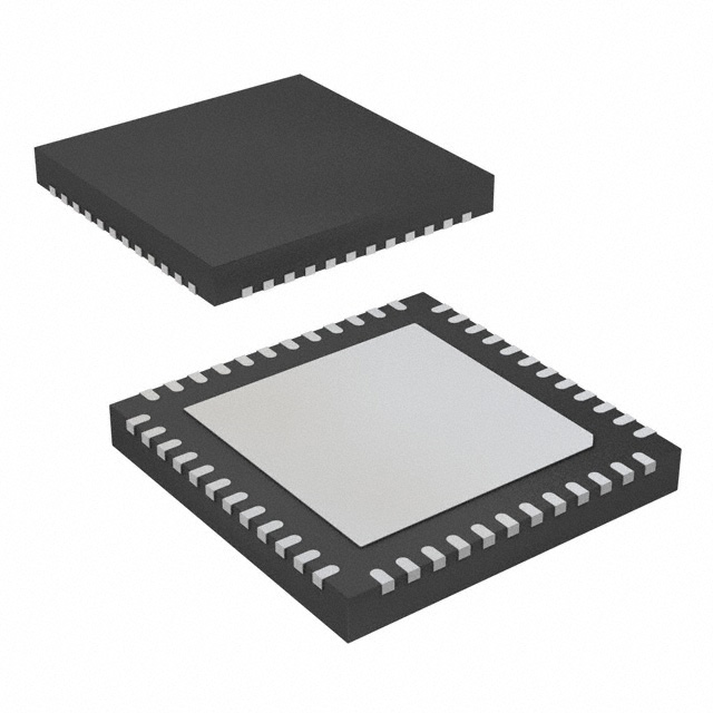


 工商网监
湘ICP备2023018690号
工商网监
湘ICP备2023018690号
