SAM3S8 / SAM3SD8
Atmel | SMART ARM-based Flash MCU
DATASHEET
Description
The Atmel ® | SMART SAM3S8/SD8 series is a member of a family of Flash
microcontrollers based on the high performance 32-bit ARM® Cortex®-M3 RISC
processor. It operates at a maximum speed of 64 MHz and features 512 Kbytes of
Flash (dual plane on SAM3SD8) and 64 Kbytes of SRAM. The peripheral set
includes a Full Speed USB Device port with embedded transceiver, a High Speed
MCI for SDIO/SD/MMC, an External Bus Interface featuring a Static Memory
Controller providing connection to SRAM, PSRAM, NOR Flash, LCD Module and
NAND Flash, 2(3) USARTs (3 on SAM3SD8C), 2 UARTs, 2 TWIs, 3 SPIs, an I2S,
as well as a PWM timer, two 3-channel general-purpose 16-bit timers (with
stepper motor and quadrature decoder logic support), an RTC, a 12-bit ADC, a
12-bit DAC and an analog comparator.
The SAM3S8/SD8 series is ready for capacitive touch thanks to the QTouch ®
library, offering an easy way to implement buttons, wheels and sliders.
The SAM3S8/SD8 device is a medium range general purpose microcontroller with
the best ratio in terms of reduced power consumption, processing power and
peripheral set. This enables the SAM3S8/SD8 to sustain a wide range of
applications including consumer, industrial control, and PC peripherals.
It operates from 1.62V to 3.6V and is available in 64- and 100-pin QFP, 64-pin
QFN, and 100-pin BGA packages.
The SAM3S8/SD8 series is the ideal migration path from the SAM7S series for
applications that require more performance. The SAM3S8/SD8 series is pin-to-pin
compatible with the SAM7S series.
Atmel-11090B-ATARM-SAM3S8-SAM3SD8-Datasheet_18-Dec-14
�Features
2
Core
̶ ARM Cortex-M3 revision 2.0 running at up to 64 MHz
̶ Memory Protection Unit (MPU)
̶ Thumb®-2 instruction set
Pin-to-pin compatible with AT91SAM7S legacy products (64-pin versions), SAM3S4/2/1 products
Memories
̶ 512 Kbytes Single Plane (SAM3S8) embedded Flash, 128-bit wide access, memory accelerator
̶ 512 Kbytes Dual Plane (SAM3SD8) embedded Flash, 128-bit wide access, memory accelerator
̶ 64 Kbytes embedded SRAM
̶ 16 Kbytes ROM with embedded boot loader routines (UART, USB) and IAP routines
̶ 8-bit Static Memory Controller (SMC): SRAM, PSRAM, NOR and NAND Flash support
System
̶ Embedded voltage regulator for single supply operation
̶ Power-on-Reset (POR), Brown-out Detector (BOD) and Watchdog for safe operation
̶ Quartz or ceramic resonator oscillators: 3 to 20 MHz main power with Failure Detection and optional low-power
32.768 kHz for RTC or device clock
̶ RTC with Gregorian and Persian Calendar mode, waveform generation in low-power modes
̶ RTC clock calibration circuitry for 32.768 kHz crystal frequency compensation
̶ High precision 8/12 MHz factory trimmed internal RC oscillator with 4 MHz default frequency for device startup.
In-application trimming access for frequency adjustment
̶ Slow Clock Internal RC oscillator as permanent low-power mode device clock
̶ Two PLLs up to 130 MHz for device clock and for USB
̶ Temperature Sensor
̶ Up to 24 peripheral DMA (PDC) channels
Low Power Modes
̶ Sleep and Backup modes, down to < 2 µA in Backup mode
̶ Ultra low-power RTC
Peripherals
̶ USB 2.0 Device: 12 Mbps, 2668 byte FIFO, up to 8 bidirectional Endpoints. On-Chip Transceiver
̶ Up to 3 USARTs with ISO7816, IrDA®, RS-485, SPI, Manchester and Modem Mode
̶ Two 2-wire UARTs
̶ Up to 2 Two Wire Interface (I2C compatible), 1 SPI, 1 Serial Synchronous Controller (I2S), 1 High Speed
Multimedia Card Interface (SDIO/SD Card/MMC)
̶ Two 3-channel 16-bit Timer Counters with capture, waveform, compare and PWM mode, Quadrature Decoder
Logic and 2-bit Gray Up/Down Counter for Stepper Motor
̶ 4-channel 16-bit PWM with Complementary Output, Fault Input, 12-bit Dead Time Generator Counter for Motor
Control
̶ 32-bit Real-time Timer and RTC with calendar and alarm features
̶ Up to 15-channel, 1Msps ADC with differential input mode and programmable gain stage and auto calibration
̶ One 2-channel 12-bit 1Msps DAC
̶ One Analog Comparator with flexible input selection, Selectable input hysteresis
̶ 32-bit Cyclic Redundancy Check Calculation Unit (CRCCU)
̶ Register Write Protection
SAM3S8 / SAM3SD8 [DATASHEET]
Atmel-11090B-ATARM-SAM3S8-SAM3SD8-Datasheet_18-Dec-14
�
I/O
̶ Up to 79 I/O lines with external interrupt capability (edge or level sensitivity), debouncing, glitch filtering and ondie Series Resistor Termination
̶ Three 32-bit Parallel Input/Output Controllers, Peripheral DMA assisted Parallel Capture Mode
Packages
̶ 100-lead LQFP (14 x 14 mm, pitch 0.5 mm)
̶ 100-ball TFBGA (9 x 9 mm, pitch 0.8 mm)
̶ 64-lead LQFP (10 x 10 mm, pitch 0.5 mm)
̶ 64-lead QFN (9 x 9 mm, pitch 0.5 mm)
SAM3S8 / SAM3SD8 [DATASHEET]
Atmel-11090B-ATARM-SAM3S8-SAM3SD8-Datasheet_18-Dec-14
3
�1.
Configuration Summary
The SAM3S8/SD8 series devices differ in memory size, package and features. Table 1-1 summarizes the
configurations of the device family.
Table 1-1.
Configuration Summary
Feature
SAM3S8B
SAM3S8C
SAM3SD8B
SAM3SD8C
Flash
512 Kbytes
512 Kbytes
512 Kbytes
512 Kbytes
SRAM
64 Kbytes
64 Kbytes
64 Kbytes
64 Kbytes
Package
LQFP64
QFN64
LQFP100
TFBGA100
LQFP64
QFN64
LQFP100
TFBGA100
Number of PIOs
47
79
47
(2)
79
(2)
16 channels(2)
16 channels
11 channels
2 channels
2 channels
2 channels
2 channels
Timer Counter
Channels
6(3)
6
6(3)
6
PDC Channels
22
22
24
24
12-bit ADC
11 channels
12-bit DAC
USART/UART
(1)
2/2
2/2
(1)
(1)
2/2
3/2(1)
HSMCI
1 port/4 bits
1 port/4 bits
1 port/4 bits
1 port/4 bits
External Bus Interface
–
8-bit data,
4 chip selects,
24-bit address
–
8-bit data,
4 chip selects,
24-bit address
Notes:
4
(2)
1.
2.
3.
Full Modem support on USART1.
One channel is reserved for internal temperature sensor.
Three TC channels are reserved for internal use.
SAM3S8 / SAM3SD8 [DATASHEET]
Atmel-11090B-ATARM-SAM3S8-SAM3SD8-Datasheet_18-Dec-14
�Block Diagram
TST
VD
N
DI
VD
System Controller
DO
UT
SAM3S8/SD8 100-pin version Block Diagram
JT
AG
SE
L
Figure 2-1.
TD
TDI
TMO
TC S/S
K/ WD
SW IO
CL
K
Voltage
Regulator
PCK0–PCK2
PLLA
PLLB
PMC
RC Osc
12/8/4 MHz
XIN
XOUT
3–20 MHz
Osc
JTAG & Serial Wire
In-Circuit Emulator
24-bit
Cortex M-3 Processor SysTick Counter
fmax 64 MHz
WKUPx
SUPC
XIN32
XOUT32
Osc 32 kHz
ERASE
RC 32 kHz
VDDIO
8 GPBR
MPU
VDDCORE
RTT
VDDPLL
RTCOUT0
POR
I/D
Flash
Unique
Identifier
NVIC
512 Kbytes Flash
SRAM
ROM
SAM3S8 Single Bank 64 Kbytes 16 Kbytes
SAM3SD8 Dual Bank
S
3-layer AHB Bus Matrix fmax 64 MHz
RTC
RSTC
NRST
WDT
Peripheral
Bridge
SM
2668 USB 2.0
bytes
Full
FIFO Speed
PIOA / PIOB / PIOC
TWCK0
TWD0
TWCK1
TWD1
URXD0
UTXD0
URXD1
UTXD1
RXD0
TXD0
SCK0
RTS0
CTS0
RXD1
TXD1
SCK1
RTS1
CTS1
DSR1
DTR1
RI1
DCD1
RXD2
TXD2
SCK2
RTS2
CTS2
TCLK[0:2]
TWI0
PDC
TWI1
PDC
UART0
PDC
UART1
External Bus
Interface
NAND Flash
Logic
PDC
Static Memory
Controller
USART0
DDP
DDM
PIO
RTCOUT1
Transceiver
2.
PDC
PDC
PIODC[7:0]
PIODCEN1
PIODCEN2
PIODCCLK
USART1
PIO
PDC
USART2
(SAM3SD8 only)
NPCS0
NPCS1
NPCS2
NPCS3
MISO
MOSI
SPCK
TF
TK
TD
RD
RK
RF
PDC
PDC
SPI
Timer Counter 0
TIOA[0:2]
TIOB[0:2]
TC[0..2]
TCLK[3:5]
Timer Counter 1
PDC
SSC
TIOA[3:5]
TIOB[3:5]
PDC
ADVREF
DAC0
DAC1
DATRG
MCCK
MCCDA
MCDA[0..3]
TC[3..5]
High Speed MCI
PWMH[0:3]
PWML[0:3]
PWMFI0
ADTRG
AD[0..14]
D[7:0]
A[0:23]
A21/NANDALE
A22/NANDCLE
NCS0
NCS1
NCS2
NCS3
NRD
NWE
NANDOE
NANDWE
NWAIT
PWM
PDC
Temp. Sensor
12-bit ADC
Analog
Comparator
ADVREF
ADC Ch.
CRC Unit
PDC
12-bit DAC
PDC
SAM3S8 / SAM3SD8 [DATASHEET]
Atmel-11090B-ATARM-SAM3S8-SAM3SD8-Datasheet_18-Dec-14
5
�TST
DO
N
DI
VD
System Controller
VD
JT
AG
SE
L
UT
SAM3S8/SD8 64-pin version Block Diagram
TD
TDI
TMO
TC S/S
K/ WD
SW IO
CL
K
Figure 2-2.
Voltage
Regulator
PCK0–PCK2
PLLA
PMC
RC Osc
12/8/4 MHz
XIN
XOUT
3–20 MHz
Osc
JTAG & Serial Wire
In-Circuit Emulator
24-bit
Cortex M-3 Processor SysTick Counter
fmax 64 MHz
WKUPx
SUPC
XIN32
XOUT32
Osc 32 kHz
ERASE
RC 32 kHz
VDDIO
8 GPBR
MPU
VDDCORE
RTT
VDDPLL
RTCOUT0
POR
I/D
Flash
Unique
Identifier
NVIC
PLLB
512 Kbytes Flash
SRAM
ROM
SAM3S8 Single Bank 64 Kbytes 16 Kbytes
SAM3SD8 Dual Bank
S
3-layer AHB Bus Matrix fmax 64 MHz
RSTC
NRST
WDT
Peripheral
Bridge
SM
2668 USB 2.0
bytes
Full
FIFO Speed
PIOA / PIOB
TWCK0
TWD0
TWI0
TWCK1
TWD1
TWI1
URXD0
UTXD0
UART0
URXD1
UTXD1
UART1
RXD0
TXD0
SCK0
RTS0
CTS0
DDP
DDM
PDC
PDC
PDC
PDC
PIODC[7:0]
PIODCEN1
PIODCEN2
PIODCCLK
PIO
PDC
USART0
PDC
PDC
SPI
PIO
USART1
PIO
RXD1
TXD1
SCK1
RTS1
CTS1
DSR1
DTR1
RI1
DCD1
Transceiver
RTC
RTCOUT1
PDC
PDC
TCLK[0:2]
TIOA[0:2]
TIOB[0:2]
ADTRG
AD[0..14]
SSC
TC[0..2]
PDC
PWM
PDC
6
MCCK
MCCDA
MCDA[0..3]
High Speed MCI
Temp. Sensor
12-bit ADC
ADVREF
DAC0
DAC1
DATRG
TF
TK
TD
RD
RK
RF
Timer Counter 0
PWMH[0:3]
PWML[0:3]
PWMFI0
NPCS0
NPCS1
NPCS2
NPCS3
MISO
MOSI
SPCK
PDC
Analog
Comparator
PDC
CRC Unit
12-bit DAC
SAM3S8 / SAM3SD8 [DATASHEET]
Atmel-11090B-ATARM-SAM3S8-SAM3SD8-Datasheet_18-Dec-14
ADVREF
ADC Ch.
�3.
Signal Description
Table 3-1 gives details on signal names classified by peripheral.
Table 3-1.
Signal Name
Signal Description List
Function
Active
Level
Type
Voltage
reference
Comments
Power Supplies
VDDIO
Peripherals I/O Lines and USB
transceiver Power Supply
Power
1.62V to 3.6V
VDDIN
Voltage Regulator Input, ADC, DAC
and Analog Comparator Power Supply
Power
1.8V to 3.6V(4)
VDDOUT
Voltage Regulator Output
Power
1.8V Output
VDDPLL
Oscillator and PLL Power Supply
Power
1.62 V to 1.95V
VDDCORE
Power the core, the embedded
memories and the peripherals
Power
1.62V to 1.95V
GND
Ground
Ground
Supply Controller - SUPC
Reset State:
WKUPx
Wake Up input pins
Input
VDDIO
- PIO Input
- Internal Pull-up disabled
- Schmitt Trigger enabled(1)
Clocks, Oscillators and PLLs
XIN
Main Oscillator Input
XOUT
Main Oscillator Output
XIN32
Slow Clock Oscillator Input
XOUT32
Slow Clock Oscillator Output
Input
Reset State:
Output
- PIO Input
- Internal Pull-up disabled
Input
Output
VDDIO
- Schmitt Trigger enabled(1)
Reset State:
PCK0–PCK2
Programmable Clock Output
- PIO Input
Output
- Internal Pull-up enabled
- Schmitt Trigger enabled(1)
Real Time Clock - RTC
RTCOUT0
RTCOUT1
Programmable RTC waveform output
Programmable RTC waveform output
Output
Output
Reset State:
VDDIO
- PIO Input
- Internal Pull-up disabled
- Schmitt Trigger enabled(1)
SAM3S8 / SAM3SD8 [DATASHEET]
Atmel-11090B-ATARM-SAM3S8-SAM3SD8-Datasheet_18-Dec-14
7
�Table 3-1.
Signal Description List (Continued)
Signal Name
Function
Type
Active
Level
Voltage
reference
Comments
Serial Wire/JTAG Debug Port - SWJ-DP
TCK/SWCLK
Test Clock/Serial Wire Clock
Input
TDI
Test Data In
Input
TDO/TRACESWO
Test Data Out / Trace Asynchronous
Data Out
TMS/SWDIO
Test Mode Select /Serial Wire
Input/Output
JTAGSEL
JTAG Selection
Reset State:
- SWJ-DP Mode
Output
VDDIO
Input / I/O
Input
- Internal pull-up disabled(5)
- Schmitt Trigger enabled(1)
Permanent Internal pulldown
High
Flash Memory
Reset State:
Flash and NVM Configuration Bits
Erase Command
ERASE
- Erase Input
Input
High
VDDIO
- Internal pull-down
enabled
- Schmitt Trigger enabled(1)
Reset/Test
NRST
Synchronous Microcontroller Reset
TST
Test Select
I/O
Low
Permanent Internal pull-up
VDDIO
Input
Permanent Internal pulldown
Universal Asynchronous Receiver Transceiver - UARTx
URXDx
UART Receive Data
Input
UTXDx
UART Transmit Data
Output
PIO Controller - PIOA - PIOB - PIOC
PA0–PA31
Parallel IO Controller A
I/O
PB0–PB14
Parallel IO Controller B
I/O
PC0–PC31
Parallel IO Controller C
I/O
Reset State:
VDDIO
Parallel Capture Mode Data
Input
PIODCCLK
Parallel Capture Mode Clock
Input
PIODCEN1–2
Parallel Capture Mode Enable
Input
VDDIO
External Bus Interface
D0–D7
Data Bus
A0–A23
Address Bus
NWAIT
External Wait Signal
I/O
Output
Input
Low
Static Memory Controller - SMC
NCS0–NCS3
Chip Select Lines
Output
Low
NRD
Read Signal
Output
Low
NWE
Write Enable
Output
Low
8
SAM3S8 / SAM3SD8 [DATASHEET]
Atmel-11090B-ATARM-SAM3S8-SAM3SD8-Datasheet_18-Dec-14
- Internal pull-up enabled
- Schmitt Trigger enabled(1)
PIO Controller - Parallel Capture Mode
PIODC0–PIODC7
- PIO or System IOs(2)
�Table 3-1.
Signal Description List (Continued)
Signal Name
Function
Type
Active
Level
Voltage
reference
Comments
NAND Flash Logic
NANDOE
NAND Flash Output Enable
Output
Low
NANDWE
NAND Flash Write Enable
Output
Low
High Speed Multimedia Card Interface - HSMCI
MCCK
Multimedia Card Clock
I/O
MCCDA
Multimedia Card Slot A Command
I/O
MCDA0–MCDA3
Multimedia Card Slot A Data
I/O
Universal Synchronous Asynchronous Receiver Transmitter - USARTx
SCKx
USARTx Serial Clock
I/O
TXDx
USARTx Transmit Data
I/O
RXDx
USARTx Receive Data
Input
RTSx
USARTx Request To Send
CTSx
USARTx Clear To Send
DTR1
USART1 Data Terminal Ready
DSR1
USART1 Data Set Ready
DCD1
USART1 Data Carrier Detect
RI1
USART1 Ring Indicator
Output
Input
I/O
Input
Output
Input
Synchronous Serial Controller - SSC
TD
SSC Transmit Data
Output
RD
SSC Receive Data
Input
TK
SSC Transmit Clock
I/O
RK
SSC Receive Clock
I/O
TF
SSC Transmit Frame Sync
I/O
RF
SSC Receive Frame Sync
I/O
Timer/Counter - TC
TCLKx
TC Channel x External Clock Input
Input
TIOAx
TC Channel x I/O Line A
I/O
TIOBx
TC Channel x I/O Line B
I/O
Pulse Width Modulation Controller - PWMC
PWMHx
PWM Waveform Output High for
channel x
PWMLx
PWM Waveform Output Low for
channel x
PWMFI0
PWM Fault Input
Output
Output
Only output in
complementary mode
when dead time insertion is
enabled.
Input
SAM3S8 / SAM3SD8 [DATASHEET]
Atmel-11090B-ATARM-SAM3S8-SAM3SD8-Datasheet_18-Dec-14
9
�Table 3-1.
Signal Description List (Continued)
Signal Name
Function
Type
Active
Level
Voltage
reference
Comments
Serial Peripheral Interface - SPI
MISO
Master In Slave Out
I/O
MOSI
Master Out Slave In
I/O
SPCK
SPI Serial Clock
I/O
SPI_NPCS0
SPI Peripheral Chip Select 0
I/O
Low
SPI_NPCS1–
SPI_NPCS3
SPI Peripheral Chip Select
Output
Low
Two-Wire Interface - TWI
TWDx
TWIx Two-wire Serial Data
I/O
TWCKx
TWIx Two-wire Serial Clock
I/O
Analog
ADC, DAC and Analog Comparator
Reference
ADVREF
Analog
12-bit Analog-to-Digital Converter - ADC
AD0–AD14
Analog Inputs
Analog, Digital
ADTRG
ADC Trigger
Input
VDDIO
12-bit Digital-to-Analog Converter - DAC
DAC0–DAC1
Analog output
DACTRG
DAC Trigger
Analog, Digital
Input
VDDIO
Fast Flash Programming Interface - FFPI
PGMEN0–
PGMEN2
Programming Enabling
Input
PGMM0–PGMM3
Programming Mode
Input
PGMD0–PGMD15
Programming Data
I/O
PGMRDY
Programming Ready
Output
High
PGMNVALID
Data Direction
Output
Low
PGMNOE
Programming Read
Input
Low
PGMCK
Programming Clock
Input
PGMNCMD
Programming Command
Input
VDDIO
VDDIO
Low
USB Full Speed Device
DDM
USB Full Speed Data -
DDP
USB Full Speed Data +
Note:
10
1.
2.
3.
4.
5.
Reset State:
Analog, Digital
VDDIO
- USB Mode
- Internal Pull-down(3)
Schmitt Triggers can be disabled through PIO registers.
Some PIO lines are shared with System I/Os.
Refer to USB Section of the product Electrical Characteristics for information on Pull-down value in USB Mode.
See “Typical Powering Schematics” Section for restrictions on voltage range of Analog Cells.
TDO pin is set in input mode when the Cortex-M3 Core is not in debug mode. Thus the internal pull-up corresponding to this
PIO line must be enabled to avoid current consumption due to floating input.
SAM3S8 / SAM3SD8 [DATASHEET]
Atmel-11090B-ATARM-SAM3S8-SAM3SD8-Datasheet_18-Dec-14
�4.
Package and Pinout
SAM3S8/SD8 devices are pin-to-pin compatible with AT91SAM7S legacy products for 64-pin version.
Furthermore, SAM3S8/SD8 products have new functionalities referenced in italic in Table 4-1, Table 4-3.
4.1
SAM3S8C/8DC Package and Pinout
4.1.1
100-Lead LQFP Package Outline
Figure 4-1.
Orientation of the 100-lead LQFP Package
75
51
76
50
100
26
1
4.1.2
25
100-ball TFBGA Package Outline
The 100-ball TFBGA package has a 0.8 mm ball pitch and respects Green Standards. The package dimensions
are 9 x 9 x 1.1 mm. Figure 4-2 shows the orientation of the 100-ball TFBGA package.
Figure 4-2.
Orientation of the 100-ball TFBGA Package
TOP VIEW
10
9
8
7
6
5
4
3
2
1
BALL A1
A
B
C
D
E
F
G
H
J
K
SAM3S8 / SAM3SD8 [DATASHEET]
Atmel-11090B-ATARM-SAM3S8-SAM3SD8-Datasheet_18-Dec-14
11
�4.1.3
100-Lead LQFP Pinout
Table 4-1.
SAM3S8C/SD8C 100-lead LQFP pinout
1
ADVREF
26
GND
51
TDI/PB4
76
TDO/TRACESWO/PB5
2
GND
27
VDDIO
52
PA6/PGMNOE
77
JTAGSEL
3
PB0/AD4
28
PA16/PGMD4
53
PA5/PGMRDY
78
PC18
4
PC29/AD13
29
PC7
54
PC28
79
TMS/SWDIO/PB6
5
PB1/AD5
30
PA15/PGMD3
55
PA4/PGMNCMD
80
PC19
6
PC30/AD14
31
PA14/PGMD2
56
VDDCORE
81
PA31
7
PB2/AD6
32
PC6
57
PA27/PGMD15
82
PC20
8
PC31
33
PA13/PGMD1
58
PC8
83
TCK/SWCLK/PB7
9
PB3/AD7
34
PA24/PGMD12
59
PA28
84
PC21
10
VDDIN
35
PC5
60
NRST
85
VDDCORE
11
VDDOUT
36
VDDCORE
61
TST
86
PC22
12
PA17/PGMD5/AD0
37
PC4
62
PC9
87
ERASE/PB12
13
PC26
38
PA25/PGMD13
63
PA29
88
DDM/PB10
14
PA18/PGMD6/AD1
39
PA26/PGMD14
64
PA30
89
DDP/PB11
15
PA21/PGMD9/AD8
40
PC3
65
PC10
90
PC23
16
VDDCORE
41
PA12/PGMD0
66
PA3
91
VDDIO
17
PC27
42
PA11/PGMM3
67
PA2/PGMEN2
92
PC24
18
PA19/PGMD7/AD2
43
PC2
68
PC11
93
PB13/DAC0
19
PC15/AD11
44
PA10/PGMM2
69
VDDIO
94
PC25
20
PA22/PGMD10/AD9
45
GND
70
GND
95
GND
21
PC13/AD10
46
PA9/PGMM1
71
PC14
96
PB8/XOUT
22
PA23/PGMD11
47
PC1
72
PA1/PGMEN1
97
PB9/PGMCK/XIN
23
PC12/AD12
48
PA8/XOUT32/PGMM0
73
PC16
98
VDDIO
24
PA20/PGMD8/AD3
49
PA7/XIN32/PGMNVALID
74
PA0/PGMEN0
99
PB14/DAC1
25
PC0
50
VDDIO
75
PC17
100
VDDPLL
12
SAM3S8 / SAM3SD8 [DATASHEET]
Atmel-11090B-ATARM-SAM3S8-SAM3SD8-Datasheet_18-Dec-14
�4.1.4
100-Ball TFBGA Pinout
Table 4-2.
SAM3S8C/SD8C 100-ball TFBGA pinout
A1
PB1/AD5
C6
TCK/SWCLK/PB7
F1
PA18/PGMD6/AD1
H6
PC4
A2
PC29
C7
PC16
F2
PC26
H7
PA11/PGMM3
A3
VDDIO
C8
PA1/PGMEN1
F3
VDDOUT
H8
PC1
A4
PB9/PGMCK/XIN
C9
PC17
F4
GND
H9
PA6/PGMNOE
A5
PB8/XOUT
C10
PA0/PGMEN0
F5
VDDIO
H10
TDI/PB4
A6
PB13/DAC0
D1
PB3/AD7
F6
PA27/PGMD15
J1
PC15/AD11
A7
DDP/PB11
D2
PB0/AD4
F7
PC8
J2
PC0
A8
DDM/PB10
D3
PC24
F8
PA28
J3
PA16/PGMD4
A9
TMS/SWDIO/PB6
D4
PC22
F9
TST
J4
PC6
A10
JTAGSEL
D5
GND
F10
PC9
J5
PA24/PGMD12
B1
PC30
D6
GND
G1
PA21/PGMD9/AD8
J6
PA25/PGMD13
B2
ADVREF
D7
VDDCORE
G2
PC27
J7
PA10/PGMM2
B3
GNDANA
D8
PA2/PGMEN2
G3
PA15/PGMD3
J8
GND
B4
PB14/DAC1
D9
PC11
G4
VDDCORE
J9
VDDCORE
B5
PC21
D10
PC14
G5
VDDCORE
J10
VDDIO
B6
PC20
E1
PA17/PGMD5/AD0
G6
PA26/PGMD14
K1
PA22/PGMD10/AD9
B7
PA31
E2
PC31
G7
PA12/PGMD0
K2
PC13/AD10
B8
PC19
E3
VDDIN
G8
PC28
K3
PC12/AD12
B9
PC18
E4
GND
G9
PA4/PGMNCMD
K4
PA20/PGMD8/AD3
B10 TDO/TRACESWO/PB5
E5
GND
G10
PA5/PGMRDY
K5
PC5
C1
PB2/AD6
E6
NRST
H1
PA19/PGMD7/AD2
K6
PC3
C2
VDDPLL
E7
PA29/AD13
H2
PA23/PGMD11
K7
PC2
C3
PC25
E8
PA30/AD14
H3
PC7
K8
PA9/PGMM1
C4
PC23
E9
PC10
H4
PA14/PGMD2
K9
PA8/XOUT32/PGMM0
C5
ERASE/PB12
E10
PA3
H5
PA13/PGMD1
K10 PA7/XIN32/PGMNVALID
SAM3S8 / SAM3SD8 [DATASHEET]
Atmel-11090B-ATARM-SAM3S8-SAM3SD8-Datasheet_18-Dec-14
13
�4.2
SAM3S8B/D8B Package and Pinout
4.2.1
64-Lead LQFP Package Outline
Figure 4-3.
Orientation of the 64-lead LQFP Package
33
48
49
32
64
17
16
1
4.2.2
64-lead QFN Package Outline
Figure 4-4.
Orientation of the 64-lead QFN Package
64
1
48
16
33
17
14
49
SAM3S8 / SAM3SD8 [DATASHEET]
Atmel-11090B-ATARM-SAM3S8-SAM3SD8-Datasheet_18-Dec-14
TOP VIEW
32
�4.2.3
64-Lead LQFP and QFN Pinout
Table 4-3.
64-pin SAM3S8B/D8B pinout
1
ADVREF
17
GND
33
TDI/PB4
49
TDO/TRACESWO/PB5
2
GND
18
VDDIO
34
PA6/PGMNOE
50
JTAGSEL
3
PB0/AD4
19
PA16/PGMD4
35
PA5/PGMRDY
51
TMS/SWDIO/PB6
4
PB1/AD5
20
PA15/PGMD3
36
PA4/PGMNCMD
52
PA31
5
PB2/AD6
21
PA14/PGMD2
37
PA27/PGMD15
53
TCK/SWCLK/PB7
6
PB3/AD7
22
PA13/PGMD1
38
PA28
54
VDDCORE
7
VDDIN
23
PA24/PGMD12
39
NRST
55
ERASE/PB12
8
VDDOUT
24
VDDCORE
40
TST
56
DDM/PB10
9
PA17/PGMD5/AD0
25
PA25/PGMD13
41
PA29
57
DDP/PB11
10
PA18/PGMD6/AD1
26
PA26/PGMD14
42
PA30
58
VDDIO
11
PA21/PGMD9/AD8
27
PA12/PGMD0
43
PA3
59
PB13/DAC0
12
VDDCORE
28
PA11/PGMM3
44
PA2/PGMEN2
60
GND
13
PA19/PGMD7/AD2
29
PA10/PGMM2
45
VDDIO
61
XOUT/PB8
14
PA22/PGMD10/AD9
30
PA9/PGMM1
46
GND
62
XIN/PGMCK/PB9
15
PA23/PGMD11
31
PA8/XOUT32/PGMM0
47
PA1/PGMEN1
63
PB14/DAC1
16
PA20/PGMD8/AD3
32
PA7/XIN32/PGMNVALID
48
PA0/PGMEN0
64
VDDPLL
Note: The bottom pad of the QFN package must be connected to ground.
SAM3S8 / SAM3SD8 [DATASHEET]
Atmel-11090B-ATARM-SAM3S8-SAM3SD8-Datasheet_18-Dec-14
15
�5.
Power Considerations
5.1
Power Supplies
The SAM3S8/SD8 has several types of power supply pins:
VDDCORE pins: Power the core, the embedded memories and the peripherals. Voltage ranges from 1.62V
to 1.95V.
VDDIO pins: Power the Peripherals I/O lines (Input/Output Buffers), USB transceiver, Backup part, 32 kHz
crystal oscillator and oscillator pads. Voltage ranges from 1.62V to 3.6V.
VDDIN pin: Voltage Regulator Input, ADC, DAC and Analog Comparator Power Supply. Voltage ranges from
1.8V to 3.6V.
VDDPLL pin: Powers the PLLA, PLLB, the Fast RC and the 3 to 20 MHz oscillator. Voltage ranges from
1.62V to 1.95V.
5.2
Power-up Considerations
5.2.1
VDDIO Versus VDDCORE
VDDIO must always be higher than or equal to VDDCORE.
VDDIO must reach its minimum operating voltage (1.62 V) before VDDCORE has reached the following
thresholds:
the minimum VT+ of the core power supply brownout detector (1.36 V)
the minimum value of tRST (100 µs)
If VDDCORE rises at the same time as VDDIO, the VDDIO rising slope must be higher than or equal to 5 V/ms.
If VDDCORE is powered by the internal regulator, all power-up considerations are met.
Figure 5-1.
VDDCORE and VDDIO Constraints at Startup
Supply (V)
VDDIO
VDDIO(min)
VDDCORE
VDDCORE(min)
VT+
tRST
Core supply POR output
SLCK
16
SAM3S8 / SAM3SD8 [DATASHEET]
Atmel-11090B-ATARM-SAM3S8-SAM3SD8-Datasheet_18-Dec-14
Time (t)
�5.2.2
VDDIO Versus VDDIN
At power-up, VDDIO needs to reach 0.6 V before VDDIN reaches 1.0 V.
VDDIO voltage needs to be equal to or below (VDDIN voltage + 0.5 V).
5.3
Voltage Regulator
The SAM3S8/SD8 embeds a voltage regulator that is managed by the Supply Controller.
This internal regulator is designed to supply the internal core of SAM3S8/SD8. It features two operating modes:
In Normal mode, the voltage regulator consumes less than 700 µA static current and draws 80 mA of output
current. Internal adaptive biasing adjusts the regulator quiescent current depending on the required load
current. In Wait Mode quiescent current is only 7 µA.
In Backup mode, the voltage regulator consumes less than 1 µA while its output (VDDOUT) is driven
internally to GND. The default output voltage is 1.80 V and the start-up time to reach Normal mode is less
than 100 µs.
For adequate input and output power supply decoupling/bypassing, refer to Table 41-3 ”1.8V Voltage Regulator
Characteristics” in Section 41. “SAM3S8/SD8 Electrical Characteristics”.
5.4
Typical Powering Schematics
The SAM3S8/SD8 supports a 1.62–3.6 V single supply mode. The internal regulator input is connected to the
source and its output feeds VDDCORE. Figure 5-2 shows the power schematics.
As VDDIN powers the voltage regulator, the ADC, DAC and the analog comparator, when the user does not want
to use the embedded voltage regulator, it can be disabled by software via the SUPC (note that this is different from
Backup mode).
Figure 5-2.
Single Supply
VDDIO
USB
Transceivers
Main Supply
(1.8–3.6 V)
ADC, DAC,
Analog Comp.
VDDIN
VDDOUT
Voltage
Regulator
VDDCORE
VDDPLL
Note:
Restrictions
For USB, VDDIO needs to be greater than 3.0 V.
For ADC, VDDIN needs to be greater than 2.0 V.
For DAC, VDDIN needs to be greater than 2.4 V.
For Analog Comparator, VDDIN needs to be greater than 2.0 V.
SAM3S8 / SAM3SD8 [DATASHEET]
Atmel-11090B-ATARM-SAM3S8-SAM3SD8-Datasheet_18-Dec-14
17
�Figure 5-3.
Core Externally Supplied
VDDIO
Main Supply
(1.62–3.6 V)
USB
Transceivers
Can be the
same supply
ADC, DAC, Analog
Comparator Supply
(2.0–3.6 V)
ADC, DAC,
Analog Comp.
VDDIN
VDDOUT
VDDCORE Supply
(1.62–1.95 V)
Voltage
Regulator
VDDCORE
VDDPLL
Note:
Restrictions
For USB, VDDIO needs to be greater than 3.0 V.
For ADC, VDDIN needs to be greater than 2.0 V.
For DAC, VDDIN needs to be greater than 2.4 V.
For Analog Comparator, VDDIN needs to be greater than 2.0 V.
Figure 5-4 provides an example of the powering scheme when using a backup battery. Since the PIO state is
preserved when in Backup mode, any free PIO line can be used to switch off the external regulator by driving the
PIO line at low level (PIO is input, pull-up enabled after backup reset). External wake-up of the system can be from
a push button or any signal. See Section 5.7 “Wake-up Sources” for further details.
Figure 5-4.
Backup Battery
VDDIO
Backup
Battery
USB
Transceivers
+
ADC, DAC,
Analog Comp.
VDDIN
Main Supply
IN
OUT
3.3V
LDO
VDDOUT
Voltage
Regulator
VDDCORE
ON/OFF
VDDPLL
PIOx (Output)
WKUPx
External wakeup signal
Note: The two diodes provide a “switchover circuit” (for illustration purpose) between the backup battery and the
main supply when the system is put inbackup mode.
Note:
18
Restrictions
For ADC, VDDIN needs to be greater than 2.0 V.
For DAC, VDDIN needs to be greater than 2.4 V.
For Analog Comparator, VDDIN needs to be greater than 2.0 V.
SAM3S8 / SAM3SD8 [DATASHEET]
Atmel-11090B-ATARM-SAM3S8-SAM3SD8-Datasheet_18-Dec-14
�5.5
Active Mode
Active mode is the normal running mode with the core clock running from the fast RC oscillator, the main crystal
oscillator or the PLLA. The power management controller can be used to adapt the frequency and to disable the
peripheral clocks.
5.6
Low-power Modes
The various low-power modes of the SAM3S8/SD8 are described below.
5.6.1
Backup Mode
The purpose of Backup mode is to achieve the lowest power consumption possible in a system which is
performing periodic wake-ups to perform tasks but not requiring fast startup time (< 0.1 ms). Total current
consumption is 1.5 µA typical.
The Supply Controller, zero-power power-on reset, RTT, RTC, Backup registers and 32 kHz oscillator (RC or
crystal oscillator selected by software in the Supply Controller) are running. The regulator and the core supply are
off.
Backup mode is based on the Cortex-M3 deep sleep mode with the voltage regulator disabled.
The SAM3S8/SD8 can be awakened from this mode through pins WKUP0–15, the supply monitor (SM), the RTT
or RTC wake-up event.
Backup mode is entered by using WFE instructions with the SLEEPDEEP bit in the Cortex-M3 System Control
Register set to 1. (See the power management description in Section 10. “ARM Cortex-M3 Processor”.)
Exit from Backup mode happens if one of the following enable wake up events occurs:
5.6.2
Level transition, configurable debouncing on pins WKUPEN0–15
Supply Monitor alarm
RTC alarm
RTT alarm
Wait Mode
The purpose of the wait mode is to achieve very low power consumption while maintaining the whole device in a
powered state for a startup time of less than 10 µs. Current Consumption in Wait mode is typically 20 µA (total
current consumption) if the internal voltage regulator is used or 12 µA if an external regulator is used.
In this mode, the clocks of the core, peripherals and memories are stopped. However, the core, peripherals and
memories power supplies are still powered. From this mode, a fast start up is available.
This mode is entered via Wait for Event (WFE) instructions with LPM = 1 (Low Power Mode bit in PMC Fast
Startup Mode Register (PMC_FSMR)). The Cortex-M3 is able to handle external events or internal events in order
to wake-up the core (WFE). This is done by configuring the external lines WKUP0–15 as fast startup wake-up pins
(refer to Section 5.8 “Fast Startup”). RTC or RTT Alarm and USB wake-up events can be used to wake up the CPU
(exit from WFE).
Entering Wait Mode:
Select the 4/8/12 MHz fast RC oscillator as Main Clock
Set the LPM bit in the PMC_FSMR
Execute the Wait-For-Event (WFE) instruction of the processor
Note:
Internal Main clock resynchronization cycles are necessary between the writing of MOSCRCEN bit and the effective
entry in Wait mode. Depending on the user application, waiting for MOSCRCEN bit to be cleared is recommended to
ensure that the core will not execute undesired instructions.
SAM3S8 / SAM3SD8 [DATASHEET]
Atmel-11090B-ATARM-SAM3S8-SAM3SD8-Datasheet_18-Dec-14
19
�5.6.3
Sleep Mode
The purpose of sleep mode is to optimize power consumption of the device versus response time. In this mode,
only the core clock is stopped. The peripheral clocks can be enabled. The current consumption in this mode is
application dependent.
This mode is entered via Wait for Interrupt (WFI) or Wait for Event (WFE) instructions with LPM = 0 in
PMC_FSMR.
The processor can be awakened from an interrupt if WFI instruction of the Cortex M3 is used, or from an event if
the WFE instruction is used to enter this mode.
5.6.4
Low Power Mode Summary Table
The modes detailed above are the main low-power modes. Each part can be set to on or off separately and wake
up sources can be individually configured. Table 5-1 shows a summary of the configurations of the low-power
modes.
20
SAM3S8 / SAM3SD8 [DATASHEET]
Atmel-11090B-ATARM-SAM3S8-SAM3SD8-Datasheet_18-Dec-14
�Atmel-11090B-ATARM-SAM3S8-SAM3SD8-Datasheet_18-Dec-14
SAM3S8 / SAM3SD8 [DATASHEET]
21
ON
Wait
Sleep
ON
ON
OFF
Regulator
Mode Entry
WFE +
SLEEPDEEP bit = 1
WFE +
SLEEPDEEP bit = 0
+ LPM bit = 1
WFE or WFI +
SLEEPDEEP bit = 0
+ LPM bit = 0
Peripherals
OFF
(Not
powered)
Powered
(Not
clocked)
Powered(7)
(Not
clocked)
Entry mode = WFE Any
Enabled Interrupt and/or
Any Event from: Fast
start-up through
WKUP0–15 pins
RTC alarm
RTT alarm
USB wake-up
Clocked
back
Clocked
back
Any Event from: Fast
startup through
WKUP0–15 pins
RTC alarm
RTT alarm
USB wake-up
Entry mode = WFI
Interrupt Only
Reset
Core at
Wake Up
WKUP0–15 pins
SM alarm
RTC alarm
RTT alarm
Potential Wake-up
Sources
Previous state
saved
Previous state
saved
Previous state
saved
PIO State
while in Low
Power Mode
Unchanged
Unchanged
PIOA &
PIOB &
PIOC
Inputs with
pull ups
PIO State
at Wake Up
(6)
12 µA/20 µA(5)
< 2 µA typ(4)
(2) (3)
Consumption
(6)
< 10 µs
< 0.1 ms
Wake-up
Time(1)
1. When considering wake-up time, the time required to start the PLL is not taken into account. Once started, the device works with the 4/8/12 MHz fast RC
oscillator. The user has to add the PLL start-up time if it is needed in the system. The wake-up time is defined as the time taken for wake up until the first
instruction is fetched.
2. The external loads on PIOs are not taken into account in the calculation.
3. Supply Monitor current consumption is not included.
4. Total Current consumption.
5. Total current consumption (without using internal voltage regulator) / Total current consumption (using internal voltage regulator).
6. Depends on MCK frequency.
7. In this mode the core is supplied and not clocked but some peripherals can be clocked.
ON
Backup
Notes:
ON
Mode
Memory
Core
Low-power Mode Configuration Summary
SUPC, 32 kHz
Osc., RTC, RTT,
GPBRs, POR
(Backup Region)
Table 5-1.
�5.7
Wake-up Sources
The wake-up events allow the device to exit the Backup mode. When a wake-up event is detected, the Supply
Controller performs a sequence which automatically reenables the core power supply and the SRAM power
supply, if they are not already enabled.
Figure 5-5.
Wake-up Sources
SMEN
sm_out
RTCEN
rtc_alarm
Core
Supply
Restart
RTTEN
rtt_alarm
WKUPT0
WKUP0
Note:
22
WKUPDBC
WKUPEN1
WKUPIS1
SLCK
WKUPS
Debouncer
Falling/Rising
Edge
Detector
WKUPT15
WKUP15
WKUPIS0
Falling/Rising
Edge
Detector
WKUPT1
WKUP1
WKUPEN0
WKUPEN15
WKUPIS15
Falling/Rising
Edge
Detector
Before instructing the system to enter Backup mode, if the field WKUPDBC > 0, ensure that none of the
WKUPx pins that are enabled for a wake-up (exit from Backup mode) hold an active polarity. This is
checked by reading the pin status in the PIO Controller. If WKUPENx = 1 and the pin WKUPx holds an
active polarity, the system must not be instructed to enter Backup mode.
SAM3S8 / SAM3SD8 [DATASHEET]
Atmel-11090B-ATARM-SAM3S8-SAM3SD8-Datasheet_18-Dec-14
�5.8
Fast Startup
The SAM3S8/SD8 allows the processor to restart in a few microseconds while the processor is in wait mode or in
sleep mode. A fast start up can occur upon detection of a low level on one of the 19 wake-up inputs (WKUP0 to 15
+ SM + RTC + RTT).
The fast restart circuitry, as shown in Figure 5-6, is fully asynchronous and provides a fast start-up signal to the
Power Management Controller. As soon as the fast start-up signal is asserted, the PMC automatically restarts the
embedded 4 MHz Fast RC oscillator, switches the master clock on this 4 MHz clock and reenables the processor
clock.
Figure 5-6.
Fast Start-Up Sources
USBEN
usb_wakeup
RTCEN
rtc_alarm
RTTEN
rtt_alarm
FSTT0
WKUP0
Falling/Rising
Edge
Detector
fast_restart
FSTT1
WKUP1
Falling/Rising
Edge
Detector
FSTT15
WKUP15
Falling/Rising
Edge
Detector
SAM3S8 / SAM3SD8 [DATASHEET]
Atmel-11090B-ATARM-SAM3S8-SAM3SD8-Datasheet_18-Dec-14
23
�6.
Input/Output Lines
The SAM3S8/SD8 has several kinds of input/output (I/O) lines such as general purpose I/Os (GPIO) and system
I/Os. GPIOs can have alternate functionality due to multiplexing capabilities of the PIO controllers. The same PIO
line can be used whether in I/O mode or by the multiplexed peripheral. System I/Os include pins such as test pins,
oscillators, erase or analog inputs.
6.1
General Purpose I/O Lines
GPIO Lines are managed by PIO Controllers. All I/Os have several input or output modes such as pull-up or pulldown, input Schmitt triggers, multi-drive (open-drain), glitch filters, debouncing or input change interrupt.
Programming of these modes is performed independently for each I/O line through the PIO controller user
interface. For more details, refer to Section 28. “Parallel Input/Output Controller (PIO)”.
The input/output buffers of the PIO lines are supplied through VDDIO power supply rail.
The SAM3S8/SD8 embeds high-speed pads able to handle up to 32 MHz for HSMCI (MCK/2), 45 MHz for SPI
clock lines and 35 MHz on other lines. See Section 41.11 “AC Characteristics” for more details. Typical pull-up and
pull-down value is 100 kΩ for all I/Os.
Each I/O line also embeds an ODT (On-Die Termination), (see Figure 6-1). It consists of an internal series resistor
termination scheme for impedance matching between the driver output (SAM3S8/SD8) and the PCB trace
impedance preventing signal reflection. The series resistor helps to reduce IOs switching current (di/dt) thereby
reducing in turn, EMI. It also decreases overshoot and undershoot (ringing) due to inductance of interconnect
between devices or between boards. In conclusion ODT helps diminish signal integrity issues.
Figure 6-1.
On-Die Termination
Z0 ~ ZO + RODT
ODT
36 ohms Typ.
RODT
Receiver
SAM3 Driver with
ZO ~ 10 ohms
6.2
PCB Trace
Z0 ~ 50 ohms
System I/O Lines
System I/O lines are pins used by oscillators, test mode, reset and JTAG to name but a few. The SAM3S8/SD8
system I/O lines shared with PIO lines are described in Table 6-1.
These pins are software configurable as general purpose I/O or system pins. At startup the default function of
these pins is always used.
24
SAM3S8 / SAM3SD8 [DATASHEET]
Atmel-11090B-ATARM-SAM3S8-SAM3SD8-Datasheet_18-Dec-14
�Table 6-1.
System I/O Configuration Pin List
SYSTEM_IO
Bit Number
Default Function
After Reset
Other Function
12
ERASE
PB12
Low Level at
startup(1)
10
DDM
PB10
–
11
DDP
PB11
–
In Matrix User Interface Registers
7
TCK/SWCLK
PB7
–
6
TMS/SWDIO
PB6
–
(Refer to the System I/O Configuration Register
in Section 22. “Bus Matrix (MATRIX)”.)
5
TDO/TRACESWO
PB5
–
4
TDI
PB4
–
–
PA7
XIN32
–
–
PA8
XOUT32
–
–
PB9
XIN
–
–
PB8
XOUT
–
Constraints for
Normal Start
Configuration
(2)
(3)
Notes:
1. If PB12 is used as PIO input in user applications, a low level must be ensured at startup to prevent Flash erase before the
user application sets PB12 into PIO mode.
2. Refer to “Slow Clock Generator” of Section 16. “SAM3 Supply Controller (SUPC)”.
3. Refer to the 3 to 20 MHz Crystal Oscillator information in Section 26. “Power Management Controller (PMC)”.
6.2.1
Serial Wire JTAG Debug Port (SWJ-DP) Pins
The SWJ-DP pins are TCK/SWCLK, TMS/SWDIO, TDO/SWO, TDI and commonly provided on a standard 20-pin
JTAG connector defined by ARM. For more details about voltage reference and reset state, refer to Table 3-1 on
page 7.
At startup, SWJ-DP pins are configured in SWJ-DP mode to allow connection with debugging probe. Please refer
to Section 11. “Debug and Test Features”.
SWJ-DP pins can be used as standard I/Os to provide users more general input/output pins when the debug port
is not needed in the end application. Mode selection between SWJ-DP mode (System IO mode) and general IO
mode is performed through the AHB Matrix Special Function Registers (MATRIX_SFR). Configuration of the pad
for pull-up, triggers, debouncing and glitch filters is possible regardless of the mode.
The JTAGSEL pin is used to select the JTAG boundary scan when asserted at a high level. It integrates a
permanent pull-down resistor of about 15 kΩ to GND, so that it can be left unconnected for normal operations.
By default, the JTAG Debug Port is active. If the debugger host wants to switch to the Serial Wire Debug Port, it
must provide a dedicated JTAG sequence on TMS/SWDIO and TCK/SWCLK which disables the JTAG-DP and
enables the SW-DP. When the Serial Wire Debug Port is active, TDO/TRACESWO can be used for trace.
The asynchronous TRACE output (TRACESWO) is multiplexed with TDO. So the asynchronous trace can only be
used with SW-DP, not JTAG-DP. For more information about SW-DP and JTAG-DP switching, please refer to
Section 11. “Debug and Test Features”.
SAM3S8 / SAM3SD8 [DATASHEET]
Atmel-11090B-ATARM-SAM3S8-SAM3SD8-Datasheet_18-Dec-14
25
�6.3
Test Pin
The TST pin is used for JTAG Boundary Scan Manufacturing Test or Fast Flash programming mode of the
SAM3S8/SD8 series. The TST pin integrates a permanent pull-down resistor of about 15 kΩ to GND, so that it can
be left unconnected for normal operations. To enter fast programming mode, see the Fast Flash Programming
Interface (FFPI) section. For more on the manufacturing and test mode, refer to Section 11. “Debug and Test
Features”.
6.4
NRST Pin
The NRST pin is bidirectional. It is handled by the on-chip reset controller and can be driven low to provide a reset
signal to the external components or asserted low externally to reset the microcontroller. It will reset the Core and
the peripherals except the Backup region (RTC, RTT and Supply Controller). There is no constraint on the length
of the reset pulse and the reset controller can guarantee a minimum pulse length. The NRST pin integrates a
permanent pull-up resistor to VDDIO of about 100 kΩ. By default, the NRST pin is configured as an input.
6.5
ERASE Pin
The ERASE pin is used to reinitialize the Flash content (and some of its NVM bits) to an erased state (all bits read
as logic level 1). It integrates a pull-down resistor of about 100 kΩ to GND, so that it can be left unconnected for
normal operations.
This pin is debounced by SCLK to improve the glitch tolerance. When the ERASE pin is tied high during less than
100 ms, it is not taken into account. The pin must be tied high during more than 220 ms to perform a Flash erase
operation.
The ERASE pin is a system I/O pin and can be used as a standard I/O. At startup, the ERASE pin is not configured
as a PIO pin. If the ERASE pin is used as a standard I/O, startup level of this pin must be low to prevent unwanted
erasing. Refer to Section 9.3 “Peripheral Signal Multiplexing on I/O Lines” on page 33. Also, if the ERASE pin is
used as a standard I/O output, asserting the pin to low does not erase the Flash.
26
SAM3S8 / SAM3SD8 [DATASHEET]
Atmel-11090B-ATARM-SAM3S8-SAM3SD8-Datasheet_18-Dec-14
�7.
Memories
Figure 7-1.
SAM3S8/SD8 Product Mapping
0x00000000
Code
0x00000000
Address memory space
Peripherals
0x40000000
HSMCI
Boot Memory
Internal Flash
0x00800000
Internal ROM
0x00C00000
1 Mbyte
bit band
region
SSC
0x20000000
0x20100000
SPI
21
0x4000C000
Reserved
Undefined
0x40010000
0x24000000
0x40000000
22
0x40008000
SRAM
0x22000000
Reserved
0x1FFFFFFF
18
0x40004000
Code
0x00400000
32 Mbytes
bit band alias
+0x40
+0x80
Peripherals
TC0
0x60000000
0x61000000
0x62000000
0x63000000
0x64000000
SMC Chip Select 0
0x40014000
SMC Chip Select 3
+0x80
Reserved
TC3
26
TC1
0xA0000000
SMC Chip Select 2
TC2
25
TC1
External SRAM
+0x40
SMC Chip Select 1
TC1
24
TC0
External RAM
0x60000000
TC0
23
TC0
TC4
27
TC1
TC5
28
0x40018000
0xE0000000
TWI0
System
Reserved
0x9FFFFFFF
19
0x4001C000
0xFFFFFFFF
TWI1
20
0x40020000
0x400E0000
System Controller
PWM
USART1
0x400E0400
USART2
5
0x400E0600
16
0x40030000
UART0
Reserved
8
0x400E0740
15
0x4002C000
PMC
ID
14
0x40028000
MATRIX
block
peripheral
USART0
10
0x400E0200
offset
31
0x40024000
SMC
1 Mbyte
bit band
region
0x40034000
CHIPID
UDP
0x400E0800
UART1
ADC
9
0x400E0A00
29
0x4003C000
EFC
DACC
6
0x400E0C00
33
0x40038000
30
0x40040000
Reserved
ACC
0x400E0E00
CRCCU
11
0x400E1000
Reserved
12
0x400E0000
PIOC
System Controller
13
0x400E1400
0x400E2600
RSTC
Reserved
1
+0x10
35
0x40048000
PIOB
0x400E1200
34
0x40044000
PIOA
0x40100000
SUPC
Reserved
+0x30
0x40200000
RTT
3
+0x50
0x40400000
WDT
Reserved
4
+0x60
32 Mbytes
bit band alias
0x60000000
RTC
2
+0x90
GPBR
0x400E1600
Reserved
0x4007FFFF
SAM3S8 / SAM3SD8 [DATASHEET]
Atmel-11090B-ATARM-SAM3S8-SAM3SD8-Datasheet_18-Dec-14
27
�7.1
Embedded Memories
7.1.1
Internal SRAM
The SAM3S8 device (512-Kbytes, single bank flash) embeds a total of 64-Kbytes high-speed SRAM.
The SAM3SD8 device (512-Kbytes, dual bank flash) embeds a total of 64-Kbytes high-speed SRAM.
The SRAM is accessible over System Cortex-M3 bus at address 0x2000 0000.
The SRAM is in the bit band region. The bit band alias region is from 0x2200 0000 and 0x23FF FFFF.
7.1.2
Internal ROM
The SAM3S8/SD8 embeds an Internal ROM, which contains the SAM Boot Assistant (SAM-BA®), In Application
Programming (IAP) routines and Fast Flash Programming Interface (FFPI).
At any time, the ROM is mapped at address 0x0080 0000.
7.1.3
Embedded Flash
7.1.3.1
Flash Overview
The Flash of the SAM3S8 (512-Kbytes single bank flash) is organized in one bank of 2048 pages of 256 bytes.
The Flash of the SAM3SD8 (512-Kbytes, dual bank flash) is organized in two banks of 1024 pages of 256 bytes
each.
The Flash contains a 128-byte write buffer, accessible through a 32-bit interface.
7.1.3.2
Flash Power Supply
The Flash is supplied by VDDCORE.
7.1.3.3
Enhanced Embedded Flash Controller
The Enhanced Embedded Flash Controller (EEFC) manages accesses performed by the masters of the system. It
enables reading the Flash and writing the write buffer. It also contains a User Interface, mapped on the APB.
The Enhanced Embedded Flash Controller ensures the interface of the Flash block with the 32-bit internal bus. Its
128-bit wide memory interface increases performance.
The user can choose between high performance or lower current consumption by selecting either 128-bit or 64-bit
access. It also manages the programming, erasing, locking and unlocking sequences of the Flash using a full set
of commands.
One of the commands returns the embedded Flash descriptor definition that informs the system about the Flash
organization, thus making the software generic.
7.1.3.4
Flash Speed
The user needs to set the number of wait states depending on the frequency used:
For more details, refer to the “AC Characteristics” sub-section of the product “Electrical Characteristics”.
7.1.3.5
Lock Regions
Several lock bits are used to protect write and erase operations on lock regions. A lock region is composed of
several consecutive pages, and each lock region has its associated lock bit.
Table 7-1.
28
Lock bit number
Product
Number of Lock Bits
Lock Region Size
SAM3S8/SD8
16
32 kbytes (128 pages)
SAM3S8 / SAM3SD8 [DATASHEET]
Atmel-11090B-ATARM-SAM3S8-SAM3SD8-Datasheet_18-Dec-14
�If a locked-region’s erase or program command occurs, the command is aborted and the EEFC triggers an
interrupt.
The lock bits are software programmable through the EEFC User Interface. The command “Set Lock Bit” enables
the protection. The command “Clear Lock Bit” unlocks the lock region.
Asserting the ERASE pin clears the lock bits, thus unlocking the entire Flash.
7.1.3.6
Security Bit Feature
The SAM3S8/SD8 features a security bit, based on a specific General Purpose NVM bit (GPNVM bit 0). When the
security is enabled, any access to the Flash, SRAM, Core Registers and Internal Peripherals either through the
ICE interface or through the Fast Flash Programming Interface, is forbidden. This ensures the confidentiality of the
code programmed in the Flash.
This security bit can only be enabled, through the command “Set General Purpose NVM Bit 0” of the EEFC User
Interface. Disabling the security bit can only be achieved by asserting the ERASE pin at 1, and after a full Flash
erase is performed. When the security bit is deactivated, all accesses to the Flash, SRAM, Core registers, Internal
Peripherals are permitted.
It is important to note that the assertion of the ERASE pin should always be longer than 200 ms.
As the ERASE pin integrates a permanent pull-down, it can be left unconnected during normal operation.
However, it is safer to connect it directly to GND for the final application.
7.1.3.7
Calibration Bits
NVM bits are used to calibrate the brownout detector and the voltage regulator. These bits are factory configured
and cannot be changed by the user. The ERASE pin has no effect on the calibration bits.
7.1.3.8
Unique Identifier
Each device integrates its own 128-bit unique identifier. These bits are factory configured and cannot be changed
by the user. The ERASE pin has no effect on the unique identifier.
7.1.3.9
Fast Flash Programming Interface
The Fast Flash Programming Interface allows programming the device through either a serial JTAG interface or
through a multiplexed fully-handshaked parallel port. It allows gang programming with market-standard industrial
programmers.
The FFPI supports read, page program, page erase, full erase, lock, unlock and protect commands.
7.1.3.10 SAM-BA Boot
The SAM-BA Boot is a default Boot Program which provides an easy way to program in-situ the on-chip Flash
memory.
The SAM-BA Boot Assistant supports serial communication via the UART and USB.
The SAM-BA Boot provides an interface with SAM-BA Graphic User Interface (GUI).
The SAM-BA Boot is in ROM and is mapped in Flash at address 0x0 when GPNVM bit 1 is set to 0.
7.1.3.11 GPNVM Bits
The SAM3S8 features two GPNVM bits, whereas SAM3SD8 features three GPNVM bits. These bits can be
cleared or set respectively through the commands “Clear GPNVM Bit” and “Set GPNVM Bit” of the EEFC User
Interface.
The Flash of the SAM3S8 is composed of 512 Kbytes in a single bank, while the SAM3SD8 Flash is composed of
dual banks, each containing 256 Kbytes. The dual-bank function enables programming one bank while the other
one is read (typically while the application code is running). Only one EEFC (Flash controller) controls the two
banks. Note that it is not possible to program simultaneously, or read simultaneously, the dual banks of the Flash.
The first bank of 256 Kbytes is called Bank 0 and the second bank of 256 Kbytes, Bank 1.
SAM3S8 / SAM3SD8 [DATASHEET]
Atmel-11090B-ATARM-SAM3S8-SAM3SD8-Datasheet_18-Dec-14
29
�The SAM3SD8 embeds an additional GPNVM bit: GPNVM2.
Table 7-2.
7.1.4
General-purpose Non volatile Memory Bits
GPNVMBit[#]
Function
0
Security bit
1
Boot mode selection
2
Bank selection (Bank 0 or Bank 1) Only on SAM3SD8
Boot Strategies
The system always boots at address 0x0. To ensure maximum boot possibilities, the memory layout can be
changed via GPNVM.
A general purpose NVM (GPNVM) bit is used to boot either on the ROM (default) or from the Flash.
The GPNVM bit can be cleared or set respectively through the commands “Clear General-purpose NVM Bit” and
“Set General-purpose NVM Bit” of the EEFC User Interface.
Setting GPNVM Bit 1 selects the boot from the Flash, clearing it selects the boot from the ROM. Asserting ERASE
clears the GPNVM Bit 1 and thus selects the boot from the ROM by default.
Setting the GPNVM Bit 2 selects bank 1, clearing it selects the boot from bank 0. Asserting ERASE clears the
GPNVM Bit 2 and thus selects the boot from bank 0 by default.
7.2
External Memories
The SAM3S8/SD8 features one External Bus Interface to provide an interface to a wide range of external
memories and to any parallel peripheral.
30
SAM3S8 / SAM3SD8 [DATASHEET]
Atmel-11090B-ATARM-SAM3S8-SAM3SD8-Datasheet_18-Dec-14
�8.
System Controller
The System Controller is a set of peripherals, which allow handling of key elements of the system, such as power,
resets, clocks, time, interrupts, watchdog, etc.
8.1
System Controller and Peripherals Mapping
Please refer to Section 7-1 “SAM3S8/SD8 Product Mapping” on page 27.
All the peripherals are in the bit band region and are mapped in the bit band alias region.
8.2
Power-on-Reset, Brownout and Supply Monitor
The SAM3S8/SD8 embeds three features to monitor, warn and/or reset the chip:
8.2.1
Power-on-Reset on VDDIO
Brownout Detector on VDDCORE
Supply Monitor on VDDIO
Power-on-Reset
The Power-on-Reset monitors VDDIO. It is always activated and monitors voltage at start up but also during power
down. If VDDIO goes below the threshold voltage, the entire chip is reset. For more information, refer to Section
41. “SAM3S8/SD8 Electrical Characteristics”.
8.2.2
Brownout Detector on VDDCORE
The Brownout Detector monitors VDDCORE. It is active by default. It can be deactivated by software through the
Supply Controller (SUPC_MR). It is especially recommended to disable it during low-power modes such as wait or
sleep modes.
If VDDCORE goes below the threshold voltage, the reset of the core is asserted. For more information, refer to
Section 16. “SAM3 Supply Controller (SUPC)” and Section 41. “SAM3S8/SD8 Electrical Characteristics”.
8.2.3
Supply Monitor on VDDIO
The Supply Monitor monitors VDDIO. It is not active by default. It can be activated by software and is fully
programmable with 16 steps for the threshold (between 1.9V to 3.4V). It is controlled by the SUPC. A sample
mode is possible. It allows to divide the supply monitor power consumption by a factor of up to 2048. For more
information, refer to Section 16. “SAM3 Supply Controller (SUPC)” and Section 41. “SAM3S8/SD8 Electrical
Characteristics”.
SAM3S8 / SAM3SD8 [DATASHEET]
Atmel-11090B-ATARM-SAM3S8-SAM3SD8-Datasheet_18-Dec-14
31
�9.
Peripherals
9.1
Peripheral Identifiers
Table 9-1 defines the Peripheral Identifiers of the SAM3S8/SD8. A peripheral identifier is required for the control of
the peripheral interrupt with the Nested Vectored Interrupt Controller and control of the peripheral clock with the
Power Management Controller.
Table 9-1.
32
Peripheral Identifiers
Instance ID
Instance Name
NVIC Interrupt
0
SUPC
X
Supply Controller
1
RSTC
X
Reset Controller
2
RTC
X
Real Time Clock
3
RTT
X
Real Time Timer
4
WDT
X
Watchdog Timer
5
PMC
X
Power Management Controller
6
EEFC
X
Enhanced Embedded Flash Controller
7
–
–
–
Reserved
8
UART0
X
X
UART 0
9
UART1
X
X
UART 1
10
SMC
X
X
Static Memory Controller
11
PIOA
X
X
Parallel I/O Controller A
12
PIOB
X
X
Parallel I/O Controller B
13
PIOC
X
X
Parallel I/O Controller C
14
USART0
X
X
USART 0
15
USART1
X
X
USART 1
16
USART2
X
X
USART 2 (SAM3SD8 100 pins only)
17
–
–
–
Reserved
18
HSMCI
X
X
Multimedia Card Interface
19
TWI0
X
X
Two Wire Interface 0
20
TWI1
X
X
Two Wire Interface 1
21
SPI
X
X
Serial Peripheral Interface
22
SSC
X
X
Synchronous Serial Controller
23
TC0
X
X
Timer/Counter 0
24
TC1
X
X
Timer/Counter 1
25
TC2
X
X
Timer/Counter 2
26
TC3
X
X
Timer/Counter 3
27
TC4
X
X
Timer/Counter 4
28
TC5
X
X
Timer/Counter 5
29
ADC
X
X
Analog To Digital Converter
30
DACC
X
X
Digital To Analog Converter
SAM3S8 / SAM3SD8 [DATASHEET]
Atmel-11090B-ATARM-SAM3S8-SAM3SD8-Datasheet_18-Dec-14
PMC Clock Control
Instance Description
�Table 9-1.
9.2
Peripheral Identifiers (Continued)
Instance ID
Instance Name
NVIC Interrupt
PMC Clock Control
Instance Description
31
PWM
X
X
Pulse Width Modulation
32
CRCCU
X
X
CRC Calculation Unit
33
ACC
X
X
Analog Comparator
34
UDP
X
X
USB Device Port
APB/AHB Bridge
The SAM3S8/SD8 embeds One Peripheral Bridge. The peripherals of the bridge are clocked by MCK.
9.3
Peripheral Signal Multiplexing on I/O Lines
The SAM3S8/SD8 features two PIO controllers on 64-pin versions (PIOA and PIOB) or three PIO controllers on
the 100-pin version (PIOA, PIOB and PIOC), that multiplex the I/O lines of the peripheral set.
The SAM3S8/SD8 64-pin and 100-pin PIO Controllers control up to 32 lines. Each line can be assigned to one of
three peripheral functions: A, B or C. The multiplexing tables in the following tables define how the I/O lines of the
peripherals A, B and C are multiplexed on the PIO Controllers.
Note that some peripheral functions which are output only, might be duplicated within the tables.
SAM3S8 / SAM3SD8 [DATASHEET]
Atmel-11090B-ATARM-SAM3S8-SAM3SD8-Datasheet_18-Dec-14
33
�9.3.1
PIO Controller A Multiplexing
Table 9-2.
Multiplexing on PIO Controller A (PIOA)
I/O Line
Peripheral
A
Peripheral
B
Peripheral
C
PA0
PWMH0
TIOA0
A17
WKUP0
PA1
PWMH1
TIOB0
A18
WKUP1
PA2
PWMH2
SCK0
DATRG
WKUP2
PA3
TWD0
NPCS3
PA4
TWCK0
TCLK0
WKUP3
PA5
RXD0
NPCS3
WKUP4
PA6
TXD0
PCK0
PA7
RTS0
PWMH3
PA8
CTS0
ADTRG
PA9
URXD0
NPCS1
PA10
UTXD0
NPCS2
PA11
NPCS0
PWMH0
PA12
MISO
PWMH1
PA13
MOSI
PWMH2
PA14
SPCK
PWMH3
PA15
TF
TIOA1
PWML3
PIODCEN1
WKUP14
PA16
TK
TIOB1
PWML2
PIODCEN2
WKUP15
PA17
TD
PCK1
PWMH3
AD0
PA18
RD
PCK2
A14
AD1
PA19
RK
PWML0
A15
AD2/WKUP9
PA20
RF
PWML1
A16
AD3/WKUP10
PA21
RXD1
PCK1
PA22
TXD1
NPCS3
NCS2
PA23
SCK1
PWMH0
A19
PIODCCLK
64/100-pin versions
PA24
RTS1
PWMH1
A20
PIODC0
64/100-pin versions
PA25
CTS1
PWMH2
A23
PIODC1
64/100-pin versions
PA26
DCD1
TIOA2
MCDA2
PIODC2
64/100-pin versions
PA27
DTR1
TIOB2
MCDA3
PIODC3
64/100-pin versions
PA28
DSR1
TCLK1
MCCDA
PIODC4
64/100-pin versions
PA29
RI1
TCLK2
MCCK
PIODC5
64/100-pin versions
PA30
PWML2
NPCS2
MCDA0
PIODC6
PA31
NPCS1
PCK2
MCDA1
PIODC7
34
Peripheral
D
Extra
Function
System
Function
Comments
XIN32
WKUP5
PWMFI0
XOUT32
WKUP6
WKUP7
WKUP8
SAM3S8 / SAM3SD8 [DATASHEET]
Atmel-11090B-ATARM-SAM3S8-SAM3SD8-Datasheet_18-Dec-14
AD8
64/100-pin versions
AD9
64/100-pin versions
WKUP11
64/100-pin versions
64/100-pin versions
�9.3.2
PIO Controller B Multiplexing
Table 9-3.
Multiplexing on PIO Controller B (PIOB)
I/O Line
Peripheral A
Peripheral B
Peripheral C
Extra Function
PB0
PWMH0
AD4/RTCOUT0
PB1
PWMH1
AD5/RTCOUT1
PB2
URXD1
NPCS2
AD6/WKUP12
PB3
UTXD1
PCK2
AD7
PB4
TWD1
PWMH2
PB5
TWCK1
PWML0
System Function
Comments
TDI
WKUP13
TDO/TRACESW
O
PB6
TMS/SWDIO
PB7
TCK/SWCLK
PB8
XOUT
PB9
XIN
PB10
DDM
PB11
DDP
PB12
PWML1
ERASE
PB13
PWML2
PCK0
DAC0
64/100-pin versions
PB14
NPCS1
PWMH3
DAC1
64/100-pin versions
SAM3S8 / SAM3SD8 [DATASHEET]
Atmel-11090B-ATARM-SAM3S8-SAM3SD8-Datasheet_18-Dec-14
35
�9.3.3
PIO Controller C Multiplexing
Table 9-4.
Multiplexing on PIO Controller C (PIOC)
I/O Line
Peripheral A
Peripheral B
PC0
D0
PWML0
100-pin version
PC1
D1
PWML1
100-pin version
PC2
D2
PWML2
100-pin version
PC3
D3
PWML3
100-pin version
PC4
D4
NPCS1
100-pin version
PC5
D5
100-pin version
PC6
D6
100-pin version
PC7
D7
100-pin version
PC8
NWE
System Function
Comments
100-pin version
100-pin version
100-pin version
NANDOE
RXD2
PC10
NANDWE
TXD2(1)
PC11
NRD
PC12
NCS3
PC13
NWAIT
PWML0
PC14
NCS0
SCK2(1)
PC15
NCS1
PWML1
A21/NANDALE
Extra Function
(1)
PC9
PC16
Peripheral C
100-pin version
RTS2
AD12
100-pin version
AD10
100-pin version
100-pin version
AD11
100-pin version
(1)
100-pin version
(1)
100-pin version
PC17
A22/NANDCLE
PC18
A0
PWMH0
100-pin version
PC19
A1
PWMH1
100-pin version
PC20
A2
PWMH2
100-pin version
PC21
A3
PWMH3
100-pin version
PC22
A4
PWML3
100-pin version
PC23
A5
TIOA3
100-pin version
PC24
A6
TIOB3
100-pin version
PC25
A7
TCLK3
100-pin version
PC26
A8
TIOA4
100-pin version
PC27
A9
TIOB4
100-pin version
PC28
A10
TCLK4
100-pin version
PC29
A11
TIOA5
AD13
100-pin version
PC30
A12
TIOB5
AD14
100-pin version
PC31
A13
TCLK5
Note:
36
CTS2
1. USART2 only on SAM3SD8 in 100-pin package.
SAM3S8 / SAM3SD8 [DATASHEET]
Atmel-11090B-ATARM-SAM3S8-SAM3SD8-Datasheet_18-Dec-14
100-pin version
�10.
ARM Cortex-M3 Processor
10.1
About this section
This section provides the information required for application and system-level software development. It does not
provide information on debug components, features, or operation.
This material is for microcontroller software and hardware engineers, including those who have no experience of
ARM products.
Note: The information in this section is reproduced from source material provided to Atmel by ARM Ltd. in terms of
Atmel’s license for the ARM Cortex-M3 processor core. This information is copyright ARM Ltd., 2008 - 2009.
10.2
About the Cortex-M3 processor and core peripherals
The Cortex-M3 processor is a high performance 32-bit processor designed for the microcontroller market. It
offers significant benefits to developers, including:
outstanding processing performance combined with fast interrupt handling
enhanced system debug with extensive breakpoint and trace capabilities
efficient processor core, system and memories
ultra-low power consumption with integrated sleep modes
platform security, with integrated memory protection unit (MPU).
Figure 10-1.
Typical Cortex-M3 implementation
Cortex-M3
Processor
NVIC
Debug
Access
Port
Processor
Core
Serial
Wire
Viewer
Memory
Protection Unit
Flash
Patch
Data
Watchpoints
Bus Matrix
Code
Interface
SRAM and
Peripheral Interface
The Cortex-M3 processor is built on a high-performance processor core, with a 3-stage pipeline Harvard
architecture, making it ideal for demanding embedded applications. The processor delivers exceptional power
efficiency through an efficient instruction set and extensively optimized design, providing high-end processing
hardware including single-cycle 32x32 multiplication and dedicated hardware division.
To facilitate the design of cost-sensitive devices, the Cortex-M3 processor implements tightly-coupled system
components that reduce processor area while significantly improving interrupt handling and system debug
SAM3S8 / SAM3SD8 [DATASHEET]
Atmel-11090B-ATARM-SAM3S8-SAM3SD8-Datasheet_18-Dec-14
37
�®
capabilities. The Cortex-M3 processor implements a version of the Thumb instruction set, ensuring high code
density and reduced program memory requirements. The Cortex-M3 instruction set provides the exceptional
performance expected of a modern 32-bit architecture, with the high code density of 8-bit and 16-bit
microcontrollers.
The Cortex-M3 processor closely integrates a configurable nested interrupt controller (NVIC), to deliver industryleading interrupt performance. The NVIC provides up to 16 interrupt priority levels. The tight integration of the
processor core and NVIC provides fast execution of interrupt service routines (ISRs), dramatically reducing the
interrupt latency. This is achieved through the hardware stacking of registers, and the ability to suspend loadmultiple and store-multiple operations. Interrupt handlers do not require any assembler stubs, removing any code
overhead from the ISRs. Tail-chaining optimization also significantly reduces the overhead when switching from
one ISR to another.
To optimize low-power designs, the NVIC integrates with the sleep modes, that include a deep sleep function that
enables the entire device to be rapidly powered down.
10.2.1
System level interface
®
The Cortex-M3 processor provides multiple interfaces using AMBA technology to provide high speed, low latency
memory accesses. It supports unaligned data accesses and implements atomic bit manipulation that enables
faster peripheral controls, system spinlocks and thread-safe Boolean data handling.
The Cortex-M3 processor has a memory protection unit (MPU) that provides fine grain memory control, enabling
applications to implement security privilege levels, separating code, data and stack on a task-by-task basis. Such
requirements are becoming critical in many embedded applications.
10.2.2
Integrated configurable debug
The Cortex-M3 processor implements a complete hardware debug solution. This provides high system visibility of
the processor and memory through either a traditional JTAG port or a 2-pin Serial Wire Debug (SWD) port that is
ideal for microcontrollers and other small package devices.
For system trace the processor integrates an Instrumentation Trace Macrocell (ITM) alongside data watchpoints
and a profiling unit. To enable simple and cost-effective profiling of the system events these generate, a Serial
Wire Viewer (SWV) can export a stream of software-generated messages, data trace, and profiling information
through a single pin.
10.2.3
Cortex-M3 processor features and benefits summary
tight integration of system peripherals reduces area and development costs
Thumb instruction set combines high code density with 32-bit performance
code-patch ability for ROM system updates
power control optimization of system components
integrated sleep modes for low power consumption
fast code execution permits slower processor clock or increases sleep mode time
hardware division and fast multiplier
deterministic, high-performance interrupt handling for time-critical applications
• memory protection unit (MPU) for safety-critical applications
extensive debug and trace capabilities:
̶
38
Serial Wire Debug and Serial Wire Trace reduce the number of pins required for debugging and
tracing.
SAM3S8 / SAM3SD8 [DATASHEET]
Atmel-11090B-ATARM-SAM3S8-SAM3SD8-Datasheet_18-Dec-14
�10.2.4
Cortex-M3 core peripherals
These are:
10.2.4.1 Nested Vectored Interrupt Controller
The Nested Vectored Interrupt Controller (NVIC) is an embedded interrupt controller that supports low latency
interrupt processing.
10.2.4.2 System control block
The System control block (SCB) is the programmers model interface to the processor. It provides system
implementation information and system control, including configuration, control, and reporting of system
exceptions.
10.2.4.3 System timer
The system timer, SysTick, is a 24-bit count-down timer. Use this as a Real Time Operating System (RTOS) tick
timer or as a simple counter.
10.2.4.4 Memory protection unit
The Memory protection unit (MPU) improves system reliability by defining the memory attributes for different
memory regions. It provides up to eight different regions, and an optional predefined background region.
10.3
Programmers model
This section describes the Cortex-M3 programmers model. In addition to the individual core register descriptions, it
contains information about the processor modes and privilege levels for software execution and stacks.
10.3.1
Processor mode and privilege levels for software execution
The processor modes are:
10.3.1.1 Thread mode
Used to execute application software. The processor enters Thread mode when it comes out of reset.
10.3.1.2 Handler mode
Used to handle exceptions. The processor returns to Thread mode when it has finished exception processing.
The privilege levels for software execution are:
10.3.1.3 Unprivileged
The software:
has limited access to the MSR and MRS instructions, and cannot use the CPS instruction
cannot access the system timer, NVIC, or system control block
might have restricted access to memory or peripherals.
Unprivileged software executes at the unprivileged level.
10.3.1.4 Privileged
The software can use all the instructions and has access to all resources.
Privileged software executes at the privileged level.
In Thread mode, the CONTROL register controls whether software execution is privileged or unprivileged, see
“CONTROL Register” on page 48. In Handler mode, software execution is always privileged.
Only privileged software can write to the CONTROL register to change the privilege level for software execution in
Thread mode. Unprivileged software can use the SVC instruction to make a supervisor call to transfer control to
privileged software.
SAM3S8 / SAM3SD8 [DATASHEET]
Atmel-11090B-ATARM-SAM3S8-SAM3SD8-Datasheet_18-Dec-14
39
�10.3.2
Stacks
The processor uses a full descending stack. This means the stack pointer indicates the last stacked item on the
stack memory. When the processor pushes a new item onto the stack, it decrements the stack pointer and then
writes the item to the new memory location. The processor implements two stacks, the main stack and the process
stack, with independent copies of the stack pointer, see “Stack Pointer” on page 41.
In Thread mode, the CONTROL register controls whether the processor uses the main stack or the process stack,
see “CONTROL Register” on page 48. In Handler mode, the processor always uses the main stack. The options
for processor operations are:
Table 10-1.
Summary of processor mode, execution privilege level, and stack use options
Processor
mode
Privilege level for
software execution
Thread
Applications
Privileged or unprivileged
Handler
Exception handlers
Always privileged
Note:
10.3.3
Used to
execute
1.
Stack used
(1)
Main stack or process stack(1)
Main stack
“CONTROL Register” on page 48
Core registers
The processor core registers are:
��
��
��
������������
��
��
�
��
=�>��?@QY\�Y�������������
��
��
��
��������������
���
���
���
��?^_����>���
�������
�>_�����������
������
�����?`���\>�����
������
���
����
����
�
*?>_�{�|�����>��}���
�����?`���?�\����������
��!�"�#
$"%
'�"�#
,j^�Y���>�`?�_����������
*"�,��!
�; bit MREAD = 0
Load Transmit register
TWI_THR = Data to send
Write STOP Command
TWI_CR = STOP
Read Status register
No
TXRDY = 1?
Yes
Read Status register
No
TXCOMP = 1?
Yes
Transfer finished
606
SAM3S8 / SAM3SD8 [DATASHEET]
Atmel-11090B-ATARM-SAM3S8-SAM3SD8-Datasheet_18-Dec-14
�Figure 30-16. TWI Write Operation with Single Data Byte and Internal Address
BEGIN
Set TWI clock
(CLDIV, CHDIV, CKDIV) in TWI_CWGR
(Needed only once)
Set the Control register:
- Master enable
TWI_CR = MSEN + SVDIS
Set the Master Mode register:
- Device slave address (DADR)
- Internal address size (IADRSZ)
- Transfer direction bit
Write ==> bit MREAD = 0
Set the internal address
TWI_IADR = address
Load transmit register
TWI_THR = Data to send
Write STOP command
TWI_CR = STOP
Read Status register
No
TXRDY = 1?
Yes
Read Status register
TXCOMP = 1?
No
Yes
Transfer finished
SAM3S8 / SAM3SD8 [DATASHEET]
Atmel-11090B-ATARM-SAM3S8-SAM3SD8-Datasheet_18-Dec-14
607
�Figure 30-17. TWI Write Operation with Multiple Data Bytes with or without Internal Address
BEGIN
Set TWI clock
(CLDIV, CHDIV, CKDIV) in TWI_CWGR
(Needed only once)
Set the Control register:
- Master enable
TWI_CR = MSEN + SVDIS
Set the Master Mode register:
- Device slave address
- Internal address size (if IADR used)
- Transfer direction bit
Write ==> bit MREAD = 0
No
Internal address size = 0?
Set the internal address
TWI_IADR = address
Yes
Load Transmit register
TWI_THR = Data to send
Read Status register
TWI_THR = data to send
No
TXRDY = 1?
Yes
Data to send?
Yes
Write STOP Command
TWI_CR = STOP
Read Status register
Yes
No
TXCOMP = 1?
END
608
SAM3S8 / SAM3SD8 [DATASHEET]
Atmel-11090B-ATARM-SAM3S8-SAM3SD8-Datasheet_18-Dec-14
�Figure 30-18. TWI Read Operation with Single Data Byte without Internal Address
BEGIN
Set TWI clock
(CLDIV, CHDIV, CKDIV) in TWI_CWGR
(Needed only once)
Set the Control register:
- Master enable
TWI_CR = MSEN + SVDIS
Set the Master Mode register:
- Device slave address
- Transfer direction bit
Read ==> bit MREAD = 1
Start the transfer
TWI_CR = START | STOP
Read status register
RXRDY = 1?
No
Yes
Read Receive Holding Register
Read Status register
No
TXCOMP = 1?
Yes
END
SAM3S8 / SAM3SD8 [DATASHEET]
Atmel-11090B-ATARM-SAM3S8-SAM3SD8-Datasheet_18-Dec-14
609
�Figure 30-19. TWI Read Operation with Single Data Byte and Internal Address
BEGIN
Set TWI clock
(CLDIV, CHDIV, CKDIV) in TWI_CWGR
(Needed only once)
Set the Control register:
- Master enable
TWI_CR = MSEN + SVDIS
Set the Master Mode register:
- Device slave address
- Internal address size (IADRSZ)
- Transfer direction bit
Read ==> bit MREAD = 1
Set the internal address
TWI_IADR = address
Start the transfer
TWI_CR = START | STOP
Read Status register
No
RXRDY = 1?
Yes
Read Receive Holding register
Read Status register
No
TXCOMP = 1?
Yes
END
610
SAM3S8 / SAM3SD8 [DATASHEET]
Atmel-11090B-ATARM-SAM3S8-SAM3SD8-Datasheet_18-Dec-14
�Figure 30-20. TWI Read Operation with Multiple Data Bytes with or without Internal Address
BEGIN
Set TWI clock
(CLDIV, CHDIV, CKDIV) in TWI_CWGR
(Needed only once)
Set the Control register:
- Master enable
TWI_CR = MSEN + SVDIS
Set the Master Mode register:
- Device slave address
- Internal address size (if IADR used)
- Transfer direction bit
Read ==> bit MREAD = 1
Internal address size = 0?
Set the internal address
TWI_IADR = address
Yes
Start the transfer
TWI_CR = START
Read Status register
RXRDY = 1?
No
Yes
Read Receive Holding register (TWI_RHR)
No
Last data to read
but one?
Yes
Stop the transfer
TWI_CR = STOP
Read Status register
No
RXRDY = 1?
Yes
Read Receive Holding register (TWI_RHR)
Read status register
TXCOMP = 1?
No
Yes
END
SAM3S8 / SAM3SD8 [DATASHEET]
Atmel-11090B-ATARM-SAM3S8-SAM3SD8-Datasheet_18-Dec-14
611
�30.9
Multi-master Mode
30.9.1
Definition
More than one master may handle the bus at the same time without data corruption by using arbitration.
Arbitration starts as soon as two or more masters place information on the bus at the same time, and stops
(arbitration is lost) for the master that intends to send a logical one while the other master sends a logical zero.
As soon as arbitration is lost by a master, it stops sending data and listens to the bus in order to detect a stop.
When the stop is detected, the master who has lost arbitration may put its data on the bus by respecting
arbitration.
Arbitration is illustrated in Figure 30-22 on page 613.
30.9.2
Different Multi-master Modes
Two multi-master modes may be distinguished:
1.
TWI is considered as a Master only and will never be addressed.
2.
TWI may be either a Master or a Slave and may be addressed.
Note:
In both Multi-master modes arbitration is supported.
30.9.2.1 TWI as Master Only
In this mode, TWI is considered as a Master only (MSEN is always at one) and must be driven like a Master with
the ARBLST (ARBitration Lost) flag in addition.
If arbitration is lost (ARBLST = 1), the programmer must reinitiate the data transfer.
If the user starts a transfer (ex.: DADR + START + W + Write in THR) and if the bus is busy, the TWI automatically
waits for a STOP condition on the bus to initiate the transfer (see Figure 30-21 on page 613).
Note:
The state of the bus (busy or free) is not indicated in the user interface.
30.9.2.2 TWI as Master or Slave
The automatic reversal from Master to Slave is not supported in case of a lost arbitration.
Then, in the case where TWI may be either a Master or a Slave, the programmer must manage the pseudo Multimaster mode described in the steps below.
1.
Program TWI in Slave mode (SADR + MSDIS + SVEN) and perform Slave Access (if TWI is addressed).
2.
If TWI has to be set in Master mode, wait until TXCOMP flag is at 1.
3.
Program Master mode (DADR + SVDIS + MSEN) and start the transfer (ex: START + Write in THR).
4.
As soon as the Master mode is enabled, TWI scans the bus in order to detect if it is busy or free. When the
bus is considered as free, TWI initiates the transfer.
5.
As soon as the transfer is initiated and until a STOP condition is sent, the arbitration becomes relevant and
the user must monitor the ARBLST flag.
6.
If the arbitration is lost (ARBLST is set to 1), the user must program the TWI in Slave mode in the case
where the Master that won the arbitration wanted to access the TWI.
7.
If TWI has to be set in Slave mode, wait until TXCOMP flag is at 1 and then program the Slave mode.
Note:
612
In the case where the arbitration is lost and TWI is addressed, TWI will not acknowledge even if it is programmed in
Slave mode as soon as ARBLST is set to 1. Then, the Master must repeat SADR.
SAM3S8 / SAM3SD8 [DATASHEET]
Atmel-11090B-ATARM-SAM3S8-SAM3SD8-Datasheet_18-Dec-14
�Figure 30-21. Programmer Sends Data While the Bus is Busy
TWCK
START sent by the TWI
STOP sent by the master
DATA sent by a master
TWD
DATA sent by the TWI
Bus is busy
Bus is free
Transfer is kept
TWI DATA transfer
A transfer is programmed
(DADR + W + START + Write THR)
Bus is considered as free
Transfer is initiated
Figure 30-22. Arbitration Cases
TWCK
TWD
TWCK
Data from a Master
S
1
0
0 1 1
Data from TWI
S
1
0
1
TWD
S
1
0 0
P
Arbitration is lost
TWI stops sending data
1 1
Data from the master
P
Arbitration is lost
S
1
0
1
S
1
0
0 1
1
S
1
0
0 1
1
The master stops sending data
Data from the TWI
ARBLST
Bus is busy
Transfer is kept
TWI DATA transfer
A transfer is programmed
(DADR + W + START + Write THR)
Bus is free
Transfer is stopped
Transfer is programmed again
(DADR + W + START + Write THR)
Bus is considered as free
Transfer is initiated
The flowchart shown in Figure 30-23 on page 614 gives an example of read and write operations in Multi-master
mode.
SAM3S8 / SAM3SD8 [DATASHEET]
Atmel-11090B-ATARM-SAM3S8-SAM3SD8-Datasheet_18-Dec-14
613
�Figure 30-23. Multi-master Flowchart
START
Programm the SLAVE mode:
SADR + MSDIS + SVEN
Read Status Register
SVACC = 1 ?
Yes
GACC = 1 ?
No
No
No
No
SVREAD = 1 ?
EOSACC = 1 ?
TXRDY= 1 ?
Yes
Yes
Yes
No
Write in TWI_THR
TXCOMP = 1 ?
Yes
No
No
RXRDY= 1 ?
Yes
Read TWI_RHR
Need to perform
a master access ?
GENERAL CALL TREATMENT
Yes
Decoding of the
programming sequence
No
Prog seq
OK ?
Change SADR
Program the Master mode
DADR + SVDIS + MSEN + CLK + R / W
Read Status Register
Yes
No
ARBLST = 1 ?
Yes
Yes
No
MREAD = 1 ?
RXRDY= 0 ?
TXRDY= 0 ?
No
No
Read TWI_RHR
Yes
Data to read?
Data to send ?
No
No
Stop Transfer
TWI_CR = STOP
Read Status Register
Yes
614
SAM3S8 / SAM3SD8 [DATASHEET]
Atmel-11090B-ATARM-SAM3S8-SAM3SD8-Datasheet_18-Dec-14
Yes
TXCOMP = 0 ?
No
Yes
Write in TWI_THR
No
�30.10 Slave Mode
30.10.1 Definition
The Slave Mode is defined as a mode where the device receives the clock and the address from another device
called the master.
In this mode, the device never initiates and never completes the transmission (START, REPEATED_START and
STOP conditions are always provided by the master).
30.10.2 Application Block Diagram
Figure 30-24. Slave Mode Typical Application Block Diagram
VDD
R
Master
Host with
TWI
Interface
R
TWD
TWCK
Host with TWI
Interface
Host with TWI
Interface
LCD Controller
Slave 1
Slave 2
Slave 3
30.10.3 Programming Slave Mode
The following fields must be programmed before entering Slave mode:
1.
SADR (TWI_SMR): The slave device address is used in order to be accessed by master devices in read or
write mode.
2.
MSDIS (TWI_CR): Disable the master mode.
3.
SVEN (TWI_CR): Enable the slave mode.
As the device receives the clock, values written in TWI_CWGR are not taken into account.
30.10.4 Receiving Data
After a Start or Repeated Start condition is detected and if the address sent by the Master matches with the Slave
address programmed in the SADR (Slave ADdress) field, SVACC (Slave ACCess) flag is set and SVREAD (Slave
READ) indicates the direction of the transfer.
SVACC remains high until a STOP condition or a repeated START is detected. When such a condition is detected,
EOSACC (End Of Slave ACCess) flag is set.
30.10.4.1 Read Sequence
In the case of a Read sequence (SVREAD is high), TWI transfers data written in the TWI_THR (TWI Transmit
Holding Register) until a STOP condition or a REPEATED_START + an address different from SADR is detected.
Note that at the end of the read sequence TXCOMP (Transmission Complete) flag is set and SVACC reset.
As soon as data is written in the TWI_THR, TXRDY (Transmit Holding Register Ready) flag is reset, and it is set
when the shift register is empty and the sent data acknowledged or not. If the data is not acknowledged, the NACK
flag is set.
Note that a STOP or a repeated START always follows a NACK.
SAM3S8 / SAM3SD8 [DATASHEET]
Atmel-11090B-ATARM-SAM3S8-SAM3SD8-Datasheet_18-Dec-14
615
�See Figure 30-25 on page 616.
30.10.4.2 Write Sequence
In the case of a Write sequence (SVREAD is low), the RXRDY (Receive Holding Register Ready) flag is set as
soon as a character has been received in the TWI_RHR (TWI Receive Holding Register). RXRDY is reset when
reading the TWI_RHR.
TWI continues receiving data until a STOP condition or a REPEATED_START + an address different from SADR
is detected. Note that at the end of the write sequence TXCOMP flag is set and SVACC reset.
See Figure 30-26 on page 617.
30.10.4.3 Clock Synchronization Sequence
In the case where TWI_THR or TWI_RHR is not written/read in time, TWI performs a clock synchronization.
Clock stretching information is given by the SCLWS (Clock Wait state) bit.
See Figure 30-28 on page 618 and Figure 30-29 on page 619.
30.10.4.4 General Call
In the case where a GENERAL CALL is performed, GACC (General Call ACCess) flag is set.
After GACC is set, it is up to the programmer to interpret the meaning of the GENERAL CALL and to decode the
new address programming sequence.
See Figure 30-27 on page 617.
30.10.5 Data Transfer
30.10.5.1 Read Operation
The read mode is defined as a data requirement from the master.
After a START or a REPEATED START condition is detected, the decoding of the address starts. If the slave
address (SADR) is decoded, SVACC is set and SVREAD indicates the direction of the transfer.
Until a STOP or REPEATED START condition is detected, TWI continues sending data loaded in the TWI_THR
register.
If a STOP condition or a REPEATED START + an address different from SADR is detected, SVACC is reset.
Figure 30-25 on page 616 describes the write operation.
Figure 30-25. Read Access Ordered by a MASTER
SADR matches,
TWI answers with an ACK
SADR does not match,
TWI answers with a NACK
TWD
S
ADR
R
NA
DATA
NA
P/S/Sr
SADR R
A
DATA
A
ACK/NACK from the Master
A
DATA
NA
S/Sr
TXRDY
NACK
Read RHR
Write THR
SVACC
SVREAD
SVREAD has to be taken into account only while SVACC is active
EOSVACC
Notes:
616
1. When SVACC is low, the state of SVREAD becomes irrelevant.
SAM3S8 / SAM3SD8 [DATASHEET]
Atmel-11090B-ATARM-SAM3S8-SAM3SD8-Datasheet_18-Dec-14
�2. TXRDY is reset when data has been transmitted from TWI_THR to the shift register and set when this data has been
acknowledged or non acknowledged.
30.10.5.2 Write Operation
The write mode is defined as a data transmission from the master.
After a START or a REPEATED START, the decoding of the address starts. If the slave address is decoded,
SVACC is set and SVREAD indicates the direction of the transfer (SVREAD is low in this case).
Until a STOP or REPEATED START condition is detected, TWI stores the received data in the TWI_RHR register.
If a STOP condition or a REPEATED START + an address different from SADR is detected, SVACC is reset.
Figure 30-26 on page 617 describes the Write operation.
Figure 30-26. Write Access Ordered by a Master
SADR does not match,
TWI answers with a NACK
S
TWD
ADR
W
NA
DATA
NA
SADR matches,
TWI answers with an ACK
P/S/Sr
SADR W
A
DATA
Read RHR
A
A
DATA
NA
S/Sr
RXRDY
SVACC
SVREAD has to be taken into account only while SVACC is active
SVREAD
EOSVACC
Notes:
1. When SVACC is low, the state of SVREAD becomes irrelevant.
2. RXRDY is set when data has been transmitted from the shift register to the TWI_RHR and reset when this data is read.
30.10.5.3 General Call
The general call is performed in order to change the address of the slave.
If a GENERAL CALL is detected, GACC is set.
After the detection of General Call, it is up to the programmer to decode the commands which come afterwards.
In case of a WRITE command, the programmer has to decode the programming sequence and program a new
SADR if the programming sequence matches.
Figure 30-27 on page 617 describes the General Call access.
Figure 30-27. Master Performs a General Call
0000000 + W
TXD
S
GENERAL CALL
RESET command = 00000110X
WRITE command = 00000100X
A
Reset or write DADD
A
DATA1
A
DATA2
A
New SADR
A
P
New SADR
Programming sequence
GCACC
Reset after read
SVACC
Note:
This method allows the user to create an own programming sequence by choosing the programming bytes and the
number of them. The programming sequence has to be provided to the master.
SAM3S8 / SAM3SD8 [DATASHEET]
Atmel-11090B-ATARM-SAM3S8-SAM3SD8-Datasheet_18-Dec-14
617
�30.10.5.4 Clock Synchronization
In both read and write modes, it may happen that TWI_THR/TWI_RHR buffer is not filled /emptied before the
emission/reception of a new character. In this case, to avoid sending/receiving undesired data, a clock stretching
mechanism is implemented.
Clock Synchronization in Read Mode
The clock is tied low if the shift register is empty and if a STOP or REPEATED START condition was not detected.
It is tied low until the shift register is loaded.
Figure 30-28 on page 618 describes the clock synchronization in Read mode.
Figure 30-28. Clock Synchronization in Read Mode
TWI_THR
S
SADR
R
DATA1
1
DATA0
A
DATA0
A
DATA1
DATA2
A
XXXXXXX
DATA2
NA
S
2
TWCK
Write THR
CLOCK is tied low by the TWI
as long as THR is empty
SCLWS
TXRDY
SVACC
SVREAD
As soon as a START is detected
TXCOMP
TWI_THR is transmitted to the shift register
Notes:
618
Ack or Nack from the master
1
The data is memorized in TWI_THR until a new value is written
2
The clock is stretched after the ACK, the state of TWD is undefined during clock stretching
1. TXRDY is reset when data has been written in the TWI_THR to the shift register and set when this data has been
acknowledged or non acknowledged.
2. At the end of the read sequence, TXCOMP is set after a STOP or after a REPEATED_START + an address different from
SADR.
3. SCLWS is automatically set when the clock synchronization mechanism is started.
SAM3S8 / SAM3SD8 [DATASHEET]
Atmel-11090B-ATARM-SAM3S8-SAM3SD8-Datasheet_18-Dec-14
�Clock Synchronization in Write Mode
The clock is tied low if the shift register and the TWI_RHR is full. If a STOP or REPEATED_START condition was
not detected, it is tied low until TWI_RHR is read.
Figure 30-29 on page 619 describes the clock synchronization in Read mode.
Figure 30-29. Clock Synchronization in Write Mode
TWCK
CLOCK is tied low by the TWI as long as RHR is full
TWD
S
SADR
W
A
DATA0
TWI_RHR
A
DATA1
A
DATA0 is not read in the RHR
DATA2
DATA1
NA
S
ADR
DATA2
SCLWS
SCL is stretched on the last bit of DATA1
RXRDY
Rd DATA0
Rd DATA1
Rd DATA2
SVACC
SVREAD
TXCOMP
Notes:
As soon as a START is detected
1. At the end of the read sequence, TXCOMP is set after a STOP or after a REPEATED_START + an address different from
SADR.
2. SCLWS is automatically set when the clock synchronization mechanism is started and automatically reset when the
mechanism is finished.
SAM3S8 / SAM3SD8 [DATASHEET]
Atmel-11090B-ATARM-SAM3S8-SAM3SD8-Datasheet_18-Dec-14
619
�30.10.5.5 Reversal after a Repeated Start
Reversal of Read to Write
The master initiates the communication by a read command and finishes it by a write command.
Figure 30-30 on page 620 describes the repeated start + reversal from Read to Write mode.
Figure 30-30. Repeated Start + Reversal from Read to Write Mode
TWI_THR
TWD
DATA0
S
SADR
R
A
DATA0
DATA1
A
DATA1
NA
Sr
SADR
W
A
DATA2
TWI_RHR
A
DATA3
DATA2
A
P
DATA3
SVACC
SVREAD
TXRDY
RXRDY
EOSACC
Cleared after read
As soon as a START is detected
TXCOMP
1. TXCOMP is only set at the end of the transmission because after the repeated start, SADR is detected again.
Reversal of Write to Read
The master initiates the communication by a write command and finishes it by a read command. Figure 30-31 on
page 620 describes the repeated start + reversal from Write to Read mode.
Figure 30-31. Repeated Start + Reversal from Write to Read Mode
DATA2
TWI_THR
TWD
S
SADR
W
A
DATA0
TWI_RHR
A
DATA1
DATA0
A
Sr
SADR
R
A
DATA3
DATA2
A
DATA3
NA
P
DATA1
SVACC
SVREAD
TXRDY
RXRDY
EOSACC
TXCOMP
Notes:
Read TWI_RHR
Cleared after read
As soon as a START is detected
1. In this case, if TWI_THR has not been written at the end of the read command, the clock is automatically stretched before
the ACK.
2. TXCOMP is only set at the end of the transmission because after the repeated start, SADR is detected again.
30.10.6 Read Write Flowcharts
The flowchart shown in Figure 30-32 on page 621 gives an example of read and write operations in Slave mode. A
polling or interrupt method can be used to check the status bits. The interrupt method requires that the interrupt
enable register (TWI_IER) be configured first.
620
SAM3S8 / SAM3SD8 [DATASHEET]
Atmel-11090B-ATARM-SAM3S8-SAM3SD8-Datasheet_18-Dec-14
�Figure 30-32. Read Write Flowchart in Slave Mode
Set the SLAVE mode:
SADR + MSDIS + SVEN
Read Status Register
SVACC = 1 ?
No
No
EOSACC = 1 ?
GACC = 1 ?
No
SVREAD = 0 ?
TXRDY= 1 ?
No
No
Write in TWI_THR
No
TXCOMP = 1 ?
RXRDY= 0 ?
No
END
Read TWI_RHR
GENERAL CALL TREATMENT
Decoding of the
programming sequence
Prog seq
OK ?
No
Change SADR
SAM3S8 / SAM3SD8 [DATASHEET]
Atmel-11090B-ATARM-SAM3S8-SAM3SD8-Datasheet_18-Dec-14
621
�30.11 Two-wire Interface (TWI) User Interface
Table 30-6.
Register Mapping
Offset
Register
Name
Access
Reset
0x00
Control Register
TWI_CR
Write-only
N/A
0x04
Master Mode Register
TWI_MMR
Read-write
0x00000000
0x08
Slave Mode Register
TWI_SMR
Read-write
0x00000000
0x0C
Internal Address Register
TWI_IADR
Read-write
0x00000000
0x10
Clock Waveform Generator Register
TWI_CWGR
Read-write
0x00000000
0x14 - 0x1C
Reserved
–
–
–
0x20
Status Register
TWI_SR
Read-only
0x0000F009
0x24
Interrupt Enable Register
TWI_IER
Write-only
N/A
0x28
Interrupt Disable Register
TWI_IDR
Write-only
N/A
0x2C
Interrupt Mask Register
TWI_IMR
Read-only
0x00000000
0x30
Receive Holding Register
TWI_RHR
Read-only
0x00000000
Transmit Holding Register
TWI_THR
Write-only
0x00000000
–
–
–
–
–
–
0x34
(1)
0xEC - 0xFC
Reserved
0x100 - 0x124
Reserved for the PDC
Note:
1. All unlisted offset values are considered as “reserved”.
622
SAM3S8 / SAM3SD8 [DATASHEET]
Atmel-11090B-ATARM-SAM3S8-SAM3SD8-Datasheet_18-Dec-14
�30.11.1 TWI Control Register
Name:
TWI_CR
Address:
0x40018000 (0), 0x4001C000 (1)
Access:
Write-only
Reset:
0x00000000
31
–
30
–
29
–
28
–
27
–
26
–
25
–
24
–
23
–
22
–
21
–
20
–
19
–
18
–
17
–
16
–
15
–
14
–
13
–
12
–
11
–
10
–
9
–
8
–
7
SWRST
6
QUICK
5
SVDIS
4
SVEN
3
MSDIS
2
MSEN
1
STOP
0
START
• START: Send a START Condition
0 = No effect.
1 = A frame beginning with a START bit is transmitted according to the features defined in the mode register.
This action is necessary when the TWI peripheral wants to read data from a slave. When configured in Master Mode with a
write operation, a frame is sent as soon as the user writes a character in the Transmit Holding Register (TWI_THR).
• STOP: Send a STOP Condition
0 = No effect.
1 = STOP Condition is sent just after completing the current byte transmission in master read mode.
– In single data byte master read, the START and STOP must both be set.
– In multiple data bytes master read, the STOP must be set after the last data received but one.
– In master read mode, if a NACK bit is received, the STOP is automatically performed.
– In master data write operation, a STOP condition will be sent after the transmission of the current data is
finished.
• MSEN: TWI Master Mode Enabled
0 = No effect.
1 = If MSDIS = 0, the master mode is enabled.
Note: Switching from Slave to Master mode is only permitted when TXCOMP = 1.
• MSDIS: TWI Master Mode Disabled
0 = No effect.
1 = The master mode is disabled, all pending data is transmitted. The shifter and holding characters (if it contains data) are
transmitted in case of write operation. In read operation, the character being transferred must be completely received
before disabling.
SAM3S8 / SAM3SD8 [DATASHEET]
Atmel-11090B-ATARM-SAM3S8-SAM3SD8-Datasheet_18-Dec-14
623
�• SVEN: TWI Slave Mode Enabled
0 = No effect.
1 = If SVDIS = 0, the slave mode is enabled.
Note: Switching from Master to Slave mode is only permitted when TXCOMP = 1.
• SVDIS: TWI Slave Mode Disabled
0 = No effect.
1 = The slave mode is disabled. The shifter and holding characters (if it contains data) are transmitted in case of read operation. In write operation, the character being transferred must be completely received before disabling.
• QUICK: SMBUS Quick Command
0 = No effect.
1 = If Master mode is enabled, a SMBUS Quick Command is sent.
• SWRST: Software Reset
0 = No effect.
1 = Equivalent to a system reset.
624
SAM3S8 / SAM3SD8 [DATASHEET]
Atmel-11090B-ATARM-SAM3S8-SAM3SD8-Datasheet_18-Dec-14
�30.11.2 TWI Master Mode Register
Name:
TWI_MMR
Address:
0x40018004 (0), 0x4001C004 (1)
Access:
Read-write
Reset:
0x00000000
31
–
30
–
29
–
28
–
27
–
26
–
25
–
24
–
23
–
22
21
20
19
DADR
18
17
16
15
–
14
–
13
–
12
MREAD
11
–
10
–
9
8
7
–
6
–
5
–
4
–
3
–
2
–
1
–
IADRSZ
0
–
• IADRSZ: Internal Device Address Size
Value
Name
Description
0
NONE
No internal device address
1
1_BYTE
One-byte internal device address
2
2_BYTE
Two-byte internal device address
3
3_BYTE
Three-byte internal device address
• MREAD: Master Read Direction
0 = Master write direction.
1 = Master read direction.
• DADR: Device Address
The device address is used to access slave devices in read or write mode. Those bits are only used in Master mode.
SAM3S8 / SAM3SD8 [DATASHEET]
Atmel-11090B-ATARM-SAM3S8-SAM3SD8-Datasheet_18-Dec-14
625
�30.11.3 TWI Slave Mode Register
Name:
TWI_SMR
Address:
0x40018008 (0), 0x4001C008 (1)
Access:
Read-write
Reset:
0x00000000
31
–
30
–
29
–
28
–
27
–
26
–
25
–
24
–
23
–
22
21
20
19
SADR
18
17
16
15
–
14
–
13
–
12
–
11
–
10
–
9
8
7
–
6
–
5
–
4
–
3
–
2
–
1
–
0
–
• SADR: Slave Address
The slave device address is used in Slave mode in order to be accessed by master devices in read or write mode.
SADR must be programmed before enabling the Slave mode or after a general call. Writes at other times have no effect.
626
SAM3S8 / SAM3SD8 [DATASHEET]
Atmel-11090B-ATARM-SAM3S8-SAM3SD8-Datasheet_18-Dec-14
�30.11.4 TWI Internal Address Register
Name:
TWI_IADR
Address:
0x4001800C (0), 0x4001C00C (1)
Access:
Read-write
Reset:
0x00000000
31
–
30
–
29
–
28
–
23
22
21
20
27
–
26
–
25
–
24
–
19
18
17
16
11
10
9
8
3
2
1
0
IADR
15
14
13
12
IADR
7
6
5
4
IADR
• IADR: Internal Address
0, 1, 2 or 3 bytes depending on IADRSZ.
SAM3S8 / SAM3SD8 [DATASHEET]
Atmel-11090B-ATARM-SAM3S8-SAM3SD8-Datasheet_18-Dec-14
627
�30.11.5 TWI Clock Waveform Generator Register
Name:
TWI_CWGR
Address:
0x40018010 (0), 0x4001C010 (1)
Access:
Read-write
Reset:
0x00000000
31
–
30
–
29
–
28
–
27
–
26
–
25
–
24
–
23
22
21
20
19
18
17
CKDIV
16
15
14
13
12
11
10
9
8
3
2
1
0
CHDIV
7
6
5
4
CLDIV
TWI_CWGR is only used in Master mode.
• CLDIV: Clock Low Divider
The SCL low period is defined as follows:
T low = ( ( CLDIV × 2
CKDIV
) + 4 ) × T MCK
• CHDIV: Clock High Divider
The SCL high period is defined as follows:
T high = ( ( CHDIV × 2
CKDIV
) + 4 ) × T MCK
• CKDIV: Clock Divider
The CKDIV is used to increase both SCL high and low periods.
628
SAM3S8 / SAM3SD8 [DATASHEET]
Atmel-11090B-ATARM-SAM3S8-SAM3SD8-Datasheet_18-Dec-14
�30.11.6 TWI Status Register
Name:
TWI_SR
Address:
0x40018020 (0), 0x4001C020 (1)
Access:
Read-only
Reset:
0x0000F009
31
–
30
–
29
–
28
–
27
–
26
–
25
–
24
–
23
–
22
–
21
–
20
–
19
–
18
–
17
–
16
–
15
TXBUFE
14
RXBUFF
13
ENDTX
12
ENDRX
11
EOSACC
10
SCLWS
9
ARBLST
8
NACK
7
–
6
OVRE
5
GACC
4
SVACC
3
SVREAD
2
TXRDY
1
RXRDY
0
TXCOMP
• TXCOMP: Transmission Completed (automatically set / reset)
TXCOMP used in Master mode:
0 = During the length of the current frame.
1 = When both holding and shifter registers are empty and STOP condition has been sent.
TXCOMP behavior in Master mode can be seen in Figure 30-8 on page 602 and in Figure 30-8 on page 602.
TXCOMP used in Slave mode:
0 = As soon as a Start is detected.
1 = After a Stop or a Repeated Start + an address different from SADR is detected.
TXCOMP behavior in Slave mode can be seen in Figure 30-28 on page 618, Figure 30-29 on page 619, Figure 30-30 on
page 620 and Figure 30-31 on page 620.
• RXRDY: Receive Holding Register Ready (automatically set / reset)
0 = No character has been received since the last TWI_RHR read operation.
1 = A byte has been received in the TWI_RHR since the last read.
RXRDY behavior in Master mode can be seen in Figure 30-10 on page 603.
RXRDY behavior in Slave mode can be seen in Figure 30-26 on page 617, Figure 30-29 on page 619, Figure 30-30 on
page 620 and Figure 30-31 on page 620.
• TXRDY: Transmit Holding Register Ready (automatically set / reset)
TXRDY used in Master mode:
0 = The transmit holding register has not been transferred into shift register. Set to 0 when writing into TWI_THR register.
1 = As soon as a data byte is transferred from TWI_THR to internal shifter or if a NACK error is detected, TXRDY is set at
the same time as TXCOMP and NACK. TXRDY is also set when MSEN is set (enable TWI).
TXRDY behavior in Master mode can be seen in Figure 30-8 on page 602.
SAM3S8 / SAM3SD8 [DATASHEET]
Atmel-11090B-ATARM-SAM3S8-SAM3SD8-Datasheet_18-Dec-14
629
�TXRDY used in Slave mode:
0 = As soon as data is written in the TWI_THR, until this data has been transmitted and acknowledged (ACK or NACK).
1 = It indicates that the TWI_THR is empty and that data has been transmitted and acknowledged.
If TXRDY is high and if a NACK has been detected, the transmission will be stopped. Thus when TRDY = NACK = 1, the
programmer must not fill TWI_THR to avoid losing it.
TXRDY behavior in Slave mode can be seen in Figure 30-25 on page 616, Figure 30-28 on page 618, Figure 30-30 on
page 620 and Figure 30-31 on page 620.
• SVREAD: Slave Read (automatically set / reset)
This bit is only used in Slave mode. When SVACC is low (no Slave access has been detected) SVREAD is irrelevant.
0 = Indicates that a write access is performed by a Master.
1 = Indicates that a read access is performed by a Master.
SVREAD behavior can be seen in Figure 30-25 on page 616, Figure 30-26 on page 617, Figure 30-30 on page 620 and
Figure 30-31 on page 620.
• SVACC: Slave Access (automatically set / reset)
This bit is only used in Slave mode.
0 = TWI is not addressed. SVACC is automatically cleared after a NACK or a STOP condition is detected.
1 = Indicates that the address decoding sequence has matched (A Master has sent SADR). SVACC remains high until a
NACK or a STOP condition is detected.
SVACC behavior can be seen in Figure 30-25 on page 616, Figure 30-26 on page 617, Figure 30-30 on page 620 and Figure 30-31 on page 620.
• GACC: General Call Access (clear on read)
This bit is only used in Slave mode.
0 = No General Call has been detected.
1 = A General Call has been detected. After the detection of General Call, if need be, the programmer may acknowledge
this access and decode the following bytes and respond according to the value of the bytes.
GACC behavior can be seen in Figure 30-27 on page 617.
• OVRE: Overrun Error (clear on read)
This bit is only used in Master mode.
0 = TWI_RHR has not been loaded while RXRDY was set
1 = TWI_RHR has been loaded while RXRDY was set. Reset by read in TWI_SR when TXCOMP is set.
• NACK: Not Acknowledged (clear on read)
NACK used in Master mode:
0 = Each data byte has been correctly received by the far-end side TWI slave component.
1 = A data byte has not been acknowledged by the slave component. Set at the same time as TXCOMP.
NACK used in Slave Read mode:
0 = Each data byte has been correctly received by the Master.
1 = In read mode, a data byte has not been acknowledged by the Master. When NACK is set the programmer must not fill
TWI_THR even if TXRDY is set, because it means that the Master will stop the data transfer or re initiate it.
Note that in Slave Write mode all data are acknowledged by the TWI.
630
SAM3S8 / SAM3SD8 [DATASHEET]
Atmel-11090B-ATARM-SAM3S8-SAM3SD8-Datasheet_18-Dec-14
�• ARBLST: Arbitration Lost (clear on read)
This bit is only used in Master mode.
0: Arbitration won.
1: Arbitration lost. Another master of the TWI bus has won the multi-master arbitration. TXCOMP is set at the same time.
• SCLWS: Clock Wait State (automatically set / reset)
This bit is only used in Slave mode.
0 = The clock is not stretched.
1 = The clock is stretched. TWI_THR / TWI_RHR buffer is not filled / emptied before the emission / reception of a new
character.
SCLWS behavior can be seen in Figure 30-28 on page 618 and Figure 30-29 on page 619.
• EOSACC: End Of Slave Access (clear on read)
This bit is only used in Slave mode.
0 = A slave access is being performing.
1 = The Slave Access is finished. End Of Slave Access is automatically set as soon as SVACC is reset.
EOSACC behavior can be seen in Figure 30-30 on page 620 and Figure 30-31 on page 620
• ENDRX: End of RX buffer
0 = The Receive Counter Register has not reached 0 since the last write in TWI_RCR or TWI_RNCR.
1 = The Receive Counter Register has reached 0 since the last write in TWI_RCR or TWI_RNCR.
• ENDTX: End of TX buffer
0 = The Transmit Counter Register has not reached 0 since the last write in TWI_TCR or TWI_TNCR.
1 = The Transmit Counter Register has reached 0 since the last write in TWI_TCR or TWI_TNCR.
• RXBUFF: RX Buffer Full
0 = TWI_RCR or TWI_RNCR have a value other than 0.
1 = Both TWI_RCR and TWI_RNCR have a value of 0.
• TXBUFE: TX Buffer Empty
0 = TWI_TCR or TWI_TNCR have a value other than 0.
1 = Both TWI_TCR and TWI_TNCR have a value of 0.
SAM3S8 / SAM3SD8 [DATASHEET]
Atmel-11090B-ATARM-SAM3S8-SAM3SD8-Datasheet_18-Dec-14
631
�30.11.7 TWI Interrupt Enable Register
Name:
TWI_IER
Address:
0x40018024 (0), 0x4001C024 (1)
Access:
Write-only
Reset:
0x00000000
31
–
30
–
29
–
28
–
27
–
26
–
25
–
24
–
23
–
22
–
21
–
20
–
19
–
18
–
17
–
16
–
15
TXBUFE
14
RXBUFF
13
ENDTX
12
ENDRX
11
EOSACC
10
SCL_WS
9
ARBLST
8
NACK
7
–
6
OVRE
5
GACC
4
SVACC
3
–
2
TXRDY
1
RXRDY
0
TXCOMP
• TXCOMP: Transmission Completed Interrupt Enable
• RXRDY: Receive Holding Register Ready Interrupt Enable
• TXRDY: Transmit Holding Register Ready Interrupt Enable
• SVACC: Slave Access Interrupt Enable
• GACC: General Call Access Interrupt Enable
• OVRE: Overrun Error Interrupt Enable
• NACK: Not Acknowledge Interrupt Enable
• ARBLST: Arbitration Lost Interrupt Enable
• SCL_WS: Clock Wait State Interrupt Enable
• EOSACC: End Of Slave Access Interrupt Enable
• ENDRX: End of Receive Buffer Interrupt Enable
• ENDTX: End of Transmit Buffer Interrupt Enable
• RXBUFF: Receive Buffer Full Interrupt Enable
• TXBUFE: Transmit Buffer Empty Interrupt Enable
0 = No effect.
1 = Enables the corresponding interrupt.
632
SAM3S8 / SAM3SD8 [DATASHEET]
Atmel-11090B-ATARM-SAM3S8-SAM3SD8-Datasheet_18-Dec-14
�30.11.8 TWI Interrupt Disable Register
Name:
TWI_IDR
Address:
0x40018028 (0), 0x4001C028 (1)
Access:
Write-only
Reset:
0x00000000
31
–
30
–
29
–
28
–
27
–
26
–
25
–
24
–
23
–
22
–
21
–
20
–
19
–
18
–
17
–
16
–
15
TXBUFE
14
RXBUFF
13
ENDTX
12
ENDRX
11
EOSACC
10
SCL_WS
9
ARBLST
8
NACK
7
–
6
OVRE
5
GACC
4
SVACC
3
–
2
TXRDY
1
RXRDY
0
TXCOMP
• TXCOMP: Transmission Completed Interrupt Disable
• RXRDY: Receive Holding Register Ready Interrupt Disable
• TXRDY: Transmit Holding Register Ready Interrupt Disable
• SVACC: Slave Access Interrupt Disable
• GACC: General Call Access Interrupt Disable
• OVRE: Overrun Error Interrupt Disable
• NACK: Not Acknowledge Interrupt Disable
• ARBLST: Arbitration Lost Interrupt Disable
• SCL_WS: Clock Wait State Interrupt Disable
• EOSACC: End Of Slave Access Interrupt Disable
• ENDRX: End of Receive Buffer Interrupt Disable
• ENDTX: End of Transmit Buffer Interrupt Disable
• RXBUFF: Receive Buffer Full Interrupt Disable
• TXBUFE: Transmit Buffer Empty Interrupt Disable
0 = No effect.
1 = Disables the corresponding interrupt.
SAM3S8 / SAM3SD8 [DATASHEET]
Atmel-11090B-ATARM-SAM3S8-SAM3SD8-Datasheet_18-Dec-14
633
�30.11.9 TWI Interrupt Mask Register
Name:
TWI_IMR
Address:
0x4001802C (0), 0x4001C02C (1)
Access:
Read-only
Reset:
0x00000000
31
–
30
–
29
–
28
–
27
–
26
–
25
–
24
–
23
–
22
–
21
–
20
–
19
–
18
–
17
–
16
–
15
TXBUFE
14
RXBUFF
13
ENDTX
12
ENDRX
11
EOSACC
10
SCL_WS
9
ARBLST
8
NACK
7
–
6
OVRE
5
GACC
4
SVACC
3
–
2
TXRDY
1
RXRDY
0
TXCOMP
• TXCOMP: Transmission Completed Interrupt Mask
• RXRDY: Receive Holding Register Ready Interrupt Mask
• TXRDY: Transmit Holding Register Ready Interrupt Mask
• SVACC: Slave Access Interrupt Mask
• GACC: General Call Access Interrupt Mask
• OVRE: Overrun Error Interrupt Mask
• NACK: Not Acknowledge Interrupt Mask
• ARBLST: Arbitration Lost Interrupt Mask
• SCL_WS: Clock Wait State Interrupt Mask
• EOSACC: End Of Slave Access Interrupt Mask
• ENDRX: End of Receive Buffer Interrupt Mask
• ENDTX: End of Transmit Buffer Interrupt Mask
• RXBUFF: Receive Buffer Full Interrupt Mask
• TXBUFE: Transmit Buffer Empty Interrupt Mask
0 = The corresponding interrupt is disabled.
1 = The corresponding interrupt is enabled.
634
SAM3S8 / SAM3SD8 [DATASHEET]
Atmel-11090B-ATARM-SAM3S8-SAM3SD8-Datasheet_18-Dec-14
�30.11.10 TWI Receive Holding Register
Name:
TWI_RHR
Address:
0x40018030 (0), 0x4001C030 (1)
Access:
Read-only
Reset:
0x00000000
31
–
30
–
29
–
28
–
27
–
26
–
25
–
24
–
23
–
22
–
21
–
20
–
19
–
18
–
17
–
16
–
15
–
14
–
13
–
12
–
11
–
10
–
9
–
8
–
7
6
5
4
3
2
1
0
RXDATA
• RXDATA: Master or Slave Receive Holding Data
SAM3S8 / SAM3SD8 [DATASHEET]
Atmel-11090B-ATARM-SAM3S8-SAM3SD8-Datasheet_18-Dec-14
635
�30.11.11 TWI Transmit Holding Register
Name:
TWI_THR
Address:
0x40018034 (0), 0x4001C034 (1)
Access:
Read-write
Reset:
0x00000000
31
–
30
–
29
–
28
–
27
–
26
–
25
–
24
–
23
–
22
–
21
–
20
–
19
–
18
–
17
–
16
–
15
–
14
–
13
–
12
–
11
–
10
–
9
–
8
–
7
6
5
4
3
2
1
0
TXDATA
• TXDATA: Master or Slave Transmit Holding Data
636
SAM3S8 / SAM3SD8 [DATASHEET]
Atmel-11090B-ATARM-SAM3S8-SAM3SD8-Datasheet_18-Dec-14
�31.
Serial Peripheral Interface (SPI)
31.1
Description
The Serial Peripheral Interface (SPI) circuit is a synchronous serial data link that provides communication with
external devices in Master or Slave Mode. It also enables communication between processors if an external
processor is connected to the system.
The Serial Peripheral Interface is essentially a shift register that serially transmits data bits to other SPIs. During a
data transfer, one SPI system acts as the “master”' which controls the data flow, while the other devices act as
“slaves'' which have data shifted into and out by the master. Different CPUs can take turn being masters (Multiple
Master Protocol opposite to Single Master Protocol where one CPU is always the master while all of the others are
always slaves) and one master may simultaneously shift data into multiple slaves. However, only one slave may
drive its output to write data back to the master at any given time.
A slave device is selected when the master asserts its NSS signal. If multiple slave devices exist, the master
generates a separate slave select signal for each slave (NPCS).
The SPI system consists of two data lines and two control lines:
31.2
Master Out Slave In (MOSI): This data line supplies the output data from the master shifted into the input(s)
of the slave(s).
Master In Slave Out (MISO): This data line supplies the output data from a slave to the input of the master.
There may be no more than one slave transmitting data during any particular transfer.
Serial Clock (SPCK): This control line is driven by the master and regulates the flow of the data bits. The
master may transmit data at a variety of baud rates; the SPCK line cycles once for each bit that is
transmitted.
Slave Select (NSS): This control line allows slaves to be turned on and off by hardware.
Embedded Characteristics
Supports Communication with Serial External Devices
̶
Four Chip Selects with External Decoder Support Allow Communication with Up to 15 Peripherals
̶
̶
Serial Memories, such as DataFlash and 3-wire EEPROMs
̶
Serial Peripherals, such as ADCs, DACs, LCD Controllers, CAN Controllers and Sensors
External Co-processors
Master or Slave Serial Peripheral Bus Interface
̶
8- to 16-bit Programmable Data Length Per Chip Select
̶
Programmable Phase and Polarity Per Chip Select
̶
Programmable Transfer Delays Between Consecutive Transfers and Between Clock and Data Per
Chip Select
̶
Programmable Delay Between Consecutive Transfers
̶
Selectable Mode Fault Detection
Connection to PDC Channel Capabilities Optimizes Data Transfers
̶
One Channel for the Receiver, One Channel for the Transmitter
̶
Next Buffer Support
SAM3S8 / SAM3SD8 [DATASHEET]
Atmel-11090B-ATARM-SAM3S8-SAM3SD8-Datasheet_18-Dec-14
637
�31.3
Block Diagram
Figure 31-1.
Block Diagram
PDC
APB
SPCK
MISO
PMC
MOSI
MCK
SPI Interface
PIO
NPCS0/NSS
NPCS1
NPCS2
Interrupt Control
NPCS3
SPI Interrupt
31.4
Application Block Diagram
Figure 31-2.
Application Block Diagram: Single Master/Multiple Slave Implementation
SPI Master
SPCK
SPCK
MISO
MISO
MOSI
MOSI
NPCS0
NSS
Slave 0
SPCK
NPCS1
NPCS2
NC
NPCS3
MISO
Slave 1
MOSI
NSS
SPCK
MISO
Slave 2
MOSI
NSS
638
SAM3S8 / SAM3SD8 [DATASHEET]
Atmel-11090B-ATARM-SAM3S8-SAM3SD8-Datasheet_18-Dec-14
�31.5
Signal Description
Table 31-1.
Signal Description
Type
Pin Name
Pin Description
Master
Slave
MISO
Master In Slave Out
Input
Output
MOSI
Master Out Slave In
Output
Input
SPCK
Serial Clock
Output
Input
NPCS1-NPCS3
Peripheral Chip Selects
Output
Unused
NPCS0/NSS
Peripheral Chip Select/Slave Select
Output
Input
31.6
Product Dependencies
31.6.1 I/O Lines
The pins used for interfacing the compliant external devices may be multiplexed with PIO lines. The programmer
must first program the PIO controllers to assign the SPI pins to their peripheral functions.
Table 31-2.
I/O Lines
Instance
Signal
I/O Line
Peripheral
SPI
MISO
PA12
A
SPI
MOSI
PA13
A
SPI
NPCS0
PA11
A
SPI
NPCS1
PA9
B
SPI
NPCS1
PA31
A
SPI
NPCS1
PB14
A
SPI
NPCS1
PC4
B
SPI
NPCS2
PA10
B
SPI
NPCS2
PA30
B
SPI
NPCS2
PB2
B
SPI
NPCS3
PA3
B
SPI
NPCS3
PA5
B
SPI
NPCS3
PA22
B
SPI
SPCK
PA14
A
31.6.2 Power Management
The SPI may be clocked through the Power Management Controller (PMC), thus the programmer must first
configure the PMC to enable the SPI clock.
SAM3S8 / SAM3SD8 [DATASHEET]
Atmel-11090B-ATARM-SAM3S8-SAM3SD8-Datasheet_18-Dec-14
639
�31.6.3 Interrupt
The SPI interface has an interrupt line connected to the Interrupt Controller. Handling the SPI interrupt requires
programming the interrupt controller before configuring the SPI.
Table 31-3.
640
Peripheral IDs
Instance
ID
SPI
21
SAM3S8 / SAM3SD8 [DATASHEET]
Atmel-11090B-ATARM-SAM3S8-SAM3SD8-Datasheet_18-Dec-14
�31.7
Functional Description
31.7.1 Modes of Operation
The SPI operates in Master Mode or in Slave Mode.
Operation in Master Mode is programmed by writing at 1 the MSTR bit in the Mode Register. The pins NPCS0 to
NPCS3 are all configured as outputs, the SPCK pin is driven, the MISO line is wired on the receiver input and the
MOSI line driven as an output by the transmitter.
If the MSTR bit is written at 0, the SPI operates in Slave Mode. The MISO line is driven by the transmitter output,
the MOSI line is wired on the receiver input, the SPCK pin is driven by the transmitter to synchronize the receiver.
The NPCS0 pin becomes an input, and is used as a Slave Select signal (NSS). The pins NPCS1 to NPCS3 are not
driven and can be used for other purposes.
The data transfers are identically programmable for both modes of operations. The baud rate generator is
activated only in Master Mode.
31.7.2 Data Transfer
Four combinations of polarity and phase are available for data transfers. The clock polarity is programmed with the
CPOL bit in the Chip Select Register. The clock phase is programmed with the NCPHA bit. These two parameters
determine the edges of the clock signal on which data is driven and sampled. Each of the two parameters has two
possible states, resulting in four possible combinations that are incompatible with one another. Thus, a
master/slave pair must use the same parameter pair values to communicate. If multiple slaves are used and fixed
in different configurations, the master must reconfigure itself each time it needs to communicate with a different
slave.
Table 31-4 shows the four modes and corresponding parameter settings.
Table 31-4.
SPI Bus Protocol Mode
SPI Mode
CPOL
NCPHA
Shift SPCK Edge
Capture SPCK Edge
SPCK Inactive Level
0
0
1
Falling
Rising
Low
1
0
0
Rising
Falling
Low
2
1
1
Rising
Falling
High
3
1
0
Falling
Rising
High
SAM3S8 / SAM3SD8 [DATASHEET]
Atmel-11090B-ATARM-SAM3S8-SAM3SD8-Datasheet_18-Dec-14
641
�Figure 31-3 and Figure 31-4 show examples of data transfers.
Figure 31-3.
SPI Transfer Format (NCPHA = 1, 8 bits per transfer)
1
SPCK cycle (for reference)
2
3
4
6
5
7
8
SPCK
(CPOL = 0)
SPCK
(CPOL = 1)
MOSI
(from master)
MSB
MISO
(from slave)
MSB
6
5
4
3
2
1
LSB
6
5
4
3
2
1
LSB
*
NSS
(to slave)
* Not defined, but normally MSB of previous character received.
Figure 31-4.
SPI Transfer Format (NCPHA = 0, 8 bits per transfer)
1
SPCK cycle (for reference)
2
3
4
5
8
7
6
SPCK
(CPOL = 0)
SPCK
(CPOL = 1)
MOSI
(from master)
MISO
(from slave)
*
MSB
6
5
4
3
2
1
MSB
6
5
4
3
2
1
NSS
(to slave)
* Not defined but normally LSB of previous character transmitted.
642
SAM3S8 / SAM3SD8 [DATASHEET]
Atmel-11090B-ATARM-SAM3S8-SAM3SD8-Datasheet_18-Dec-14
LSB
LSB
�31.7.3 Master Mode Operations
When configured in Master Mode, the SPI operates on the clock generated by the internal programmable baud
rate generator. It fully controls the data transfers to and from the slave(s) connected to the SPI bus. The SPI drives
the chip select line to the slave and the serial clock signal (SPCK).
The SPI features two holding registers, the Transmit Data Register and the Receive Data Register, and a single
Shift Register. The holding registers maintain the data flow at a constant rate.
After enabling the SPI, a data transfer begins when the processor writes to the SPI_TDR (Transmit Data Register).
The written data is immediately transferred in the Shift Register and transfer on the SPI bus starts. While the data
in the Shift Register is shifted on the MOSI line, the MISO line is sampled and shifted in the Shift Register.
Receiving data cannot occur without transmitting data. If receiving mode is not needed, for example when
communicating with a slave receiver only (such as an LCD), the receive status flags in the status register can be
discarded.
Before writing the TDR, the PCS field in the SPI_MR register must be set in order to select a slave.
After enabling the SPI, a data transfer begins when the processor writes to the SPI_TDR (Transmit Data Register).
The written data is immediately transferred in the Shift Register and transfer on the SPI bus starts. While the data
in the Shift Register is shifted on the MOSI line, the MISO line is sampled and shifted in the Shift Register.
Transmission cannot occur without reception.
Before writing the TDR, the PCS field must be set in order to select a slave.
If new data is written in SPI_TDR during the transfer, it stays in it until the current transfer is completed. Then, the
received data is transferred from the Shift Register to SPI_RDR, the data in SPI_TDR is loaded in the Shift
Register and a new transfer starts.
The transfer of a data written in SPI_TDR in the Shift Register is indicated by the TDRE bit (Transmit Data
Register Empty) in the Status Register (SPI_SR). When new data is written in SPI_TDR, this bit is cleared. The
TDRE bit is used to trigger the Transmit PDC channel.
The end of transfer is indicated by the TXEMPTY flag in the SPI_SR register. If a transfer delay (DLYBCT) is
greater than 0 for the last transfer, TXEMPTY is set after the completion of said delay. The master clock (MCK)
can be switched off at this time.
The transfer of received data from the Shift Register in SPI_RDR is indicated by the RDRF bit (Receive Data
Register Full) in the Status Register (SPI_SR). When the received data is read, the RDRF bit is cleared.
If the SPI_RDR (Receive Data Register) has not been read before new data is received, the Overrun Error bit
(OVRES) in SPI_SR is set. As long as this flag is set, data is loaded in SPI_RDR. The user has to read the status
register to clear the OVRES bit.
Figure 31-5, shows a block diagram of the SPI when operating in Master Mode. Figure 31-6 on page 645 shows a
flow chart describing how transfers are handled.
SAM3S8 / SAM3SD8 [DATASHEET]
Atmel-11090B-ATARM-SAM3S8-SAM3SD8-Datasheet_18-Dec-14
643
�31.7.3.1 Master Mode Block Diagram
Figure 31-5.
Master Mode Block Diagram
SPI_CSR0..3
SCBR
Baud Rate Generator
MCK
SPCK
SPI
Clock
SPI_CSR0..3
BITS
NCPHA
CPOL
LSB
MISO
SPI_RDR
RDRF
OVRES
RD
MSB
Shift Register
MOSI
SPI_TDR
TDRE
TD
SPI_CSR0..3
SPI_RDR
CSAAT
PCS
PS
NPCS3
PCSDEC
SPI_MR
PCS
0
NPCS2
Current
Peripheral
NPCS1
SPI_TDR
NPCS0
PCS
1
MSTR
MODF
NPCS0
MODFDIS
644
SAM3S8 / SAM3SD8 [DATASHEET]
Atmel-11090B-ATARM-SAM3S8-SAM3SD8-Datasheet_18-Dec-14
�31.7.3.2 Master Mode Flow Diagram
Figure 31-6.
Master Mode Flow Diagram
SPI Enable
- NPCS defines the current Chip Select
- CSAAT, DLYBS, DLYBCT refer to the fields of the
Chip Select Register corresponding to the Current Chip Select
- When NPCS is 0xF, CSAAT is 0.
1
TDRE ?
0
CSAAT ?
PS ?
1
0
0
Fixed
peripheral
PS ?
1
Fixed
peripheral
0
1
Variable
peripheral
Variable
peripheral
SPI_TDR(PCS)
= NPCS ?
NPCS = SPI_MR(PCS)
SPI_MR(PCS)
= NPCS ?
no
no
NPCS = SPI_TDR(PCS)
yes
NPCS = 0xF
NPCS = 0xF
Delay DLYBCS
Delay DLYBCS
NPCS = SPI_TDR(PCS)
NPCS = SPI_MR(PCS),
SPI_TDR(PCS)
Delay DLYBS
Serializer = SPI_TDR(TD)
TDRE = 1
Data Transfer
SPI_RDR(RD) = Serializer
RDRF = 1
Delay DLYBCT
0
TDRE ?
1
1
CSAAT ?
0
NPCS = 0xF
Delay DLYBCS
SAM3S8 / SAM3SD8 [DATASHEET]
Atmel-11090B-ATARM-SAM3S8-SAM3SD8-Datasheet_18-Dec-14
645
�Figure 31-7 shows Transmit Data Register Empty (TDRE), Receive Data Register (RDRF) and Transmission
Register Empty (TXEMPTY) status flags behavior within the SPI_SR (Status Register) during an 8-bit data transfer
in fixed mode and no Peripheral Data Controller involved.
Figure 31-7.
Status Register Flags Behavior
1
2
3
4
6
5
7
8
SPCK
NPCS0
MOSI
(from master)
MSB
6
5
4
3
2
1
LSB
TDRE
RDR read
Write in
SPI_TDR
RDRF
MISO
(from slave)
MSB
6
5
4
3
2
1
LSB
TXEMPTY
shift register empty
Figure 31-8 shows Transmission Register Empty (TXEMPTY), End of RX buffer (ENDRX), End of TX buffer
(ENDTX), RX Buffer Full (RXBUFF) and TX Buffer Empty (TXBUFE) status flags behavior within the SPI_SR
(Status Register) during an 8-bit data transfer in fixed mode with the Peripheral Data Controller involved. The PDC
is programmed to transfer and receive three data. The next pointer and counter are not used. The RDRF and
TDRE are not shown because these flags are managed by the PDC when using the PDC.
646
SAM3S8 / SAM3SD8 [DATASHEET]
Atmel-11090B-ATARM-SAM3S8-SAM3SD8-Datasheet_18-Dec-14
�Figure 31-8.
PDC Status Register Flags Behavior
1
3
2
SPCK
NPCS0
MOSI
(from master)
MISO
(from slave)
MSB
MSB
6
5
4
3
2
1
LSB MSB
6
5
4
3
2
1
LSB
MSB
6
5
4
3
2
1
LSB
6
5
4
3
2
1
LSB MSB
6
5
4
3
2
1
LSB
MSB
6
5
4
3
2
1
LSB
ENDTX
ENDRX
TXBUFE
RXBUFF
TXEMPTY
31.7.3.3 Clock Generation
The SPI Baud rate clock is generated by dividing the Master Clock (MCK), by a value between 1 and 255.
This allows a maximum operating baud rate at up to Master Clock and a minimum operating baud rate of MCK
divided by 255.
Programming the SCBR field at 0 is forbidden. Triggering a transfer while SCBR is at 0 can lead to unpredictable
results.
At reset, SCBR is 0 and the user has to program it at a valid value before performing the first transfer.
The divisor can be defined independently for each chip select, as it has to be programmed in the SCBR field of the
Chip Select Registers. This allows the SPI to automatically adapt the baud rate for each interfaced peripheral
without reprogramming.
31.7.3.4 Transfer Delays
Figure 31-9 shows a chip select transfer change and consecutive transfers on the same chip select. Three delays
can be programmed to modify the transfer waveforms:
The delay between chip selects, programmable only once for all the chip selects by writing the DLYBCS field
in the Mode Register. Allows insertion of a delay between release of one chip select and before assertion of
a new one.
The delay before SPCK, independently programmable for each chip select by writing the field DLYBS.
Allows the start of SPCK to be delayed after the chip select has been asserted.
The delay between consecutive transfers, independently programmable for each chip select by writing the
DLYBCT field. Allows insertion of a delay between two transfers occurring on the same chip select
These delays allow the SPI to be adapted to the interfaced peripherals and their speed and bus release time.
SAM3S8 / SAM3SD8 [DATASHEET]
Atmel-11090B-ATARM-SAM3S8-SAM3SD8-Datasheet_18-Dec-14
647
�Figure 31-9.
Programmable Delays
Chip Select 1
Chip Select 2
SPCK
DLYBCS
DLYBS
DLYBCT
DLYBCT
31.7.3.5 Peripheral Selection
The serial peripherals are selected through the assertion of the NPCS0 to NPCS3 signals. By default, all the
NPCS signals are high before and after each transfer.
Fixed Peripheral Select: SPI exchanges data with only one peripheral
Fixed Peripheral Select is activated by writing the PS bit to zero in SPI_MR (Mode Register). In this case, the
current peripheral is defined by the PCS field in SPI_MR and the PCS field in the SPI_TDR has no effect.
Variable Peripheral Select: Data can be exchanged with more than one peripheral without having to
reprogram the NPCS field in the SPI_MR register.
Variable Peripheral Select is activated by setting PS bit to one. The PCS field in SPI_TDR is used to select the
current peripheral. This means that the peripheral selection can be defined for each new data. The value to write in
the SPI_TDR register as the following format.
[xxxxxxx(7-bit) + LASTXFER(1-bit)(1)+ xxxx(4-bit) + PCS (4-bit) + DATA (8 to 16-bit)] with PCS equals to the chip
select to assert as defined in Section 31.8.4 (SPI Transmit Data Register) and LASTXFER bit at 0 or 1 depending
on CSAAT bit.
Note:
1.
Optional.
CSAAT, LASTXFER and CSNAAT bits are discussed in Section 31.7.3.9 “Peripheral Deselection with PDC”.
If LASTXFER is used, the command must be issued before writing the last character. Instead of LASTXFER, the
user can use the SPIDIS command. After the end of the PDC transfer, wait for the TXEMPTY flag, then write
SPIDIS into the SPI_CR register (this will not change the configuration register values); the NPCS will be
deactivated after the last character transfer. Then, another PDC transfer can be started if the SPIEN was
previously written in the SPI_CR register.
31.7.3.6 SPI Peripheral DMA Controller (PDC)
In both fixed and variable mode the Peripheral DMA Controller (PDC) can be used to reduce processor overhead.
The Fixed Peripheral Selection allows buffer transfers with a single peripheral. Using the PDC is an optimal
means, as the size of the data transfer between the memory and the SPI is either 8 bits or 16 bits. However,
changing the peripheral selection requires the Mode Register to be reprogrammed.
The Variable Peripheral Selection allows buffer transfers with multiple peripherals without reprogramming the
Mode Register. Data written in SPI_TDR is 32 bits wide and defines the real data to be transmitted and the
peripheral it is destined to. Using the PDC in this mode requires 32-bit wide buffers, with the data in the LSBs and
the PCS and LASTXFER fields in the MSBs, however the SPI still controls the number of bits (8 to16) to be
transferred through MISO and MOSI lines with the chip select configuration registers. This is not the optimal
means in term of memory size for the buffers, but it provides a very effective means to exchange data with several
peripherals without any intervention of the processor.
648
SAM3S8 / SAM3SD8 [DATASHEET]
Atmel-11090B-ATARM-SAM3S8-SAM3SD8-Datasheet_18-Dec-14
�Transfer Size
Depending on the data size to transmit, from 8 to 16 bits, the PDC manages automatically the type of pointer's size
it has to point to. The PDC will perform the following transfer size depending on the mode and number of bits per
data.
Fixed Mode:
8-bit Data:
Byte transfer,
PDC Pointer Address = Address + 1 byte,
PDC Counter = Counter - 1
8-bit to 16-bit Data:
2 bytes transfer. n-bit data transfer with don’t care data (MSB) filled with 0’s,
PDC Pointer Address = Address + 2 bytes,
PDC Counter = Counter - 1
Variable Mode:
In variable Mode, PDC Pointer Address = Address +4 bytes and PDC Counter = Counter - 1 for 8 to 16-bit transfer
size. When using the PDC, the TDRE and RDRF flags are handled by the PDC, thus the user’s application does
not have to check those bits. Only End of RX Buffer (ENDRX), End of TX Buffer (ENDTX), Buffer Full (RXBUFF),
TX Buffer Empty (TXBUFE) are significant. For further details about the Peripheral DMA Controller and user
interface, refer to the PDC section of the product datasheet.
31.7.3.7 Peripheral Chip Select Decoding
The user can program the SPI to operate with up to 15 peripherals by decoding the four Chip Select lines, NPCS0
to NPCS3 with 1 of up to 16 decoder/demultiplexer. This can be enabled by writing the PCSDEC bit at 1 in the
Mode Register (SPI_MR).
When operating without decoding, the SPI makes sure that in any case only one chip select line is activated, i.e.,
one NPCS line driven low at a time. If two bits are defined low in a PCS field, only the lowest numbered chip select
is driven low.
When operating with decoding, the SPI directly outputs the value defined by the PCS field on NPCS lines of either
the Mode Register or the Transmit Data Register (depending on PS).
As the SPI sets a default value of 0xF on the chip select lines (i.e. all chip select lines at 1) when not processing
any transfer, only 15 peripherals can be decoded.
The SPI has only four Chip Select Registers, not 15. As a result, when decoding is activated, each chip select
defines the characteristics of up to four peripherals. As an example, SPI_CRS0 defines the characteristics of the
externally decoded peripherals 0 to 3, corresponding to the PCS values 0x0 to 0x3. Thus, the user has to make
sure to connect compatible peripherals on the decoded chip select lines 0 to 3, 4 to 7, 8 to 11 and 12 to 14. Figure
31-10 below shows such an implementation.
If the CSAAT bit is used, with or without the PDC, the Mode Fault detection for NPCS0 line must be disabled. This
is not needed for all other chip select lines since Mode Fault Detection is only on NPCS0.
SAM3S8 / SAM3SD8 [DATASHEET]
Atmel-11090B-ATARM-SAM3S8-SAM3SD8-Datasheet_18-Dec-14
649
�Figure 31-10. Chip Select Decoding Application Block Diagram: Single Master/Multiple Slave Implementation
SPCK
MISO
MOSI
SPCK MISO MOSI
SPCK MISO MOSI
SPCK MISO MOSI
Slave 0
Slave 1
Slave 14
NSS
NSS
SPI Master
NSS
NPCS0
NPCS1
NPCS2
NPCS3
1-of-n Decoder/Demultiplexer
31.7.3.8 Peripheral Deselection without PDC
During a transfer of more than one data on a Chip Select without the PDC, the SPI_TDR is loaded by the
processor, the flag TDRE rises as soon as the content of the SPI_TDR is transferred into the internal shift register.
When this flag is detected high, the SPI_TDR can be reloaded. If this reload by the processor occurs before the
end of the current transfer and if the next transfer is performed on the same chip select as the current transfer, the
Chip Select is not de-asserted between the two transfers. But depending on the application software handling the
SPI status register flags (by interrupt or polling method) or servicing other interrupts or other tasks, the processor
may not reload the SPI_TDR in time to keep the chip select active (low). A null Delay Between Consecutive
Transfer (DLYBCT) value in the SPI_CSR register, will give even less time for the processor to reload the
SPI_TDR. With some SPI slave peripherals, requiring the chip select line to remain active (low) during a full set of
transfers might lead to communication errors.
To facilitate interfacing with such devices, the Chip Select Register [CSR0...CSR3] can be programmed with the
CSAAT bit (Chip Select Active After Transfer) at 1. This allows the chip select lines to remain in their current state
(low = active) until transfer to another chip select is required. Even if the SPI_TDR is not reloaded the chip select
will remain active. To have the chip select line to raise at the end of the transfer the Last transfer Bit (LASTXFER)
in the SPI_MR register must be set at 1 before writing the last data to transmit into the SPI_TDR.
31.7.3.9 Peripheral Deselection with PDC
When the Peripheral DMA Controller is used, the chip select line will remain low during the whole transfer since the
TDRE flag is managed by the PDC itself. The reloading of the SPI_TDR by the PDC is done as soon as TDRE flag
is set to one. In this case the use of CSAAT bit might not be needed. However, it may happen that when other PDC
channels connected to other peripherals are in use as well, the SPI PDC might be delayed by another (PDC with a
higher priority on the bus). Having PDC buffers in slower memories like flash memory or SDRAM compared to fast
internal SRAM, may lengthen the reload time of the SPI_TDR by the PDC as well. This means that the SPI_TDR
might not be reloaded in time to keep the chip select line low. In this case the chip select line may toggle between
data transfer and according to some SPI Slave devices, the communication might get lost. The use of the CSAAT
bit might be needed.
650
SAM3S8 / SAM3SD8 [DATASHEET]
Atmel-11090B-ATARM-SAM3S8-SAM3SD8-Datasheet_18-Dec-14
�When the CSAAT bit is set at 0, the NPCS does not rise in all cases between two transfers on the same peripheral.
During a transfer on a Chip Select, the flag TDRE rises as soon as the content of the SPI_TDR is transferred into
the internal shifter. When this flag is detected the SPI_TDR can be reloaded. If this reload occurs before the end of
the current transfer and if the next transfer is performed on the same chip select as the current transfer, the Chip
Select is not de-asserted between the two transfers. This might lead to difficulties for interfacing with some serial
peripherals requiring the chip select to be de-asserted after each transfer. To facilitate interfacing with such
devices, the Chip Select Register can be programmed with the CSNAAT bit (Chip Select Not Active After Transfer)
at 1. This allows to de-assert systematically the chip select lines during a time DLYBCS. (The value of the
CSNAAT bit is taken into account only if the CSAAT bit is set at 0 for the same Chip Select).
Figure 31-11 shows different peripheral deselection cases and the effect of the CSAAT and CSNAAT bits.
SAM3S8 / SAM3SD8 [DATASHEET]
Atmel-11090B-ATARM-SAM3S8-SAM3SD8-Datasheet_18-Dec-14
651
�Figure 31-11. Peripheral Deselection
CSAAT = 0 and CSNAAT = 0
TDRE
NPCS[0..3]
CSAAT = 1 and CSNAAT= 0 / 1
DLYBCT
DLYBCT
A
A
A
A
DLYBCS
A
DLYBCS
PCS = A
PCS = A
Write SPI_TDR
TDRE
NPCS[0..3]
DLYBCT
DLYBCT
A
A
A
A
DLYBCS
A
DLYBCS
PCS=A
PCS = A
Write SPI_TDR
TDRE
NPCS[0..3]
DLYBCT
DLYBCT
A
B
A
B
DLYBCS
DLYBCS
PCS = B
PCS = B
Write SPI_TDR
CSAAT = 0 and CSNAAT = 0
CSAAT = 0 and CSNAAT = 1
DLYBCT
DLYBCT
TDRE
NPCS[0..3]
A
A
A
A
DLYBCS
PCS = A
PCS = A
Write SPI_TDR
31.7.3.10 Mode Fault Detection
A mode fault is detected when the SPI is programmed in Master Mode and a low level is driven by an external
master on the NPCS0/NSS signal. In this case, multi-master configuration, NPCS0, MOSI, MISO and SPCK pins
must be configured in open drain (through the PIO controller). When a mode fault is detected, the MODF bit in the
SPI_SR is set until the SPI_SR is read and the SPI is automatically disabled until re-enabled by writing the SPIEN
bit in the SPI_CR (Control Register) at 1.
652
SAM3S8 / SAM3SD8 [DATASHEET]
Atmel-11090B-ATARM-SAM3S8-SAM3SD8-Datasheet_18-Dec-14
�By default, the Mode Fault detection circuitry is enabled. The user can disable Mode Fault detection by setting the
MODFDIS bit in the SPI Mode Register (SPI_MR).
31.7.4 SPI Slave Mode
When operating in Slave Mode, the SPI processes data bits on the clock provided on the SPI clock pin (SPCK).
The SPI waits for NSS to go active before receiving the serial clock from an external master. When NSS falls, the
clock is validated on the serializer, which processes the number of bits defined by the BITS field of the Chip Select
Register 0 (SPI_CSR0). These bits are processed following a phase and a polarity defined respectively by the
NCPHA and CPOL bits of the SPI_CSR0. Note that BITS, CPOL and NCPHA of the other Chip Select Registers
have no effect when the SPI is programmed in Slave Mode.
The bits are shifted out on the MISO line and sampled on the MOSI line.
(For more information on BITS field, see also, the
Register” on page 666.)
(Note:)
below the register table; Section 31.8.9 “SPI Chip Select
When all the bits are processed, the received data is transferred in the Receive Data Register and the RDRF bit
rises. If the SPI_RDR (Receive Data Register) has not been read before new data is received, the Overrun Error
bit (OVRES) in SPI_SR is set. As long as this flag is set, data is loaded in SPI_RDR. The user has to read the
status register to clear the OVRES bit.
When a transfer starts, the data shifted out is the data present in the Shift Register. If no data has been written in
the Transmit Data Register (SPI_TDR), the last data received is transferred. If no data has been received since the
last reset, all bits are transmitted low, as the Shift Register resets at 0.
When a first data is written in SPI_TDR, it is transferred immediately in the Shift Register and the TDRE bit rises. If
new data is written, it remains in SPI_TDR until a transfer occurs, i.e. NSS falls and there is a valid clock on the
SPCK pin. When the transfer occurs, the last data written in SPI_TDR is transferred in the Shift Register and the
TDRE bit rises. This enables frequent updates of critical variables with single transfers.
Then, a new data is loaded in the Shift Register from the Transmit Data Register. In case no character is ready to
be transmitted, i.e. no character has been written in SPI_TDR since the last load from SPI_TDR to the Shift
Register, the Shift Register is not modified and the last received character is retransmitted. In this case the
Underrun Error Status Flag (UNDES) is set in the SPI_SR.
Figure 31-12 shows a block diagram of the SPI when operating in Slave Mode.
Figure 31-12. Slave Mode Functional Bloc Diagram
SPCK
NSS
SPI
Clock
SPIEN
SPIENS
SPIDIS
SPI_CSR0
BITS
NCPHA
CPOL
MOSI
LSB
SPI_RDR
RDRF
OVRES
RD
MSB
Shift Register
MISO
SPI_TDR
TD
TDRE
SAM3S8 / SAM3SD8 [DATASHEET]
Atmel-11090B-ATARM-SAM3S8-SAM3SD8-Datasheet_18-Dec-14
653
�31.7.5 Write Protected Registers
To prevent any single software error that may corrupt SPI behavior, the registers listed below can be writeprotected by setting the SPIWPEN bit in the SPI Write Protection Mode Register (SPI_WPMR).
If a write access in a write-protected register is detected, then the SPIWPVS flag in the SPI Write Protection Status
Register (SPI_WPSR) is set and the field SPIWPVSRC indicates in which register the write access has been
attempted.
The SPIWPVS flag is automatically reset after reading the SPI Write Protection Status Register (SPI_WPSR).
List of the write-protected registers:
Section 31.8.2 “SPI Mode Register”
Section 31.8.9 “SPI Chip Select Register”
654
SAM3S8 / SAM3SD8 [DATASHEET]
Atmel-11090B-ATARM-SAM3S8-SAM3SD8-Datasheet_18-Dec-14
�31.8
Serial Peripheral Interface (SPI) User Interface
Table 31-5.
Register Mapping
Offset
Register
Name
Access
Reset
0x00
Control Register
SPI_CR
Write-only
---
0x04
Mode Register
SPI_MR
Read-write
0x0
0x08
Receive Data Register
SPI_RDR
Read-only
0x0
0x0C
Transmit Data Register
SPI_TDR
Write-only
---
0x10
Status Register
SPI_SR
Read-only
0x000000F0
0x14
Interrupt Enable Register
SPI_IER
Write-only
---
0x18
Interrupt Disable Register
SPI_IDR
Write-only
---
0x1C
Interrupt Mask Register
SPI_IMR
Read-only
0x0
0x20 - 0x2C
Reserved
0x30
Chip Select Register 0
SPI_CSR0
Read-write
0x0
0x34
Chip Select Register 1
SPI_CSR1
Read-write
0x0
0x38
Chip Select Register 2
SPI_CSR2
Read-write
0x0
0x3C
Chip Select Register 3
SPI_CSR3
Read-write
0x0
–
–
–
0x4C - 0xE0
Reserved
0xE4
Write Protection Control Register
SPI_WPMR
Read-write
0x0
0xE8
Write Protection Status Register
SPI_WPSR
Read-only
0x0
0x00E8 - 0x00F8
Reserved
–
–
–
0x00FC
Reserved
–
–
–
Reserved for the PDC
–
–
–
0x100 - 0x124
SAM3S8 / SAM3SD8 [DATASHEET]
Atmel-11090B-ATARM-SAM3S8-SAM3SD8-Datasheet_18-Dec-14
655
�31.8.1 SPI Control Register
Name:
SPI_CR
Address:
0x40008000
Access:
Write-only
31
30
29
28
27
26
25
24
–
–
–
–
–
–
–
LASTXFER
23
22
21
20
19
18
17
16
–
–
–
–
–
–
–
–
15
14
13
12
11
10
9
8
–
–
–
–
–
–
–
–
7
6
5
4
3
2
1
0
SWRST
–
–
–
–
–
SPIDIS
SPIEN
• SPIEN: SPI Enable
0 = No effect.
1 = Enables the SPI to transfer and receive data.
• SPIDIS: SPI Disable
0 = No effect.
1 = Disables the SPI.
As soon as SPIDIS is set, SPI finishes its transfer.
All pins are set in input mode and no data is received or transmitted.
If a transfer is in progress, the transfer is finished before the SPI is disabled.
If both SPIEN and SPIDIS are equal to one when the control register is written, the SPI is disabled.
• SWRST: SPI Software Reset
0 = No effect.
1 = Reset the SPI. A software-triggered hardware reset of the SPI interface is performed.
The SPI is in slave mode after software reset.
PDC channels are not affected by software reset.
• LASTXFER: Last Transfer
0 = No effect.
1 = The current NPCS will be deasserted after the character written in TD has been transferred. When CSAAT is set, this
allows to close the communication with the current serial peripheral by raising the corresponding NPCS line as soon as TD
transfer has completed.
Refer to Section 31.7.3.5 “Peripheral Selection”for more details.
656
SAM3S8 / SAM3SD8 [DATASHEET]
Atmel-11090B-ATARM-SAM3S8-SAM3SD8-Datasheet_18-Dec-14
�31.8.2 SPI Mode Register
Name:
SPI_MR
Address:
0x40008004
Access:
Read-write
31
30
29
28
27
26
19
18
25
24
17
16
DLYBCS
23
22
21
20
–
–
–
–
15
14
13
12
11
10
9
8
–
–
–
–
–
–
–
–
PCS
7
6
5
4
3
2
1
0
LLB
–
WDRBT
MODFDIS
–
PCSDEC
PS
MSTR
• MSTR: Master/Slave Mode
0 = SPI is in Slave mode.
1 = SPI is in Master mode.
• PS: Peripheral Select
0 = Fixed Peripheral Select.
1 = Variable Peripheral Select.
• PCSDEC: Chip Select Decode
0 = The chip selects are directly connected to a peripheral device.
1 = The four chip select lines are connected to a 4- to 16-bit decoder.
When PCSDEC equals one, up to 15 Chip Select signals can be generated with the four lines using an external 4- to 16-bit
decoder. The Chip Select Registers define the characteristics of the 15 chip selects according to the following rules:
SPI_CSR0 defines peripheral chip select signals 0 to 3.
SPI_CSR1 defines peripheral chip select signals 4 to 7.
SPI_CSR2 defines peripheral chip select signals 8 to 11.
SPI_CSR3 defines peripheral chip select signals 12 to 14.
• MODFDIS: Mode Fault Detection
0 = Mode fault detection is enabled.
1 = Mode fault detection is disabled.
• WDRBT: Wait Data Read Before Transfer
0 = No Effect. In master mode, a transfer can be initiated whatever the state of the Receive Data Register is.
1 = In Master Mode, a transfer can start only if the Receive Data Register is empty, i.e. does not contain any unread data.
This mode prevents overrun error in reception.
• LLB: Local Loopback Enable
0 = Local loopback path disabled.
1 = Local loopback path enabled
SAM3S8 / SAM3SD8 [DATASHEET]
Atmel-11090B-ATARM-SAM3S8-SAM3SD8-Datasheet_18-Dec-14
657
�LLB controls the local loopback on the data serializer for testing in Master Mode only. (MISO is internally connected on
MOSI.)
• PCS: Peripheral Chip Select
This field is only used if Fixed Peripheral Select is active (PS = 0).
If PCSDEC = 0:
PCS = xxx0
NPCS[3:0] = 1110
PCS = xx01
NPCS[3:0] = 1101
PCS = x011
NPCS[3:0] = 1011
PCS = 0111
NPCS[3:0] = 0111
PCS = 1111
forbidden (no peripheral is selected)
(x = don’t care)
If PCSDEC = 1:
NPCS[3:0] output signals = PCS.
• DLYBCS: Delay Between Chip Selects
This field defines the delay from NPCS inactive to the activation of another NPCS. The DLYBCS time guarantees nonoverlapping chip selects and solves bus contentions in case of peripherals having long data float times.
If DLYBCS is less than or equal to six, six MCK periods will be inserted by default.
Otherwise, the following equation determines the delay:
DLYBCS
Delay Between Chip Selects = ----------------------MCK
658
SAM3S8 / SAM3SD8 [DATASHEET]
Atmel-11090B-ATARM-SAM3S8-SAM3SD8-Datasheet_18-Dec-14
�31.8.3 SPI Receive Data Register
Name:
SPI_RDR
Address:
0x40008008
Access:
Read-only
31
30
29
28
27
26
25
24
–
–
–
–
–
–
–
–
23
22
21
20
19
18
17
16
–
–
–
–
15
14
13
12
PCS
11
10
9
8
3
2
1
0
RD
7
6
5
4
RD
• RD: Receive Data
Data received by the SPI Interface is stored in this register right-justified. Unused bits read zero.
• PCS: Peripheral Chip Select
In Master Mode only, these bits indicate the value on the NPCS pins at the end of a transfer. Otherwise, these bits read
zero.
Note: When using variable peripheral select mode (PS = 1 in SPI_MR) it is mandatory to also set the WDRBT field to 1 if the SPI_RDR
PCS field is to be processed.
SAM3S8 / SAM3SD8 [DATASHEET]
Atmel-11090B-ATARM-SAM3S8-SAM3SD8-Datasheet_18-Dec-14
659
�31.8.4 SPI Transmit Data Register
Name:
SPI_TDR
Address:
0x4000800C
Access:
Write-only
31
30
29
28
27
26
25
24
–
–
–
–
–
–
–
LASTXFER
23
22
21
20
19
18
17
16
–
–
–
–
15
14
13
12
PCS
11
10
9
8
3
2
1
0
TD
7
6
5
4
TD
• TD: Transmit Data
Data to be transmitted by the SPI Interface is stored in this register. Information to be transmitted must be written to the
transmit data register in a right-justified format.
• PCS: Peripheral Chip Select
This field is only used if Variable Peripheral Select is active (PS = 1).
If PCSDEC = 0:
PCS = xxx0
NPCS[3:0] = 1110
PCS = xx01
NPCS[3:0] = 1101
PCS = x011
NPCS[3:0] = 1011
PCS = 0111
NPCS[3:0] = 0111
PCS = 1111
forbidden (no peripheral is selected)
(x = don’t care)
If PCSDEC = 1:
NPCS[3:0] output signals = PCS
• LASTXFER: Last Transfer
0 = No effect.
1 = The current NPCS will be deasserted after the character written in TD has been transferred. When CSAAT is set, this
allows to close the communication with the current serial peripheral by raising the corresponding NPCS line as soon as TD
transfer has completed.
This field is only used if Variable Peripheral Select is active (PS = 1).
660
SAM3S8 / SAM3SD8 [DATASHEET]
Atmel-11090B-ATARM-SAM3S8-SAM3SD8-Datasheet_18-Dec-14
�31.8.5 SPI Status Register
Name:
SPI_SR
Address:
0x40008010
Access:
Read-only
31
30
29
28
27
26
25
24
–
–
–
–
–
–
–
–
23
22
21
20
19
18
17
16
–
–
–
–
–
–
–
SPIENS
15
14
13
12
11
10
9
8
–
–
–
–
–
UNDES
TXEMPTY
NSSR
7
6
5
4
3
2
1
0
TXBUFE
RXBUFF
ENDTX
ENDRX
OVRES
MODF
TDRE
RDRF
• RDRF: Receive Data Register Full
0 = No data has been received since the last read of SPI_RDR
1 = Data has been received and the received data has been transferred from the serializer to SPI_RDR since the last read
of SPI_RDR.
• TDRE: Transmit Data Register Empty
0 = Data has been written to SPI_TDR and not yet transferred to the serializer.
1 = The last data written in the Transmit Data Register has been transferred to the serializer.
TDRE equals zero when the SPI is disabled or at reset. The SPI enable command sets this bit to one.
• MODF: Mode Fault Error
0 = No Mode Fault has been detected since the last read of SPI_SR.
1 = A Mode Fault occurred since the last read of the SPI_SR.
• OVRES: Overrun Error Status
0 = No overrun has been detected since the last read of SPI_SR.
1 = An overrun has occurred since the last read of SPI_SR.
An overrun occurs when SPI_RDR is loaded at least twice from the serializer since the last read of the SPI_RDR.
• ENDRX: End of RX buffer
0 = The Receive Counter Register has not reached 0 since the last write in SPI_RCR(1) or SPI_RNCR(1).
1 = The Receive Counter Register has reached 0 since the last write in SPI_RCR(1) or SPI_RNCR(1).
• ENDTX: End of TX buffer
0 = The Transmit Counter Register has not reached 0 since the last write in SPI_TCR(1) or SPI_TNCR(1).
1 = The Transmit Counter Register has reached 0 since the last write in SPI_TCR(1) or SPI_TNCR(1).
• RXBUFF: RX Buffer Full
0 = SPI_RCR(1) or SPI_RNCR(1) has a value other than 0.
1 = Both SPI_RCR(1) and SPI_RNCR(1) have a value of 0.
SAM3S8 / SAM3SD8 [DATASHEET]
Atmel-11090B-ATARM-SAM3S8-SAM3SD8-Datasheet_18-Dec-14
661
�• TXBUFE: TX Buffer Empty
0 = SPI_TCR(1) or SPI_TNCR(1) has a value other than 0.
1 = Both SPI_TCR(1) and SPI_TNCR(1) have a value of 0.
• NSSR: NSS Rising
0 = No rising edge detected on NSS pin since last read.
1 = A rising edge occurred on NSS pin since last read.
• TXEMPTY: Transmission Registers Empty
0 = As soon as data is written in SPI_TDR.
1 = SPI_TDR and internal shifter are empty. If a transfer delay has been defined, TXEMPTY is set after the completion of
such delay.
• UNDES: Underrun Error Status (Slave Mode Only)
0 = No underrun has been detected since the last read of SPI_SR.
1 = A transfer begins whereas no data has been loaded in the Transmit Data Register.
• SPIENS: SPI Enable Status
0 = SPI is disabled.
1 = SPI is enabled.
Note:
662
1. SPI_RCR, SPI_RNCR, SPI_TCR, SPI_TNCR are physically located in the PDC.
SAM3S8 / SAM3SD8 [DATASHEET]
Atmel-11090B-ATARM-SAM3S8-SAM3SD8-Datasheet_18-Dec-14
�31.8.6 SPI Interrupt Enable Register
Name:
SPI_IER
Address:
0x40008014
Access:
Write-only
31
30
29
28
27
26
25
24
–
–
–
–
–
–
–
–
23
22
21
20
19
18
17
16
–
–
–
–
–
–
–
–
15
14
13
12
11
10
9
8
–
–
–
–
–
UNDES
TXEMPTY
NSSR
7
6
5
4
3
2
1
0
TXBUFE
RXBUFF
ENDTX
ENDRX
OVRES
MODF
TDRE
RDRF
0 = No effect.
1 = Enables the corresponding interrupt.
• RDRF: Receive Data Register Full Interrupt Enable
• TDRE: SPI Transmit Data Register Empty Interrupt Enable
• MODF: Mode Fault Error Interrupt Enable
• OVRES: Overrun Error Interrupt Enable
• ENDRX: End of Receive Buffer Interrupt Enable
• ENDTX: End of Transmit Buffer Interrupt Enable
• RXBUFF: Receive Buffer Full Interrupt Enable
• TXBUFE: Transmit Buffer Empty Interrupt Enable
• NSSR: NSS Rising Interrupt Enable
• TXEMPTY: Transmission Registers Empty Enable
• UNDES: Underrun Error Interrupt Enable
SAM3S8 / SAM3SD8 [DATASHEET]
Atmel-11090B-ATARM-SAM3S8-SAM3SD8-Datasheet_18-Dec-14
663
�31.8.7 SPI Interrupt Disable Register
Name:
SPI_IDR
Address:
0x40008018
Access:
Write-only
31
30
29
28
27
26
25
24
–
–
–
–
–
–
–
–
23
22
21
20
19
18
17
16
–
–
–
–
–
–
–
–
15
14
13
12
11
10
9
8
–
–
–
–
–
UNDES
TXEMPTY
NSSR
7
6
5
4
3
2
1
0
TXBUFE
RXBUFF
ENDTX
ENDRX
OVRES
MODF
TDRE
RDRF
0 = No effect.
1 = Disables the corresponding interrupt.
• RDRF: Receive Data Register Full Interrupt Disable
• TDRE: SPI Transmit Data Register Empty Interrupt Disable
• MODF: Mode Fault Error Interrupt Disable
• OVRES: Overrun Error Interrupt Disable
• ENDRX: End of Receive Buffer Interrupt Disable
• ENDTX: End of Transmit Buffer Interrupt Disable
• RXBUFF: Receive Buffer Full Interrupt Disable
• TXBUFE: Transmit Buffer Empty Interrupt Disable
• NSSR: NSS Rising Interrupt Disable
• TXEMPTY: Transmission Registers Empty Disable
• UNDES: Underrun Error Interrupt Disable
664
SAM3S8 / SAM3SD8 [DATASHEET]
Atmel-11090B-ATARM-SAM3S8-SAM3SD8-Datasheet_18-Dec-14
�31.8.8 SPI Interrupt Mask Register
Name:
SPI_IMR
Address:
0x4000801C
Access:
Read-only
31
30
29
28
27
26
25
24
–
–
–
–
–
–
–
–
23
22
21
20
19
18
17
16
–
–
–
–
–
–
–
–
15
14
13
12
11
10
9
8
–
–
–
–
–
UNDES
TXEMPTY
NSSR
7
6
5
4
3
2
1
0
TXBUFE
RXBUFF
ENDTX
ENDRX
OVRES
MODF
TDRE
RDRF
0 = The corresponding interrupt is not enabled.
1 = The corresponding interrupt is enabled.
• RDRF: Receive Data Register Full Interrupt Mask
• TDRE: SPI Transmit Data Register Empty Interrupt Mask
• MODF: Mode Fault Error Interrupt Mask
• OVRES: Overrun Error Interrupt Mask
• ENDRX: End of Receive Buffer Interrupt Mask
• ENDTX: End of Transmit Buffer Interrupt Mask
• RXBUFF: Receive Buffer Full Interrupt Mask
• TXBUFE: Transmit Buffer Empty Interrupt Mask
• NSSR: NSS Rising Interrupt Mask
• TXEMPTY: Transmission Registers Empty Mask
• UNDES: Underrun Error Interrupt Mask
SAM3S8 / SAM3SD8 [DATASHEET]
Atmel-11090B-ATARM-SAM3S8-SAM3SD8-Datasheet_18-Dec-14
665
�31.8.9 SPI Chip Select Register
Name:
SPI_CSRx[x=0..3]
Address:
0x40008030
Access:
Read/Write
31
30
29
28
27
26
25
24
19
18
17
16
11
10
9
8
DLYBCT
23
22
21
20
DLYBS
15
14
13
12
SCBR
7
6
5
4
BITS
3
2
1
0
CSAAT
CSNAAT
NCPHA
CPOL
Note: SPI_CSRx registers must be written even if the user wants to use the defaults. The BITS field will not be updated with the
translated value unless the register is written.
• CPOL: Clock Polarity
0 = The inactive state value of SPCK is logic level zero.
1 = The inactive state value of SPCK is logic level one.
CPOL is used to determine the inactive state value of the serial clock (SPCK). It is used with NCPHA to produce the
required clock/data relationship between master and slave devices.
• NCPHA: Clock Phase
0 = Data is changed on the leading edge of SPCK and captured on the following edge of SPCK.
1 = Data is captured on the leading edge of SPCK and changed on the following edge of SPCK.
NCPHA determines which edge of SPCK causes data to change and which edge causes data to be captured. NCPHA is
used with CPOL to produce the required clock/data relationship between master and slave devices.
• CSNAAT: Chip Select Not Active After Transfer (Ignored if CSAAT = 1)
0 = The Peripheral Chip Select does not rise between two transfers if the SPI_TDR is reloaded before the end of the first
transfer and if the two transfers occur on the same Chip Select.
1 = The Peripheral Chip Select rises systematically after each transfer performed on the same slave. It remains active after
the end of transfer for a minimal duration of:
DLYBCT
– ----------------------- (if DLYBCT field is different from 0)
MCK
DLYBCT + 1
– --------------------------------- (if DLYBCT field equals 0)
MCK
• CSAAT: Chip Select Active After Transfer
0 = The Peripheral Chip Select Line rises as soon as the last transfer is achieved.
1 = The Peripheral Chip Select does not rise after the last transfer is achieved. It remains active until a new transfer is
requested on a different chip select.
666
SAM3S8 / SAM3SD8 [DATASHEET]
Atmel-11090B-ATARM-SAM3S8-SAM3SD8-Datasheet_18-Dec-14
�• BITS: Bits Per Transfer
(See the (Note:) below the register table; Section 31.8.9 “SPI Chip Select Register” on page 666.)
The BITS field determines the number of data bits transferred. Reserved values should not be used.
Table 31-6.
Value
Name
Description
0
8_BIT
8 bits for transfer
1
9_BIT
9 bits for transfer
2
10_BIT
10 bits for transfer
3
11_BIT
11 bits for transfer
4
12_BIT
12 bits for transfer
5
13_BIT
13 bits for transfer
6
14_BIT
14 bits for transfer
7
15_BIT
15 bits for transfer
8
16_BIT
16 bits for transfer
9
–
Reserved
10
–
Reserved
11
–
Reserved
12
–
Reserved
13
–
Reserved
14
–
Reserved
15
–
Reserved
• SCBR: Serial Clock Baud Rate
In Master Mode, the SPI Interface uses a modulus counter to derive the SPCK baud rate from the Master Clock MCK. The
Baud rate is selected by writing a value from 1 to 255 in the SCBR field. The following equations determine the SPCK baud
rate:
MCK
SPCK Baudrate = --------------SCBR
Programming the SCBR field at 0 is forbidden. Triggering a transfer while SCBR is at 0 can lead to unpredictable results.
At reset, SCBR is 0 and the user has to program it at a valid value before performing the first transfer.
Note: If one of the SCBR fields inSPI_CSRx is set to 1, the other SCBR fields in SPI_CSRx must be set to 1 as well, if they are required
to process transfers. If they are not used to transfer data, they can be set at any value.
• DLYBS: Delay Before SPCK
This field defines the delay from NPCS valid to the first valid SPCK transition.
When DLYBS equals zero, the NPCS valid to SPCK transition is 1/2 the SPCK clock period.
Otherwise, the following equations determine the delay:
DLYBS
Delay Before SPCK = ------------------MCK
SAM3S8 / SAM3SD8 [DATASHEET]
Atmel-11090B-ATARM-SAM3S8-SAM3SD8-Datasheet_18-Dec-14
667
�• DLYBCT: Delay Between Consecutive Transfers
This field defines the delay between two consecutive transfers with the same peripheral without removing the chip select.
The delay is always inserted after each transfer and before removing the chip select if needed.
When DLYBCT equals zero, no delay between consecutive transfers is inserted and the clock keeps its duty cycle over the
character transfers.
Otherwise, the following equation determines the delay:
32 × DLYBCT
Delay Between Consecutive Transfers = -----------------------------------MCK
668
SAM3S8 / SAM3SD8 [DATASHEET]
Atmel-11090B-ATARM-SAM3S8-SAM3SD8-Datasheet_18-Dec-14
�31.8.10 SPI Write Protection Mode Register
Name:
SPI_WPMR
Address:
0x400080E4
Access:
Read-write
31
30
29
28
27
26
25
24
19
18
17
16
11
10
9
8
SPIWPKEY
23
22
21
20
SPIWPKEY
15
14
13
12
SPIWPKEY
7
6
5
4
3
2
1
0
-
-
-
-
-
-
-
SPIWPEN
• SPIWPEN: SPI Write Protection Enable
0: The Write Protection is Disabled
1: The Write Protection is Enabled
• SPIWPKEY: SPI Write Protection Key Password
If a value is written in SPIWPEN, the value is taken into account only if SPIWPKEY is written with “SPI” (SPI written in
ASCII Code, ie 0x535049 in hexadecimal).
SAM3S8 / SAM3SD8 [DATASHEET]
Atmel-11090B-ATARM-SAM3S8-SAM3SD8-Datasheet_18-Dec-14
669
�31.8.11 SPI Write Protection Status Register
Name:
SPI_WPSR
Address:
0x400080E8
Access:
Read-only
31
30
29
28
27
26
25
24
–
–
–
–
–
–
–
–
23
22
21
20
19
18
17
16
–
–
–
–
–
–
–
–
15
14
13
12
11
10
9
8
2
1
0
SPIWPVSRC
7
6
5
4
3
–
–
–
–
–
SPIWPVS
• SPIWPVS: SPI Write Protection Violation Status
SPIWPVS value
Violation Type
0x1
The Write Protection has blocked a Write access to a protected register (since the last read).
0x2
Software Reset has been performed while Write Protection was enabled (since the last read or
since the last write access on SPI_MR, SPI_IER, SPI_IDR or SPI_CSRx).
0x3
Both Write Protection violation and software reset with Write Protection enabled have occurred
since the last read.
0x4
Write accesses have been detected on SPI_MR (while a chip select was active) or on SPI_CSRi
(while the Chip Select “i” was active) since the last read.
0x5
The Write Protection has blocked a Write access to a protected register and write accesses have
been detected on SPI_MR (while a chip select was active) or on SPI_CSRi (while the Chip Select
“i” was active) since the last read.
0x6
Software Reset has been performed while Write Protection was enabled (since the last read or
since the last write access on SPI_MR, SPI_IER, SPI_IDR or SPI_CSRx) and some write
accesses have been detected on SPI_MR (while a chip select was active) or on SPI_CSRi (while
the Chip Select “i” was active) since the last read.
- The Write Protection has blocked a Write access to a protected register.
and
0x7
- Software Reset has been performed while Write Protection was enabled.
and
- Write accesses have been detected on SPI_MR (while a chip select was active) or on SPI_CSRi
(while the Chip Select “i” was active) since the last read.
• SPIWPVSRC: SPI Write Protection Violation Source
This Field indicates the APB Offset of the register concerned by the violation (SPI_MR or SPI_CSRx)
670
SAM3S8 / SAM3SD8 [DATASHEET]
Atmel-11090B-ATARM-SAM3S8-SAM3SD8-Datasheet_18-Dec-14
�32.
Universal Asynchronous Receiver Transceiver (UART)
32.1
Description
The Universal Asynchronous Receiver Transmitter features a two-pin UART that can be used for communication
and trace purposes and offers an ideal medium for in-situ programming solutions. Moreover, the association with
two peripheral DMA controller (PDC) channels permits packet handling for these tasks with processor time
reduced to a minimum.
32.2
Embedded Characteristics
32.3
Two-pin UART
̶
Independent receiver and transmitter with a common programmable Baud Rate Generator
̶
Even, Odd, Mark or Space Parity Generation
̶
Parity, Framing and Overrun Error Detection
̶
Automatic Echo, Local Loopback and Remote Loopback Channel Modes
̶
Support for two PDC channels with connection to receiver and transmitter
Block Diagram
Figure 32-1.
UART Functional Block Diagram
Peripheral
Bridge
Peripheral DMA Controller
APB
UART
UTXD
Transmit
Power
Management
Controller
MCK
Parallel
Input/
Output
Baud Rate
Generator
Receive
URXD
Interrupt
Control
Table 32-1.
uart_irq
UART Pin Description
Pin Name
Description
Type
URXD
UART Receive Data
Input
UTXD
UART Transmit Data
Output
SAM3S8 / SAM3SD8 [DATASHEET]
Atmel-11090B-ATARM-SAM3S8-SAM3SD8-Datasheet_18-Dec-14
671
�32.4
Product Dependencies
32.4.1 I/O Lines
The UART pins are multiplexed with PIO lines. The programmer must first configure the corresponding PIO
Controller to enable I/O line operations of the UART.
Table 32-2.
I/O Lines
Instance
Signal
I/O Line
Peripheral
UART0
URXD0
PA9
A
UART0
UTXD0
PA10
A
UART1
URXD1
PB2
A
UART1
UTXD1
PB3
A
32.4.2 Power Management
The UART clock is controllable through the Power Management Controller. In this case, the programmer must first
configure the PMC to enable the UART clock. Usually, the peripheral identifier used for this purpose is 1.
32.4.3 Interrupt Source
The UART interrupt line is connected to one of the interrupt sources of the Nested Vectored Interrupt Controller
(NVIC). Interrupt handling requires programming of the NVIC before configuring the UART.
32.5
UART Operations
The UART operates in asynchronous mode only and supports only 8-bit character handling (with parity). It has no
clock pin.
The UART is made up of a receiver and a transmitter that operate independently, and a common baud rate
generator. Receiver timeout and transmitter time guard are not implemented. However, all the implemented
features are compatible with those of a standard USART.
32.5.1 Baud Rate Generator
The baud rate generator provides the bit period clock named baud rate clock to both the receiver and the
transmitter.
The baud rate clock is the master clock divided by 16 times the value (CD) written in UART_BRGR (Baud Rate
Generator Register). If UART_BRGR is set to 0, the baud rate clock is disabled and the UART remains inactive.
The maximum allowable baud rate is Master Clock divided by 16. The minimum allowable baud rate is Master
Clock divided by (16 x 65536).
MCK
Baud Rate = ---------------------16 × CD
672
SAM3S8 / SAM3SD8 [DATASHEET]
Atmel-11090B-ATARM-SAM3S8-SAM3SD8-Datasheet_18-Dec-14
�Figure 32-2.
Baud Rate Generator
CD
CD
MCK
16-bit Counter
OUT
>1
1
0
Divide
by 16
Baud Rate
Clock
0
Receiver
Sampling Clock
32.5.2 Receiver
32.5.2.1 Receiver Reset, Enable and Disable
After device reset, the UART receiver is disabled and must be enabled before being used. The receiver can be
enabled by writing the control register UART_CR with the bit RXEN at 1. At this command, the receiver starts
looking for a start bit.
The programmer can disable the receiver by writing UART_CR with the bit RXDIS at 1. If the receiver is waiting for
a start bit, it is immediately stopped. However, if the receiver has already detected a start bit and is receiving the
data, it waits for the stop bit before actually stopping its operation.
The programmer can also put the receiver in its reset state by writing UART_CR with the bit RSTRX at 1. In doing
so, the receiver immediately stops its current operations and is disabled, whatever its current state. If RSTRX is
applied when data is being processed, this data is lost.
32.5.2.2 Start Detection and Data Sampling
The UART only supports asynchronous operations, and this affects only its receiver. The UART receiver detects
the start of a received character by sampling the URXD signal until it detects a valid start bit. A low level (space) on
URXD is interpreted as a valid start bit if it is detected for more than 7 cycles of the sampling clock, which is 16
times the baud rate. Hence, a space that is longer than 7/16 of the bit period is detected as a valid start bit. A
space which is 7/16 of a bit period or shorter is ignored and the receiver continues to wait for a valid start bit.
When a valid start bit has been detected, the receiver samples the URXD at the theoretical midpoint of each bit. It
is assumed that each bit lasts 16 cycles of the sampling clock (1-bit period) so the bit sampling point is eight cycles
(0.5-bit period) after the start of the bit. The first sampling point is therefore 24 cycles (1.5-bit periods) after the
falling edge of the start bit was detected.
Each subsequent bit is sampled 16 cycles (1-bit period) after the previous one.
Figure 32-3.
Start Bit Detection
Sampling Clock
URXD
True Start
Detection
D0
Baud Rate
Clock
SAM3S8 / SAM3SD8 [DATASHEET]
Atmel-11090B-ATARM-SAM3S8-SAM3SD8-Datasheet_18-Dec-14
673
�Figure 32-4.
Character Reception
Example: 8-bit, parity enabled 1 stop
0.5 bit
period
1 bit
period
URXD
Sampling
D0
D1
True Start Detection
D2
D3
D4
D5
D6
Stop Bit
D7
Parity Bit
32.5.2.3 Receiver Ready
When a complete character is received, it is transferred to the UART_RHR and the RXRDY status bit in UART_SR
(Status Register) is set. The bit RXRDY is automatically cleared when the receive holding register UART_RHR is
read.
Figure 32-5.
Receiver Ready
S
URXD
D0
D1
D2
D3
D4
D5
D6
D7
S
P
D0
D1
D2
D3
D4
D5
D6
D7
P
RXRDY
Read UART_RHR
32.5.2.4 Receiver Overrun
If UART_RHR has not been read by the software (or the Peripheral Data Controller or DMA Controller) since the
last transfer, the RXRDY bit is still set and a new character is received, the OVRE status bit in UART_SR is set.
OVRE is cleared when the software writes the control register UART_CR with the bit RSTSTA (Reset Status) at 1.
Figure 32-6.
URXD
Receiver Overrun
S
D0
D1
D2
D3
D4
D5
D6
D7
P
stop
S
D0
D1
D2
D3
D4
D5
D6
D7
P
stop
RXRDY
OVRE
RSTSTA
32.5.2.5 Parity Error
Each time a character is received, the receiver calculates the parity of the received data bits, in accordance with
the field PAR in UART_MR. It then compares the result with the received parity bit. If different, the parity error bit
PARE in UART_SR is set at the same time the RXRDY is set. The parity bit is cleared when the control register
UART_CR is written with the bit RSTSTA (Reset Status) at 1. If a new character is received before the reset status
command is written, the PARE bit remains at 1.
674
SAM3S8 / SAM3SD8 [DATASHEET]
Atmel-11090B-ATARM-SAM3S8-SAM3SD8-Datasheet_18-Dec-14
�Figure 32-7.
Parity Error
S
URXD
D0
D1
D2
D3
D4
D5
D6
D7
P
stop
RXRDY
PARE
Wrong Parity Bit
RSTSTA
32.5.2.6 Receiver Framing Error
When a start bit is detected, it generates a character reception when all the data bits have been sampled. The stop
bit is also sampled and when it is detected at 0, the FRAME (Framing Error) bit in UART_SR is set at the same
time the RXRDY bit is set. The FRAME bit remains high until the control register UART_CR is written with the bit
RSTSTA at 1.
Figure 32-8.
Receiver Framing Error
URXD
S
D0
D1
D2
D3
D4
D5
D6
D7
P
stop
RXRDY
FRAME
Stop Bit
Detected at 0
RSTSTA
32.5.3 Transmitter
32.5.3.1 Transmitter Reset, Enable and Disable
After device reset, the UART transmitter is disabled and it must be enabled before being used. The transmitter is
enabled by writing the control register UART_CR with the bit TXEN at 1. From this command, the transmitter waits
for a character to be written in the Transmit Holding Register (UART_THR) before actually starting the
transmission.
The programmer can disable the transmitter by writing UART_CR with the bit TXDIS at 1. If the transmitter is not
operating, it is immediately stopped. However, if a character is being processed into the Shift Register and/or a
character has been written in the Transmit Holding Register, the characters are completed before the transmitter is
actually stopped.
The programmer can also put the transmitter in its reset state by writing the UART_CR with the bit RSTTX at 1.
This immediately stops the transmitter, whether or not it is processing characters.
32.5.3.2 Transmit Format
The UART transmitter drives the pin UTXD at the baud rate clock speed. The line is driven depending on the
format defined in the Mode Register and the data stored in the Shift Register. One start bit at level 0, then the 8
data bits, from the lowest to the highest bit, one optional parity bit and one stop bit at 1 are consecutively shifted
out as shown in the following figure. The field PARE in the mode register UART_MR defines whether or not a
parity bit is shifted out. When a parity bit is enabled, it can be selected between an odd parity, an even parity, or a
fixed space or mark bit.
SAM3S8 / SAM3SD8 [DATASHEET]
Atmel-11090B-ATARM-SAM3S8-SAM3SD8-Datasheet_18-Dec-14
675
�Figure 32-9.
Character Transmission
Example: Parity enabled
Baud Rate
Clock
UTXD
Start
Bit
D0
D1
D2
D3
D4
D5
D6
D7
Parity
Bit
Stop
Bit
32.5.3.3 Transmitter Control
When the transmitter is enabled, the bit TXRDY (Transmitter Ready) is set in the status register UART_SR. The
transmission starts when the programmer writes in the Transmit Holding Register (UART_THR), and after the
written character is transferred from UART_THR to the Shift Register. The TXRDY bit remains high until a second
character is written in UART_THR. As soon as the first character is completed, the last character written in
UART_THR is transferred into the shift register and TXRDY rises again, showing that the holding register is empty.
When both the Shift Register and UART_THR are empty, i.e., all the characters written in UART_THR have been
processed, the TXEMPTY bit rises after the last stop bit has been completed.
Figure 32-10. Transmitter Control
UART_THR
Data 0
Data 1
Shift Register
UTXD
Data 0
S
Data 0
Data 1
P
stop
S
Data 1
P
stop
TXRDY
TXEMPTY
Write Data 0
in UART_THR
Write Data 1
in UART_THR
32.5.4 Peripheral DMA Controller
Both the receiver and the transmitter of the UART are connected to a Peripheral DMA Controller (PDC) channel.
The peripheral data controller channels are programmed via registers that are mapped within the UART user
interface from the offset 0x100. The status bits are reported in the UART status register (UART_SR) and can
generate an interrupt.
The RXRDY bit triggers the PDC channel data transfer of the receiver. This results in a read of the data in
UART_RHR. The TXRDY bit triggers the PDC channel data transfer of the transmitter. This results in a write of
data in UART_THR.
32.5.5 Test Modes
The UART supports three test modes. These modes of operation are programmed by using the field CHMODE
(Channel Mode) in the mode register (UART_MR).
The Automatic Echo mode allows bit-by-bit retransmission. When a bit is received on the URXD line, it is sent to
the UTXD line. The transmitter operates normally, but has no effect on the UTXD line.
676
SAM3S8 / SAM3SD8 [DATASHEET]
Atmel-11090B-ATARM-SAM3S8-SAM3SD8-Datasheet_18-Dec-14
�The Local Loopback mode allows the transmitted characters to be received. UTXD and URXD pins are not used
and the output of the transmitter is internally connected to the input of the receiver. The URXD pin level has no
effect and the UTXD line is held high, as in idle state.
The Remote Loopback mode directly connects the URXD pin to the UTXD line. The transmitter and the receiver
are disabled and have no effect. This mode allows a bit-by-bit retransmission.
Figure 32-11. Test Modes
Automatic Echo
RXD
Receiver
Transmitter
Disabled
TXD
Local Loopback
Disabled
Receiver
RXD
VDD
Disabled
Transmitter
Remote Loopback
TXD
VDD
Disabled
RXD
Receiver
Disabled
Transmitter
TXD
SAM3S8 / SAM3SD8 [DATASHEET]
Atmel-11090B-ATARM-SAM3S8-SAM3SD8-Datasheet_18-Dec-14
677
�32.6
Universal Asynchronous Receiver Transmitter (UART) User Interface
Table 32-3.
Register Mapping
Offset
Register
Name
Access
Reset
0x0000
Control Register
UART_CR
Write-only
–
0x0004
Mode Register
UART_MR
Read-write
0x0
0x0008
Interrupt Enable Register
UART_IER
Write-only
–
0x000C
Interrupt Disable Register
UART_IDR
Write-only
–
0x0010
Interrupt Mask Register
UART_IMR
Read-only
0x0
0x0014
Status Register
UART_SR
Read-only
–
0x0018
Receive Holding Register
UART_RHR
Read-only
0x0
0x001C
Transmit Holding Register
UART_THR
Write-only
–
0x0020
Baud Rate Generator Register
UART_BRGR
Read-write
0x0
0x0024 - 0x003C
Reserved
–
–
–
0x004C - 0x00FC
Reserved
–
–
–
0x0100 - 0x0124
PDC Area
–
–
–
678
SAM3S8 / SAM3SD8 [DATASHEET]
Atmel-11090B-ATARM-SAM3S8-SAM3SD8-Datasheet_18-Dec-14
�32.6.1 UART Control Register
Name:
UART_CR
Address:
0x400E0600 (0), 0x400E0800 (1)
Access:
Write-only
31
30
29
28
27
26
25
24
–
–
–
–
–
–
–
–
23
22
21
20
19
18
17
16
–
–
–
–
–
–
–
–
15
14
13
12
11
10
9
8
–
–
–
–
–
–
–
RSTSTA
7
6
5
4
3
2
1
0
TXDIS
TXEN
RXDIS
RXEN
RSTTX
RSTRX
–
–
• RSTRX: Reset Receiver
0 = No effect.
1 = The receiver logic is reset and disabled. If a character is being received, the reception is aborted.
• RSTTX: Reset Transmitter
0 = No effect.
1 = The transmitter logic is reset and disabled. If a character is being transmitted, the transmission is aborted.
• RXEN: Receiver Enable
0 = No effect.
1 = The receiver is enabled if RXDIS is 0.
• RXDIS: Receiver Disable
0 = No effect.
1 = The receiver is disabled. If a character is being processed and RSTRX is not set, the character is completed before the
receiver is stopped.
• TXEN: Transmitter Enable
0 = No effect.
1 = The transmitter is enabled if TXDIS is 0.
• TXDIS: Transmitter Disable
0 = No effect.
1 = The transmitter is disabled. If a character is being processed and a character has been written in the UART_THR and
RSTTX is not set, both characters are completed before the transmitter is stopped.
• RSTSTA: Reset Status Bits
0 = No effect.
1 = Resets the status bits PARE, FRAME and OVRE in the UART_SR.
SAM3S8 / SAM3SD8 [DATASHEET]
Atmel-11090B-ATARM-SAM3S8-SAM3SD8-Datasheet_18-Dec-14
679
�32.6.2 UART Mode Register
Name:
UART_MR
Address:
0x400E0604 (0), 0x400E0804 (1)
Access:
Read-write
31
30
29
28
27
26
25
24
–
–
–
–
–
–
–
–
23
22
21
20
19
18
17
16
–
–
–
–
–
–
–
–
15
14
13
12
11
10
9
8
–
–
CHMODE
7
6
5
4
3
2
1
0
–
–
–
–
–
–
–
–
• PAR: Parity Type
Value
Name
Description
0
EVEN
Even parity
1
ODD
Odd parity
2
SPACE
Space: parity forced to 0
3
MARK
Mark: parity forced to 1
4
NO
No parity
• CHMODE: Channel Mode
Value
680
–
PAR
Name
Description
0
NORMAL
Normal Mode
1
AUTOMATIC
Automatic Echo
2
LOCAL_LOOPBACK
Local Loopback
3
REMOTE_LOOPBACK
Remote Loopback
SAM3S8 / SAM3SD8 [DATASHEET]
Atmel-11090B-ATARM-SAM3S8-SAM3SD8-Datasheet_18-Dec-14
�32.6.3 UART Interrupt Enable Register
Name:
UART_IER
Address:
0x400E0608 (0), 0x400E0808 (1)
Access:
Write-only
31
30
29
28
27
26
25
24
–
–
–
–
–
–
–
–
23
22
21
20
19
18
17
16
–
–
–
–
–
–
–
–
15
14
13
12
11
10
9
8
–
–
–
RXBUFF
TXBUFE
–
TXEMPTY
–
7
6
5
4
3
2
1
0
PARE
FRAME
OVRE
ENDTX
ENDRX
–
TXRDY
RXRDY
• RXRDY: Enable RXRDY Interrupt
• TXRDY: Enable TXRDY Interrupt
• ENDRX: Enable End of Receive Transfer Interrupt
• ENDTX: Enable End of Transmit Interrupt
• OVRE: Enable Overrun Error Interrupt
• FRAME: Enable Framing Error Interrupt
• PARE: Enable Parity Error Interrupt
• TXEMPTY: Enable TXEMPTY Interrupt
• TXBUFE: Enable Buffer Empty Interrupt
• RXBUFF: Enable Buffer Full Interrupt
0 = No effect.
1 = Enables the corresponding interrupt.
SAM3S8 / SAM3SD8 [DATASHEET]
Atmel-11090B-ATARM-SAM3S8-SAM3SD8-Datasheet_18-Dec-14
681
�32.6.4 UART Interrupt Disable Register
Name:
UART_IDR
Address:
0x400E060C (0), 0x400E080C (1)
Access:
Write-only
31
30
29
28
27
26
25
24
–
–
–
–
–
–
–
–
23
22
21
20
19
18
17
16
–
–
–
–
–
–
–
–
15
14
13
12
11
10
9
8
–
–
–
RXBUFF
TXBUFE
–
TXEMPTY
–
7
6
5
4
3
2
1
0
PARE
FRAME
OVRE
ENDTX
ENDRX
–
TXRDY
RXRDY
• RXRDY: Disable RXRDY Interrupt
• TXRDY: Disable TXRDY Interrupt
• ENDRX: Disable End of Receive Transfer Interrupt
• ENDTX: Disable End of Transmit Interrupt
• OVRE: Disable Overrun Error Interrupt
• FRAME: Disable Framing Error Interrupt
• PARE: Disable Parity Error Interrupt
• TXEMPTY: Disable TXEMPTY Interrupt
• TXBUFE: Disable Buffer Empty Interrupt
• RXBUFF: Disable Buffer Full Interrupt
0 = No effect.
1 = Disables the corresponding interrupt.
682
SAM3S8 / SAM3SD8 [DATASHEET]
Atmel-11090B-ATARM-SAM3S8-SAM3SD8-Datasheet_18-Dec-14
�32.6.5 UART Interrupt Mask Register
Name:
UART_IMR
Address:
0x400E0610 (0), 0x400E0810 (1)
Access:
Read-only
31
30
29
28
27
26
25
24
–
–
–
–
–
–
–
–
23
22
21
20
19
18
17
16
–
–
–
–
–
–
–
–
15
14
13
12
11
10
9
8
–
–
–
RXBUFF
TXBUFE
–
TXEMPTY
–
7
6
5
4
3
2
1
0
PARE
FRAME
OVRE
ENDTX
ENDRX
–
TXRDY
RXRDY
• RXRDY: Mask RXRDY Interrupt
• TXRDY: Disable TXRDY Interrupt
• ENDRX: Mask End of Receive Transfer Interrupt
• ENDTX: Mask End of Transmit Interrupt
• OVRE: Mask Overrun Error Interrupt
• FRAME: Mask Framing Error Interrupt
• PARE: Mask Parity Error Interrupt
• TXEMPTY: Mask TXEMPTY Interrupt
• TXBUFE: Mask TXBUFE Interrupt
• RXBUFF: Mask RXBUFF Interrupt
0 = The corresponding interrupt is disabled.
1 = The corresponding interrupt is enabled.
SAM3S8 / SAM3SD8 [DATASHEET]
Atmel-11090B-ATARM-SAM3S8-SAM3SD8-Datasheet_18-Dec-14
683
�32.6.6 UART Status Register
Name:
UART_SR
Address:
0x400E0614 (0), 0x400E0814 (1)
Access:
Read-only
31
30
29
28
27
26
25
24
–
–
–
–
–
–
–
–
23
22
21
20
19
18
17
16
–
–
–
–
–
–
–
–
15
14
13
12
11
10
9
8
–
–
–
RXBUFF
TXBUFE
–
TXEMPTY
–
7
6
5
4
3
2
1
0
PARE
FRAME
OVRE
ENDTX
ENDRX
–
TXRDY
RXRDY
• RXRDY: Receiver Ready
0 = No character has been received since the last read of the UART_RHR or the receiver is disabled.
1 = At least one complete character has been received, transferred to UART_RHR and not yet read.
• TXRDY: Transmitter Ready
0 = A character has been written to UART_THR and not yet transferred to the Shift Register, or the transmitter is disabled.
1 = There is no character written to UART_THR not yet transferred to the Shift Register.
• ENDRX: End of Receiver Transfer
0 = The End of Transfer signal from the receiver Peripheral Data Controller channel is inactive.
1 = The End of Transfer signal from the receiver Peripheral Data Controller channel is active.
• ENDTX: End of Transmitter Transfer
0 = The End of Transfer signal from the transmitter Peripheral Data Controller channel is inactive.
1 = The End of Transfer signal from the transmitter Peripheral Data Controller channel is active.
• OVRE: Overrun Error
0 = No overrun error has occurred since the last RSTSTA.
1 = At least one overrun error has occurred since the last RSTSTA.
• FRAME: Framing Error
0 = No framing error has occurred since the last RSTSTA.
1 = At least one framing error has occurred since the last RSTSTA.
• PARE: Parity Error
0 = No parity error has occurred since the last RSTSTA.
1 = At least one parity error has occurred since the last RSTSTA.
• TXEMPTY: Transmitter Empty
0 = There are characters in UART_THR, or characters being processed by the transmitter, or the transmitter is disabled.
1 = There are no characters in UART_THR and there are no characters being processed by the transmitter.
684
SAM3S8 / SAM3SD8 [DATASHEET]
Atmel-11090B-ATARM-SAM3S8-SAM3SD8-Datasheet_18-Dec-14
�• TXBUFE: Transmission Buffer Empty
0 = The buffer empty signal from the transmitter PDC channel is inactive.
1 = The buffer empty signal from the transmitter PDC channel is active.
• RXBUFF: Receive Buffer Full
0 = The buffer full signal from the receiver PDC channel is inactive.
1 = The buffer full signal from the receiver PDC channel is active.
SAM3S8 / SAM3SD8 [DATASHEET]
Atmel-11090B-ATARM-SAM3S8-SAM3SD8-Datasheet_18-Dec-14
685
�32.6.7 UART Receiver Holding Register
Name:
UART_RHR
Address:
0x400E0618 (0), 0x400E0818 (1)
Access:
Read-only
31
30
29
28
27
26
25
24
–
–
–
–
–
–
–
–
23
22
21
20
19
18
17
16
–
–
–
–
–
–
–
–
15
14
13
12
11
10
9
8
–
–
–
–
–
–
–
–
7
6
5
4
3
2
1
0
RXCHR
• RXCHR: Received Character
Last received character if RXRDY is set.
686
SAM3S8 / SAM3SD8 [DATASHEET]
Atmel-11090B-ATARM-SAM3S8-SAM3SD8-Datasheet_18-Dec-14
�32.6.8 UART Transmit Holding Register
Name:
UART_THR
Address:
0x400E061C (0), 0x400E081C (1)
Access:
Write-only
31
30
29
28
27
26
25
24
–
–
–
–
–
–
–
–
23
22
21
20
19
18
17
16
–
–
–
–
–
–
–
–
15
14
13
12
11
10
9
8
–
–
–
–
–
–
–
–
7
6
5
4
3
2
1
0
TXCHR
• TXCHR: Character to be Transmitted
Next character to be transmitted after the current character if TXRDY is not set.
SAM3S8 / SAM3SD8 [DATASHEET]
Atmel-11090B-ATARM-SAM3S8-SAM3SD8-Datasheet_18-Dec-14
687
�32.6.9 UART Baud Rate Generator Register
Name:
UART_BRGR
Address:
0x400E0620 (0), 0x400E0820 (1)
Access:
Read-write
31
30
29
28
27
26
25
24
–
–
–
–
–
–
–
–
23
22
21
20
19
18
17
16
–
–
–
–
–
–
–
–
15
14
13
12
11
10
9
8
3
2
1
0
CD
7
6
5
4
CD
• CD: Clock Divisor
0 = Baud Rate Clock is disabled
1 to 65,535 = MCK / (CD x 16)
688
SAM3S8 / SAM3SD8 [DATASHEET]
Atmel-11090B-ATARM-SAM3S8-SAM3SD8-Datasheet_18-Dec-14
�33.
Universal Synchronous Asynchronous Receiver Transmitter (USART)
33.1
Description
The Universal Synchronous Asynchronous Receiver Transceiver (USART) provides one full duplex universal
synchronous asynchronous serial link. Data frame format is widely programmable (data length, parity, number of
stop bits) to support a maximum of standards. The receiver implements parity error, framing error and overrun
error detection. The receiver time-out enables handling variable-length frames and the transmitter timeguard
facilitates communications with slow remote devices. Multidrop communications are also supported through
address bit handling in reception and transmission.
The USART features three test modes: remote loopback, local loopback and automatic echo.
The USART supports specific operating modes providing interfaces on RS485 and SPI buses, with ISO7816 T = 0
or T = 1 smart card slots, infrared transceivers and connection to modem ports. The hardware handshaking
feature enables an out-of-band flow control by automatic management of the pins RTS and CTS.
The USART supports the connection to the Peripheral DMA Controller, which enables data transfers to the
transmitter and from the receiver. The PDC provides chained buffer management without any intervention of the
processor.
33.2
Embedded Characteristics
Programmable Baud Rate Generator
5- to 9-bit Full-duplex Synchronous or Asynchronous Serial Communications
̶
1, 1.5 or 2 Stop Bits in Asynchronous Mode or 1 or 2 Stop Bits in Synchronous Mode
̶
Parity Generation and Error Detection
̶
Framing Error Detection, Overrun Error Detection
̶
MSB- or LSB-first
̶
Optional Break Generation and Detection
̶
By 8 or by 16 Over-sampling Receiver Frequency
̶
Optional Hardware Handshaking RTS-CTS
̶
Optional Modem Signal Management DTR-DSR-DCD-RI
̶
Receiver Time-out and Transmitter Timeguard
̶
Optional Multidrop Mode with Address Generation and Detection
RS485 with Driver Control Signal
ISO7816, T = 0 or T = 1 Protocols for Interfacing with Smart Cards
IrDA Modulation and Demodulation
̶
̶
NACK Handling, Error Counter with Repetition and Iteration Limit
Communication at up to 115.2 Kbps
SPI Mode
̶
Master or Slave
̶
Serial Clock Programmable Phase and Polarity
̶
SPI Serial Clock (SCK) Frequency up to Internal Clock Frequency MCK/6
Test Modes
Supports Connection of:
̶
̶
Remote Loopback, Local Loopback, Automatic Echo
Two Peripheral DMA Controller Channels (PDC)
Offers Buffer Transfer without Processor Intervention
SAM3S8 / SAM3SD8 [DATASHEET]
Atmel-11090B-ATARM-SAM3S8-SAM3SD8-Datasheet_18-Dec-14
689
�33.3
Block Diagram
Figure 33-1.
USART Block Diagram
(Peripheral) DMA
Controller
Channel
Channel
PIO
Controller
USART
RXD
Receiver
RTS
Interrupt
Controller
USART
Interrupt
TXD
Transmitter
CTS
DTR
PMC
Modem
Signals
Control
MCK
DIV
DSR
DCD
MCK/DIV
RI
SLCK
Baud Rate
Generator
User Interface
APB
Table 33-1.
690
SPI Operating Mode
PIN
USART
SPI Slave
SPI Master
RXD
RXD
MOSI
MISO
TXD
TXD
MISO
MOSI
RTS
RTS
–
CS
CTS
CTS
CS
–
SAM3S8 / SAM3SD8 [DATASHEET]
Atmel-11090B-ATARM-SAM3S8-SAM3SD8-Datasheet_18-Dec-14
SCK
�33.4
Application Block Diagram
Figure 33-2.
Application Block Diagram
IrLAP
PPP
Modem
Driver
Serial
Driver
Field Bus
Driver
EMV
Driver
SPI
Driver
IrDA
Driver
USART
RS232
Drivers
RS232
Drivers
RS485
Drivers
Serial
Port
Differential
Bus
Smart
Card
Slot
IrDA
Transceivers
SPI
Transceiver
Modem
PSTN
33.5
I/O Lines Description
Table 33-2.
I/O Line Description
Name
Description
Type
SCK
Serial Clock
I/O
Active Level
Transmit Serial Data
TXD
or Master Out Slave In (MOSI) in SPI Master Mode
I/O
or Master In Slave Out (MISO) in SPI Slave Mode
Receive Serial Data
RXD
or Master In Slave Out (MISO) in SPI Master Mode
Input
or Master Out Slave In (MOSI) in SPI Slave Mode
RI
Ring Indicator
Input
Low
DSR
Data Set Ready
Input
Low
DCD
Data Carrier Detect
Input
Low
DTR
Data Terminal Ready
Output
Low
Input
Low
Output
Low
CTS
RTS
Clear to Send
or Slave Select (NSS) in SPI Slave Mode
Request to Send
or Slave Select (NSS) in SPI Master Mode
SAM3S8 / SAM3SD8 [DATASHEET]
Atmel-11090B-ATARM-SAM3S8-SAM3SD8-Datasheet_18-Dec-14
691
�33.6
Product Dependencies
33.6.1 I/O Lines
The pins used for interfacing the USART may be multiplexed with the PIO lines. The programmer must first
program the PIO controller to assign the desired USART pins to their peripheral function. If I/O lines of the USART
are not used by the application, they can be used for other purposes by the PIO Controller.
To prevent the TXD line from falling when the USART is disabled, the use of an internal pull up is mandatory. If the
hardware handshaking feature or Modem mode is used, the internal pull up on TXD must also be enabled.
All the pins of the modems may or may not be implemented on the USART. Only USART1 fully equipped with all
the modem signals. On USARTs not equipped with the corresponding pin, the associated control bits and statuses
have no effect on the behavior of the USART.
Table 33-3.
I/O Lines
Instance
Signal
I/O Line
Peripheral
USART0
CTS0
PA8
A
USART0
RTS0
PA7
A
USART0
RXD0
PA5
A
USART0
SCK0
PA2
B
USART0
TXD0
PA6
A
USART1
CTS1
PA25
A
USART1
DCD1
PA26
A
USART1
DSR1
PA28
A
USART1
DTR1
PA27
A
USART1
RI1
PA29
A
USART1
RTS1
PA24
A
USART1
RXD1
PA21
A
USART1
SCK1
PA23
A
USART1
TXD1
PA22
A
USART2
CTS2
PC17
B
USART2
RTS2
PC16
B
USART2
RXD2
PC9
B
USART2
SCK2
PC14
B
USART2
TXD2
PC10
B
33.6.2 Power Management
The USART is not continuously clocked. The programmer must first enable the USART Clock in the Power
Management Controller (PMC) before using the USART. However, if the application does not require USART
operations, the USART clock can be stopped when not needed and be restarted later. In this case, the USART will
resume its operations where it left off.
Configuring the USART does not require the USART clock to be enabled.
692
SAM3S8 / SAM3SD8 [DATASHEET]
Atmel-11090B-ATARM-SAM3S8-SAM3SD8-Datasheet_18-Dec-14
�33.6.3 Interrupt
The USART interrupt line is connected on one of the internal sources of the Interrupt Controller.Using the USART
interrupt requires the Interrupt Controller to be programmed first. Note that it is not recommended to use the
USART interrupt line in edge sensitive mode.
Table 33-4.
Peripheral IDs
Instance
ID
USART0
14
USART1
15
USART2
16
SAM3S8 / SAM3SD8 [DATASHEET]
Atmel-11090B-ATARM-SAM3S8-SAM3SD8-Datasheet_18-Dec-14
693
�33.7
Functional Description
The USART is capable of managing several types of serial synchronous or asynchronous communications.
It supports the following communication modes:
5- to 9-bit full-duplex asynchronous serial communication
̶
MSB- or LSB-first
̶
1, 1.5 or 2 stop bits
̶
Parity even, odd, marked, space or none
̶
By 8 or by 16 over-sampling receiver frequency
̶
Optional hardware handshaking
̶
Optional modem signals management
̶
Optional break management
̶
Optional multidrop serial communication
High-speed 5- to 9-bit full-duplex synchronous serial communication
̶
MSB- or LSB-first
̶
1 or 2 stop bits
̶
Parity even, odd, marked, space or none
̶
By 8 or by 16 over-sampling frequency
̶
Optional hardware handshaking
̶
Optional modem signals management
̶
Optional break management
̶
Optional multidrop serial communication
RS485 with driver control signal
ISO7816, T0 or T1 protocols for interfacing with smart cards
̶
NACK handling, error counter with repetition and iteration limit, inverted data.
InfraRed IrDA Modulation and Demodulation
SPI Mode
̶
Master or Slave
̶
Serial Clock Programmable Phase and Polarity
̶
SPI Serial Clock (SCK) Frequency up to Internal Clock Frequency MCK/6
Test modes
̶
694
Remote loopback, local loopback, automatic echo
SAM3S8 / SAM3SD8 [DATASHEET]
Atmel-11090B-ATARM-SAM3S8-SAM3SD8-Datasheet_18-Dec-14
�33.7.1 Baud Rate Generator
The Baud Rate Generator provides the bit period clock named the Baud Rate Clock to both the receiver and the
transmitter.
The Baud Rate Generator clock source can be selected by setting the USCLKS field in the Mode Register
(US_MR) between:
the Master Clock MCK
a division of the Master Clock, the divider being product dependent, but generally set to 8
the external clock, available on the SCK pin
The Baud Rate Generator is based upon a 16-bit divider, which is programmed with the CD field of the Baud Rate
Generator Register (US_BRGR). If CD is programmed to 0, the Baud Rate Generator does not generate any
clock. If CD is programmed to 1, the divider is bypassed and becomes inactive.
If the external SCK clock is selected, the duration of the low and high levels of the signal provided on the SCK pin
must be longer than a Master Clock (MCK) period. The frequency of the signal provided on SCK must be at least 3
times lower than MCK in USART mode, or 6 in SPI mode.
Figure 33-3.
Baud Rate Generator
USCLKS
MCK
MCK/DIV
SCK
Reserved
CD
CD
SCK
0
1
2
16-bit Counter
FIDI
>1
3
1
0
0
0
SYNC
OVER
Sampling
Divider
0
Baud Rate
Clock
1
1
SYNC
Sampling
Clock
USCLKS = 3
33.7.1.1 Baud Rate in Asynchronous Mode
If the USART is programmed to operate in asynchronous mode, the selected clock is first divided by CD, which is
field programmed in the Baud Rate Generator Register (US_BRGR). The resulting clock is provided to the receiver
as a sampling clock and then divided by 16 or 8, depending on the programming of the OVER bit in US_MR.
If OVER is set to 1, the receiver sampling is 8 times higher than the baud rate clock. If OVER is cleared, the
sampling is performed at 16 times the baud rate clock.
The following formula performs the calculation of the Baud Rate.
SelectedClock
Baudrate = -------------------------------------------( 8 ( 2 – Over )CD )
This gives a maximum baud rate of MCK divided by 8, assuming that MCK is the highest possible clock and that
OVER is programmed to 1.
SAM3S8 / SAM3SD8 [DATASHEET]
Atmel-11090B-ATARM-SAM3S8-SAM3SD8-Datasheet_18-Dec-14
695
�Baud Rate Calculation Example
Table 33-5 shows calculations of CD to obtain a baud rate at 38400 bauds for different source clock frequencies.
This table also shows the actual resulting baud rate and the error.
Table 33-5.
Baud Rate Example (OVER = 0)
Source Clock
Expected Baud
Rate
MHz
Bit/s
3 686 400
38 400
6.00
6
38 400.00
0.00%
4 915 200
38 400
8.00
8
38 400.00
0.00%
5 000 000
38 400
8.14
8
39 062.50
1.70%
7 372 800
38 400
12.00
12
38 400.00
0.00%
8 000 000
38 400
13.02
13
38 461.54
0.16%
12 000 000
38 400
19.53
20
37 500.00
2.40%
12 288 000
38 400
20.00
20
38 400.00
0.00%
14 318 180
38 400
23.30
23
38 908.10
1.31%
14 745 600
38 400
24.00
24
38 400.00
0.00%
18 432 000
38 400
30.00
30
38 400.00
0.00%
24 000 000
38 400
39.06
39
38 461.54
0.16%
24 576 000
38 400
40.00
40
38 400.00
0.00%
25 000 000
38 400
40.69
40
38 109.76
0.76%
32 000 000
38 400
52.08
52
38 461.54
0.16%
32 768 000
38 400
53.33
53
38 641.51
0.63%
33 000 000
38 400
53.71
54
38 194.44
0.54%
40 000 000
38 400
65.10
65
38 461.54
0.16%
50 000 000
38 400
81.38
81
38 580.25
0.47%
Calculation Result
CD
Actual Baud Rate
Error
Bit/s
The baud rate is calculated with the following formula:
BaudRate = MCK ⁄ CD × 16
The baud rate error is calculated with the following formula. It is not recommended to work with an error higher
than 5%.
ExpectedBaudRate
Error = 1 – ---------------------------------------------------
ActualBaudRate
696
SAM3S8 / SAM3SD8 [DATASHEET]
Atmel-11090B-ATARM-SAM3S8-SAM3SD8-Datasheet_18-Dec-14
�33.7.1.2 Fractional Baud Rate in Asynchronous Mode
The Baud Rate generator previously defined is subject to the following limitation: the output frequency changes by
only integer multiples of the reference frequency. An approach to this problem is to integrate a fractional N clock
generator that has a high resolution. The generator architecture is modified to obtain Baud Rate changes by a
fraction of the reference source clock. This fractional part is programmed with the FP field in the Baud Rate
Generator Register (US_BRGR). If FP is not 0, the fractional part is activated. The resolution is one eighth of the
clock divider. This feature is only available when using USART normal mode. The fractional Baud Rate is
calculated using the following formula:
SelectedClock
Baudrate = --------------------------------------------------------------- 8 ( 2 – Over ) CD + FP
-------
8
The modified architecture is presented below:
Figure 33-4.
Fractional Baud Rate Generator
FP
USCLKS
CD
Modulus
Control
FP
MCK
MCK/DIV
SCK
Reserved
CD
SCK
0
1
2
16-bit Counter
3
glitch-free
logic
1
0
FIDI
>1
0
0
SYNC
OVER
Sampling
Divider
0
Baud Rate
Clock
1
1
SYNC
USCLKS = 3
Sampling
Clock
33.7.1.3 Baud Rate in Synchronous Mode or SPI Mode
If the USART is programmed to operate in synchronous mode, the selected clock is simply divided by the field CD
in US_BRGR.
SelectedClock
BaudRate = -------------------------------------CD
In synchronous mode, if the external clock is selected (USCLKS = 3), the clock is provided directly by the signal on
the USART SCK pin. No division is active. The value written in US_BRGR has no effect. The external clock
frequency must be at least 3 times lower than the system clock. In synchronous mode master (USCLKS = 0 or 1,
CLK0 set to 1), the receive part limits the SCK maximum frequency to MCK/3 in USART mode, or MCK/6 in SPI
mode.
When either the external clock SCK or the internal clock divided (MCK/DIV) is selected, the value programmed in
CD must be even if the user has to ensure a 50:50 mark/space ratio on the SCK pin. If the internal clock MCK is
selected, the Baud Rate Generator ensures a 50:50 duty cycle on the SCK pin, even if the value programmed in
CD is odd.
SAM3S8 / SAM3SD8 [DATASHEET]
Atmel-11090B-ATARM-SAM3S8-SAM3SD8-Datasheet_18-Dec-14
697
�33.7.1.4 Baud Rate in ISO 7816 Mode
The ISO7816 specification defines the bit rate with the following formula:
Di
B = ------ × f
Fi
where:
B is the bit rate
Di is the bit-rate adjustment factor
Fi is the clock frequency division factor
f is the ISO7816 clock frequency (Hz)
Di is a binary value encoded on a 4-bit field, named DI, as represented in Table 33-6.
Table 33-6.
Binary and Decimal Values for Di
DI field
0001
0010
0011
0100
0101
0110
1000
1001
1
2
4
8
16
32
12
20
Di (decimal)
Fi is a binary value encoded on a 4-bit field, named FI, as represented in Table 33-7.
Table 33-7.
Binary and Decimal Values for Fi
FI field
0000
0001
0010
0011
0100
0101
0110
1001
1010
1011
1100
1101
Fi (decimal)
372
372
558
744
1116
1488
1860
512
768
1024
1536
2048
Table 33-8 shows the resulting Fi/Di Ratio, which is the ratio between the ISO7816 clock and the baud rate clock.
Table 33-8.
Possible Values for the Fi/Di Ratio
Fi/Di
372
558
774
1116
1488
1806
512
768
1024
1536
2048
1
372
558
744
1116
1488
1860
512
768
1024
1536
2048
2
186
279
372
558
744
930
256
384
512
768
1024
4
93
139.5
186
279
372
465
128
192
256
384
512
8
46.5
69.75
93
139.5
186
232.5
64
96
128
192
256
16
23.25
34.87
46.5
69.75
93
116.2
32
48
64
96
128
32
11.62
17.43
23.25
34.87
46.5
58.13
16
24
32
48
64
12
31
46.5
62
93
124
155
42.66
64
85.33
128
170.6
20
18.6
27.9
37.2
55.8
74.4
93
25.6
38.4
51.2
76.8
102.4
If the USART is configured in ISO7816 Mode, the clock selected by the USCLKS field in the Mode Register
(US_MR) is first divided by the value programmed in the field CD in the Baud Rate Generator Register
(US_BRGR). The resulting clock can be provided to the SCK pin to feed the smart card clock inputs. This means
that the CLKO bit can be set in US_MR.
This clock is then divided by the value programmed in the FI_DI_RATIO field in the FI_DI_Ratio register
(US_FIDI). This is performed by the Sampling Divider, which performs a division by up to 2047 in ISO7816 Mode.
The non-integer values of the Fi/Di Ratio are not supported and the user must program the FI_DI_RATIO field to a
value as close as possible to the expected value.
The FI_DI_RATIO field resets to the value 0x174 (372 in decimal) and is the most common divider between the
ISO7816 clock and the bit rate (Fi = 372, Di = 1).
Figure 33-5 shows the relation between the Elementary Time Unit, corresponding to a bit time, and the ISO 7816
clock.
698
SAM3S8 / SAM3SD8 [DATASHEET]
Atmel-11090B-ATARM-SAM3S8-SAM3SD8-Datasheet_18-Dec-14
�Figure 33-5.
Elementary Time Unit (ETU)
FI_DI_RATIO
ISO7816 Clock Cycles
ISO7816 Clock
on SCK
ISO7816 I/O Line
on TXD
1 ETU
33.7.2 Receiver and Transmitter Control
After reset, the receiver is disabled. The user must enable the receiver by setting the RXEN bit in the Control
Register (US_CR). However, the receiver registers can be programmed before the receiver clock is enabled.
After reset, the transmitter is disabled. The user must enable it by setting the TXEN bit in the Control Register
(US_CR). However, the transmitter registers can be programmed before being enabled.
The Receiver and the Transmitter can be enabled together or independently.
At any time, the software can perform a reset on the receiver or the transmitter of the USART by setting the
corresponding bit, RSTRX and RSTTX respectively, in the Control Register (US_CR). The software resets clear
the status flag and reset internal state machines but the user interface configuration registers hold the value
configured prior to software reset. Regardless of what the receiver or the transmitter is performing, the
communication is immediately stopped.
The user can also independently disable the receiver or the transmitter by setting RXDIS and TXDIS respectively
in US_CR. If the receiver is disabled during a character reception, the USART waits until the end of reception of
the current character, then the reception is stopped. If the transmitter is disabled while it is operating, the USART
waits the end of transmission of both the current character and character being stored in the Transmit Holding
Register (US_THR). If a timeguard is programmed, it is handled normally.
33.7.3 Synchronous and Asynchronous Modes
33.7.3.1 Transmitter Operations
The transmitter performs the same in both synchronous and asynchronous operating modes (SYNC = 0 or SYNC
= 1). One start bit, up to 9 data bits, one optional parity bit and up to two stop bits are successively shifted out on
the TXD pin at each falling edge of the programmed serial clock.
The number of data bits is selected by the CHRL field and the MODE 9 bit in the Mode Register (US_MR). Nine
bits are selected by setting the MODE 9 bit regardless of the CHRL field. The parity bit is set according to the PAR
field in US_MR. The even, odd, space, marked or none parity bit can be configured. The MSBF field in US_MR
configures which data bit is sent first. If written to 1, the most significant bit is sent first. If written to 0, the less
significant bit is sent first. The number of stop bits is selected by the NBSTOP field in US_MR. The 1.5 stop bit is
supported in asynchronous mode only.
SAM3S8 / SAM3SD8 [DATASHEET]
Atmel-11090B-ATARM-SAM3S8-SAM3SD8-Datasheet_18-Dec-14
699
�Figure 33-6.
Character Transmit
Example: 8-bit, Parity Enabled One Stop
Baud Rate
Clock
TXD
D0
Start
Bit
D1
D2
D3
D4
D5
D6
D7
Parity
Bit
Stop
Bit
The characters are sent by writing in the Transmit Holding Register (US_THR). The transmitter reports two status
bits in the Channel Status Register (US_CSR): TXRDY (Transmitter Ready), which indicates that US_THR is
empty and TXEMPTY, which indicates that all the characters written in US_THR have been processed. When the
current character processing is completed, the last character written in US_THR is transferred into the Shift
Register of the transmitter and US_THR becomes empty, thus TXRDY rises.
Both TXRDY and TXEMPTY bits are low when the transmitter is disabled. Writing a character in US_THR while
TXRDY is low has no effect and the written character is lost.
Figure 33-7.
Transmitter Status
Baud Rate
Clock
TXD
Start
D0
Bit
D1
D2
D3
D4
D5
D6
D7
Parity Stop Start
D0
Bit Bit Bit
D1
D2
D3
D4
D5
D6
D7
Parity Stop
Bit Bit
Write
US_THR
TXRDY
TXEMPTY
33.7.3.2 Manchester Encoder
When the Manchester encoder is in use, characters transmitted through the USART are encoded based on
biphase Manchester II format. To enable this mode, set the MAN field in the US_MR register to 1. Depending on
polarity configuration, a logic level (zero or one), is transmitted as a coded signal one-to-zero or zero-to-one. Thus,
a transition always occurs at the midpoint of each bit time. It consumes more bandwidth than the original NRZ
signal (2x) but the receiver has more error control since the expected input must show a change at the center of a
bit cell. An example of Manchester encoded sequence is: the byte 0xB1 or 10110001 encodes to 10 01 10 10 01
01 01 10, assuming the default polarity of the encoder. Figure 33-8 illustrates this coding scheme.
Figure 33-8.
NRZ to Manchester Encoding
NRZ
encoded
data
Manchester
encoded
data
1
0
1
1
0
0
0
1
Txd
The Manchester encoded character can also be encapsulated by adding both a configurable preamble and a start
frame delimiter pattern. Depending on the configuration, the preamble is a training sequence, composed of a pre700
SAM3S8 / SAM3SD8 [DATASHEET]
Atmel-11090B-ATARM-SAM3S8-SAM3SD8-Datasheet_18-Dec-14
�defined pattern with a programmable length from 1 to 15 bit times. If the preamble length is set to 0, the preamble
waveform is not generated prior to any character. The preamble pattern is chosen among the following sequences:
ALL_ONE, ALL_ZERO, ONE_ZERO or ZERO_ONE, writing the field TX_PP in the US_MAN register, the field
TX_PL is used to configure the preamble length. Figure 33-9 illustrates and defines the valid patterns. To improve
flexibility, the encoding scheme can be configured using the TX_MPOL field in the US_MAN register. If the
TX_MPOL field is set to zero (default), a logic zero is encoded with a zero-to-one transition and a logic one is
encoded with a one-to-zero transition. If the TX_MPOL field is set to one, a logic one is encoded with a one-to-zero
transition and a logic zero is encoded with a zero-to-one transition.
Figure 33-9.
Preamble Patterns, Default Polarity Assumed
Manchester
encoded
data
Txd
SFD
DATA
SFD
DATA
SFD
DATA
SFD
DATA
8 bit width "ALL_ONE" Preamble
Manchester
encoded
data
Txd
8 bit width "ALL_ZERO" Preamble
Manchester
encoded
data
Txd
8 bit width "ZERO_ONE" Preamble
Manchester
encoded
data
Txd
8 bit width "ONE_ZERO" Preamble
A start frame delimiter is to be configured using the ONEBIT field in the US_MR register. It consists of a userdefined pattern that indicates the beginning of a valid data. Figure 33-10 illustrates these patterns. If the start
frame delimiter, also known as start bit, is one bit, (ONEBIT to 1), a logic zero is Manchester encoded and
indicates that a new character is being sent serially on the line. If the start frame delimiter is a synchronization
pattern also referred to as sync (ONEBIT to 0), a sequence of 3 bit times is sent serially on the line to indicate the
start of a new character. The sync waveform is in itself an invalid Manchester waveform as the transition occurs at
the middle of the second bit time. Two distinct sync patterns are used: the command sync and the data sync. The
command sync has a logic one level for one and a half bit times, then a transition to logic zero for the second one
and a half bit times. If the MODSYNC field in the US_MR register is set to 1, the next character is a command. If it
is set to 0, the next character is a data. When direct memory access is used, the MODSYNC field can be
immediately updated with a modified character located in memory. To enable this mode, VAR_SYNC field in
US_MR register must be set to 1. In this case, the MODSYNC field in US_MR is bypassed and the sync
configuration is held in the TXSYNH in the US_THR register. The USART character format is modified and
includes sync information.
SAM3S8 / SAM3SD8 [DATASHEET]
Atmel-11090B-ATARM-SAM3S8-SAM3SD8-Datasheet_18-Dec-14
701
�Figure 33-10. Start Frame Delimiter
Preamble Length
is set to 0
SFD
Manchester
encoded
data
DATA
Txd
One bit start frame delimiter
SFD
Manchester
encoded
data
DATA
Txd
SFD
Manchester
encoded
data
Command Sync
start frame delimiter
DATA
Txd
Data Sync
start frame delimiter
Drift Compensation
Drift compensation is available only in 16X oversampling mode. An hardware recovery system allows a larger
clock drift. To enable the hardware system, the bit in the USART_MAN register must be set. If the RXD edge is
one 16X clock cycle from the expected edge, this is considered as normal jitter and no corrective actions is taken.
If the RXD event is between 4 and 2 clock cycles before the expected edge, then the current period is shortened
by one clock cycle. If the RXD event is between 2 and 3 clock cycles after the expected edge, then the current
period is lengthened by one clock cycle. These intervals are considered to be drift and so corrective actions are
automatically taken.
Figure 33-11. Bit Resynchronization
Oversampling
16x Clock
RXD
Sampling
point
Expected edge
Synchro.
Error
702
SAM3S8 / SAM3SD8 [DATASHEET]
Atmel-11090B-ATARM-SAM3S8-SAM3SD8-Datasheet_18-Dec-14
Synchro.
Jump
Tolerance
Sync
Jump
Synchro.
Error
�33.7.3.3 Asynchronous Receiver
If the USART is programmed in asynchronous operating mode (SYNC = 0), the receiver oversamples the RXD
input line. The oversampling is either 16 or 8 times the Baud Rate clock, depending on the OVER bit in the Mode
Register (US_MR).
The receiver samples the RXD line. If the line is sampled during one half of a bit time to 0, a start bit is detected
and data, parity and stop bits are successively sampled on the bit rate clock.
If the oversampling is 16, (OVER to 0), a start is detected at the eighth sample to 0. Then, data bits, parity bit and
stop bit are sampled on each 16 sampling clock cycle. If the oversampling is 8 (OVER to 1), a start bit is detected
at the fourth sample to 0. Then, data bits, parity bit and stop bit are sampled on each 8 sampling clock cycle.
The number of data bits, first bit sent and parity mode are selected by the same fields and bits as the transmitter,
i.e. respectively CHRL, MODE9, MSBF and PAR. For the synchronization mechanism only, the number of stop
bits has no effect on the receiver as it considers only one stop bit, regardless of the field NBSTOP, so that
resynchronization between the receiver and the transmitter can occur. Moreover, as soon as the stop bit is
sampled, the receiver starts looking for a new start bit so that resynchronization can also be accomplished when
the transmitter is operating with one stop bit.
Figure 33-12 and Figure 33-13 illustrate start detection and character reception when USART operates in
asynchronous mode.
Figure 33-12. Asynchronous Start Detection
Baud Rate
Clock
Sampling
Clock (x16)
RXD
Sampling
1
2
3
4
5
6
7
8
1
2
3
4
2
3
4
5
6
7
8
9 10 11 12 13 14 15 16
D0
Sampling
Start
Detection
RXD
Sampling
1
2
3
4
5
6
7
0 1
Start
Rejection
Figure 33-13. Asynchronous Character Reception
Example: 8-bit, Parity Enabled
Baud Rate
Clock
RXD
Start
Detection
16
16
16
16
16
16
16
16
16
16
samples samples samples samples samples samples samples samples samples samples
D0
D1
D2
D3
D4
D5
D6
D7
Parity
Bit
Stop
Bit
SAM3S8 / SAM3SD8 [DATASHEET]
Atmel-11090B-ATARM-SAM3S8-SAM3SD8-Datasheet_18-Dec-14
703
�33.7.3.4 Manchester Decoder
When the MAN field in US_MR register is set to 1, the Manchester decoder is enabled. The decoder performs both
preamble and start frame delimiter detection. One input line is dedicated to Manchester encoded input data.
An optional preamble sequence can be defined, its length is user-defined and totally independent of the emitter
side. Use RX_PL in US_MAN register to configure the length of the preamble sequence. If the length is set to 0, no
preamble is detected and the function is disabled. In addition, the polarity of the input stream is programmable with
RX_MPOL field in US_MAN register. Depending on the desired application the preamble pattern matching is to be
defined via the RX_PP field in US_MAN. See Figure 33-9 for available preamble patterns.
Unlike preamble, the start frame delimiter is shared between Manchester Encoder and Decoder. So, if ONEBIT
field is set to 1, only a zero encoded Manchester can be detected as a valid start frame delimiter. If ONEBIT is set
to 0, only a sync pattern is detected as a valid start frame delimiter. Decoder operates by detecting transition on
incoming stream. If RXD is sampled during one quarter of a bit time to zero, a start bit is detected. See Figure 3314. The sample pulse rejection mechanism applies.
Figure 33-14. Asynchronous Start Bit Detection
Sampling
Clock
(16 x)
Manchester
encoded
data
Txd
Start
Detection
1
2
3
4
The receiver is activated and starts Preamble and Frame Delimiter detection, sampling the data at one quarter and
then three quarters. If a valid preamble pattern or start frame delimiter is detected, the receiver continues decoding
with the same synchronization. If the stream does not match a valid pattern or a valid start frame delimiter, the
receiver re-synchronizes on the next valid edge.The minimum time threshold to estimate the bit value is three
quarters of a bit time.
If a valid preamble (if used) followed with a valid start frame delimiter is detected, the incoming stream is decoded
into NRZ data and passed to USART for processing. Figure 33-15 illustrates Manchester pattern mismatch. When
incoming data stream is passed to the USART, the receiver is also able to detect Manchester code violation. A
code violation is a lack of transition in the middle of a bit cell. In this case, MANE flag in US_CSR register is raised.
It is cleared by writing the Control Register (US_CR) with the RSTSTA bit to 1. See Figure 33-16 for an example of
Manchester error detection during data phase.
Figure 33-15. Preamble Pattern Mismatch
Preamble Mismatch
Manchester coding error
Manchester
encoded
data
Preamble Mismatch
invalid pattern
SFD
Txd
Preamble Length is set to 8
704
SAM3S8 / SAM3SD8 [DATASHEET]
Atmel-11090B-ATARM-SAM3S8-SAM3SD8-Datasheet_18-Dec-14
DATA
�Figure 33-16. Manchester Error Flag
Preamble Length
is set to 4
Elementary character bit time
SFD
Manchester
encoded
data
Txd
Entering USART character area
sampling points
Preamble subpacket
and Start Frame Delimiter
were successfully
decoded
Manchester
Coding Error
detected
When the start frame delimiter is a sync pattern (ONEBIT field to 0), both command and data delimiter are
supported. If a valid sync is detected, the received character is written as RXCHR field in the US_RHR register and
the RXSYNH is updated. RXCHR is set to 1 when the received character is a command, and it is set to 0 if the
received character is a data. This mechanism alleviates and simplifies the direct memory access as the character
contains its own sync field in the same register.
As the decoder is setup to be used in unipolar mode, the first bit of the frame has to be a zero-to-one transition.
33.7.3.5 Radio Interface: Manchester Encoded USART Application
This section describes low data rate RF transmission systems and their integration with a Manchester encoded
USART. These systems are based on transmitter and receiver ICs that support ASK and FSK modulation
schemes.
The goal is to perform full duplex radio transmission of characters using two different frequency carriers. See the
configuration in Figure 33-17.
Figure 33-17. Manchester Encoded Characters RF Transmission
Fup frequency Carrier
ASK/FSK
Upstream Receiver
Upstream
Emitter
LNA
VCO
RF filter
Demod
Serial
Configuration
Interface
control
Fdown frequency Carrier
bi-dir
line
Manchester
decoder
USART
Receiver
Manchester
encoder
USART
Emitter
ASK/FSK
downstream transmitter
Downstream
Receiver
PA
RF filter
Mod
VCO
control
SAM3S8 / SAM3SD8 [DATASHEET]
Atmel-11090B-ATARM-SAM3S8-SAM3SD8-Datasheet_18-Dec-14
705
�The USART module is configured as a Manchester encoder/decoder. Looking at the downstream communication
channel, Manchester encoded characters are serially sent to the RF emitter. This may also include a user defined
preamble and a start frame delimiter. Mostly, preamble is used in the RF receiver to distinguish between a valid
data from a transmitter and signals due to noise. The Manchester stream is then modulated. See Figure 33-18 for
an example of ASK modulation scheme. When a logic one is sent to the ASK modulator, the power amplifier,
referred to as PA, is enabled and transmits an RF signal at downstream frequency. When a logic zero is
transmitted, the RF signal is turned off. If the FSK modulator is activated, two different frequencies are used to
transmit data. When a logic 1 is sent, the modulator outputs an RF signal at frequency F0 and switches to F1 if the
data sent is a 0. See Figure 33-19.
From the receiver side, another carrier frequency is used. The RF receiver performs a bit check operation
examining demodulated data stream. If a valid pattern is detected, the receiver switches to receiving mode. The
demodulated stream is sent to the Manchester decoder. Because of bit checking inside RF IC, the data transferred
to the microcontroller is reduced by a user-defined number of bits. The Manchester preamble length is to be
defined in accordance with the RF IC configuration.
Figure 33-18. ASK Modulator Output
1
0
0
1
0
0
1
NRZ stream
Manchester
encoded
data
default polarity
unipolar output
Txd
ASK Modulator
Output
Uptstream Frequency F0
Figure 33-19. FSK Modulator Output
1
NRZ stream
Manchester
encoded
data
default polarity
unipolar output
Txd
FSK Modulator
Output
Uptstream Frequencies
[F0, F0+offset]
33.7.3.6 Synchronous Receiver
In synchronous mode (SYNC = 1), the receiver samples the RXD signal on each rising edge of the Baud Rate
Clock. If a low level is detected, it is considered as a start. All data bits, the parity bit and the stop bits are sampled
and the receiver waits for the next start bit. Synchronous mode operations provide a high speed transfer capability.
Configuration fields and bits are the same as in asynchronous mode.
Figure 33-20 illustrates a character reception in synchronous mode.
706
SAM3S8 / SAM3SD8 [DATASHEET]
Atmel-11090B-ATARM-SAM3S8-SAM3SD8-Datasheet_18-Dec-14
�Figure 33-20. Synchronous Mode Character Reception
Example: 8-bit, Parity Enabled 1 Stop
Baud Rate
Clock
RXD
Sampling
Start
D0
D1
D2
D3
D4
D5
D6
D7
Stop Bit
Parity Bit
33.7.3.7 Receiver Operations
When a character reception is completed, it is transferred to the Receive Holding Register (US_RHR) and the
RXRDY bit in the Status Register (US_CSR) rises. If a character is completed while the RXRDY is set, the OVRE
(Overrun Error) bit is set. The last character is transferred into US_RHR and overwrites the previous one. The
OVRE bit is cleared by writing the Control Register (US_CR) with the RSTSTA (Reset Status) bit to 1.
Figure 33-21. Receiver Status
Baud Rate
Clock
RXD
Start
D0
Bit
D1
D2
D3
D4
D5
D6
D7
Parity Stop Start
D0
Bit Bit Bit
D1
D2
D3
D4
D5
D6
D7
Parity Stop
Bit Bit
RSTSTA = 1
Write
US_CR
Read
US_RHR
RXRDY
OVRE
33.7.3.8 Parity
The USART supports five parity modes selected by programming the PAR field in the Mode Register (US_MR).
The PAR field also enables the Multidrop mode, see “Multidrop Mode” on page 708. Even and odd parity bit
generation and error detection are supported.
If even parity is selected, the parity generator of the transmitter drives the parity bit to 0 if a number of 1s in the
character data bit is even, and to 1 if the number of 1s is odd. Accordingly, the receiver parity checker counts the
number of received 1s and reports a parity error if the sampled parity bit does not correspond. If odd parity is
selected, the parity generator of the transmitter drives the parity bit to 1 if a number of 1s in the character data bit
is even, and to 0 if the number of 1s is odd. Accordingly, the receiver parity checker counts the number of received
1s and reports a parity error if the sampled parity bit does not correspond. If the mark parity is used, the parity
generator of the transmitter drives the parity bit to 1 for all characters. The receiver parity checker reports an error
if the parity bit is sampled to 0. If the space parity is used, the parity generator of the transmitter drives the parity bit
to 0 for all characters. The receiver parity checker reports an error if the parity bit is sampled to 1. If parity is
disabled, the transmitter does not generate any parity bit and the receiver does not report any parity error.
SAM3S8 / SAM3SD8 [DATASHEET]
Atmel-11090B-ATARM-SAM3S8-SAM3SD8-Datasheet_18-Dec-14
707
�Table 33-9 shows an example of the parity bit for the character 0x41 (character ASCII “A”) depending on the
configuration of the USART. Because there are two bits to 1, 1 bit is added when a parity is odd, or 0 is added
when a parity is even.
Table 33-9.
Parity Bit Examples
Character
Hexa
Binary
Parity Bit
Parity Mode
A
0x41
0100 0001
1
Odd
A
0x41
0100 0001
0
Even
A
0x41
0100 0001
1
Mark
A
0x41
0100 0001
0
Space
A
0x41
0100 0001
None
None
When the receiver detects a parity error, it sets the PARE (Parity Error) bit in the Channel Status Register
(US_CSR). The PARE bit can be cleared by writing the Control Register (US_CR) with the RSTSTA bit to 1. Figure
33-22 illustrates the parity bit status setting and clearing.
Figure 33-22. Parity Error
Baud Rate
Clock
RXD
Start
D0
Bit
D1
D2
D3
D4
D5
D6
D7
Bad Stop
Parity Bit
Bit
RSTSTA = 1
Write
US_CR
PARE
RXRDY
33.7.3.9 Multidrop Mode
If the PAR field in the Mode Register (US_MR) is programmed to the value 0x6 or 0x07, the USART runs in
Multidrop Mode. This mode differentiates the data characters and the address characters. Data is transmitted with
the parity bit to 0 and addresses are transmitted with the parity bit to 1.
If the USART is configured in multidrop mode, the receiver sets the PARE parity error bit when the parity bit is high
and the transmitter is able to send a character with the parity bit high when the Control Register is written with the
SENDA bit to 1.
To handle parity error, the PARE bit is cleared when the Control Register is written with the bit RSTSTA to 1.
The transmitter sends an address byte (parity bit set) when SENDA is written to US_CR. In this case, the next byte
written to US_THR is transmitted as an address. Any character written in US_THR without having written the
command SENDA is transmitted normally with the parity to 0.
708
SAM3S8 / SAM3SD8 [DATASHEET]
Atmel-11090B-ATARM-SAM3S8-SAM3SD8-Datasheet_18-Dec-14
�33.7.3.10Transmitter Timeguard
The timeguard feature enables the USART interface with slow remote devices.
The timeguard function enables the transmitter to insert an idle state on the TXD line between two characters. This
idle state actually acts as a long stop bit.
The duration of the idle state is programmed in the TG field of the Transmitter Timeguard Register (US_TTGR).
When this field is programmed to zero no timeguard is generated. Otherwise, the transmitter holds a high level on
TXD after each transmitted byte during the number of bit periods programmed in TG in addition to the number of
stop bits.
As illustrated in Figure 33-23, the behavior of TXRDY and TXEMPTY status bits is modified by the programming of
a timeguard. TXRDY rises only when the start bit of the next character is sent, and thus remains to 0 during the
timeguard transmission if a character has been written in US_THR. TXEMPTY remains low until the timeguard
transmission is completed as the timeguard is part of the current character being transmitted.
Figure 33-23. Timeguard Operations
TG = 4
TG = 4
Baud Rate
Clock
TXD
Start
D0
Bit
D1
D2
D3
D4
D5
D6
D7
Parity Stop
Bit Bit
Start
D0
Bit
D1
D2
D3
D4
D5
D6
D7
Parity Stop
Bit Bit
Write
US_THR
TXRDY
TXEMPTY
Table 33-10 indicates the maximum length of a timeguard period that the transmitter can handle in relation to the
function of the Baud Rate.
Table 33-10.
Maximum Timeguard Length Depending on Baud Rate
Baud Rate
Bit time
Timeguard
Bit/sec
µs
ms
1 200
833
212.50
9 600
104
26.56
14400
69.4
17.71
19200
52.1
13.28
28800
34.7
8.85
33400
29.9
7.63
56000
17.9
4.55
57600
17.4
4.43
115200
8.7
2.21
SAM3S8 / SAM3SD8 [DATASHEET]
Atmel-11090B-ATARM-SAM3S8-SAM3SD8-Datasheet_18-Dec-14
709
�33.7.3.11Receiver Time-out
The Receiver Time-out provides support in handling variable-length frames. This feature detects an idle condition
on the RXD line. When a time-out is detected, the bit TIMEOUT in the Channel Status Register (US_CSR) rises
and can generate an interrupt, thus indicating to the driver an end of frame.
The time-out delay period (during which the receiver waits for a new character) is programmed in the TO field of
the Receiver Time-out Register (US_RTOR). If the TO field is programmed to 0, the Receiver Time-out is disabled
and no time-out is detected. The TIMEOUT bit in US_CSR remains to 0. Otherwise, the receiver loads a 16-bit
counter with the value programmed in TO. This counter is decremented at each bit period and reloaded each time
a new character is received. If the counter reaches 0, the TIMEOUT bit in the Status Register rises. Then, the user
can either:
Stop the counter clock until a new character is received. This is performed by writing the Control Register
(US_CR) with the STTTO (Start Time-out) bit to 1. In this case, the idle state on RXD before a new character
is received will not provide a time-out. This prevents having to handle an interrupt before a character is
received and allows waiting for the next idle state on RXD after a frame is received.
Obtain an interrupt while no character is received. This is performed by writing US_CR with the RETTO
(Reload and Start Time-out) bit to 1. If RETTO is performed, the counter starts counting down immediately
from the value TO. This enables generation of a periodic interrupt so that a user time-out can be handled, for
example when no key is pressed on a keyboard.
If STTTO is performed, the counter clock is stopped until a first character is received. The idle state on RXD before
the start of the frame does not provide a time-out. This prevents having to obtain a periodic interrupt and enables a
wait of the end of frame when the idle state on RXD is detected.
If RETTO is performed, the counter starts counting down immediately from the value TO. This enables generation
of a periodic interrupt so that a user time-out can be handled, for example when no key is pressed on a keyboard.
Figure 33-24 shows the block diagram of the Receiver Time-out feature.
Figure 33-24. Receiver Time-out Block Diagram
TO
Baud Rate
Clock
1
D
Clock
Q
16-bit Time-out
Counter
16-bit
Value
=
STTTO
Character
Received
Load
Clear
0
RETTO
Table 33-11 gives the maximum time-out period for some standard baud rates.
Table 33-11.
710
Maximum Time-out Period
Baud Rate
Bit Time
Time-out
bit/sec
µs
ms
600
1 667
109 225
1 200
833
54 613
2 400
417
27 306
4 800
208
13 653
9 600
104
6 827
SAM3S8 / SAM3SD8 [DATASHEET]
Atmel-11090B-ATARM-SAM3S8-SAM3SD8-Datasheet_18-Dec-14
TIMEOUT
�Table 33-11.
Maximum Time-out Period (Continued)
Baud Rate
Bit Time
Time-out
14400
69
4 551
19200
52
3 413
28800
35
2 276
33400
30
1 962
56000
18
1 170
57600
17
1 138
200000
5
328
33.7.3.12Framing Error
The receiver is capable of detecting framing errors. A framing error happens when the stop bit of a received
character is detected at level 0. This can occur if the receiver and the transmitter are fully desynchronized.
A framing error is reported on the FRAME bit of the Channel Status Register (US_CSR). The FRAME bit is
asserted in the middle of the stop bit as soon as the framing error is detected. It is cleared by writing the Control
Register (US_CR) with the RSTSTA bit to 1.
Figure 33-25. Framing Error Status
Baud Rate
Clock
RXD
Start
D0
Bit
D1
D2
D3
D4
D5
D6
D7
Parity Stop
Bit Bit
RSTSTA = 1
Write
US_CR
FRAME
RXRDY
33.7.3.13Transmit Break
The user can request the transmitter to generate a break condition on the TXD line. A break condition drives the
TXD line low during at least one complete character. It appears the same as a 0x00 character sent with the parity
and the stop bits to 0. However, the transmitter holds the TXD line at least during one character until the user
requests the break condition to be removed.
A break is transmitted by writing the Control Register (US_CR) with the STTBRK bit to 1. This can be performed at
any time, either while the transmitter is empty (no character in either the Shift Register or in US_THR) or when a
character is being transmitted. If a break is requested while a character is being shifted out, the character is first
completed before the TXD line is held low.
Once STTBRK command is requested further STTBRK commands are ignored until the end of the break is
completed.
The break condition is removed by writing US_CR with the STPBRK bit to 1. If the STPBRK is requested before
the end of the minimum break duration (one character, including start, data, parity and stop bits), the transmitter
ensures that the break condition completes.
SAM3S8 / SAM3SD8 [DATASHEET]
Atmel-11090B-ATARM-SAM3S8-SAM3SD8-Datasheet_18-Dec-14
711
�The transmitter considers the break as though it is a character, i.e. the STTBRK and STPBRK commands are
taken into account only if the TXRDY bit in US_CSR is to 1 and the start of the break condition clears the TXRDY
and TXEMPTY bits as if a character is processed.
Writing US_CR with both STTBRK and STPBRK bits to 1 can lead to an unpredictable result. All STPBRK
commands requested without a previous STTBRK command are ignored. A byte written into the Transmit Holding
Register while a break is pending, but not started, is ignored.
After the break condition, the transmitter returns the TXD line to 1 for a minimum of 12 bit times. Thus, the
transmitter ensures that the remote receiver detects correctly the end of break and the start of the next character.
If the timeguard is programmed with a value higher than 12, the TXD line is held high for the timeguard period.
After holding the TXD line for this period, the transmitter resumes normal operations.
Figure 33-26 illustrates the effect of both the Start Break (STTBRK) and Stop Break (STPBRK) commands on the
TXD line.
Figure 33-26. Break Transmission
Baud Rate
Clock
TXD
Start
D0
Bit
D1
D2
D3
D4
D5
D6
D7
Parity Stop
Bit Bit
STTBRK = 1
Break Transmission
End of Break
STPBRK = 1
Write
US_CR
TXRDY
TXEMPTY
33.7.3.14Receive Break
The receiver detects a break condition when all data, parity and stop bits are low. This corresponds to detecting a
framing error with data to 0x00, but FRAME remains low.
When the low stop bit is detected, the receiver asserts the RXBRK bit in US_CSR. This bit may be cleared by
writing the Control Register (US_CR) with the bit RSTSTA to 1.
An end of receive break is detected by a high level for at least 2/16 of a bit period in asynchronous operating mode
or one sample at high level in synchronous operating mode. The end of break detection also asserts the RXBRK
bit.
33.7.3.15Hardware Handshaking
The USART features a hardware handshaking out-of-band flow control. The RTS and CTS pins are used to
connect with the remote device, as shown in Figure 33-27.
712
SAM3S8 / SAM3SD8 [DATASHEET]
Atmel-11090B-ATARM-SAM3S8-SAM3SD8-Datasheet_18-Dec-14
�Figure 33-27. Connection with a Remote Device for Hardware Handshaking
USART
Remote
Device
TXD
RXD
RXD
TXD
CTS
RTS
RTS
CTS
Setting the USART to operate with hardware handshaking is performed by writing the USART_MODE field in the
Mode Register (US_MR) to the value 0x2.
The USART behavior when hardware handshaking is enabled is the same as the behavior in standard
synchronous or asynchronous mode, except that the receiver drives the RTS pin as described below and the level
on the CTS pin modifies the behavior of the transmitter as described below. Using this mode requires using the
PDC channel for reception. The transmitter can handle hardware handshaking in any case.
Figure 33-28 shows how the receiver operates if hardware handshaking is enabled. The RTS pin is driven high if
the receiver is disabled and if the status RXBUFF (Receive Buffer Full) coming from the PDC channel is high.
Normally, the remote device does not start transmitting while its CTS pin (driven by RTS) is high. As soon as the
Receiver is enabled, the RTS falls, indicating to the remote device that it can start transmitting. Defining a new
buffer to the PDC clears the status bit RXBUFF and, as a result, asserts the pin RTS low.
Figure 33-28. Receiver Behavior when Operating with Hardware Handshaking
RXD
RXEN = 1
RXDIS = 1
Write
US_CR
RTS
RXBUFF
Figure 33-29 shows how the transmitter operates if hardware handshaking is enabled. The CTS pin disables the
transmitter. If a character is being processing, the transmitter is disabled only after the completion of the current
character and transmission of the next character happens as soon as the pin CTS falls.
Figure 33-29. Transmitter Behavior when Operating with Hardware Handshaking
CTS
TXD
33.7.4 ISO7816 Mode
The USART features an ISO7816-compatible operating mode. This mode permits interfacing with smart cards and
Security Access Modules (SAM) communicating through an ISO7816 link. Both T = 0 and T = 1 protocols defined
by the ISO7816 specification are supported.
Setting the USART in ISO7816 mode is performed by writing the USART_MODE field in the Mode Register
(US_MR) to the value 0x4 for protocol T = 0 and to the value 0x5 for protocol T = 1.
SAM3S8 / SAM3SD8 [DATASHEET]
Atmel-11090B-ATARM-SAM3S8-SAM3SD8-Datasheet_18-Dec-14
713
�33.7.4.1 ISO7816 Mode Overview
The ISO7816 is a half duplex communication on only one bidirectional line. The baud rate is determined by a
division of the clock provided to the remote device (see “Baud Rate Generator” on page 695).
The USART connects to a smart card as shown in Figure 33-30. The TXD line becomes bidirectional and the Baud
Rate Generator feeds the ISO7816 clock on the SCK pin. As the TXD pin becomes bidirectional, its output remains
driven by the output of the transmitter but only when the transmitter is active while its input is directed to the input
of the receiver. The USART is considered as the master of the communication as it generates the clock.
Figure 33-30. Connection of a Smart Card to the USART
USART
SCK
TXD
CLK
I/O
Smart
Card
When operating in ISO7816, either in T = 0 or T = 1 modes, the character format is fixed. The configuration is 8
data bits, even parity and 1 or 2 stop bits, regardless of the values programmed in the CHRL, MODE9, PAR and
CHMODE fields. MSBF can be used to transmit LSB or MSB first. Parity Bit (PAR) can be used to transmit in
normal or inverse mode. Refer to “USART Mode Register” on page 732 and “PAR: Parity Type” on page 733.
The USART cannot operate concurrently in both receiver and transmitter modes as the communication is
unidirectional at a time. It has to be configured according to the required mode by enabling or disabling either the
receiver or the transmitter as desired. Enabling both the receiver and the transmitter at the same time in ISO7816
mode may lead to unpredictable results.
The ISO7816 specification defines an inverse transmission format. Data bits of the character must be transmitted
on the I/O line at their negative value. The USART does not support this format and the user has to perform an
exclusive OR on the data before writing it in the Transmit Holding Register (US_THR) or after reading it in the
Receive Holding Register (US_RHR).
33.7.4.2 Protocol T = 0
In T = 0 protocol, a character is made up of one start bit, eight data bits, one parity bit and one guard time, which
lasts two bit times. The transmitter shifts out the bits and does not drive the I/O line during the guard time.
If no parity error is detected, the I/O line remains to 1 during the guard time and the transmitter can continue with
the transmission of the next character, as shown in Figure 33-31.
If a parity error is detected by the receiver, it drives the I/O line to 0 during the guard time, as shown in Figure 3332. This error bit is also named NACK, for Non Acknowledge. In this case, the character lasts 1 bit time more, as
the guard time length is the same and is added to the error bit time which lasts 1 bit time.
When the USART is the receiver and it detects an error, it does not load the erroneous character in the Receive
Holding Register (US_RHR). It appropriately sets the PARE bit in the Status Register (US_SR) so that the
software can handle the error.
714
SAM3S8 / SAM3SD8 [DATASHEET]
Atmel-11090B-ATARM-SAM3S8-SAM3SD8-Datasheet_18-Dec-14
�Figure 33-31. T = 0 Protocol without Parity Error
Baud Rate
Clock
RXD
Start
Bit
D0
D2
D1
D4
D3
D5
D6
D7
Parity Guard Guard Next
Bit Time 1 Time 2 Start
Bit
Figure 33-32. T = 0 Protocol with Parity Error
Baud Rate
Clock
Error
I/O
Start
Bit
D0
D1
D2
D3
D4
D5
D6
D7
Parity Guard
Bit Time 1
D0
Guard Start
Time 2 Bit
D1
Repetition
Receive Error Counter
The USART receiver also records the total number of errors. This can be read in the Number of Error (US_NER)
register. The NB_ERRORS field can record up to 255 errors. Reading US_NER automatically clears the
NB_ERRORS field.
Receive NACK Inhibit
The USART can also be configured to inhibit an error. This can be achieved by setting the INACK bit in the Mode
Register (US_MR). If INACK is to 1, no error signal is driven on the I/O line even if a parity bit is detected.
Moreover, if INACK is set, the erroneous received character is stored in the Receive Holding Register, as if no
error occurred and the RXRDY bit does rise.
Transmit Character Repetition
When the USART is transmitting a character and gets a NACK, it can automatically repeat the character before
moving on to the next one. Repetition is enabled by writing the MAX_ITERATION field in the Mode Register
(US_MR) at a value higher than 0. Each character can be transmitted up to eight times; the first transmission plus
seven repetitions.
If MAX_ITERATION does not equal zero, the USART repeats the character as many times as the value loaded in
MAX_ITERATION.
When the USART repetition number reaches MAX_ITERATION, the ITERATION bit is set in the Channel Status
Register (US_CSR). If the repetition of the character is acknowledged by the receiver, the repetitions are stopped
and the iteration counter is cleared.
The ITERATION bit in US_CSR can be cleared by writing the Control Register with the RSIT bit to 1.
Disable Successive Receive NACK
The receiver can limit the number of successive NACKs sent back to the remote transmitter. This is programmed
by setting the bit DSNACK in the Mode Register (US_MR). The maximum number of NACK transmitted is
programmed in the MAX_ITERATION field. As soon as MAX_ITERATION is reached, the character is considered
as correct, an acknowledge is sent on the line and the ITERATION bit in the Channel Status Register is set.
33.7.4.3 Protocol T = 1
When operating in ISO7816 protocol T = 1, the transmission is similar to an asynchronous format with only one
stop bit. The parity is generated when transmitting and checked when receiving. Parity error detection sets the
PARE bit in the Channel Status Register (US_CSR).
SAM3S8 / SAM3SD8 [DATASHEET]
Atmel-11090B-ATARM-SAM3S8-SAM3SD8-Datasheet_18-Dec-14
715
�33.7.5 IrDA Mode
The USART features an IrDA mode supplying half-duplex point-to-point wireless communication. It embeds the
modulator and demodulator which allows a glueless connection to the infrared transceivers, as shown in Figure
33-33. The modulator and demodulator are compliant with the IrDA specification version 1.1 and support data
transfer speeds ranging from 2.4 Kb/s to 115.2 Kb/s.
The USART IrDA mode is enabled by setting the USART_MODE field in the Mode Register (US_MR) to the value
0x8. The IrDA Filter Register (US_IF) allows configuring the demodulator filter. The USART transmitter and
receiver operate in a normal asynchronous mode and all parameters are accessible. Note that the modulator and
the demodulator are activated.
Figure 33-33. Connection to IrDA Transceivers
USART
IrDA
Transceivers
Receiver
Demodulator
Transmitter
Modulator
RXD
RX
TX
TXD
The receiver and the transmitter must be enabled or disabled according to the direction of the transmission to be
managed.
To receive IrDA signals, the following needs to be done:
Disable TX and Enable RX
Configure the TXD pin as PIO and set it as an output to 0 (to avoid LED emission). Disable the internal pullup (better for power consumption).
Receive data
33.7.5.1 IrDA Modulation
For baud rates up to and including 115.2 Kbits/sec, the RZI modulation scheme is used. “0” is represented by a
light pulse of 3/16th of a bit time. Some examples of signal pulse duration are shown in Table 33-12.
Table 33-12.
IrDA Pulse Duration
Baud Rate
Pulse Duration (3/16)
2.4 Kb/s
78.13 µs
9.6 Kb/s
19.53 µs
19.2 Kb/s
9.77 µs
38.4 Kb/s
4.88 µs
57.6 Kb/s
3.26 µs
115.2 Kb/s
1.63 µs
Figure 33-34 shows an example of character transmission.
716
SAM3S8 / SAM3SD8 [DATASHEET]
Atmel-11090B-ATARM-SAM3S8-SAM3SD8-Datasheet_18-Dec-14
�Figure 33-34. IrDA Modulation
Start
Bit
Transmitter
Output
0
Stop
Bit
Data Bits
0
1
1
0
0
1
1
0
1
TXD
3
16 Bit Period
Bit Period
33.7.5.2 IrDA Baud Rate
Table 33-13 gives some examples of CD values, baud rate error and pulse duration. Note that the requirement on
the maximum acceptable error of ±1.87% must be met.
Table 33-13.
IrDA Baud Rate Error
Peripheral Clock
Baud Rate
CD
Baud Rate Error
Pulse Time
3 686 400
115 200
2
0.00%
1.63
20 000 000
115 200
11
1.38%
1.63
32 768 000
115 200
18
1.25%
1.63
40 000 000
115 200
22
1.38%
1.63
3 686 400
57 600
4
0.00%
3.26
20 000 000
57 600
22
1.38%
3.26
32 768 000
57 600
36
1.25%
3.26
40 000 000
57 600
43
0.93%
3.26
3 686 400
38 400
6
0.00%
4.88
20 000 000
38 400
33
1.38%
4.88
32 768 000
38 400
53
0.63%
4.88
40 000 000
38 400
65
0.16%
4.88
3 686 400
19 200
12
0.00%
9.77
20 000 000
19 200
65
0.16%
9.77
32 768 000
19 200
107
0.31%
9.77
40 000 000
19 200
130
0.16%
9.77
3 686 400
9 600
24
0.00%
19.53
20 000 000
9 600
130
0.16%
19.53
32 768 000
9 600
213
0.16%
19.53
40 000 000
9 600
260
0.16%
19.53
3 686 400
2 400
96
0.00%
78.13
20 000 000
2 400
521
0.03%
78.13
32 768 000
2 400
853
0.04%
78.13
SAM3S8 / SAM3SD8 [DATASHEET]
Atmel-11090B-ATARM-SAM3S8-SAM3SD8-Datasheet_18-Dec-14
717
�33.7.5.3 IrDA Demodulator
The demodulator is based on the IrDA Receive filter comprised of an 8-bit down counter which is loaded with the
value programmed in US_IF. When a falling edge is detected on the RXD pin, the Filter Counter starts counting
down at the Master Clock (MCK) speed. If a rising edge is detected on the RXD pin, the counter stops and is
reloaded with US_IF. If no rising edge is detected when the counter reaches 0, the input of the receiver is driven
low during one bit time.
Figure 33-35 illustrates the operations of the IrDA demodulator.
Figure 33-35. IrDA Demodulator Operations
MCK
RXD
Counter
Value
Receiver
Input
6
5
4 3
Pulse
Rejected
2
6
6
5
4
3
2
1
0
Pulse
Accepted
As the IrDA mode uses the same logic as the ISO7816, note that the FI_DI_RATIO field in US_FIDI must be set to
a value higher than 0 in order to assure IrDA communications operate correctly.
718
SAM3S8 / SAM3SD8 [DATASHEET]
Atmel-11090B-ATARM-SAM3S8-SAM3SD8-Datasheet_18-Dec-14
�33.7.6 RS485 Mode
The USART features the RS485 mode to enable line driver control. While operating in RS485 mode, the USART
behaves as though in asynchronous or synchronous mode and configuration of all the parameters is possible. The
difference is that the RTS pin is driven high when the transmitter is operating. The behavior of the RTS pin is
controlled by the TXEMPTY bit. A typical connection of the USART to a RS485 bus is shown in Figure 33-36.
Figure 33-36. Typical Connection to a RS485 Bus
USART
RXD
Differential
Bus
TXD
RTS
The USART is set in RS485 mode by programming the USART_MODE field in the Mode Register (US_MR) to the
value 0x1.
The RTS pin is at a level inverse to the TXEMPTY bit. Significantly, the RTS pin remains high when a timeguard is
programmed so that the line can remain driven after the last character completion. Figure 33-37 gives an example
of the RTS waveform during a character transmission when the timeguard is enabled.
Figure 33-37. Example of RTS Drive with Timeguard
TG = 4
Baud Rate
Clock
TXD
Start
D0
Bit
D1
D2
D3
D4
D5
D6
D7
Parity Stop
Bit Bit
Write
US_THR
TXRDY
TXEMPTY
RTS
SAM3S8 / SAM3SD8 [DATASHEET]
Atmel-11090B-ATARM-SAM3S8-SAM3SD8-Datasheet_18-Dec-14
719
�33.7.7 Modem Mode
The USART features modem mode, which enables control of the signals: DTR (Data Terminal Ready), DSR (Data
Set Ready), RTS (Request to Send), CTS (Clear to Send), DCD (Data Carrier Detect) and RI (Ring Indicator).
While operating in modem mode, the USART behaves as a DTE (Data Terminal Equipment) as it drives DTR and
RTS and can detect level change on DSR, DCD, CTS and RI.
Setting the USART in modem mode is performed by writing the USART_MODE field in the Mode Register
(US_MR) to the value 0x3. While operating in modem mode the USART behaves as though in asynchronous
mode and all the parameter configurations are available.
Table 33-14 gives the correspondence of the USART signals with modem connection standards.
Table 33-14.
Circuit References
USART Pin
V24
CCITT
Direction
TXD
2
103
From terminal to modem
RTS
4
105
From terminal to modem
DTR
20
108.2
From terminal to modem
RXD
3
104
From modem to terminal
CTS
5
106
From terminal to modem
DSR
6
107
From terminal to modem
DCD
8
109
From terminal to modem
RI
22
125
From terminal to modem
The control of the DTR output pin is performed by writing the Control Register (US_CR) with the DTRDIS and
DTREN bits respectively to 1. The disable command forces the corresponding pin to its inactive level, i.e. high.
The enable command forces the corresponding pin to its active level, i.e. low. RTS output pin is automatically
controlled in this mode
The level changes are detected on the RI, DSR, DCD and CTS pins. If an input change is detected, the RIIC,
DSRIC, DCDIC and CTSIC bits in the Channel Status Register (US_CSR) are set respectively and can trigger an
interrupt. The status is automatically cleared when US_CSR is read. Furthermore, the CTS automatically disables
the transmitter when it is detected at its inactive state. If a character is being transmitted when the CTS rises, the
character transmission is completed before the transmitter is actually disabled.
720
SAM3S8 / SAM3SD8 [DATASHEET]
Atmel-11090B-ATARM-SAM3S8-SAM3SD8-Datasheet_18-Dec-14
�33.7.8 SPI Mode
The Serial Peripheral Interface (SPI) Mode is a synchronous serial data link that provides communication with
external devices in Master or Slave Mode. It also enables communication between processors if an external
processor is connected to the system.
The Serial Peripheral Interface is essentially a shift register that serially transmits data bits to other SPIs. During a
data transfer, one SPI system acts as the “master” which controls the data flow, while the other devices act as
“slaves'' which have data shifted into and out by the master. Different CPUs can take turns being masters and one
master may simultaneously shift data into multiple slaves. (Multiple Master Protocol is the opposite of Single
Master Protocol, where one CPU is always the master while all of the others are always slaves.) However, only
one slave may drive its output to write data back to the master at any given time.
A slave device is selected when its NSS signal is asserted by the master. The USART in SPI Master mode can
address only one SPI Slave because it can generate only one NSS signal.
The SPI system consists of two data lines and two control lines:
Master Out Slave In (MOSI): This data line supplies the output data from the master shifted into the input of
the slave.
Master In Slave Out (MISO): This data line supplies the output data from a slave to the input of the master.
Serial Clock (SCK): This control line is driven by the master and regulates the flow of the data bits. The
master may transmit data at a variety of baud rates. The SCK line cycles once for each bit that is
transmitted.
Slave Select (NSS): This control line allows the master to select or deselect the slave.
33.7.8.1 Modes of Operation
The USART can operate in SPI Master Mode or in SPI Slave Mode.
Operation in SPI Master Mode is programmed by writing to 0xE the USART_MODE field in the Mode Register. In
this case the SPI lines must be connected as described below:
the MOSI line is driven by the output pin TXD
the MISO line drives the input pin RXD
the SCK line is driven by the output pin SCK
the NSS line is driven by the output pin RTS
Operation in SPI Slave Mode is programmed by writing to 0xF the USART_MODE field in the Mode Register. In
this case the SPI lines must be connected as described below:
the MOSI line drives the input pin RXD
the MISO line is driven by the output pin TXD
the SCK line drives the input pin SCK
the NSS line drives the input pin CTS
In order to avoid unpredicted behavior, any change of the SPI Mode must be followed by a software reset of the
transmitter and of the receiver (except the initial configuration after a hardware reset). (See Section 33.7.8.4).
SAM3S8 / SAM3SD8 [DATASHEET]
Atmel-11090B-ATARM-SAM3S8-SAM3SD8-Datasheet_18-Dec-14
721
�33.7.8.2 Baud Rate
In SPI Mode, the baudrate generator operates in the same way as in USART synchronous mode: See “Baud Rate
in Synchronous Mode or SPI Mode” on page 697. However, there are some restrictions:
In SPI Master Mode:
the external clock SCK must not be selected (USCLKS ≠ 0x3), and the bit CLKO must be set to “1” in the
Mode Register (US_MR), in order to generate correctly the serial clock on the SCK pin.
to obtain correct behavior of the receiver and the transmitter, the value programmed in CD must be superior
or equal to 6.
if the internal clock divided (MCK/DIV) is selected, the value programmed in CD must be even to ensure a
50:50 mark/space ratio on the SCK pin, this value can be odd if the internal clock is selected (MCK).
In SPI Slave Mode:
the external clock (SCK) selection is forced regardless of the value of the USCLKS field in the Mode
Register (US_MR). Likewise, the value written in US_BRGR has no effect, because the clock is provided
directly by the signal on the USART SCK pin.
to obtain correct behavior of the receiver and the transmitter, the external clock (SCK) frequency must be at
least 6 times lower than the system clock.
33.7.8.3 Data Transfer
Up to 9 data bits are successively shifted out on the TXD pin at each rising or falling edge (depending of CPOL and
CPHA) of the programmed serial clock. There is no Start bit, no Parity bit and no Stop bit.
The number of data bits is selected by the CHRL field and the MODE 9 bit in the Mode Register (US_MR). The 9
bits are selected by setting the MODE 9 bit regardless of the CHRL field. The MSB data bit is always sent first in
SPI Mode (Master or Slave).
Four combinations of polarity and phase are available for data transfers. The clock polarity is programmed with the
CPOL bit in the Mode Register. The clock phase is programmed with the CPHA bit. These two parameters
determine the edges of the clock signal upon which data is driven and sampled. Each of the two parameters has
two possible states, resulting in four possible combinations that are incompatible with one another. Thus, a
master/slave pair must use the same parameter pair values to communicate. If multiple slaves are used and fixed
in different configurations, the master must reconfigure itself each time it needs to communicate with a different
slave.
Table 33-15.
722
SPI Bus Protocol Mode
SPI Bus Protocol Mode
CPOL
CPHA
0
0
1
1
0
0
2
1
1
3
1
0
SAM3S8 / SAM3SD8 [DATASHEET]
Atmel-11090B-ATARM-SAM3S8-SAM3SD8-Datasheet_18-Dec-14
�Figure 33-38. SPI Transfer Format (CPHA=1, 8 bits per transfer)
SCK cycle (for reference)
1
2
3
4
6
5
7
8
SCK
(CPOL = 0)
SCK
(CPOL = 1)
MOSI
SPI Master ->TXD
SPI Slave -> RXD
MISO
SPI Master ->RXD
SPI Slave -> TXD
MSB
MSB
6
5
4
3
2
1
LSB
6
5
4
3
2
1
LSB
NSS
SPI Master -> RTS
SPI Slave -> CTS
Figure 33-39. SPI Transfer Format (CPHA=0, 8 bits per transfer)
SCK cycle (for reference)
1
2
3
4
5
8
7
6
SCK
(CPOL = 0)
SCK
(CPOL = 1)
MOSI
SPI Master -> TXD
SPI Slave -> RXD
MSB
6
5
4
3
2
1
LSB
MISO
SPI Master -> RXD
SPI Slave -> TXD
MSB
6
5
4
3
2
1
LSB
NSS
SPI Master -> RTS
SPI Slave -> CTS
SAM3S8 / SAM3SD8 [DATASHEET]
Atmel-11090B-ATARM-SAM3S8-SAM3SD8-Datasheet_18-Dec-14
723
�33.7.8.4 Receiver and Transmitter Control
See “Receiver and Transmitter Control” on page 699.
33.7.8.5 Character Transmission
The characters are sent by writing in the Transmit Holding Register (US_THR). An additional condition for
transmitting a character can be added when the USART is configured in SPI master mode. In the USART_MR
register, the value configured on INACK field can prevent any character transmission (even if US_THR has been
written) while the receiver side is not ready (character not read). When INACK equals 0, the character is
transmitted whatever the receiver status. If INACK is set to 1, the transmitter waits for the receiver holding register
to be read before transmitting the character (RXRDY flag cleared), thus preventing any overflow (character loss)
on the receiver side.
The transmitter reports two status bits in the Channel Status Register (US_CSR): TXRDY (Transmitter Ready),
which indicates that US_THR is empty and TXEMPTY, which indicates that all the characters written in US_THR
have been processed. When the current character processing is completed, the last character written in US_THR
is transferred into the Shift Register of the transmitter and US_THR becomes empty, thus TXRDY rises.
Both TXRDY and TXEMPTY bits are low when the transmitter is disabled. Writing a character in US_THR while
TXRDY is low has no effect and the written character is lost.
If the USART is in SPI Slave Mode and if a character must be sent while the Transmit Holding Register (US_THR)
is empty, the UNRE (Underrun Error) bit is set. The TXD transmission line stays at high level during all this time.
The UNRE bit is cleared by writing the Control Register (US_CR) with the RSTSTA (Reset Status) bit to 1.
In SPI Master Mode, the slave select line (NSS) is asserted at low level 1 Tbit (Time bit) before the transmission of
the MSB bit and released at high level 1 Tbit after the transmission of the LSB bit. So, the slave select line (NSS)
is always released between each character transmission and a minimum delay of 3 Tbits always inserted.
However, in order to address slave devices supporting the CSAAT mode (Chip Select Active After Transfer), the
slave select line (NSS) can be forced at low level by writing the Control Register (US_CR) with the RTSEN bit to 1.
The slave select line (NSS) can be released at high level only by writing the Control Register (US_CR) with the
RTSDIS bit to 1 (for example, when all data have been transferred to the slave device).
In SPI Slave Mode, the transmitter does not require a falling edge of the slave select line (NSS) to initiate a
character transmission but only a low level. However, this low level must be present on the slave select line (NSS)
at least 1 Tbit before the first serial clock cycle corresponding to the MSB bit.
33.7.8.6 Character Reception
When a character reception is completed, it is transferred to the Receive Holding Register (US_RHR) and the
RXRDY bit in the Status Register (US_CSR) rises. If a character is completed while RXRDY is set, the OVRE
(Overrun Error) bit is set. The last character is transferred into US_RHR and overwrites the previous one. The
OVRE bit is cleared by writing the Control Register (US_CR) with the RSTSTA (Reset Status) bit to 1.
To ensure correct behavior of the receiver in SPI Slave Mode, the master device sending the frame must ensure a
minimum delay of 1 Tbit between each character transmission. The receiver does not require a falling edge of the
slave select line (NSS) to initiate a character reception but only a low level. However, this low level must be
present on the slave select line (NSS) at least 1 Tbit before the first serial clock cycle corresponding to the MSB
bit.
33.7.8.7 Receiver Timeout
Because the receiver baudrate clock is active only during data transfers in SPI Mode, a receiver timeout is
impossible in this mode, whatever the Time-out value is (field TO) in the Time-out Register (US_RTOR).
724
SAM3S8 / SAM3SD8 [DATASHEET]
Atmel-11090B-ATARM-SAM3S8-SAM3SD8-Datasheet_18-Dec-14
�33.7.9 Test Modes
The USART can be programmed to operate in three different test modes. The internal loopback capability allows
on-board diagnostics. In the loopback mode the USART interface pins are disconnected or not and reconfigured
for loopback internally or externally.
33.7.9.1 Normal Mode
Normal mode connects the RXD pin on the receiver input and the transmitter output on the TXD pin.
Figure 33-40. Normal Mode Configuration
RXD
Receiver
TXD
Transmitter
33.7.9.2 Automatic Echo Mode
Automatic echo mode allows bit-by-bit retransmission. When a bit is received on the RXD pin, it is sent to the TXD
pin, as shown in Figure 33-41. Programming the transmitter has no effect on the TXD pin. The RXD pin is still
connected to the receiver input, thus the receiver remains active.
Figure 33-41. Automatic Echo Mode Configuration
RXD
Receiver
TXD
Transmitter
33.7.9.3 Local Loopback Mode
Local loopback mode connects the output of the transmitter directly to the input of the receiver, as shown in Figure
33-42. The TXD and RXD pins are not used. The RXD pin has no effect on the receiver and the TXD pin is
continuously driven high, as in idle state.
Figure 33-42. Local Loopback Mode Configuration
RXD
Receiver
Transmitter
1
TXD
SAM3S8 / SAM3SD8 [DATASHEET]
Atmel-11090B-ATARM-SAM3S8-SAM3SD8-Datasheet_18-Dec-14
725
�33.7.9.4 Remote Loopback Mode
Remote loopback mode directly connects the RXD pin to the TXD pin, as shown in Figure 33-43. The transmitter
and the receiver are disabled and have no effect. This mode allows bit-by-bit retransmission.
Figure 33-43. Remote Loopback Mode Configuration
Receiver
1
RXD
TXD
Transmitter
726
SAM3S8 / SAM3SD8 [DATASHEET]
Atmel-11090B-ATARM-SAM3S8-SAM3SD8-Datasheet_18-Dec-14
�33.7.10 Write Protection Registers
To prevent any single software error that may corrupt USART behavior, certain address spaces can be write-protected by
setting the WPEN bit in the USART Write Protect Mode Register (US_WPMR).
If a write access to the protected registers is detected, then the WPVS flag in the USART Write Protect Status Register
(US_WPSR) is set and the field WPVSRC indicates in which register the write access has been attempted.
The WPVS flag is reset by writing the USART Write Protect Mode Register (US_WPMR) with the appropriate access key,
WPKEY.
The protected registers are:
• “USART Mode Register”
• “USART Baud Rate Generator Register”
• “USART Receiver Time-out Register”
• “USART Transmitter Timeguard Register”
• “USART FI DI RATIO Register”
• “USART IrDA FILTER Register”
• “USART Manchester Configuration Register”
SAM3S8 / SAM3SD8 [DATASHEET]
Atmel-11090B-ATARM-SAM3S8-SAM3SD8-Datasheet_18-Dec-14
727
�33.8
Universal Synchronous Asynchronous Receiver Transmitter (USART) User Interface
Table 33-16.
Register Mapping
Offset
Register
Name
Access
Reset
0x0000
Control Register
US_CR
Write-only
–
0x0004
Mode Register
US_MR
Read-write
–
0x0008
Interrupt Enable Register
US_IER
Write-only
–
0x000C
Interrupt Disable Register
US_IDR
Write-only
–
0x0010
Interrupt Mask Register
US_IMR
Read-only
0x0
0x0014
Channel Status Register
US_CSR
Read-only
–
0x0018
Receiver Holding Register
US_RHR
Read-only
0x0
0x001C
Transmitter Holding Register
US_THR
Write-only
–
0x0020
Baud Rate Generator Register
US_BRGR
Read-write
0x0
0x0024
Receiver Time-out Register
US_RTOR
Read-write
0x0
0x0028
Transmitter Timeguard Register
US_TTGR
Read-write
0x0
–
–
–
0x2C - 0x3C
0x0040
FI DI Ratio Register
US_FIDI
Read-write
0x174
0x0044
Number of Errors Register
US_NER
Read-only
–
0x0048
Reserved
–
–
–
0x004C
IrDA Filter Register
US_IF
Read-write
0x0
0x0050
Manchester Encoder Decoder Register
US_MAN
Read-write
0x30011004
0xE4
Write Protect Mode Register
US_WPMR
Read-write
0x0
0xE8
Write Protect Status Register
US_WPSR
Read-only
0x0
Reserved
–
–
–
Reserved for PDC Registers
–
–
–
0x5C - 0xFC
0x100 - 0x128
728
Reserved
SAM3S8 / SAM3SD8 [DATASHEET]
Atmel-11090B-ATARM-SAM3S8-SAM3SD8-Datasheet_18-Dec-14
�33.8.1 USART Control Register
Name:
US_CR
Address:
0x40024000 (0), 0x40028000 (1), 0x4002C000 (2)
Access:
Write-only
31
–
30
–
29
–
28
–
27
–
26
–
25
–
24
–
23
–
22
–
21
–
20
–
19
RTSDIS/RCS
18
RTSEN/FCS
17
DTRDIS
16
DTREN
15
RETTO
14
RSTNACK
13
RSTIT
12
SENDA
11
STTTO
10
STPBRK
9
STTBRK
8
RSTSTA
7
TXDIS
6
TXEN
5
RXDIS
4
RXEN
3
RSTTX
2
RSTRX
1
–
0
–
• RSTRX: Reset Receiver
0: No effect.
1: Resets the receiver.
• RSTTX: Reset Transmitter
0: No effect.
1: Resets the transmitter.
• RXEN: Receiver Enable
0: No effect.
1: Enables the receiver, if RXDIS is 0.
• RXDIS: Receiver Disable
0: No effect.
1: Disables the receiver.
• TXEN: Transmitter Enable
0: No effect.
1: Enables the transmitter if TXDIS is 0.
• TXDIS: Transmitter Disable
0: No effect.
1: Disables the transmitter.
SAM3S8 / SAM3SD8 [DATASHEET]
Atmel-11090B-ATARM-SAM3S8-SAM3SD8-Datasheet_18-Dec-14
729
�• RSTSTA: Reset Status Bits
0: No effect.
1: Resets the status bits PARE, FRAME, OVRE, MANERR, UNRE and RXBRK in US_CSR.
• STTBRK: Start Break
0: No effect.
1: Starts transmission of a break after the characters present in US_THR and the Transmit Shift Register have been transmitted. No effect if a break is already being transmitted.
• STPBRK: Stop Break
0: No effect.
1: Stops transmission of the break after a minimum of one character length and transmits a high level during 12-bit periods.
No effect if no break is being transmitted.
• STTTO: Start Time-out
0: No effect.
1: Starts waiting for a character before clocking the time-out counter. Resets the status bit TIMEOUT in US_CSR.
• SENDA: Send Address
0: No effect.
1: In Multidrop Mode only, the next character written to the US_THR is sent with the address bit set.
• RSTIT: Reset Iterations
0: No effect.
1: Resets ITERATION in US_CSR. No effect if the ISO7816 is not enabled.
• RSTNACK: Reset Non Acknowledge
0: No effect
1: Resets NACK in US_CSR.
• RETTO: Rearm Time-out
0: No effect
1: Restart Time-out
• DTREN: Data Terminal Ready Enable
0: No effect.
1: Drives the pin DTR to 0.
• DTRDIS: Data Terminal Ready Disable
0: No effect.
1: Drives the pin DTR to 1.
• RTSEN: Request to Send Enable
0: No effect.
1: Drives the pin RTS to 0.
730
SAM3S8 / SAM3SD8 [DATASHEET]
Atmel-11090B-ATARM-SAM3S8-SAM3SD8-Datasheet_18-Dec-14
�• FCS: Force SPI Chip Select
– Applicable if USART operates in SPI Master Mode (USART_MODE = 0xE):
FCS = 0: No effect.
FCS = 1: Forces the Slave Select Line NSS (RTS pin) to 0, even if USART is no transmitting, in order to address SPI slave
devices supporting the CSAAT Mode (Chip Select Active After Transfer).
• RTSDIS: Request to Send Disable
0: No effect.
1: Drives the pin RTS to 1.
• RCS: Release SPI Chip Select
– Applicable if USART operates in SPI Master Mode (USART_MODE = 0xE):
RCS = 0: No effect.
RCS = 1: Releases the Slave Select Line NSS (RTS pin).
SAM3S8 / SAM3SD8 [DATASHEET]
Atmel-11090B-ATARM-SAM3S8-SAM3SD8-Datasheet_18-Dec-14
731
�33.8.2 USART Mode Register
Name:
US_MR
Address:
0x40024004 (0), 0x40028004 (1), 0x4002C004 (2)
Access:
Read-write
31
ONEBIT
30
MODSYNC
29
MAN
28
FILTER
27
–
26
25
MAX_ITERATION
24
23
INVDATA
22
VAR_SYNC
21
DSNACK
20
INACK
19
OVER
18
CLKO
17
MODE9
16
MSBF/CPOL
15
14
13
12
11
10
PAR
9
8
SYNC/CPHA
4
3
2
1
0
CHMODE
7
NBSTOP
6
5
CHRL
USCLKS
USART_MODE
This register can only be written if the WPEN bit is cleared in “USART Write Protect Mode Register” on page 755.
• USART_MODE
Value
Name
Description
0x0
NORMAL
Normal mode
0x1
RS485
0x2
HW_HANDSHAKING
0x3
MODEM
0x4
IS07816_T_0
IS07816 Protocol: T = 0
0x6
IS07816_T_1
IS07816 Protocol: T = 1
0x8
IRDA
0xE
SPI_MASTER
SPI Master
0xF
SPI_SLAVE
SPI Slave
RS485
Hardware Handshaking
Modem
IrDA
• USCLKS: Clock Selection
732
Value
Name
Description
0
MCK
Master Clock MCK is selected
1
DIV
Internal Clock Divided MCK/DIV (DIV=8) is selected
3
SCK
Serial Clock SLK is selected
SAM3S8 / SAM3SD8 [DATASHEET]
Atmel-11090B-ATARM-SAM3S8-SAM3SD8-Datasheet_18-Dec-14
�• CHRL: Character Length.
Value
Name
Description
0
5_BIT
Character length is 5 bits
1
6_BIT
Character length is 6 bits
2
7_BIT
Character length is 7 bits
3
8_BIT
Character length is 8 bits
• SYNC: Synchronous Mode Select
0: USART operates in Asynchronous Mode.
1: USART operates in Synchronous Mode.
• CPHA: SPI Clock Phase
– Applicable if USART operates in SPI Mode (USART_MODE = 0xE or 0xF):
CPHA = 0: Data is changed on the leading edge of SPCK and captured on the following edge of SPCK.
CPHA = 1: Data is captured on the leading edge of SPCK and changed on the following edge of SPCK.
CPHA determines which edge of SPCK causes data to change and which edge causes data to be captured. CPHA is used
with CPOL to produce the required clock/data relationship between master and slave devices.
• PAR: Parity Type
Value
Name
Description
0
EVEN
Even parity
1
ODD
Odd parity
2
SPACE
Parity forced to 0 (Space)
3
MARK
Parity forced to 1 (Mark)
4
NO
6
MULTIDROP
No parity
Multidrop mode
• NBSTOP: Number of Stop Bits
Value
Name
Description
0
1_BIT
1 stop bit
1
1_5_BIT
2
2_BIT
1.5 stop bit (SYNC = 0) or reserved (SYNC = 1)
2 stop bits
• CHMODE: Channel Mode
Value
Name
Description
0
NORMAL
Normal Mode
1
AUTOMATIC
2
LOCAL_LOOPBACK
3
REMOTE_LOOPBACK
Automatic Echo. Receiver input is connected to the TXD pin.
Local Loopback. Transmitter output is connected to the Receiver Input.
Remote Loopback. RXD pin is internally connected to the TXD pin.
SAM3S8 / SAM3SD8 [DATASHEET]
Atmel-11090B-ATARM-SAM3S8-SAM3SD8-Datasheet_18-Dec-14
733
�• MSBF: Bit Order
0: Least Significant Bit is sent/received first.
1: Most Significant Bit is sent/received first.
• CPOL: SPI Clock Polarity
– Applicable if USART operates in SPI Mode (Slave or Master, USART_MODE = 0xE or 0xF):
CPOL = 0: The inactive state value of SPCK is logic level zero.
CPOL = 1: The inactive state value of SPCK is logic level one.
CPOL is used to determine the inactive state value of the serial clock (SPCK). It is used with CPHA to produce the required
clock/data relationship between master and slave devices.
• MODE9: 9-bit Character Length
0: CHRL defines character length.
1: 9-bit character length.
• CLKO: Clock Output Select
0: The USART does not drive the SCK pin.
1: The USART drives the SCK pin if USCLKS does not select the external clock SCK.
• OVER: Oversampling Mode
0: 16x Oversampling.
1: 8x Oversampling.
• INACK: Inhibit Non Acknowledge
0: The NACK is generated.
1: The NACK is not generated.
Note: In SPI master mode, if INACK = 0 the character transmission starts as soon as a character is written into US_THR
register (assuming TXRDY was set). When INACK is 1, an additional condition must be met. The character transmission
starts when a character is written and only if RXRDY flag is cleared (Receiver Holding Register has been read).
• DSNACK: Disable Successive NACK
0: NACK is sent on the ISO line as soon as a parity error occurs in the received character (unless INACK is set).
1: Successive parity errors are counted up to the value specified in the MAX_ITERATION field. These parity errors generate a NACK on the ISO line. As soon as this value is reached, no additional NACK is sent on the ISO line. The flag
ITERATION is asserted.
• INVDATA: INverted Data
0: The data field transmitted on TXD line is the same as the one written in US_THR register or the content read in US_RHR
is the same as RXD line. Normal mode of operation.
1: The data field transmitted on TXD line is inverted (voltage polarity only) compared to the value written on US_THR register or the content read in US_RHR is inverted compared to what is received on RXD line (or ISO7816 IO line). Inverted
Mode of operation, useful for contactless card application. To be used with configuration bit MSBF.
• VAR_SYNC: Variable Synchronization of Command/Data Sync Start Frame Delimiter
0: User defined configuration of command or data sync field depending on MODSYNC value.
1: The sync field is updated when a character is written into US_THR register.
734
SAM3S8 / SAM3SD8 [DATASHEET]
Atmel-11090B-ATARM-SAM3S8-SAM3SD8-Datasheet_18-Dec-14
�• MAX_ITERATION
Defines the maximum number of iterations in mode ISO7816, protocol T= 0.
• FILTER: Infrared Receive Line Filter
0: The USART does not filter the receive line.
1: The USART filters the receive line using a three-sample filter (1/16-bit clock) (2 over 3 majority).
• MAN: Manchester Encoder/Decoder Enable
0: Manchester Encoder/Decoder are disabled.
1: Manchester Encoder/Decoder are enabled.
• MODSYNC: Manchester Synchronization Mode
0:The Manchester Start bit is a 0 to 1 transition
1: The Manchester Start bit is a 1 to 0 transition.
• ONEBIT: Start Frame Delimiter Selector
0: Start Frame delimiter is COMMAND or DATA SYNC.
1: Start Frame delimiter is One Bit.
SAM3S8 / SAM3SD8 [DATASHEET]
Atmel-11090B-ATARM-SAM3S8-SAM3SD8-Datasheet_18-Dec-14
735
�33.8.3 USART Interrupt Enable Register
Name:
US_IER
Address:
0x40024008 (0), 0x40028008 (1), 0x4002C008 (2)
Access:
Write-only
31
–
30
–
29
–
28
–
27
–
26
–
25
–
24
MANE
23
–
22
–
21
–
20
–
19
CTSIC
18
DCDIC
17
DSRIC
16
RIIC
15
–
14
–
13
NACK
12
RXBUFF
11
TXBUFE
10
ITER/UNRE
9
TXEMPTY
8
TIMEOUT
7
PARE
6
FRAME
5
OVRE
4
ENDTX
3
ENDRX
2
RXBRK
1
TXRDY
0
RXRDY
0: No effect
1: Enables the corresponding interrupt.
• RXRDY: RXRDY Interrupt Enable
• TXRDY: TXRDY Interrupt Enable
• RXBRK: Receiver Break Interrupt Enable
• ENDRX: End of Receive Transfer Interrupt Enable
• ENDTX: End of Transmit Interrupt Enable
• OVRE: Overrun Error Interrupt Enable
• FRAME: Framing Error Interrupt Enable
• PARE: Parity Error Interrupt Enable
• TIMEOUT: Time-out Interrupt Enable
• TXEMPTY: TXEMPTY Interrupt Enable
• ITER: Max number of Repetitions Reached
• UNRE: SPI Underrun Error
• TXBUFE: Buffer Empty Interrupt Enable
• RXBUFF: Buffer Full Interrupt Enable
• NACK: Non Acknowledge Interrupt Enable
• RIIC: Ring Indicator Input Change Enable
• DSRIC: Data Set Ready Input Change Enable
736
SAM3S8 / SAM3SD8 [DATASHEET]
Atmel-11090B-ATARM-SAM3S8-SAM3SD8-Datasheet_18-Dec-14
�• DCDIC: Data Carrier Detect Input Change Interrupt Enable
• CTSIC: Clear to Send Input Change Interrupt Enable
• MANE: Manchester Error Interrupt Enable
SAM3S8 / SAM3SD8 [DATASHEET]
Atmel-11090B-ATARM-SAM3S8-SAM3SD8-Datasheet_18-Dec-14
737
�33.8.4 USART Interrupt Disable Register
Name:
US_IDR
Address:
0x4002400C (0), 0x4002800C (1), 0x4002C00C (2)
Access:
Write-only
31
–
30
–
29
–
28
–
27
–
26
–
25
–
24
MANE
23
–
22
–
21
–
20
–
19
CTSIC
18
DCDIC
17
DSRIC
16
RIIC
15
–
14
–
13
NACK
12
RXBUFF
11
TXBUFE
10
ITER/UNRE
9
TXEMPTY
8
TIMEOUT
7
PARE
6
FRAME
5
OVRE
4
ENDTX
3
ENDRX
2
RXBRK
1
TXRDY
0
RXRDY
0: No effect
1: Disables the corresponding interrupt.
• RXRDY: RXRDY Interrupt Disable
• TXRDY: TXRDY Interrupt Disable
• RXBRK: Receiver Break Interrupt Disable
• ENDRX: End of Receive Transfer Interrupt Disable
• ENDTX: End of Transmit Interrupt Disable
• OVRE: Overrun Error Interrupt Disable
• FRAME: Framing Error Interrupt Disable
• PARE: Parity Error Interrupt Disable
• TIMEOUT: Time-out Interrupt Disable
• TXEMPTY: TXEMPTY Interrupt Disable
• ITER: Max number of Repetitions Reached Disable
• UNRE: SPI Underrun Error Disable
• TXBUFE: Buffer Empty Interrupt Disable
• RXBUFF: Buffer Full Interrupt Disable
• NACK: Non Acknowledge Interrupt Disable
•
RIIC: Ring Indicator Input Change Disable
• DSRIC: Data Set Ready Input Change Disable
738
SAM3S8 / SAM3SD8 [DATASHEET]
Atmel-11090B-ATARM-SAM3S8-SAM3SD8-Datasheet_18-Dec-14
�• DCDIC: Data Carrier Detect Input Change Interrupt Disable
• CTSIC: Clear to Send Input Change Interrupt Disable
• MANE: Manchester Error Interrupt Disable
SAM3S8 / SAM3SD8 [DATASHEET]
Atmel-11090B-ATARM-SAM3S8-SAM3SD8-Datasheet_18-Dec-14
739
�33.8.5 USART Interrupt Mask Register
Name:
US_IMR
Address:
0x40024010 (0), 0x40028010 (1), 0x4002C010 (2)
Access:
Read-only
31
–
30
–
29
–
28
–
27
–
26
–
25
–
24
MANE
23
–
22
–
21
–
20
–
19
CTSIC
18
DCDIC
17
DSRIC
16
RIIC
15
–
14
–
13
NACK
12
RXBUFF
11
TXBUFE
10
ITER/UNRE
9
TXEMPTY
8
TIMEOUT
7
PARE
6
FRAME
5
OVRE
4
ENDTX
3
ENDRX
2
RXBRK
1
TXRDY
0
RXRDY
0: The corresponding interrupt is not enabled.
1: The corresponding interrupt is enabled.
• RXRDY: RXRDY Interrupt Mask
• TXRDY: TXRDY Interrupt Mask
• RXBRK: Receiver Break Interrupt Mask
• ENDRX: End of Receive Transfer Interrupt Mask
• ENDTX: End of Transmit Interrupt Mask
• OVRE: Overrun Error Interrupt Mask
• FRAME: Framing Error Interrupt Mask
• PARE: Parity Error Interrupt Mask
• TIMEOUT: Time-out Interrupt Mask
• TXEMPTY: TXEMPTY Interrupt Mask
• ITER: Max number of Repetitions Reached Mask
• UNRE: SPI Underrun Error Mask
• TXBUFE: Buffer Empty Interrupt Mask
• RXBUFF: Buffer Full Interrupt Mask
• NACK: Non Acknowledge Interrupt Mask
• RIIC: Ring Indicator Input Change Mask
• DSRIC: Data Set Ready Input Change Mask
740
SAM3S8 / SAM3SD8 [DATASHEET]
Atmel-11090B-ATARM-SAM3S8-SAM3SD8-Datasheet_18-Dec-14
�• DCDIC: Data Carrier Detect Input Change Interrupt Mask
• CTSIC: Clear to Send Input Change Interrupt Mask
• MANE: Manchester Error Interrupt Mask
SAM3S8 / SAM3SD8 [DATASHEET]
Atmel-11090B-ATARM-SAM3S8-SAM3SD8-Datasheet_18-Dec-14
741
�33.8.6 USART Channel Status Register
Name:
US_CSR
Address:
0x40024014 (0), 0x40028014 (1), 0x4002C014 (2)
Access:
Read-only
31
–
30
–
29
–
28
–
27
–
26
–
25
–
24
MANERR
23
CTS
22
DCD
21
DSR
20
RI
19
CTSIC
18
DCDIC
17
DSRIC
16
RIIC
15
–
14
–
13
NACK
12
RXBUFF
11
TXBUFE
10
ITER/UNRE
9
TXEMPTY
8
TIMEOUT
7
PARE
6
FRAME
5
OVRE
4
ENDTX
3
ENDRX
2
RXBRK
1
TXRDY
0
RXRDY
• RXRDY: Receiver Ready
0: No complete character has been received since the last read of US_RHR or the receiver is disabled. If characters were
being received when the receiver was disabled, RXRDY changes to 1 when the receiver is enabled.
1: At least one complete character has been received and US_RHR has not yet been read.
• TXRDY: Transmitter Ready
0: A character is in the US_THR waiting to be transferred to the Transmit Shift Register, or an STTBRK command has
been requested, or the transmitter is disabled. As soon as the transmitter is enabled, TXRDY becomes 1.
1: There is no character in the US_THR.
• RXBRK: Break Received/End of Break
0: No Break received or End of Break detected since the last RSTSTA.
1: Break Received or End of Break detected since the last RSTSTA.
• ENDRX: End of Receiver Transfer
0: The End of Transfer signal from the Receive PDC channel is inactive.
1: The End of Transfer signal from the Receive PDC channel is active.
• ENDTX: End of Transmitter Transfer
0: The End of Transfer signal from the Transmit PDC channel is inactive.
1: The End of Transfer signal from the Transmit PDC channel is active.
• OVRE: Overrun Error
0: No overrun error has occurred since the last RSTSTA.
1: At least one overrun error has occurred since the last RSTSTA.
• FRAME: Framing Error
0: No stop bit has been detected low since the last RSTSTA.
1: At least one stop bit has been detected low since the last RSTSTA.
742
SAM3S8 / SAM3SD8 [DATASHEET]
Atmel-11090B-ATARM-SAM3S8-SAM3SD8-Datasheet_18-Dec-14
�• PARE: Parity Error
0: No parity error has been detected since the last RSTSTA.
1: At least one parity error has been detected since the last RSTSTA.
• TIMEOUT: Receiver Time-out
0: There has not been a time-out since the last Start Time-out command (STTTO in US_CR) or the Time-out Register is 0.
1: There has been a time-out since the last Start Time-out command (STTTO in US_CR).
• TXEMPTY: Transmitter Empty
0: There are characters in either US_THR or the Transmit Shift Register, or the transmitter is disabled.
1: There are no characters in US_THR, nor in the Transmit Shift Register.
• ITER: Max number of Repetitions Reached
0: Maximum number of repetitions has not been reached since the last RSTSTA.
1: Maximum number of repetitions has been reached since the last RSTSTA.
• UNRE: SPI Underrun Error
– Applicable if USART operates in SPI Slave Mode (USART_MODE = 0xF):
UNRE = 0: No SPI underrun error has occurred since the last RSTSTA.
UNRE = 1: At least one SPI underrun error has occurred since the last RSTSTA.
• TXBUFE: Transmission Buffer Empty
0: The signal Buffer Empty from the Transmit PDC channel is inactive.
1: The signal Buffer Empty from the Transmit PDC channel is active.
• RXBUFF: Reception Buffer Full
0: The signal Buffer Full from the Receive PDC channel is inactive.
1: The signal Buffer Full from the Receive PDC channel is active.
• NACK: Non Acknowledge Interrupt
0: Non Acknowledge has not been detected since the last RSTNACK.
1: At least one Non Acknowledge has been detected since the last RSTNACK.
• RIIC: Ring Indicator Input Change Flag
0: No input change has been detected on the RI pin since the last read of US_CSR.
1: At least one input change has been detected on the RI pin since the last read of US_CSR.
• DSRIC: Data Set Ready Input Change Flag
0: No input change has been detected on the DSR pin since the last read of US_CSR.
1: At least one input change has been detected on the DSR pin since the last read of US_CSR.
• DCDIC: Data Carrier Detect Input Change Flag
0: No input change has been detected on the DCD pin since the last read of US_CSR.
1: At least one input change has been detected on the DCD pin since the last read of US_CSR.
SAM3S8 / SAM3SD8 [DATASHEET]
Atmel-11090B-ATARM-SAM3S8-SAM3SD8-Datasheet_18-Dec-14
743
�• CTSIC: Clear to Send Input Change Flag
0: No input change has been detected on the CTS pin since the last read of US_CSR.
1: At least one input change has been detected on the CTS pin since the last read of US_CSR.
• RI: Image of RI Input
0: RI is set to 0.
1: RI is set to 1.
• DSR: Image of DSR Input
0: DSR is set to 0
1: DSR is set to 1.
• DCD: Image of DCD Input
0: DCD is set to 0.
1: DCD is set to 1.
• CTS: Image of CTS Input
0: CTS is set to 0.
1: CTS is set to 1.
• MANERR: Manchester Error
0: No Manchester error has been detected since the last RSTSTA.
1: At least one Manchester error has been detected since the last RSTSTA.
744
SAM3S8 / SAM3SD8 [DATASHEET]
Atmel-11090B-ATARM-SAM3S8-SAM3SD8-Datasheet_18-Dec-14
�33.8.7 USART Receive Holding Register
Name:
US_RHR
Address:
0x40024018 (0), 0x40028018 (1), 0x4002C018 (2)
Access:
Read-only
31
–
30
–
29
–
28
–
27
–
26
–
25
–
24
–
23
–
22
–
21
–
20
–
19
–
18
–
17
–
16
–
15
RXSYNH
14
–
13
–
12
–
11
–
10
–
9
–
8
RXCHR
7
6
5
4
3
2
1
0
RXCHR
• RXCHR: Received Character
Last character received if RXRDY is set.
• RXSYNH: Received Sync
0: Last Character received is a Data.
1: Last Character received is a Command.
SAM3S8 / SAM3SD8 [DATASHEET]
Atmel-11090B-ATARM-SAM3S8-SAM3SD8-Datasheet_18-Dec-14
745
�33.8.8 USART Transmit Holding Register
Name:
US_THR
Address:
0x4002401C (0), 0x4002801C (1), 0x4002C01C (2)
Access:
Write-only
31
–
30
–
29
–
28
–
27
–
26
–
25
–
24
–
23
–
22
–
21
–
20
–
19
–
18
–
17
–
16
–
15
TXSYNH
14
–
13
–
12
–
11
–
10
–
9
–
8
TXCHR
7
6
5
4
3
2
1
0
TXCHR
• TXCHR: Character to be Transmitted
Next character to be transmitted after the current character if TXRDY is not set.
• TXSYNH: Sync Field to be transmitted
0: The next character sent is encoded as a data. Start Frame Delimiter is DATA SYNC.
1: The next character sent is encoded as a command. Start Frame Delimiter is COMMAND SYNC.
746
SAM3S8 / SAM3SD8 [DATASHEET]
Atmel-11090B-ATARM-SAM3S8-SAM3SD8-Datasheet_18-Dec-14
�33.8.9 USART Baud Rate Generator Register
Name:
US_BRGR
Address:
0x40024020 (0), 0x40028020 (1), 0x4002C020 (2)
Access:
Read-write
31
–
30
–
29
–
28
–
27
–
26
–
25
–
24
–
23
–
22
–
21
–
20
–
19
–
18
17
FP
16
15
14
13
12
11
10
9
8
3
2
1
0
CD
7
6
5
4
CD
This register can only be written if the WPEN bit is cleared in “USART Write Protect Mode Register” on page 755.
• CD: Clock Divider
USART_MODE ≠ ISO7816
SYNC = 1
or
USART_MODE = SPI
(Master or Slave)
SYNC = 0
CD
OVER = 0
OVER = 1
0
1 to 65535
USART_MODE =
ISO7816
Baud Rate Clock Disabled
Baud Rate =
Baud Rate =
Baud Rate =
Selected Clock/(16*CD)
Selected Clock/(8*CD)
Selected Clock /CD
Baud Rate = Selected
Clock/(FI_DI_RATIO*CD)
• FP: Fractional Part
0: Fractional divider is disabled.
1 - 7: Baudrate resolution, defined by FP x 1/8.
SAM3S8 / SAM3SD8 [DATASHEET]
Atmel-11090B-ATARM-SAM3S8-SAM3SD8-Datasheet_18-Dec-14
747
�33.8.10 USART Receiver Time-out Register
Name:
US_RTOR
Address:
0x40024024 (0), 0x40028024 (1), 0x4002C024 (2)
Access:
Read-write
31
30
29
28
27
26
25
24
–
–
–
–
–
–
–
–
23
–
22
–
21
–
20
–
19
–
18
–
17
–
16
–
15
14
13
12
11
10
9
8
3
2
1
0
TO
7
6
5
4
TO
This register can only be written if the WPEN bit is cleared in “USART Write Protect Mode Register” on page 755.
• TO: Time-out Value
0: The Receiver Time-out is disabled.
1 - 65535: The Receiver Time-out is enabled and the Time-out delay is TO x Bit Period.
748
SAM3S8 / SAM3SD8 [DATASHEET]
Atmel-11090B-ATARM-SAM3S8-SAM3SD8-Datasheet_18-Dec-14
�33.8.11 USART Transmitter Timeguard Register
Name:
US_TTGR
Address:
0x40024028 (0), 0x40028028 (1), 0x4002C028 (2)
Access:
Read-write
31
–
30
–
29
–
28
–
27
–
26
–
25
–
24
–
23
–
22
–
21
–
20
–
19
–
18
–
17
–
16
–
15
–
14
–
13
–
12
–
11
–
10
–
9
–
8
–
7
6
5
4
3
2
1
0
TG
This register can only be written if the WPEN bit is cleared in “USART Write Protect Mode Register” on page 755.
• TG: Timeguard Value
0: The Transmitter Timeguard is disabled.
1 - 255: The Transmitter timeguard is enabled and the timeguard delay is TG x Bit Period.
SAM3S8 / SAM3SD8 [DATASHEET]
Atmel-11090B-ATARM-SAM3S8-SAM3SD8-Datasheet_18-Dec-14
749
�33.8.12 USART FI DI RATIO Register
Name:
US_FIDI
Address:
0x40024040 (0), 0x40028040 (1), 0x4002C040 (2)
Access:
Read-write
Reset Value: 0x174
31
–
30
–
29
–
28
–
27
–
26
–
25
–
24
–
23
–
22
–
21
–
20
–
19
–
18
–
17
–
16
–
15
–
14
–
13
–
12
–
11
–
10
9
FI_DI_RATIO
8
7
6
5
4
3
2
1
0
FI_DI_RATIO
This register can only be written if the WPEN bit is cleared in “USART Write Protect Mode Register” on page 755.
• FI_DI_RATIO: FI Over DI Ratio Value
0: If ISO7816 mode is selected, the Baud Rate Generator generates no signal.
1 - 2047: If ISO7816 mode is selected, the Baud Rate is the clock provided on SCK divided by FI_DI_RATIO.
750
SAM3S8 / SAM3SD8 [DATASHEET]
Atmel-11090B-ATARM-SAM3S8-SAM3SD8-Datasheet_18-Dec-14
�33.8.13 USART Number of Errors Register
Name:
US_NER
Address:
0x40024044 (0), 0x40028044 (1), 0x4002C044 (2)
Access:
Read-only
31
–
30
–
29
–
28
–
27
–
26
–
25
–
24
–
23
–
22
–
21
–
20
–
19
–
18
–
17
–
16
–
15
–
14
–
13
–
12
–
11
–
10
–
9
–
8
–
7
6
5
4
3
2
1
0
NB_ERRORS
• NB_ERRORS: Number of Errors
Total number of errors that occurred during an ISO7816 transfer. This register automatically clears when read.
SAM3S8 / SAM3SD8 [DATASHEET]
Atmel-11090B-ATARM-SAM3S8-SAM3SD8-Datasheet_18-Dec-14
751
�33.8.14 USART IrDA FILTER Register
Name:
US_IF
Address:
0x4002404C (0), 0x4002804C (1), 0x4002C04C (2)
Access:
Read-write
31
–
30
–
29
–
28
–
27
–
26
–
25
–
24
–
23
–
22
–
21
–
20
–
19
–
18
–
17
–
16
–
15
–
14
–
13
–
12
–
11
–
10
–
9
–
8
–
7
6
5
4
3
2
1
0
IRDA_FILTER
This register can only be written if the WPEN bit is cleared in “USART Write Protect Mode Register” on page 755.
• IRDA_FILTER: IrDA Filter
Sets the filter of the IrDA demodulator.
752
SAM3S8 / SAM3SD8 [DATASHEET]
Atmel-11090B-ATARM-SAM3S8-SAM3SD8-Datasheet_18-Dec-14
�33.8.15 USART Manchester Configuration Register
Name:
US_MAN
Address:
0x40024050 (0), 0x40028050 (1), 0x4002C050 (2)
Access:
Read-write
31
–
30
DRIFT
29
1
28
RX_MPOL
27
–
26
–
25
23
–
22
–
21
–
20
–
19
18
17
15
–
14
–
13
–
12
TX_MPOL
11
–
10
–
9
7
–
6
–
5
–
4
–
3
2
1
24
RX_PP
16
RX_PL
8
TX_PP
0
TX_PL
This register can only be written if the WPEN bit is cleared in “USART Write Protect Mode Register” on page 755.
• TX_PL: Transmitter Preamble Length
0: The Transmitter Preamble pattern generation is disabled
1 - 15: The Preamble Length is TX_PL x Bit Period
• TX_PP: Transmitter Preamble Pattern
The following values assume that TX_MPOL field is not set:
Value
Name
Description
00
ALL_ONE
The preamble is composed of ‘1’s
01
ALL_ZERO
The preamble is composed of ‘0’s
10
ZERO_ONE
The preamble is composed of ‘01’s
11
ONE_ZERO
The preamble is composed of ‘10’s
• TX_MPOL: Transmitter Manchester Polarity
0: Logic Zero is coded as a zero-to-one transition, Logic One is coded as a one-to-zero transition.
1: Logic Zero is coded as a one-to-zero transition, Logic One is coded as a zero-to-one transition.
• RX_PL: Receiver Preamble Length
0: The receiver preamble pattern detection is disabled
1 - 15: The detected preamble length is RX_PL x Bit Period
SAM3S8 / SAM3SD8 [DATASHEET]
Atmel-11090B-ATARM-SAM3S8-SAM3SD8-Datasheet_18-Dec-14
753
�• RX_PP: Receiver Preamble Pattern detected
The following values assume that RX_MPOL field is not set:
Value
Name
Description
00
ALL_ONE
The preamble is composed of ‘1’s
01
ALL_ZERO
The preamble is composed of ‘0’s
10
ZERO_ONE
The preamble is composed of ‘01’s
11
ONE_ZERO
The preamble is composed of ‘10’s
• RX_MPOL: Receiver Manchester Polarity
0: Logic Zero is coded as a zero-to-one transition, Logic One is coded as a one-to-zero transition.
1: Logic Zero is coded as a one-to-zero transition, Logic One is coded as a zero-to-one transition.
• DRIFT: Drift compensation
0: The USART can not recover from an important clock drift
1: The USART can recover from clock drift. The 16X clock mode must be enabled.
754
SAM3S8 / SAM3SD8 [DATASHEET]
Atmel-11090B-ATARM-SAM3S8-SAM3SD8-Datasheet_18-Dec-14
�33.8.16 USART Write Protect Mode Register
Name:
US_WPMR
Address:
0x400240E4 (0), 0x400280E4 (1), 0x4002C0E4 (2)
Access:
Read-write
Reset:
See Table 33-16
31
30
29
28
27
26
25
24
19
18
17
16
11
10
9
8
WPKEY
23
22
21
20
WPKEY
15
14
13
12
WPKEY
7
6
5
4
3
2
1
0
—
—
—
—
—
—
—
WPEN
• WPEN: Write Protect Enable
0 = Disables the Write Protect if WPKEY corresponds to 0x555341 (“USA” in ASCII).
1 = Enables the Write Protect if WPKEY corresponds to 0x555341 (“USA” in ASCII).
Protects the registers:
• “USART Mode Register” on page 732
• “USART Baud Rate Generator Register” on page 747
• “USART Receiver Time-out Register” on page 748
• “USART Transmitter Timeguard Register” on page 749
• “USART FI DI RATIO Register” on page 750
• “USART IrDA FILTER Register” on page 752
• “USART Manchester Configuration Register” on page 753
• WPKEY: Write Protect KEY
Should be written at value 0x555341 (“USA” in ASCII). Writing any other value in this field aborts the write operation of the
WPEN bit. Always reads as 0.
SAM3S8 / SAM3SD8 [DATASHEET]
Atmel-11090B-ATARM-SAM3S8-SAM3SD8-Datasheet_18-Dec-14
755
�33.8.17 USART Write Protect Status Register
Name:
US_WPSR
Address:
0x400240E8 (0), 0x400280E8 (1), 0x4002C0E8 (2)
Access:
Read-only
Reset:
See Table 33-16
31
30
29
28
27
26
25
24
—
—
—
—
—
—
—
—
23
22
21
20
19
18
17
16
11
10
9
8
WPVSRC
15
14
13
12
WPVSRC
7
6
5
4
3
2
1
0
—
—
—
—
—
—
—
WPVS
• WPVS: Write Protect Violation Status
0 = No Write Protect Violation has occurred since the last read of the US_WPSR register.
1 = A Write Protect Violation has occurred since the last read of the US_WPSR register. If this violation is an unauthorized
attempt to write a protected register, the associated violation is reported into field WPVSRC.
• WPVSRC: Write Protect Violation Source
When WPVS is active, this field indicates the write-protected register (through address offset or code) in which a write
access has been attempted.
Note: Reading US_WPSR automatically clears all fields.
756
SAM3S8 / SAM3SD8 [DATASHEET]
Atmel-11090B-ATARM-SAM3S8-SAM3SD8-Datasheet_18-Dec-14
�34.
Timer Counter (TC)
34.1
Description
The Timer Counter (TC) includes 6 identical 16-bit Timer Counter channels.
Each channel can be independently programmed to perform a wide range of functions including frequency
measurement, event counting, interval measurement, pulse generation, delay timing and pulse width modulation.
Each channel has three external clock inputs, five internal clock inputs and two multi-purpose input/output signals
which can be configured by the user. Each channel drives an internal interrupt signal which can be programmed to
generate processor interrupts.
The Timer Counter (TC) embeds a quadrature decoder logic connected in front of the timers and driven by TIOA0,
TIOB0 and TIOA1 inputs. When enabled, the quadrature decoder performs the input lines filtering, decoding of
quadrature signals and connects to the timers/counters in order to read the position and speed of the motor
through the user interface.
The Timer Counter block has two global registers which act upon all TC channels.
The Block Control Register allows the channels to be started simultaneously with the same instruction.
The Block Mode Register defines the external clock inputs for each channel, allowing them to be chained.
Table 34-1 gives the assignment of the device Timer Counter clock inputs common to Timer Counter 0 to 2.
Table 34-1.
Timer Counter Clock Assignment
Name
Definition
TIMER_CLOCK1
MCK/2
TIMER_CLOCK2
MCK/8
TIMER_CLOCK3
MCK/32
TIMER_CLOCK4
MCK/128
(1)
TIMER_CLOCK5
Note:
1.
SLCK
When Slow Clock is selected for Master Clock (CSS = 0 in PMC Master CLock Register), TIMER_CLOCK5 input
is Master Clock, i.e., Slow CLock modified by PRES and MDIV fields.
SAM3S8 / SAM3SD8 [DATASHEET]
Atmel-11090B-ATARM-SAM3S8-SAM3SD8-Datasheet_18-Dec-14
757
�34.2
Embedded Characteristics
Provides Six 16-bit Timer Counter Channels
Wide range of functions including:
758
̶
Frequency Measurement
̶
Event Counting
̶
Interval Measurement
̶
Pulse Generation
̶
Delay Timing
̶
Pulse Width Modulation
̶
Up/down Capabilities
Each channel is user-configurable and contains:
̶
Three external clock inputs
̶
Five internal clock inputs
̶
Two multi-purpose input/output signals
Two global registers that act on all three TC Channels
Quadrature decoder
̶
Advanced line filtering
̶
Position / revolution / speed measurements
2-bit Gray Up/Down Counter for Stepper Motor
Compare Event Fault Generation for PWM
SAM3S8 / SAM3SD8 [DATASHEET]
Atmel-11090B-ATARM-SAM3S8-SAM3SD8-Datasheet_18-Dec-14
�34.3
Block Diagram
Figure 34-1.
Timer Counter Block Diagram
Parallel I/O
Controller
TIMER_CLOCK1
TCLK0
TIMER_CLOCK2
TIOA1
TIOA2
TIMER_CLOCK3
XC0
TCLK1
TIMER_CLOCK4
Timer/Counter
Channel 0
XC1
TIOA
TIOA0
TIOB0
TIOA0
TIOB
TCLK2
TIOB0
XC2
TIMER_CLOCK5
TC0XC0S
SYNC
TCLK0
TCLK1
TCLK2
INT0
TCLK0
TCLK1
XC0
TIOA0
XC1
TIOA2
XC2
Timer/Counter
Channel 1
TIOA
TIOA1
TIOB1
TIOA1
TIOB
TCLK2
TIOB1
SYNC
TC1XC1S
TCLK0
XC0
TCLK1
XC1
TCLK2
XC2
Timer/Counter
Channel 2
INT1
TIOA
TIOA2
TIOB2
TIOA2
TIOB
TIOB2
TIOA0
TIOA1
SYNC
TC2XC2S
INT2
FAULT
Timer Counter
Interrupt
Controller
PWM
Note:
Table 34-2.
The quadrature decoder logic connections are detailed in Figure 34-15 “Predefined Connection of the Quadrature
Decoder with Timer Counters”
Signal Name Description
Block/Channel
Signal Name
XC0, XC1, XC2
Channel Signal
Description
External Clock Inputs
TIOA
Capture Mode: Timer Counter Input
Waveform Mode: Timer Counter Output
TIOB
Capture Mode: Timer Counter Input
Waveform Mode: Timer Counter Input/Output
INT
SYNC
Interrupt Signal Output
Synchronization Input Signal
SAM3S8 / SAM3SD8 [DATASHEET]
Atmel-11090B-ATARM-SAM3S8-SAM3SD8-Datasheet_18-Dec-14
759
�34.4
Pin Name List
Table 34-3.
34.5
TC pin list
Pin Name
Description
Type
TCLK0-TCLK2
External Clock Input
Input
TIOA0-TIOA2
I/O Line A
I/O
TIOB0-TIOB2
I/O Line B
I/O
FAULT
Drives internal fault input of PWM
Output
Product Dependencies
34.5.1 I/O Lines
The pins used for interfacing the compliant external devices may be multiplexed with PIO lines. The programmer
must first program the PIO controllers to assign the TC pins to their peripheral functions.
Table 34-4.
I/O Lines
Instance
Signal
I/O Line
Peripheral
TC0
TCLK0
PA4
B
TC0
TCLK1
PA28
B
TC0
TCLK2
PA29
B
TC0
TIOA0
PA0
B
TC0
TIOA1
PA15
B
TC0
TIOA2
PA26
B
TC0
TIOB0
PA1
B
TC0
TIOB1
PA16
B
TC0
TIOB2
PA27
B
TC1
TCLK3
PC25
B
TC1
TCLK4
PC28
B
TC1
TCLK5
PC31
B
TC1
TIOA3
PC23
B
TC1
TIOA4
PC26
B
TC1
TIOA5
PC29
B
TC1
TIOB3
PC24
B
TC1
TIOB4
PC27
B
TC1
TIOB5
PC30
B
34.5.2 Power Management
The TC is clocked through the Power Management Controller (PMC), thus the programmer must first configure the
PMC to enable the Timer Counter clock.
760
SAM3S8 / SAM3SD8 [DATASHEET]
Atmel-11090B-ATARM-SAM3S8-SAM3SD8-Datasheet_18-Dec-14
�34.5.3 Interrupt
The TC has an interrupt line connected to the Interrupt Controller (IC). Handling the TC interrupt requires
programming the IC before configuring the TC.
34.5.4 Fault Output
The TC has the FAULT output connected to the fault input of PWM. Refer to Section 34.6.17 “Fault Mode” and to
the product Pulse Width Modulation (PWM) implementation.
SAM3S8 / SAM3SD8 [DATASHEET]
Atmel-11090B-ATARM-SAM3S8-SAM3SD8-Datasheet_18-Dec-14
761
�34.6
Functional Description
34.6.1 TC Description
The 6 channels of the Timer Counter are independent and identical in operation except when quadrature decoder
is enabled. The registers for channel programming are listed in Table 34-5 on page 781.
34.6.2 16-bit Counter
Each channel is organized around a 16-bit counter. The value of the counter is incremented at each positive edge
of the selected clock. When the counter has reached the value 0xFFFF and passes to 0x0000, an overflow occurs
and the COVFS bit in TC_SR (Status Register) is set.
The current value of the counter is accessible in real time by reading the Counter Value Register, TC_CV. The
counter can be reset by a trigger. In this case, the counter value passes to 0x0000 on the next valid edge of the
selected clock.
34.6.3 Clock Selection
At block level, input clock signals of each channel can either be connected to the external inputs TCLK0, TCLK1 or
TCLK2, or be connected to the internal I/O signals TIOA0, TIOA1 or TIOA2 for chaining by programming the
TC_BMR (Block Mode). See Figure 34-2 “Clock Chaining Selection”.
Each channel can independently select an internal or external clock source for its counter:
Internal clock signals: TIMER_CLOCK1, TIMER_CLOCK2, TIMER_CLOCK3, TIMER_CLOCK4,
TIMER_CLOCK5
External clock signals: XC0, XC1 or XC2
This selection is made by the TCCLKS bits in the TC Channel Mode Register.
The selected clock can be inverted with the CLKI bit in TC_CMR. This allows counting on the opposite edges of
the clock.
The burst function allows the clock to be validated when an external signal is high. The BURST parameter in the
Mode Register defines this signal (none, XC0, XC1, XC2). See Figure 34-3 “Clock Selection”
Note:
762
In all cases, if an external clock is used, the duration of each of its levels must be longer than the master clock period.
The external clock frequency must be at least 2.5 times lower than the master clock
SAM3S8 / SAM3SD8 [DATASHEET]
Atmel-11090B-ATARM-SAM3S8-SAM3SD8-Datasheet_18-Dec-14
�Figure 34-2.
Clock Chaining Selection
TC0XC0S
Timer/Counter
Channel 0
TCLK0
TIOA1
XC0
TIOA2
TIOA0
XC1 = TCLK1
XC2 = TCLK2
TIOB0
SYNC
TC1XC1S
Timer/Counter
Channel 1
TCLK1
XC0 = TCLK0
TIOA0
TIOA1
XC1
TIOA2
XC2 = TCLK2
TIOB1
SYNC
Timer/Counter
Channel 2
TC2XC2S
XC0 = TCLK0
TCLK2
TIOA2
XC1 = TCLK1
TIOA0
XC2
TIOB2
TIOA1
SYNC
Figure 34-3.
Clock Selection
TCCLKS
CLKI
TIMER_CLOCK1
Synchronous
Edge Detection
TIMER_CLOCK2
TIMER_CLOCK3
Selected
Clock
TIMER_CLOCK4
TIMER_CLOCK5
XC0
XC1
XC2
MCK
BURST
1
SAM3S8 / SAM3SD8 [DATASHEET]
Atmel-11090B-ATARM-SAM3S8-SAM3SD8-Datasheet_18-Dec-14
763
�34.6.4 Clock Control
The clock of each counter can be controlled in two different ways: it can be enabled/disabled and started/stopped.
See Figure 34-4.
The clock can be enabled or disabled by the user with the CLKEN and the CLKDIS commands in the Control
Register. In Capture Mode it can be disabled by an RB load event if LDBDIS is set to 1 in TC_CMR. In
Waveform Mode, it can be disabled by an RC Compare event if CPCDIS is set to 1 in TC_CMR. When
disabled, the start or the stop actions have no effect: only a CLKEN command in the Control Register can reenable the clock. When the clock is enabled, the CLKSTA bit is set in the Status Register.
The clock can also be started or stopped: a trigger (software, synchro, external or compare) always starts
the clock. The clock can be stopped by an RB load event in Capture Mode (LDBSTOP = 1 in TC_CMR) or a
RC compare event in Waveform Mode (CPCSTOP = 1 in TC_CMR). The start and the stop commands have
effect only if the clock is enabled.
Figure 34-4.
Clock Control
Selected
Clock
Trigger
CLKSTA
Q
Q
S
CLKEN
CLKDIS
S
R
R
Counter
Clock
Stop
Event
Disable
Event
34.6.5 TC Operating Modes
Each channel can independently operate in two different modes:
Capture Mode provides measurement on signals.
Waveform Mode provides wave generation.
The TC Operating Mode is programmed with the WAVE bit in the TC Channel Mode Register.
In Capture Mode, TIOA and TIOB are configured as inputs.
In Waveform Mode, TIOA is always configured to be an output and TIOB is an output if it is not selected to be the
external trigger.
34.6.6 Trigger
A trigger resets the counter and starts the counter clock. Three types of triggers are common to both modes, and a
fourth external trigger is available to each mode.
Regardless of the trigger used, it will be taken into account at the following active edge of the selected clock. This
means that the counter value can be read differently from zero just after a trigger, especially when a low frequency
signal is selected as the clock.
764
SAM3S8 / SAM3SD8 [DATASHEET]
Atmel-11090B-ATARM-SAM3S8-SAM3SD8-Datasheet_18-Dec-14
�The following triggers are common to both modes:
Software Trigger: Each channel has a software trigger, available by setting SWTRG in TC_CCR.
SYNC: Each channel has a synchronization signal SYNC. When asserted, this signal has the same effect as
a software trigger. The SYNC signals of all channels are asserted simultaneously by writing TC_BCR (Block
Control) with SYNC set.
Compare RC Trigger: RC is implemented in each channel and can provide a trigger when the counter value
matches the RC value if CPCTRG is set in TC_CMR.
The channel can also be configured to have an external trigger. In Capture Mode, the external trigger signal can be
selected between TIOA and TIOB. In Waveform Mode, an external event can be programmed on one of the
following signals: TIOB, XC0, XC1 or XC2. This external event can then be programmed to perform a trigger by
setting ENETRG in TC_CMR.
If an external trigger is used, the duration of the pulses must be longer than the master clock period in order to be
detected.
34.6.7 Capture Operating Mode
This mode is entered by clearing the WAVE parameter in TC_CMR (Channel Mode Register).
Capture Mode allows the TC channel to perform measurements such as pulse timing, frequency, period, duty
cycle and phase on TIOA and TIOB signals which are considered as inputs.
Figure 34-5 shows the configuration of the TC channel when programmed in Capture Mode.
34.6.8 Capture Registers A and B
Registers A and B (RA and RB) are used as capture registers. This means that they can be loaded with the
counter value when a programmable event occurs on the signal TIOA.
The LDRA parameter in TC_CMR defines the TIOA selected edge for the loading of register A, and the LDRB
parameter defines the TIOA selected edge for the loading of Register B.
RA is loaded only if it has not been loaded since the last trigger or if RB has been loaded since the last loading of
RA.
RB is loaded only if RA has been loaded since the last trigger or the last loading of RB.
Loading RA or RB before the read of the last value loaded sets the Overrun Error Flag (LOVRS) in TC_SR (Status
Register). In this case, the old value is overwritten.
34.6.9 Trigger Conditions
In addition to the SYNC signal, the software trigger and the RC compare trigger, an external trigger can be defined.
The ABETRG bit in TC_CMR selects TIOA or TIOB input signal as an external trigger. The ETRGEDG parameter
defines the edge (rising, falling or both) detected to generate an external trigger. If ETRGEDG = 0 (none), the
external trigger is disabled.
SAM3S8 / SAM3SD8 [DATASHEET]
Atmel-11090B-ATARM-SAM3S8-SAM3SD8-Datasheet_18-Dec-14
765
�766
SAM3S8 / SAM3SD8 [DATASHEET]
Atmel-11090B-ATARM-SAM3S8-SAM3SD8-Datasheet_18-Dec-14
MTIOA
MTIOB
1
ABETRG
CLKI
If RA is not loaded
or RB is Loaded
Edge
Detector
ETRGEDG
SWTRG
Timer/Counter Channel
BURST
MCK
Synchronous
Edge Detection
R
S
OVF
LDRB
Edge
Detector
Edge
Detector
Capture
Register A
LDBSTOP
R
S
CLKEN
LDRA
If RA is Loaded
CPCTRG
Counter
RESET
Trig
CLK
Q
Q
CLKSTA
LDBDIS
Capture
Register B
CLKDIS
TC1_SR
TIOA
TIOB
SYNC
XC2
XC1
XC0
TIMER_CLOCK5
TIMER_CLOCK4
TIMER_CLOCK3
TIMER_CLOCK2
TIMER_CLOCK1
TCCLKS
Compare RC =
Register C
COVFS
INT
Figure 34-5.
Capture Mode
CPCS
LOVRS
LDRBS
ETRGS
LDRAS
TC1_IMR
�34.6.10 Waveform Operating Mode
Waveform operating mode is entered by setting the WAVE parameter in TC_CMR (Channel Mode Register).
In Waveform Operating Mode the TC channel generates 1 or 2 PWM signals with the same frequency and
independently programmable duty cycles, or generates different types of one-shot or repetitive pulses.
In this mode, TIOA is configured as an output and TIOB is defined as an output if it is not used as an external event
(EEVT parameter in TC_CMR).
Figure 34-6 shows the configuration of the TC channel when programmed in Waveform Operating Mode.
34.6.11 Waveform Selection
Depending on the WAVSEL parameter in TC_CMR (Channel Mode Register), the behavior of TC_CV varies.
With any selection, RA, RB and RC can all be used as compare registers.
RA Compare is used to control the TIOA output, RB Compare is used to control the TIOB output (if correctly
configured) and RC Compare is used to control TIOA and/or TIOB outputs.
SAM3S8 / SAM3SD8 [DATASHEET]
Atmel-11090B-ATARM-SAM3S8-SAM3SD8-Datasheet_18-Dec-14
767
�768
SAM3S8 / SAM3SD8 [DATASHEET]
Atmel-11090B-ATARM-SAM3S8-SAM3SD8-Datasheet_18-Dec-14
TIOB
SYNC
XC2
XC1
XC0
TIMER_CLOCK5
TIMER_CLOCK4
TIMER_CLOCK3
TIMER_CLOCK2
TIMER_CLOCK1
1
EEVT
BURST
TCCLKS
ENETRG
CLKI
Timer/Counter Channel
Edge
Detector
EEVTEDG
SWTRG
MCK
Synchronous
Edge Detection
Trig
CLK
R
S
OVF
WAVSEL
RESET
Counter
WAVSEL
Q
Compare RA =
Register A
Q
CLKSTA
Compare RC =
Compare RB =
CPCSTOP
CPCDIS
Register C
CLKDIS
Register B
R
S
CLKEN
CPAS
INT
BSWTRG
BEEVT
BCPB
BCPC
ASWTRG
AEEVT
ACPA
ACPC
Output Controller
Output Controller
TIOB
MTIOB
TIOA
MTIOA
Figure 34-6.
Waveform Mode
CPCS
CPBS
COVFS
TC1_SR
ETRGS
TC1_IMR
�34.6.11.1 WAVSEL = 00
When WAVSEL = 00, the value of TC_CV is incremented from 0 to 0xFFFF. Once 0xFFFF has been reached, the
value of TC_CV is reset. Incrementation of TC_CV starts again and the cycle continues. See Figure 34-7.
An external event trigger or a software trigger can reset the value of TC_CV. It is important to note that the trigger
may occur at any time. See Figure 34-8.
RC Compare cannot be programmed to generate a trigger in this configuration. At the same time, RC Compare
can stop the counter clock (CPCSTOP = 1 in TC_CMR) and/or disable the counter clock (CPCDIS = 1 in
TC_CMR).
Figure 34-7.
WAVSEL= 00 without trigger
Counter Value
Counter cleared by compare match with 0xFFFF
0xFFFF
RC
RB
RA
Time
Waveform Examples
TIOB
TIOA
Figure 34-8.
WAVSEL= 00 with trigger
Counter Value
Counter cleared by compare match with 0xFFFF
0xFFFF
RC
Counter cleared by trigger
RB
RA
Waveform Examples
Time
TIOB
TIOA
SAM3S8 / SAM3SD8 [DATASHEET]
Atmel-11090B-ATARM-SAM3S8-SAM3SD8-Datasheet_18-Dec-14
769
�34.6.11.2 WAVSEL = 10
When WAVSEL = 10, the value of TC_CV is incremented from 0 to the value of RC, then automatically reset on a
RC Compare. Once the value of TC_CV has been reset, it is then incremented and so on. See Figure 34-9.
It is important to note that TC_CV can be reset at any time by an external event or a software trigger if both are
programmed correctly. See Figure 34-10.
In addition, RC Compare can stop the counter clock (CPCSTOP = 1 in TC_CMR) and/or disable the counter clock
(CPCDIS = 1 in TC_CMR).
Figure 34-9.
WAVSEL = 10 Without Trigger
Counter Value
0xFFFF
Counter cleared by compare match with RC
RC
RB
RA
Waveform Examples
Time
TIOB
TIOA
Figure 34-10. WAVSEL = 10 With Trigger
Counter Value
0xFFFF
Counter cleared by compare match with RC
Counter cleared by trigger
RC
RB
RA
Waveform Examples
TIOB
TIOA
770
SAM3S8 / SAM3SD8 [DATASHEET]
Atmel-11090B-ATARM-SAM3S8-SAM3SD8-Datasheet_18-Dec-14
Time
�34.6.11.3 WAVSEL = 01
When WAVSEL = 01, the value of TC_CV is incremented from 0 to 0xFFFF. Once 0xFFFF is reached, the value of
TC_CV is decremented to 0, then re-incremented to 0xFFFF and so on. See Figure 34-11.
A trigger such as an external event or a software trigger can modify TC_CV at any time. If a trigger occurs while
TC_CV is incrementing, TC_CV then decrements. If a trigger is received while TC_CV is decrementing, TC_CV
then increments. See Figure 34-12.
RC Compare cannot be programmed to generate a trigger in this configuration.
At the same time, RC Compare can stop the counter clock (CPCSTOP = 1) and/or disable the counter clock
(CPCDIS = 1).
Figure 34-11. WAVSEL = 01 Without Trigger
Counter Value
Counter decremented by compare match with 0xFFFF
0xFFFF
RC
RB
RA
Time
Waveform Examples
TIOB
TIOA
Figure 34-12. WAVSEL = 01 With Trigger
Counter Value
Counter decremented by compare match with 0xFFFF
0xFFFF
Counter decremented
by trigger
RC
RB
Counter incremented
by trigger
RA
Waveform Examples
Time
TIOB
TIOA
SAM3S8 / SAM3SD8 [DATASHEET]
Atmel-11090B-ATARM-SAM3S8-SAM3SD8-Datasheet_18-Dec-14
771
�34.6.11.4 WAVSEL = 11
When WAVSEL = 11, the value of TC_CV is incremented from 0 to RC. Once RC is reached, the value of TC_CV
is decremented to 0, then re-incremented to RC and so on. See Figure 34-13.
A trigger such as an external event or a software trigger can modify TC_CV at any time. If a trigger occurs while
TC_CV is incrementing, TC_CV then decrements. If a trigger is received while TC_CV is decrementing, TC_CV
then increments. See Figure 34-14.
RC Compare can stop the counter clock (CPCSTOP = 1) and/or disable the counter clock (CPCDIS = 1).
Figure 34-13. WAVSEL = 11 Without Trigger
Counter Value
0xFFFF
Counter decremented by compare match with RC
RC
RB
RA
Time
Waveform Examples
TIOB
TIOA
Figure 34-14. WAVSEL = 11 With Trigger
Counter Value
0xFFFF
Counter decremented by compare match with RC
RC
RB
Counter decremented
by trigger
Counter incremented
by trigger
RA
Waveform Examples
TIOB
TIOA
772
SAM3S8 / SAM3SD8 [DATASHEET]
Atmel-11090B-ATARM-SAM3S8-SAM3SD8-Datasheet_18-Dec-14
Time
�34.6.12 External Event/Trigger Conditions
An external event can be programmed to be detected on one of the clock sources (XC0, XC1, XC2) or TIOB. The
external event selected can then be used as a trigger.
The EEVT parameter in TC_CMR selects the external trigger. The EEVTEDG parameter defines the trigger edge
for each of the possible external triggers (rising, falling or both). If EEVTEDG is cleared (none), no external event
is defined.
If TIOB is defined as an external event signal (EEVT = 0), TIOB is no longer used as an output and the compare
register B is not used to generate waveforms and subsequently no IRQs. In this case the TC channel can only
generate a waveform on TIOA.
When an external event is defined, it can be used as a trigger by setting bit ENETRG in TC_CMR.
As in Capture Mode, the SYNC signal and the software trigger are also available as triggers. RC Compare can
also be used as a trigger depending on the parameter WAVSEL.
34.6.13 Output Controller
The output controller defines the output level changes on TIOA and TIOB following an event. TIOB control is used
only if TIOB is defined as output (not as an external event).
The following events control TIOA and TIOB: software trigger, external event and RC compare. RA compare
controls TIOA and RB compare controls TIOB. Each of these events can be programmed to set, clear or toggle the
output as defined in the corresponding parameter in TC_CMR.
34.6.14 Quadrature Decoder Logic
34.6.14.1 Description
The quadrature decoder logic is driven by TIOA0, TIOB0, TIOA1 input pins and drives the timer/counter of channel
0 and 1. Channel 2 can be used as a time base in case of speed measurement requirements (refer to Figure 34.7
“Timer Counter (TC) User Interface”).
When writing 0 in the QDEN field of the TC_BMR register, the quadrature decoder logic is totally transparent.
TIOA0 and TIOB0 are to be driven by the 2 dedicated quadrature signals from a rotary sensor mounted on the
shaft of the off-chip motor.
A third signal from the rotary sensor can be processed through pin TIOA1 and is typically dedicated to be driven by
an index signal if it is provided by the sensor. This signal is not required to decode the quadrature signals PHA,
PHB.
TCCLKS field of TC_CMR channels must be configured to select XC0 input (i.e. 0x101). TC0XC0S field has no
effect as soon as quadrature decoder is enabled.
Either speed or position/revolution can be measured. Position channel 0 accumulates the edges of PHA, PHB
input signals giving a high accuracy on motor position whereas channel 1 accumulates the index pulses of the
sensor, therefore the number of rotations. Concatenation of both values provides a high level of precision on
motion system position.
In speed mode, position cannot be measured but revolution can be measured.
Inputs from the rotary sensor can be filtered prior to down-stream processing. Accommodation of input polarity,
phase definition and other factors are configurable.
Interruptions can be generated on different events.
A compare function (using TC_RC register) is available on channel 0 (speed/position) or channel 1 (rotation) and
can generate an interrupt by means of the CPCS flag in the TC_SR registers.
SAM3S8 / SAM3SD8 [DATASHEET]
Atmel-11090B-ATARM-SAM3S8-SAM3SD8-Datasheet_18-Dec-14
773
�Figure 34-15. Predefined Connection of the Quadrature Decoder with Timer Counters
Reset pulse
SPEEDEN
Quadrature
Decoder
1
1
(Filter + Edge
Detect + QD)
TIOA0
QDEN
PHEdges
TIOA0
TIOB0
TIOB1
1
TIOB0
TIOB 1
XC0
XC0
PHA
Speed/Position
QDEN
PHB
IDX
Timer/Counter
Channel 0
TIOA
Index
1
TIOB1
TIOB 1
XC0
Timer/Counter
Channel 1
XC0
Rotation
Direction
Timer/Counter
Channel 2
Speed Time Base
34.6.14.2 Input Pre-processing
Input pre-processing consists of capabilities to take into account rotary sensor factors such as polarities and phase
definition followed by configurable digital filtering.
Each input can be negated and swapping PHA, PHB is also configurable.
By means of the MAXFILT field in TC_BMR, it is possible to configure a minimum duration for which the pulse is
stated as valid. When the filter is active, pulses with a duration lower than MAXFILT+1 * tMCK ns are not passed to
down-stream logic.
Filters can be disabled using the FILTER field in the TC_BMR register.
774
SAM3S8 / SAM3SD8 [DATASHEET]
Atmel-11090B-ATARM-SAM3S8-SAM3SD8-Datasheet_18-Dec-14
�Figure 34-16. Input Stage
Input Pre-Processing
MAXFILT
SWAP
1
PHA
Filter
FILTER
PHedge
1
TIOA0
Direction
and
Edge
Detection
INVA
1
PHB
Filter
1
DIR
Filter
1
IDX
TIOB0
INVB
1
1
IDX
TIOB1
IDXPHB
INVIDX
Input filtering can efficiently remove spurious pulses that might be generated by the presence of particulate
contamination on the optical or magnetic disk of the rotary sensor.
Spurious pulses can also occur in environments with high levels of electro-magnetic interference. Or, simply if
vibration occurs even when rotation is fully stopped and the shaft of the motor is in such a position that the
beginning of one of the reflective or magnetic bars on the rotary sensor disk is aligned with the light or magnetic
(Hall) receiver cell of the rotary sensor. Any vibration can make the PHA, PHB signals toggle for a short duration.
SAM3S8 / SAM3SD8 [DATASHEET]
Atmel-11090B-ATARM-SAM3S8-SAM3SD8-Datasheet_18-Dec-14
775
�Figure 34-17. Filtering Examples
MAXFILT=2
MCK
particulate contamination
PHA,B
Filter Out
Optical/Magnetic disk strips
PHA
PHB
motor shaft stopped in such a position that
rotary sensor cell is aligned with an edge of the disk
rotation
stop
PHA
PHB Edge area due to system vibration
PHB
Resulting PHA, PHB electrical waveforms
PHA
stop
mechanical shock on system
PHB
vibration
PHA, PHB electrical waveforms after filtering
PHA
PHB
776
SAM3S8 / SAM3SD8 [DATASHEET]
Atmel-11090B-ATARM-SAM3S8-SAM3SD8-Datasheet_18-Dec-14
�34.6.14.3 Direction Status and Change Detection
After filtering, the quadrature signals are analyzed to extract the rotation direction and edges of the 2 quadrature
signals detected in order to be counted by timer/counter logic downstream.
The direction status can be directly read at anytime on TC_QISR register. The polarity of the direction flag status
depends on the configuration written in TC_BMR register. INVA, INVB, INVIDX, SWAP modify the polarity of DIR
flag.
Any change in rotation direction is reported on TC_QISR register and can generate an interrupt.
The direction change condition is reported as soon as 2 consecutive edges on a phase signal have sampled the
same value on the other phase signal and there is an edge on the other signal. The 2 consecutive edges of 1
phase signal sampling the same value on other phase signal is not sufficient to declare a direction change, for the
reason that particulate contamination may mask one or more reflective bar on the optical or magnetic disk of the
sensor. (Refer to Figure 34-18 “Rotation Change Detection” for waveforms.)
Figure 34-18. Rotation Change Detection
Direction Change under normal conditions
PHA
change condition
Report Time
PHB
DIR
DIRCHG
No direction change due to particulate contamination masking a reflective bar
missing pulse
PHA
same phase
PHB
DIR
spurious change condition (if detected in a simple way)
DIRCHG
The direction change detection is disabled when QDTRANS is set to 1 in TC_BMR. In this case the DIR flag report
must not be used.
A quadrature error is also reported by the quadrature decoder logic. Rather than reporting an error only when 2
edges occur at the same time on PHA and PHB, which is unlikely to occur in real life, there is a report if the time
SAM3S8 / SAM3SD8 [DATASHEET]
Atmel-11090B-ATARM-SAM3S8-SAM3SD8-Datasheet_18-Dec-14
777
�difference between 2 edges on PHA, PHB is lower than a predefined value. This predefined value is configurable
and corresponds to (MAXFILT+1) * tMCK ns. After being filtered there is no reason to have 2 edges closer than
(MAXFILT+1) * tMCK ns under normal mode of operation. In the instance an anomaly occurs, a quadrature error is
reported on QERR flag on TC_QISR register.
Figure 34-19. Quadrature Error Detection
MAXFILT = 2
MCK
Abnormally formatted optical disk strips (theoretical view)
PHA
PHB
strip edge inaccurary due to disk etching/printing process
PHA
PHB
resulting PHA, PHB electrical waveforms
PHA
Even with an abnorrmaly formatted disk, there is no occurence of PHA, PHB switching at the same time.
PHB
duration < MAXFILT
QERR
MAXFILT must be tuned according to several factors such as the system clock frequency (MCK), type of rotary
sensor and rotation speed to be achieved.
34.6.14.4 Position and Rotation Measurement
When POSEN is set in TC_BMR register, position is processed on channel 0 (by means of the PHA,PHB edge
detections) and motor revolutions are accumulated in channel 1 timer/counter and can be read through TC_CV0
and/or TC_CV1 register if the IDX signal is provided on TIOA1 input.
Channel 0 and 1 must be configured in capture mode (WAVE = 0 in TC_CMR0).
In parallel, the number of edges are accumulated on timer/counter channel 0 and can be read on the TC_CV0
register.
Therefore, the accurate position can be read on both TC_CV registers and concatenated to form a 32-bit word.
The timer/counter channel 0 is cleared for each increment of IDX count value.
Depending on the quadrature signals, the direction is decoded and allows to count up or down in timer/counter
channels 0 and 1. The direction status is reported on TC_QISR register.
778
SAM3S8 / SAM3SD8 [DATASHEET]
Atmel-11090B-ATARM-SAM3S8-SAM3SD8-Datasheet_18-Dec-14
�34.6.14.5 Speed Measurement
When SPEEDEN is set in TC_BMR register, the speed measure is enabled on channel 0.
A time base must be defined on channel 2 by writing the TC_RC2 period register. Channel 2 must be configured in
waveform mode (WAVE bit field set) in TC_CMR2 register. WAVSEL bit field must be defined with 0x10 to clear
the counter by comparison and matching with TC_RC value. ACPC field must be defined at 0x11 to toggle TIOA
output.
This time base is automatically fed back to TIOA of channel 0 when QDEN and SPEEDEN are set.
Channel 0 must be configured in capture mode (WAVE = 0 in TC_CMR0). ABETRG bit field of TC_CMR0 must be
configured at 1 to get TIOA as a trigger for this channel.
EDGTRG can be set to 0x01, to clear the counter on a rising edge of the TIOA signal and LDRA field must be set
accordingly to 0x01, to load TC_RA0 at the same time as the counter is cleared (LDRB must be set to 0x01). As a
consequence, at the end of each time base period the differentiation required for the speed calculation is
performed.
The process must be started by configuring the TC_CR register with CLKEN and SWTRG.
The speed can be read on TC_RA0 register in TC_CMR0.
Channel 1 can still be used to count the number of revolutions of the motor.
34.6.15 2-bit Gray Up/Down Counter for Stepper Motor
Each channel can be independently configured to generate a 2-bit gray count waveform on corresponding
TIOA,TIOB outputs by means of GCEN bit in TC_SMMRx registers.
Up or Down count can be defined by writing bit DOWN in TC_SMMRx registers.
It is mandatory to configure the channel in WAVE mode in TC_CMR register.
The period of the counters can be programmed on TC_RCx registers.
Figure 34-20. 2-bit Gray Up/Down Counter.
WAVEx = GCENx =1
TIOAx
TC_RCx
TIOBx
DOWNx
34.6.16 Write Protection System
In order to bring security to the Timer Counter, a write protection system has been implemented.
The write protection mode prevent the write of TC_BMR, TC_FMR, TC_CMRx, TC_SMMRx, TC_RAx, TC_RBx,
TC_RCx registers. When this mode is enabled and one of the protected registers write, the register write request
canceled.
Due to the nature of the write protection feature, enabling and disabling the write protection mode requires the use
of a security code. Thus when enabling or disabling the write protection mode the WPKEY field of the TC_WPMR
register must be filled with the “TIM” ASCII code (corresponding to 0x54494D) otherwise the register write will be
canceled.
SAM3S8 / SAM3SD8 [DATASHEET]
Atmel-11090B-ATARM-SAM3S8-SAM3SD8-Datasheet_18-Dec-14
779
�34.6.17 Fault Mode
At anytime, the TC_RCx registers can be used to perform a comparison on the respective current channel counter
value (TC_CVx) with the value of TC_RCx register.
The CPCSx flags can be set accordingly and an interrupt can be generated.
This interrupt is processed but requires an unpredictable amount of time to be achieve the required action.
It is possible to trigger the FAULT output of the TIMER1 with CPCS from TC_SR0 register and/or CPCS from
TC_SR1 register. Each source can be independently enabled/disabled by means of TC_FMR register.
This can be useful to detect an overflow on speed and/or position when QDEC is processed and to act
immediately by using the FAULT output.
Figure 34-21. Fault Output Generation
TC_SR0 flag CPCS
AND
OR
TC_FMR / ENCF0
TC_SR1 flag CPCS
TC_FMR / ENCF1
780
SAM3S8 / SAM3SD8 [DATASHEET]
Atmel-11090B-ATARM-SAM3S8-SAM3SD8-Datasheet_18-Dec-14
AND
FAULT (to PWM input)
�34.7
Timer Counter (TC) User Interface
Table 34-5.
Register Mapping
Offset(1)
Register
Name
Access
Reset
0x00 + channel * 0x40 + 0x00
Channel Control Register
TC_CCR
Write-only
–
0x00 + channel * 0x40 + 0x04
Channel Mode Register
TC_CMR
Read-write
0
0x00 + channel * 0x40 + 0x08
Stepper Motor Mode Register
TC_SMMR
Read-write
0
0x00 + channel * 0x40 + 0x0C
Reserved
0x00 + channel * 0x40 + 0x10
Counter Value
TC_CV
Read-only
0
0x00 + channel * 0x40 + 0x14
Register A
TC_RA
(2)
0
(2)
0
Read-write
0x00 + channel * 0x40 + 0x18
Register B
TC_RB
0x00 + channel * 0x40 + 0x1C
Register C
TC_RC
Read-write
0
0x00 + channel * 0x40 + 0x20
Status Register
TC_SR
Read-only
0
0x00 + channel * 0x40 + 0x24
Interrupt Enable Register
TC_IER
Write-only
–
0x00 + channel * 0x40 + 0x28
Interrupt Disable Register
TC_IDR
Write-only
–
0x00 + channel * 0x40 + 0x2C
Interrupt Mask Register
TC_IMR
Read-only
0
0xC0
Block Control Register
TC_BCR
Write-only
–
0xC4
Block Mode Register
TC_BMR
Read-write
0
0xC8
QDEC Interrupt Enable Register
TC_QIER
Write-only
–
0xCC
QDEC Interrupt Disable Register
TC_QIDR
Write-only
–
0xD0
QDEC Interrupt Mask Register
TC_QIMR
Read-only
0
0xD4
QDEC Interrupt Status Register
TC_QISR
Read-only
0
0xD8
Fault Mode Register
TC_FMR
Read-write
0
0xE4
Write Protect Mode Register
TC_WPMR
Read-write
0
–
–
–
Notes:
0xFC
Reserved
1. Channel index ranges from 0 to 2.
2. Read-only if WAVE = 0
Read-write
SAM3S8 / SAM3SD8 [DATASHEET]
Atmel-11090B-ATARM-SAM3S8-SAM3SD8-Datasheet_18-Dec-14
781
�34.7.1 TC Block Control Register
Name:
TC_BCR
Address:
0x400100C0 (0), 0x400140C0 (1)
Access:
Write-only
31
30
29
28
27
26
25
24
–
–
–
–
–
–
–
–
23
22
21
20
19
18
17
16
–
–
–
–
–
–
–
–
15
14
13
12
11
10
9
8
–
–
–
–
–
–
–
–
7
6
5
4
3
2
1
0
–
–
–
–
–
–
–
SYNC
• SYNC: Synchro Command
0 = no effect.
1 = asserts the SYNC signal which generates a software trigger simultaneously for each of the channels.
782
SAM3S8 / SAM3SD8 [DATASHEET]
Atmel-11090B-ATARM-SAM3S8-SAM3SD8-Datasheet_18-Dec-14
�34.7.2 TC Block Mode Register
Name:
TC_BMR
Address:
0x400100C4 (0), 0x400140C4 (1)
Access:
Read-write
31
30
29
28
27
26
–
–
–
–
–
–
23
22
21
20
19
18
17
16
FILTER
–
IDXPHB
SWAP
MAXFILT
25
24
MAXFILT
15
14
13
12
11
10
9
8
INVIDX
INVB
INVA
EDGPHA
QDTRANS
SPEEDEN
POSEN
QDEN
7
6
5
4
3
2
1
–
–
TC2XC2S
TC1XC1S
0
TC0XC0S
This register can only be written if the WPEN bit is cleared in “TC Write Protect Mode Register” on page 791.
• TC0XC0S: External Clock Signal 0 Selection
Value
Name
Description
0
TCLK0
Signal connected to XC0: TCLK0
1
–
Reserved
2
TIOA1
Signal connected to XC0: TIOA1
3
TIOA2
Signal connected to XC0: TIOA2
• TC1XC1S: External Clock Signal 1 Selection
Value
Name
Description
0
TCLK1
Signal connected to XC1: TCLK1
1
–
Reserved
2
TIOA0
Signal connected to XC1: TIOA0
3
TIOA2
Signal connected to XC1: TIOA2
• TC2XC2S: External Clock Signal 2 Selection
Value
Name
Description
0
TCLK2
Signal connected to XC2: TCLK2
1
–
Reserved
2
TIOA1
Signal connected to XC2: TIOA1
3
TIOA2
Signal connected to XC2: TIOA2
• QDEN: Quadrature Decoder ENabled
0 = disabled.
1 = enables the quadrature decoder logic (filter, edge detection and quadrature decoding).
quadrature decoding (direction change) can be disabled using QDTRANS bit.
One of the POSEN or SPEEDEN bits must be also enabled.
SAM3S8 / SAM3SD8 [DATASHEET]
Atmel-11090B-ATARM-SAM3S8-SAM3SD8-Datasheet_18-Dec-14
783
�• POSEN: POSition ENabled
0 = disable position.
1 = enables the position measure on channel 0 and 1
• SPEEDEN: SPEED ENabled
0 = disabled.
1 = enables the speed measure on channel 0, the time base being provided by channel 2.
• QDTRANS: Quadrature Decoding TRANSparent
0 = full quadrature decoding logic is active (direction change detected).
1 = quadrature decoding logic is inactive (direction change inactive) but input filtering and edge detection are performed.
• EDGPHA: EDGe on PHA count mode
0 = edges are detected on both PHA and PHB.
1 = edges are detected on PHA only.
• INVA: INVerted phA
0 = PHA (TIOA0) is directly driving quadrature decoder logic.
1 = PHA is inverted before driving quadrature decoder logic.
• INVB: INVerted phB
0 = PHB (TIOB0) is directly driving quadrature decoder logic.
1 = PHB is inverted before driving quadrature decoder logic.
• SWAP: SWAP PHA and PHB
0 = no swap between PHA and PHB.
1 = swap PHA and PHB internally, prior to driving quadrature decoder logic.
• INVIDX: INVerted InDeX
0 = IDX (TIOA1) is directly driving quadrature logic.
1 = IDX is inverted before driving quadrature logic.
• IDXPHB: InDeX pin is PHB pin
0 = IDX pin of the rotary sensor must drive TIOA1.
1 = IDX pin of the rotary sensor must drive TIOB0.
• FILTER:
0 = IDX,PHA, PHB input pins are not filtered.
1 = IDX,PHA, PHB input pins are filtered using MAXFILT value.
• MAXFILT: MAXimum FILTer
1.. 63: defines the filtering capabilities
Pulses with a period shorter than MAXFILT+1 MCK clock cycles are discarded.
784
SAM3S8 / SAM3SD8 [DATASHEET]
Atmel-11090B-ATARM-SAM3S8-SAM3SD8-Datasheet_18-Dec-14
�34.7.3 TC Channel Control Register
Name:
TC_CCRx [x=0..2]
Address:
0x40010000 (0)[0], 0x40010040 (0)[1], 0x40010080 (0)[2], 0x40014000 (1)[0], 0x40014040 (1)[1],
0x40014080 (1)[2]
Access:
Write-only
31
30
29
28
27
26
25
24
–
–
–
–
–
–
–
–
23
22
21
20
19
18
17
16
–
–
–
–
–
–
–
–
15
14
13
12
11
10
9
8
–
–
–
–
–
–
–
–
7
6
5
4
3
2
1
0
–
–
–
–
–
SWTRG
CLKDIS
CLKEN
• CLKEN: Counter Clock Enable Command
0 = no effect.
1 = enables the clock if CLKDIS is not 1.
• CLKDIS: Counter Clock Disable Command
0 = no effect.
1 = disables the clock.
• SWTRG: Software Trigger Command
0 = no effect.
1 = a software trigger is performed: the counter is reset and the clock is started.
SAM3S8 / SAM3SD8 [DATASHEET]
Atmel-11090B-ATARM-SAM3S8-SAM3SD8-Datasheet_18-Dec-14
785
�34.7.4 TC QDEC Interrupt Enable Register
Name:
TC_QIER
Address:
0x400100C8 (0), 0x400140C8 (1)
Access:
Write-only
31
30
29
28
27
26
25
24
–
–
–
–
–
–
–
–
23
22
21
20
19
18
17
16
–
–
–
–
–
–
–
–
15
14
13
12
11
10
9
8
–
–
–
–
–
–
–
–
7
6
5
4
3
2
1
0
–
–
–
–
–
QERR
DIRCHG
IDX
• IDX: InDeX
0 = no effect.
1 = enables the interrupt when a rising edge occurs on IDX input.
• DIRCHG: DIRection CHanGe
0 = no effect.
1 = enables the interrupt when a change on rotation direction is detected.
• QERR: Quadrature ERRor
0 = no effect.
1 = enables the interrupt when a quadrature error occurs on PHA,PHB.
786
SAM3S8 / SAM3SD8 [DATASHEET]
Atmel-11090B-ATARM-SAM3S8-SAM3SD8-Datasheet_18-Dec-14
�34.7.5 TC QDEC Interrupt Disable Register
Name:
TC_QIDR
Address:
0x400100CC (0), 0x400140CC (1)
Access:
Write-only
31
30
29
28
27
26
25
24
–
–
–
–
–
–
–
–
23
22
21
20
19
18
17
16
–
–
–
–
–
–
–
–
15
14
13
12
11
10
9
8
–
–
–
–
–
–
–
–
7
6
5
4
3
2
1
0
–
–
–
–
–
QERR
DIRCHG
IDX
• IDX: InDeX
0 = no effect.
1 = disables the interrupt when a rising edge occurs on IDX input.
• DIRCHG: DIRection CHanGe
0 = no effect.
1 = disables the interrupt when a change on rotation direction is detected.
• QERR: Quadrature ERRor
0 = no effect.
1 = disables the interrupt when a quadrature error occurs on PHA, PHB.
SAM3S8 / SAM3SD8 [DATASHEET]
Atmel-11090B-ATARM-SAM3S8-SAM3SD8-Datasheet_18-Dec-14
787
�34.7.6 TC QDEC Interrupt Mask Register
Name:
TC_QIMR
Address:
0x400100D0 (0), 0x400140D0 (1)
Access:
Read-only
31
30
29
28
27
26
25
24
–
–
–
–
–
–
–
–
23
22
21
20
19
18
17
16
–
–
–
–
–
–
–
–
15
14
13
12
11
10
9
8
–
–
–
–
–
–
–
–
7
6
5
4
3
2
1
0
–
–
–
–
–
QERR
DIRCHG
IDX
• IDX: InDeX
0 = the interrupt on IDX input is disabled.
1 = the interrupt on IDX input is enabled.
• DIRCHG: DIRection CHanGe
0 = the interrupt on rotation direction change is disabled.
1 = the interrupt on rotation direction change is enabled.
• QERR: Quadrature ERRor
0 = the interrupt on quadrature error is disabled.
1 = the interrupt on quadrature error is enabled.
788
SAM3S8 / SAM3SD8 [DATASHEET]
Atmel-11090B-ATARM-SAM3S8-SAM3SD8-Datasheet_18-Dec-14
�34.7.7 TC QDEC Interrupt Status Register
Name:
TC_QISR
Address:
0x400100D4 (0), 0x400140D4 (1)
Access:
Read-only
31
30
29
28
27
26
25
24
–
–
–
–
–
–
–
–
23
22
21
20
19
18
17
16
–
–
–
–
–
–
–
–
15
14
13
12
11
10
9
8
–
–
–
–
–
–
–
DIR
7
6
5
4
3
2
1
0
–
–
–
–
–
QERR
DIRCHG
IDX
• IDX: InDeX
0 = no Index input change since the last read of TC_QISR.
1 = the IDX input has change since the last read of TC_QISR.
• DIRCHG: DIRection CHanGe
0 = no change on rotation direction since the last read of TC_QISR.
1 = the rotation direction changed since the last read of TC_QISR.
• QERR: Quadrature ERRor
0 = no quadrature error since the last read of TC_QISR.
1 = A quadrature error occurred since the last read of TC_QISR.
• DIR: Direction
Returns an image of the actual rotation direction.
SAM3S8 / SAM3SD8 [DATASHEET]
Atmel-11090B-ATARM-SAM3S8-SAM3SD8-Datasheet_18-Dec-14
789
�34.7.8 TC Fault Mode Register
Name:
TC_FMR
Address:
0x400100D8 (0), 0x400140D8 (1)
Access:
Read-write
31
–
30
–
29
–
28
–
27
–
26
–
25
–
24
–
23
–
22
–
21
–
20
–
19
–
18
–
17
–
16
–
15
–
14
–
13
–
12
–
11
–
10
–
9
–
8
–
7
–
6
–
5
–
4
–
3
–
2
–
1
ENCF1
0
ENCF0
This register can only be written if the WPEN bit is cleared in “TC Write Protect Mode Register” on page 791
• ENCF0: ENable Compare Fault Channel 0
0 = disables the FAULT output source (CPCS flag) from channel 0.
1 = enables the FAULT output source (CPCS flag) from channel 0.
• ENCF1: ENable Compare Fault Channel 1
0 = disables the FAULT output source (CPCS flag) from channel 1.
1 = enables the FAULT output source (CPCS flag) from channel 1.
790
SAM3S8 / SAM3SD8 [DATASHEET]
Atmel-11090B-ATARM-SAM3S8-SAM3SD8-Datasheet_18-Dec-14
�34.7.9 TC Write Protect Mode Register
Name:
TC_WPMR
Address:
0x400100E4 (0), 0x400140E4 (1)
Access:
Read-write
31
30
29
28
27
26
25
24
19
18
17
16
11
10
9
8
3
–
2
–
1
–
0
WPEN
WPKEY
23
22
21
20
WPKEY
15
14
13
12
WPKEY
7
–
6
–
5
–
4
–
• WPEN: Write Protect Enable
0 = disables the Write Protect if WPKEY corresponds to 0x54494D (“TIM” in ASCII).
1 = enables the Write Protect if WPKEY corresponds to 0x54494D (“TIM” in ASCII).
Protects the registers:
”TC Block Mode Register”
”TC Channel Mode Register: Capture Mode”
”TC Channel Mode Register: Waveform Mode”
”TC Fault Mode Register”
”TC Stepper Motor Mode Register”
”TC Register A”
”TC Register B”
”TC Register C”
• WPKEY: Write Protect KEY
This security code is needed to set/reset the WPROT bit value (see for details).
Must be filled with “TIM” ASCII code.
SAM3S8 / SAM3SD8 [DATASHEET]
Atmel-11090B-ATARM-SAM3S8-SAM3SD8-Datasheet_18-Dec-14
791
�34.7.10 TC Channel Mode Register: Capture Mode
Name:
TC_CMRx [x=0..2] (WAVE = 0)
Address:
0x40010004 (0)[0], 0x40010044 (0)[1], 0x40010084 (0)[2], 0x40014004 (1)[0], 0x40014044 (1)[1],
0x40014084 (1)[2]
Access:
Read-write
31
30
29
28
27
26
25
24
–
–
–
–
–
–
–
–
23
22
21
20
19
18
17
–
–
–
–
15
14
13
12
11
10
WAVE
CPCTRG
–
–
–
ABETRG
7
6
5
3
2
LDBDIS
LDBSTOP
4
BURST
16
LDRB
CLKI
LDRA
9
8
ETRGEDG
1
TCCLKS
This register can only be written if the WPEN bit is cleared in “TC Write Protect Mode Register” on page 791
• TCCLKS: Clock Selection
Value
Name
Description
0
TIMER_CLOCK1
Clock selected: TCLK1
1
TIMER_CLOCK2
Clock selected: TCLK2
2
TIMER_CLOCK3
Clock selected: TCLK3
3
TIMER_CLOCK4
Clock selected: TCLK4
4
TIMER_CLOCK5
Clock selected: TCLK5
5
XC0
Clock selected: XC0
6
XC1
Clock selected: XC1
7
XC2
Clock selected: XC2
• CLKI: Clock Invert
0 = counter is incremented on rising edge of the clock.
1 = counter is incremented on falling edge of the clock.
• BURST: Burst Signal Selection
Value
Name
Description
0
NONE
The clock is not gated by an external signal.
1
XC0
XC0 is ANDed with the selected clock.
2
XC1
XC1 is ANDed with the selected clock.
3
XC2
XC2 is ANDed with the selected clock.
• LDBSTOP: Counter Clock Stopped with RB Loading
0 = counter clock is not stopped when RB loading occurs.
1 = counter clock is stopped when RB loading occurs.
792
SAM3S8 / SAM3SD8 [DATASHEET]
Atmel-11090B-ATARM-SAM3S8-SAM3SD8-Datasheet_18-Dec-14
0
�• LDBDIS: Counter Clock Disable with RB Loading
0 = counter clock is not disabled when RB loading occurs.
1 = counter clock is disabled when RB loading occurs.
• ETRGEDG: External Trigger Edge Selection
Value
Name
Description
0
NONE
The clock is not gated by an external signal.
1
RISING
Rising edge
2
FALLING
Falling edge
3
EDGE
Each edge
• ABETRG: TIOA or TIOB External Trigger Selection
0 = TIOB is used as an external trigger.
1 = TIOA is used as an external trigger.
• CPCTRG: RC Compare Trigger Enable
0 = RC Compare has no effect on the counter and its clock.
1 = RC Compare resets the counter and starts the counter clock.
• WAVE: Waveform Mode
0 = Capture Mode is enabled.
1 = Capture Mode is disabled (Waveform Mode is enabled).
• LDRA: RA Loading Edge Selection
Value
Name
Description
0
NONE
None
1
RISING
Rising edge of TIOA
2
FALLING
Falling edge of TIOA
3
EDGE
Each edge of TIOA
• LDRB: RB Loading Edge Selection
Value
Name
Description
0
NONE
None
1
RISING
Rising edge of TIOA
2
FALLING
Falling edge of TIOA
3
EDGE
Each edge of TIOA
SAM3S8 / SAM3SD8 [DATASHEET]
Atmel-11090B-ATARM-SAM3S8-SAM3SD8-Datasheet_18-Dec-14
793
�34.7.11 TC Channel Mode Register: Waveform Mode
Name:
TC_CMRx [x=0..2] (WAVE = 1)
Access:
Read-write
31
30
29
BSWTRG
23
22
21
ASWTRG
15
28
27
BEEVT
20
19
AEEVT
14
WAVE
13
7
6
CPCDIS
CPCSTOP
24
BCPB
18
11
ENETRG
5
25
17
16
ACPC
12
WAVSEL
26
BCPC
4
BURST
ACPA
10
9
EEVT
3
CLKI
8
EEVTEDG
2
1
TCCLKS
This register can only be written if the WPEN bit is cleared in “TC Write Protect Mode Register” on page 791
• TCCLKS: Clock Selection
Value
Name
Description
0
TIMER_CLOCK1
Clock selected: TCLK1
1
TIMER_CLOCK2
Clock selected: TCLK2
2
TIMER_CLOCK3
Clock selected: TCLK3
3
TIMER_CLOCK4
Clock selected: TCLK4
4
TIMER_CLOCK5
Clock selected: TCLK5
5
XC0
Clock selected: XC0
6
XC1
Clock selected: XC1
7
XC2
Clock selected: XC2
• CLKI: Clock Invert
0 = counter is incremented on rising edge of the clock.
1 = counter is incremented on falling edge of the clock.
• BURST: Burst Signal Selection
Value
Name
Description
0
NONE
The clock is not gated by an external signal.
1
XC0
XC0 is ANDed with the selected clock.
2
XC1
XC1 is ANDed with the selected clock.
3
XC2
XC2 is ANDed with the selected clock.
• CPCSTOP: Counter Clock Stopped with RC Compare
0 = counter clock is not stopped when counter reaches RC.
1 = counter clock is stopped when counter reaches RC.
794
SAM3S8 / SAM3SD8 [DATASHEET]
Atmel-11090B-ATARM-SAM3S8-SAM3SD8-Datasheet_18-Dec-14
0
�• CPCDIS: Counter Clock Disable with RC Compare
0 = counter clock is not disabled when counter reaches RC.
1 = counter clock is disabled when counter reaches RC.
• EEVTEDG: External Event Edge Selection
Value
Name
Description
0
NONE
None
1
RISING
Rising edge
2
FALLING
Falling edge
3
EDGE
Each edge
• EEVT: External Event Selection
Signal selected as external event.
Value
Name
Description
0
TIOB
(1)
TIOB
input
1
XC0
XC0
output
2
XC1
XC1
output
3
XC2
XC2
output
Note:
TIOB Direction
1. If TIOB is chosen as the external event signal, it is configured as an input and no longer generates waveforms and
subsequently no IRQs.
• ENETRG: External Event Trigger Enable
0 = the external event has no effect on the counter and its clock. In this case, the selected external event only controls the
TIOA output.
1 = the external event resets the counter and starts the counter clock.
• WAVSEL: Waveform Selection
Value
Name
Description
0
UP
UP mode without automatic trigger on RC Compare
1
UPDOWN
UPDOWN mode without automatic trigger on RC Compare
2
UP_RC
UP mode with automatic trigger on RC Compare
3
UPDOWN_RC
UPDOWN mode with automatic trigger on RC Compare
• WAVE: Waveform Mode
0 = Waveform Mode is disabled (Capture Mode is enabled).
1 = Waveform Mode is enabled.
SAM3S8 / SAM3SD8 [DATASHEET]
Atmel-11090B-ATARM-SAM3S8-SAM3SD8-Datasheet_18-Dec-14
795
�• ACPA: RA Compare Effect on TIOA
Value
Name
Description
0
NONE
None
1
SET
Set
2
CLEAR
Clear
3
TOGGLE
Toggle
• ACPC: RC Compare Effect on TIOA
Value
Name
Description
0
NONE
None
1
SET
Set
2
CLEAR
Clear
3
TOGGLE
Toggle
• AEEVT: External Event Effect on TIOA
Value
Name
Description
0
NONE
None
1
SET
Set
2
CLEAR
Clear
3
TOGGLE
Toggle
• ASWTRG: Software Trigger Effect on TIOA
Value
Name
Description
0
NONE
None
1
SET
Set
2
CLEAR
Clear
3
TOGGLE
Toggle
• BCPB: RB Compare Effect on TIOB
Value
Name
Description
0
NONE
None
1
SET
Set
2
CLEAR
Clear
3
TOGGLE
Toggle
796
SAM3S8 / SAM3SD8 [DATASHEET]
Atmel-11090B-ATARM-SAM3S8-SAM3SD8-Datasheet_18-Dec-14
�• BCPC: RC Compare Effect on TIOB
Value
Name
Description
0
NONE
None
1
SET
Set
2
CLEAR
Clear
3
TOGGLE
Toggle
• BEEVT: External Event Effect on TIOB
Value
Name
Description
0
NONE
None
1
SET
Set
2
CLEAR
Clear
3
TOGGLE
Toggle
• BSWTRG: Software Trigger Effect on TIOB
Value
Name
Description
0
NONE
None
1
SET
Set
2
CLEAR
Clear
3
TOGGLE
Toggle
SAM3S8 / SAM3SD8 [DATASHEET]
Atmel-11090B-ATARM-SAM3S8-SAM3SD8-Datasheet_18-Dec-14
797
�34.7.12 TC Stepper Motor Mode Register
Name:
TC_SMMRx [x=0..2]
Address:
0x40010008 (0)[0], 0x40010048 (0)[1], 0x40010088 (0)[2], 0x40014008 (1)[0], 0x40014048 (1)[1],
0x40014088 (1)[2]
Access:
Read-write
31
30
29
28
27
26
25
24
–
–
–
–
–
–
–
–
23
22
21
20
19
18
17
–
–
–
–
–
–
15
14
13
12
11
10
9
8
–
–
–
–
–
–
–
–
7
6
5
4
3
2
1
0
–
DOWN
GCEN
16
–
This register can only be written if the WPEN bit is cleared in “TC Write Protect Mode Register” on page 791
• GCEN: Gray Count Enable
0 = TIOAx [x=0..2] and TIOBx [x=0..2] are driven by internal counter of channel x.
1 = TIOAx [x=0..2] and TIOBx [x=0..2] are driven by a 2-bit gray counter.
• DOWN: DOWN Count
0 = Up counter.
1 = Down counter.
798
SAM3S8 / SAM3SD8 [DATASHEET]
Atmel-11090B-ATARM-SAM3S8-SAM3SD8-Datasheet_18-Dec-14
�34.7.13 TC Counter Value Register
Name:
TC_CVx [x=0..2]
Address:
0x40010010 (0)[0], 0x40010050 (0)[1], 0x40010090 (0)[2], 0x40014010 (1)[0], 0x40014050 (1)[1],
0x40014090 (1)[2]
Access:
Read-only
31
30
29
28
27
26
25
24
19
18
17
16
11
10
9
8
3
2
1
0
CV
23
22
21
20
CV
15
14
13
12
CV
7
6
5
4
CV
• CV: Counter Value
CV contains the counter value in real time.
SAM3S8 / SAM3SD8 [DATASHEET]
Atmel-11090B-ATARM-SAM3S8-SAM3SD8-Datasheet_18-Dec-14
799
�34.7.14 TC Register A
Name:
TC_RAx [x=0..2]
Address:
0x40010014 (0)[0], 0x40010054 (0)[1], 0x40010094 (0)[2], 0x40014014 (1)[0], 0x40014054 (1)[1],
0x40014094 (1)[2]
Access:
Read-only if WAVE = 0, Read-write if WAVE = 1
31
30
29
28
27
26
25
24
19
18
17
16
11
10
9
8
3
2
1
0
RA
23
22
21
20
RA
15
14
13
12
RA
7
6
5
4
RA
This register can only be written if the WPEN bit is cleared in “TC Write Protect Mode Register” on page 791
• RA: Register A
RA contains the Register A value in real time.
800
SAM3S8 / SAM3SD8 [DATASHEET]
Atmel-11090B-ATARM-SAM3S8-SAM3SD8-Datasheet_18-Dec-14
�34.7.15 TC Register B
Name:
TC_RBx [x=0..2]
Address:
0x40010018 (0)[0], 0x40010058 (0)[1], 0x40010098 (0)[2], 0x40014018 (1)[0], 0x40014058 (1)[1],
0x40014098 (1)[2]
Access:
Read-only if WAVE = 0, Read-write if WAVE = 1
31
30
29
28
27
26
25
24
19
18
17
16
11
10
9
8
3
2
1
0
RB
23
22
21
20
RB
15
14
13
12
RB
7
6
5
4
RB
This register can only be written if the WPEN bit is cleared in “TC Write Protect Mode Register” on page 791
• RB: Register B
RB contains the Register B value in real time.
SAM3S8 / SAM3SD8 [DATASHEET]
Atmel-11090B-ATARM-SAM3S8-SAM3SD8-Datasheet_18-Dec-14
801
�34.7.16 TC Register C
Name:
TC_RCx [x=0..2]
Address:
0x4001001C (0)[0], 0x4001005C (0)[1], 0x4001009C (0)[2], 0x4001401C (1)[0], 0x4001405C (1)[1],
0x4001409C (1)[2]
Access:
Read-write
31
30
29
28
27
26
25
24
19
18
17
16
11
10
9
8
3
2
1
0
RC
23
22
21
20
RC
15
14
13
12
RC
7
6
5
4
RC
This register can only be written if the WPEN bit is cleared in “TC Write Protect Mode Register” on page 791
• RC: Register C
RC contains the Register C value in real time.
802
SAM3S8 / SAM3SD8 [DATASHEET]
Atmel-11090B-ATARM-SAM3S8-SAM3SD8-Datasheet_18-Dec-14
�34.7.17 TC Status Register
Name:
TC_SRx [x=0..2]
Address:
0x40010020 (0)[0], 0x40010060 (0)[1], 0x400100A0 (0)[2], 0x40014020 (1)[0], 0x40014060 (1)[1],
0x400140A0 (1)[2]
Access:
Read-only
31
30
29
28
27
26
25
24
–
–
–
–
–
–
–
–
23
22
21
20
19
18
17
16
–
–
–
–
–
MTIOB
MTIOA
CLKSTA
15
14
13
12
11
10
9
8
–
–
–
–
–
–
–
–
7
6
5
4
3
2
1
0
ETRGS
LDRBS
LDRAS
CPCS
CPBS
CPAS
LOVRS
COVFS
• COVFS: Counter Overflow Status
0 = no counter overflow has occurred since the last read of the Status Register.
1 = a counter overflow has occurred since the last read of the Status Register.
• LOVRS: Load Overrun Status
0 = Load overrun has not occurred since the last read of the Status Register or WAVE = 1.
1 = RA or RB have been loaded at least twice without any read of the corresponding register since the last read of the Status Register, if WAVE = 0.
• CPAS: RA Compare Status
0 = RA Compare has not occurred since the last read of the Status Register or WAVE = 0.
1 = RA Compare has occurred since the last read of the Status Register, if WAVE = 1.
• CPBS: RB Compare Status
0 = RB Compare has not occurred since the last read of the Status Register or WAVE = 0.
1 = RB Compare has occurred since the last read of the Status Register, if WAVE = 1.
• CPCS: RC Compare Status
0 = RC Compare has not occurred since the last read of the Status Register.
1 = RC Compare has occurred since the last read of the Status Register.
• LDRAS: RA Loading Status
0 = RA Load has not occurred since the last read of the Status Register or WAVE = 1.
1 = RA Load has occurred since the last read of the Status Register, if WAVE = 0.
• LDRBS: RB Loading Status
0 = RB Load has not occurred since the last read of the Status Register or WAVE = 1.
1 = RB Load has occurred since the last read of the Status Register, if WAVE = 0.
SAM3S8 / SAM3SD8 [DATASHEET]
Atmel-11090B-ATARM-SAM3S8-SAM3SD8-Datasheet_18-Dec-14
803
�• ETRGS: External Trigger Status
0 = external trigger has not occurred since the last read of the Status Register.
1 = external trigger has occurred since the last read of the Status Register.
• CLKSTA: Clock Enabling Status
0 = clock is disabled.
1 = clock is enabled.
• MTIOA: TIOA Mirror
0 = TIOA is low. If WAVE = 0, this means that TIOA pin is low. If WAVE = 1, this means that TIOA is driven low.
1 = TIOA is high. If WAVE = 0, this means that TIOA pin is high. If WAVE = 1, this means that TIOA is driven high.
• MTIOB: TIOB Mirror
0 = TIOB is low. If WAVE = 0, this means that TIOB pin is low. If WAVE = 1, this means that TIOB is driven low.
1 = TIOB is high. If WAVE = 0, this means that TIOB pin is high. If WAVE = 1, this means that TIOB is driven high.
804
SAM3S8 / SAM3SD8 [DATASHEET]
Atmel-11090B-ATARM-SAM3S8-SAM3SD8-Datasheet_18-Dec-14
�34.7.18 TC Interrupt Enable Register
Name:
TC_IERx [x=0..2]
Address:
0x40010024 (0)[0], 0x40010064 (0)[1], 0x400100A4 (0)[2], 0x40014024 (1)[0], 0x40014064 (1)[1],
0x400140A4 (1)[2]
Access:
Write-only
31
30
29
28
27
26
25
24
–
–
–
–
–
–
–
–
23
22
21
20
19
18
17
16
–
–
–
–
–
–
–
–
15
14
13
12
11
10
9
8
–
–
–
–
–
–
–
–
7
6
5
4
3
2
1
0
ETRGS
LDRBS
LDRAS
CPCS
CPBS
CPAS
LOVRS
COVFS
• COVFS: Counter Overflow
0 = no effect.
1 = enables the Counter Overflow Interrupt.
• LOVRS: Load Overrun
0 = no effect.
1 = enables the Load Overrun Interrupt.
• CPAS: RA Compare
0 = no effect.
1 = enables the RA Compare Interrupt.
• CPBS: RB Compare
0 = no effect.
1 = enables the RB Compare Interrupt.
• CPCS: RC Compare
0 = no effect.
1 = enables the RC Compare Interrupt.
• LDRAS: RA Loading
0 = no effect.
1 = enables the RA Load Interrupt.
• LDRBS: RB Loading
0 = no effect.
1 = enables the RB Load Interrupt.
• ETRGS: External Trigger
0 = no effect.
1 = enables the External Trigger Interrupt.
SAM3S8 / SAM3SD8 [DATASHEET]
Atmel-11090B-ATARM-SAM3S8-SAM3SD8-Datasheet_18-Dec-14
805
�34.7.19 TC Interrupt Disable Register
Name:
TC_IDRx [x=0..2]
Address:
0x40010028 (0)[0], 0x40010068 (0)[1], 0x400100A8 (0)[2], 0x40014028 (1)[0], 0x40014068 (1)[1],
0x400140A8 (1)[2]
Access:
Write-only
31
30
29
28
27
26
25
24
–
–
–
–
–
–
–
–
23
22
21
20
19
18
17
16
–
–
–
–
–
–
–
–
15
14
13
12
11
10
9
8
–
–
–
–
–
–
–
–
7
6
5
4
3
2
1
0
ETRGS
LDRBS
LDRAS
CPCS
CPBS
CPAS
LOVRS
COVFS
• COVFS: Counter Overflow
0 = no effect.
1 = disables the Counter Overflow Interrupt.
• LOVRS: Load Overrun
0 = no effect.
1 = disables the Load Overrun Interrupt (if WAVE = 0).
• CPAS: RA Compare
0 = no effect.
1 = disables the RA Compare Interrupt (if WAVE = 1).
• CPBS: RB Compare
0 = no effect.
1 = disables the RB Compare Interrupt (if WAVE = 1).
• CPCS: RC Compare
0 = no effect.
1 = disables the RC Compare Interrupt.
• LDRAS: RA Loading
0 = no effect.
1 = disables the RA Load Interrupt (if WAVE = 0).
• LDRBS: RB Loading
0 = no effect.
1 = disables the RB Load Interrupt (if WAVE = 0).
806
SAM3S8 / SAM3SD8 [DATASHEET]
Atmel-11090B-ATARM-SAM3S8-SAM3SD8-Datasheet_18-Dec-14
�• ETRGS: External Trigger
0 = no effect.
1 = disables the External Trigger Interrupt.
SAM3S8 / SAM3SD8 [DATASHEET]
Atmel-11090B-ATARM-SAM3S8-SAM3SD8-Datasheet_18-Dec-14
807
�34.7.20 TC Interrupt Mask Register
Name:
TC_IMRx [x=0..2]
Address:
0x4001002C (0)[0], 0x4001006C (0)[1], 0x400100AC (0)[2], 0x4001402C (1)[0], 0x4001406C (1)[1],
0x400140AC (1)[2]
Access:
Read-only
31
30
29
28
27
26
25
24
–
–
–
–
–
–
–
–
23
22
21
20
19
18
17
16
–
–
–
–
–
–
–
–
15
14
13
12
11
10
9
8
–
–
–
–
–
–
–
–
7
6
5
4
3
2
1
0
ETRGS
LDRBS
LDRAS
CPCS
CPBS
CPAS
LOVRS
COVFS
• COVFS: Counter Overflow
0 = the Counter Overflow Interrupt is disabled.
1 = the Counter Overflow Interrupt is enabled.
• LOVRS: Load Overrun
0 = the Load Overrun Interrupt is disabled.
1 = the Load Overrun Interrupt is enabled.
• CPAS: RA Compare
0 = the RA Compare Interrupt is disabled.
1 = the RA Compare Interrupt is enabled.
• CPBS: RB Compare
0 = the RB Compare Interrupt is disabled.
1 = the RB Compare Interrupt is enabled.
• CPCS: RC Compare
0 = the RC Compare Interrupt is disabled.
1 = the RC Compare Interrupt is enabled.
• LDRAS: RA Loading
0 = the Load RA Interrupt is disabled.
1 = the Load RA Interrupt is enabled.
• LDRBS: RB Loading
0 = the Load RB Interrupt is disabled.
1 = the Load RB Interrupt is enabled.
• ETRGS: External Trigger
0 = the External Trigger Interrupt is disabled.
1 = the External Trigger Interrupt is enabled.
808
SAM3S8 / SAM3SD8 [DATASHEET]
Atmel-11090B-ATARM-SAM3S8-SAM3SD8-Datasheet_18-Dec-14
�35.
High Speed Multimedia Card Interface (HSMCI)
35.1
Description
The High Speed Multimedia Card Interface (HSMCI) supports the MultiMedia Card (MMC) Specification V4.3, the
SD Memory Card Specification V2.0, the SDIO V2.0 specification and CE-ATA V1.1.
The HSMCI includes a command register, response registers, data registers, timeout counters and error detection
logic that automatically handle the transmission of commands and, when required, the reception of the associated
responses and data with a limited processor overhead.
The HSMCI supports stream, block and multi block data read and write, and is compatible with the Peripheral DMA
Controller (PDC) Channels, minimizing processor intervention for large buffer transfers.
The HSMCI operates at a rate of up to Master Clock divided by 2 and supports the interfacing of 1 slot(s). Each
slot may be used to interface with a High Speed MultiMediaCard bus (up to 30 Cards) or with an SD Memory Card.
Only one slot can be selected at a time (slots are multiplexed). A bit field in the SD Card Register performs this
selection.
The SD Memory Card communication is based on a 9-pin interface (clock, command, four data and three power
lines) and the High Speed MultiMedia Card on a 7-pin interface (clock, command, one data, three power lines and
one reserved for future use).
The SD Memory Card interface also supports High Speed MultiMedia Card operations. The main differences
between SD and High Speed MultiMedia Cards are the initialization process and the bus topology.
HSMCI fully supports CE-ATA Revision 1.1, built on the MMC System Specification v4.0. The module includes
dedicated hardware to issue the command completion signal and capture the host command completion signal
disable.
35.2
Embedded Characteristics
35.3
Block Diagram
Figure 35-1.
Block Diagram
APB Bridge
PDC
APB
MCCK(1)
MCCDA(1)
PMC
MCK
MCDA0(1)
HSMCI Interface
PIO
MCDA1(1)
MCDA2(1)
MCDA3(1)
Interrupt Control
HSMCI Interrupt
SAM3S8 / SAM3SD8 [DATASHEET]
Atmel-11090B-ATARM-SAM3S8-SAM3SD8-Datasheet_18-Dec-14
809
�35.4
Application Block Diagram
Figure 35-2.
Application Block Diagram
Application Layer
ex: File System, Audio, Security, etc.
Physical Layer
HSMCI Interface
1 2 3 4 5 6 7
1 2 3 4 5 6 78
9
9 1011
1213 8
SDCard
MMC
35.5
Pin Name List
Table 35-1.
I/O Lines Description for 4-bit Configuration
(2)
Pin Name
Pin Description
Type(1)
Comments
MCCDA
Command/response
I/O/PP/OD
CMD of an MMC or SDCard/SDIO
MCCK
Clock
I/O
CLK of an MMC or SD Card/SDIO
MCDA0 - MCDA3
Data 0..3 of Slot A
I/O/PP
Notes:
810
DAT[0..3] of an MMC
DAT[0..3] of an SD Card/SDIO
1. I: Input, O: Output, PP: Push/Pull, OD: Open Drain.
2. When several HSMCI (x HSMCI) are embedded in a product, MCCK refers to HSMCIx_CK, MCCDA to HSMCIx_CDA,
MCDAy to HSMCIx_DAy.
SAM3S8 / SAM3SD8 [DATASHEET]
Atmel-11090B-ATARM-SAM3S8-SAM3SD8-Datasheet_18-Dec-14
�35.6
Product Dependencies
35.6.1
I/O Lines
The pins used for interfacing the High Speed MultiMedia Cards or SD Cards are multiplexed with PIO lines. The
programmer must first program the PIO controllers to assign the peripheral functions to HSMCI pins.
Table 35-2.
35.6.2
I/O Lines
Instance
Signal
I/O Line
Peripheral
HSMCI
MCCDA
PA28
C
HSMCI
MCCK
PA29
C
HSMCI
MCDA0
PA30
C
HSMCI
MCDA1
PA31
C
HSMCI
MCDA2
PA26
C
HSMCI
MCDA3
PA27
C
Power Management
The HSMCI is clocked through the Power Management Controller (PMC), so the programmer must first configure
the PMC to enable the HSMCI clock.
35.6.3
Interrupt
The HSMCI interface has an interrupt line connected to the Nested Vector Interrupt Controller (NVIC).
Handling the HSMCI interrupt requires programming the NVIC before configuring the HSMCI.
Table 35-3.
35.7
Peripheral IDs
Instance
ID
HSMCI
18
Bus Topology
Figure 35-3.
High Speed MultiMedia Memory Card Bus Topology
1 2 3 4 5 6 7
9 1011
1213 8
MMC
SAM3S8 / SAM3SD8 [DATASHEET]
Atmel-11090B-ATARM-SAM3S8-SAM3SD8-Datasheet_18-Dec-14
811
�The High Speed MultiMedia Card communication is based on a 13-pin serial bus interface. It has three
communication lines and four supply lines.
Table 35-4.
Bus Topology
Description
HSMCI Pin Name(2)
(Slot z)
I/O/PP
Data
MCDz3
CMD
I/O/PP/OD
Command/response
MCCDz
3
VSS1
S
Supply voltage ground
VSS
4
VDD
S
Supply voltage
VDD
5
CLK
I/O
Clock
MCCK
6
VSS2
S
Supply voltage ground
VSS
7
DAT[0]
I/O/PP
Data 0
MCDz0
8
DAT[1]
I/O/PP
Data 1
MCDz1
9
DAT[2]
I/O/PP
Data 2
MCDz2
10
DAT[4]
I/O/PP
Data 4
MCDz4
11
DAT[5]
I/O/PP
Data 5
MCDz5
12
DAT[6]
I/O/PP
Data 6
MCDz6
13
DAT[7]
I/O/PP
Data 7
MCDz7
Pin
Number
Name
Type
1
DAT[3]
2
Notes:
1.
2.
Figure 35-4.
(1)
I: Input, O: Output, PP: Push/Pull, OD: Open Drain.
When several HSMCI (x HSMCI) are embedded in a product, MCCK refers to HSMCIx_CK, MCCDA to
HSMCIx_CDA, MCDAy to HSMCIx_DAy.
MMC Bus Connections (One Slot)
HSMCI
MCDA0
MCCDA
MCCK
1 2 3 4 5 6 7
1 2 3 4 5 6 7
1 2 3 4 5 6 7
9 1011
9 1011
9 1011
1213 8
MMC1
Note:
812
1213 8
MMC2
1213 8
MMC3
When several HSMCI (x HSMCI) are embedded in a product, MCCK refers to HSMCIx_CK, MCCDA to HSMCIx_CDA
MCDAy to HSMCIx_DAy.
SAM3S8 / SAM3SD8 [DATASHEET]
Atmel-11090B-ATARM-SAM3S8-SAM3SD8-Datasheet_18-Dec-14
�Figure 35-5.
SD Memory Card Bus Topology
1 2 3 4 5 6 78
9
SD CARD
The SD Memory Card bus includes the signals listed in Table 35-5.
Table 35-5.
SD Memory Card Bus Signals
Pin
Number
Name
Type
Description
HSMCI Pin Name(2)
(Slot z)
1
CD/DAT[3]
I/O/PP
Card detect/ Data line Bit 3
MCDz3
2
CMD
PP
Command/response
MCCDz
3
VSS1
S
Supply voltage ground
VSS
4
VDD
S
Supply voltage
VDD
5
CLK
I/O
Clock
MCCK
6
VSS2
S
Supply voltage ground
VSS
7
DAT[0]
I/O/PP
Data line Bit 0
MCDz0
8
DAT[1]
I/O/PP
Data line Bit 1 or Interrupt
MCDz1
9
DAT[2]
I/O/PP
Data line Bit 2
MCDz2
1.
2.
Figure 35-6.
I: input, O: output, PP: Push Pull, OD: Open Drain.
When several HSMCI (x HSMCI) are embedded in a product, MCCK refers to HSMCIx_CK, MCCDA to
HSMCIx_CDA, MCDAy to HSMCIx_DAy.
SD Card Bus Connections with One Slot
MCDA0 - MCDA3
MCCK
SD CARD
9
MCCDA
1 2 3 4 5 6 78
Notes:
(1)
Note:
When several HSMCI (x HSMCI) are embedded in a product, MCCK refers to HSMCIx_CK, MCCDA to HSMCIx_CDA
MCDAy to HSMCIx_DAy.
When the HSMCI is configured to operate with SD memory cards, the width of the data bus can be selected in the
HSMCI_SDCR register. Clearing the SDCBUS bit in this register means that the width is one bit; setting it means
that the width is four bits. In the case of High Speed MultiMedia cards, only the data line 0 is used. The other data
lines can be used as independent PIOs.
SAM3S8 / SAM3SD8 [DATASHEET]
Atmel-11090B-ATARM-SAM3S8-SAM3SD8-Datasheet_18-Dec-14
813
�35.8
High Speed MultiMediaCard Operations
After a power-on reset, the cards are initialized by a special message-based High Speed MultiMediaCard bus
protocol. Each message is represented by one of the following tokens:
Command: A command is a token that starts an operation. A command is sent from the host either to a
single card (addressed command) or to all connected cards (broadcast command). A command is
transferred serially on the CMD line.
Response: A response is a token which is sent from an addressed card or (synchronously) from all
connected cards to the host as an answer to a previously received command. A response is transferred
serially on the CMD line.
Data: Data can be transferred from the card to the host or vice versa. Data is transferred via the data line.
Card addressing is implemented using a session address assigned during the initialization phase by the bus
controller to all currently connected cards. Their unique CID number identifies individual cards.
The structure of commands, responses and data blocks is described in the High Speed MultiMedia-Card System
Specification. See also Table 35-6 on page 815.
High Speed MultiMediaCard bus data transfers are composed of these tokens.
There are different types of operations. Addressed operations always contain a command and a response token.
In addition, some operations have a data token; the others transfer their information directly within the command or
response structure. In this case, no data token is present in an operation. The bits on the DAT and the CMD lines
are transferred synchronous to the clock HSMCI Clock.
Two types of data transfer commands are defined:
Sequential commands: These commands initiate a continuous data stream. They are terminated only when
a stop command follows on the CMD line. This mode reduces the command overhead to an absolute
minimum.
Block-oriented commands: These commands send a data block succeeded by CRC bits.
Both read and write operations allow either single or multiple block transmission. A multiple block transmission is
terminated when a stop command follows on the CMD line similarly to the sequential read or when a multiple block
transmission has a pre-defined block count (See “Data Transfer Operation” on page 817.).
The HSMCI provides a set of registers to perform the entire range of High Speed MultiMedia Card operations.
35.8.1
Command - Response Operation
After reset, the HSMCI is disabled and becomes valid after setting the MCIEN bit in the HSMCI_CR Control
Register.
The PWSEN bit saves power by dividing the HSMCI clock by 2PWSDIV + 1 when the bus is inactive.
The two bits, RDPROOF and WRPROOF in the HSMCI Mode Register (HSMCI_MR) allow stopping the HSMCI
Clock during read or write access if the internal FIFO is full. This will guarantee data integrity, not bandwidth.
All the timings for High Speed MultiMedia Card are defined in the High Speed MultiMediaCard System
Specification.
The two bus modes (open drain and push/pull) needed to process all the operations are defined in the HSMCI
command register. The HSMCI_CMDR allows a command to be carried out.
For example, to perform an ALL_SEND_CID command:
Host Command
CMD
814
S
T
Content
CRC
NID Cycles
E
Z
SAM3S8 / SAM3SD8 [DATASHEET]
Atmel-11090B-ATARM-SAM3S8-SAM3SD8-Datasheet_18-Dec-14
******
CID
Z
S
T
Content
Z
Z
Z
�The command ALL_SEND_CID and the fields and values for the HSMCI_CMDR Control Register are described in
Table 35-6 and Table 35-7.
Table 35-6.
ALL_SEND_CID Command Description
Command
Description
CMD Index
Type
Argument
Resp
Abbreviation
CMD2
bcr(1)
[31:0] stuff bits
R2
ALL_SEND_CID
Note:
1.
Table 35-7.
Asks all cards to send
their CID numbers on
the CMD line
bcr means broadcast command with response.
Fields and Values for HSMCI_CMDR Command Register
Field
Value
CMDNB (command number)
2 (CMD2)
RSPTYP (response type)
2 (R2: 136 bits response)
SPCMD (special command)
0 (not a special command)
OPCMD (open drain command)
1
MAXLAT (max latency for command to response)
0 (NID cycles ==> 5 cycles)
TRCMD (transfer command)
0 (No transfer)
TRDIR (transfer direction)
X (available only in transfer command)
TRTYP (transfer type)
X (available only in transfer command)
IOSPCMD (SDIO special command)
0 (not a special command)
The HSMCI_ARGR contains the argument field of the command.
To send a command, the user must perform the following steps:
Fill the argument register (HSMCI_ARGR) with the command argument.
Set the command register (HSMCI_CMDR) (see Table 35-7).
The command is sent immediately after writing the command register.
While the card maintains a busy indication (at the end of a STOP_TRANSMISSION command CMD12, for
example), a new command shall not be sent. The NOTBUSY flag in the status register (HSMCI_SR) is asserted
when the card releases the busy indication.
If the command requires a response, it can be read in the HSMCI response register (HSMCI_RSPR). The
response size can be from 48 bits up to 136 bits depending on the command. The HSMCI embeds an error
detection to prevent any corrupted data during the transfer.
The following flowchart shows how to send a command to the card and read the response if needed. In this
example, the status register bits are polled but setting the appropriate bits in the interrupt enable register
(HSMCI_IER) allows using an interrupt method.
SAM3S8 / SAM3SD8 [DATASHEET]
Atmel-11090B-ATARM-SAM3S8-SAM3SD8-Datasheet_18-Dec-14
815
�Figure 35-7.
Command/Response Functional Flow Diagram
Set the command argument
HSMCI_ARGR = Argument(1)
Set the command
HSMCI_CMDR = Command
Read HSMCI_SR
Wait for command
ready status flag
0
CMDRDY
1
Check error bits in the
status register (1)
Yes
Status error flags?
(1)
RETURN ERROR
Read response if required
Does the command involve
a busy indication?
No
RETURN OK
Read HSMCI_SR
0
NOTBUSY
1
RETURN OK
Note:
816
1. If the command is SEND_OP_COND, the CRC error flag is always present (refer to R3 response in the High Speed
MultiMedia Card specification).
SAM3S8 / SAM3SD8 [DATASHEET]
Atmel-11090B-ATARM-SAM3S8-SAM3SD8-Datasheet_18-Dec-14
�35.8.2
Data Transfer Operation
The High Speed MultiMedia Card allows several read/write operations (single block, multiple blocks, stream, etc.).
These kinds of transfer can be selected setting the Transfer Type (TRTYP) field in the HSMCI Command Register
(HSMCI_CMDR).
These operations can be done using the features of the Peripheral DMA Controller (PDC). If the PDCMODE bit is
set in HSMCI_MR, then all reads and writes use the PDC facilities.
In all cases, the block length (BLKLEN field) must be defined either in the mode register HSMCI_MR, or in the
Block Register HSMCI_BLKR. This field determines the size of the data block.
Consequent to MMC Specification 3.1, two types of multiple block read (or write) transactions are defined (the host
can use either one at any time):
Open-ended/Infinite Multiple block read (or write):
The number of blocks for the read (or write) multiple block operation is not defined. The card will
continuously transfer (or program) data blocks until a stop transmission command is received.
Multiple block read (or write) with pre-defined block count (since version 3.1 and higher):
The card will transfer (or program) the requested number of data blocks and terminate the transaction. The
stop command is not required at the end of this type of multiple block read (or write), unless terminated with
an error. In order to start a multiple block read (or write) with pre-defined block count, the host must correctly
program the HSMCI Block Register (HSMCI_BLKR). Otherwise the card will start an open-ended multiple
block read. The BCNT field of the Block Register defines the number of blocks to transfer (from 1 to 65535
blocks). Programming the value 0 in the BCNT field corresponds to an infinite block transfer.
35.8.3
Read Operation
The following flowchart shows how to read a single block with or without use of PDC facilities. In this example (see
Figure 35-8), a polling method is used to wait for the end of read. Similarly, the user can configure the interrupt
enable register (HSMCI_IER) to trigger an interrupt at the end of read.
SAM3S8 / SAM3SD8 [DATASHEET]
Atmel-11090B-ATARM-SAM3S8-SAM3SD8-Datasheet_18-Dec-14
817
�Figure 35-8.
Read Functional Flow Diagram
Send SELECT/DESELECT_CARD
(1)
command
to select the card
Send SET_BLOCKLEN command
No
(1)
Yes
Read with PDC
Reset the PDCMODE bit
HSMCI_MR &= ~PDCMODE
Set the block length (in bytes)
HSMCI_MR |= (BlockLenght End of PWM period and UPDULOCK = 1
- If UPDM = 1 or 2
-> End of PWM period and end of Update Period
880
SAM3S8 / SAM3SD8 [DATASHEET]
Atmel-11090B-ATARM-SAM3S8-SAM3SD8-Datasheet_18-Dec-14
�36.6.5.4 Changing the Synchronous Channels Update Period
It is possible to change the update period of synchronous channels while they are enabled. (See “Method 2:
Manual write of duty-cycle values and automatic trigger of the update” on page 870 and “Method 3: Automatic
write of duty-cycle values and automatic trigger of the update” on page 872.)
To prevent an unexpected update of the synchronous channels registers, the user must use the “PWM Sync
Channels Update Period Update Register” (PWM_SCUPUPD) to change the update period of synchronous
channels while they are still enabled. This register holds the new value until the end of the update period of
synchronous channels (when UPRCNT is equal to UPR in “PWM Sync Channels Update Period Register”
(PWM_SCUP)) and the end of the current PWM period, then updates the value for the next period.
Note:
Note:
If the update register PWM_SCUPUPD is written several times between two updates, only the last written value is
taken into account.
Changing the update period does make sense only if there is one or more synchronous channels and if the update
method 1 or 2 is selected (UPDM = 1 or 2 in “PWM Sync Channels Mode Register” ).
Figure 36-18. Synchronized Update of Update Period Value of Synchronous Channels
User's Writing
PWM_SCUPUPD Value
PWM_SCUP
End of PWM period and
end of Update Period
of Synchronous Channels
SAM3S8 / SAM3SD8 [DATASHEET]
Atmel-11090B-ATARM-SAM3S8-SAM3SD8-Datasheet_18-Dec-14
881
�36.6.5.5 Changing the Comparison Value and the Comparison Configuration
It is possible to change the comparison values and the comparison configurations while the channel 0 is enabled
(see Section 36.6.3 “PWM Comparison Units”).
To prevent unexpected comparison match, the user must use the “PWM Comparison x Value Update Register”
and the “PWM Comparison x Mode Update Register” (PWM_CMPVUPDx and PWM_CMPMUPDx) to change
respectively the comparison values and the comparison configurations while the channel 0 is still enabled. These
registers hold the new values until the end of the comparison update period (when CUPRCNT is equal to CUPR in
“PWM Comparison x Mode Register” (PWM_CMPMx) and the end of the current PWM period, then update the
values for the next period.
CAUTION: to be taken into account, the write of the register PWM_CMPVUPDx must be followed by a write of the
register PWM_CMPMUPDx.
Note:
If the update registers PWM_CMPVUPDx and PWM_CMPMUPDx are written several times between two updates,
only the last written value are taken into account.
Figure 36-19. Synchronized Update of Comparison Values and Configurations
User's Writing
User's Writing
PWM_CMPVUPDx Value
Comparison Value
for comparison x
PWM_CMPMUPDx Value
Comparison configuration
for comparison x
PWM_CMPVx
PWM_CMPMx
End of channel0 PWM period and
end of Comparison Update Period and
and PWM_CMPMx written
End of channel0 PWM period and
end of Comparison Update Period
882
SAM3S8 / SAM3SD8 [DATASHEET]
Atmel-11090B-ATARM-SAM3S8-SAM3SD8-Datasheet_18-Dec-14
�36.6.5.6 Interrupts
Depending on the interrupt mask in the PWM_IMR1 and PWM_IMR2 registers, an interrupt can be generated at
the end of the corresponding channel period (CHIDx in the PWM_ISR1 register), after a fault event (FCHIDx in the
PWM_ISR1 register), after a comparison match (CMPMx in the PWM_ISR2 register), after a comparison update
(CMPUx in the PWM_ISR2 register) or according to the transfer mode of the synchronous channels (WRDY,
ENDTX, TXBUFE and UNRE in the PWM_ISR2 register).
If the interrupt is generated by the flags CHIDx or FCHIDx, the interrupt remains active until a read operation in the
PWM_ISR1 register occurs.
If the interrupt is generated by the flags WRDY or UNRE or CMPMx or CMPUx, the interrupt remains active until a
read operation in the PWM_ISR2 register occurs.
A channel interrupt is enabled by setting the corresponding bit in the PWM_IER1 and PWM_IER2 registers. A
channel interrupt is disabled by setting the corresponding bit in the PWM_IDR1 and PWM_IDR2 registers.
36.6.5.7 Write Protect Registers
To prevent any single software error that may corrupt PWM behavior, the registers listed below can be writeprotected by writing the field WPCMD in the “PWM Write Protect Control Register” on page 917 (PWM_WPCR).
They are divided into 6 groups:
Register group 0:
̶
“PWM Clock Register” on page 888
Register group 1:
̶
“PWM Disable Register” on page 890
Register group 2:
̶
“PWM Sync Channels Mode Register” on page 896
̶
“PWM Channel Mode Register” on page 924
̶
“PWM Stepper Motor Mode Register” on page 916
Register group 3:
̶
“PWM Channel Period Register” on page 928
̶
“PWM Channel Period Update Register” on page 929
Register group 4:
̶
“PWM Channel Dead Time Register” on page 931
̶
“PWM Channel Dead Time Update Register” on page 932
Register group 5:
̶
“PWM Fault Mode Register” on page 910
̶
“PWM Fault Protection Value Register” on page 913
̶
There are two types of Write Protect:
Write Protect SW, which can be enabled or disabled.
Write Protect HW, which can just be enabled, only a hardware reset of the PWM controller can disable it.
Both types of Write Protect can be applied independently to a particular register group by means of the WPCMD
and WPRG fields in PWM_WPCR register. If at least one Write Protect is active, the register group is writeprotected. The field WPCMD allows to perform the following actions depending on its value:
0 = Disabling the Write Protect SW of the register groups of which the bit WPRG is at 1.
1 = Enabling the Write Protect SW of the register groups of which the bit WPRG is at 1.
2 = Enabling the Write Protect HW of the register groups of which the bit WPRG is at 1.
SAM3S8 / SAM3SD8 [DATASHEET]
Atmel-11090B-ATARM-SAM3S8-SAM3SD8-Datasheet_18-Dec-14
883
�At any time, the user can determine which Write Protect is active in which register group by the fields WPSWS and
WPHWS in the “PWM Write Protect Status Register” on page 919 (PWM_WPSR).
If a write access in a write-protected register is detected, then the WPVS flag in the PWM_WPSR register is set
and the field WPVSRC indicates in which register the write access has been attempted, through its address offset
without the two LSBs.
The WPVS and PWM_WPSR fields are automatically reset after reading the PWM_WPSR register.
884
SAM3S8 / SAM3SD8 [DATASHEET]
Atmel-11090B-ATARM-SAM3S8-SAM3SD8-Datasheet_18-Dec-14
�36.7
Pulse Width Modulation (PWM) Controller User Interface
Table 36-6.
Register Mapping
Offset
Register
Name
Access
Reset
0x00
PWM Clock Register
PWM_CLK
Read-write
0x0
0x04
PWM Enable Register
PWM_ENA
Write-only
–
0x08
PWM Disable Register
PWM_DIS
Write-only
–
0x0C
PWM Status Register
PWM_SR
Read-only
0x0
0x10
PWM Interrupt Enable Register 1
PWM_IER1
Write-only
–
0x14
PWM Interrupt Disable Register 1
PWM_IDR1
Write-only
–
0x18
PWM Interrupt Mask Register 1
PWM_IMR1
Read-only
0x0
0x1C
PWM Interrupt Status Register 1
PWM_ISR1
Read-only
0x0
0x20
PWM Sync Channels Mode Register
PWM_SCM
Read-write
0x0
0x24
Reserved
–
–
0x28
PWM Sync Channels Update Control Register
PWM_SCUC
Read-write
0x0
0x2C
PWM Sync Channels Update Period Register
PWM_SCUP
Read-write
0x0
0x30
PWM Sync Channels Update Period Update Register
PWM_SCUPUPD
Write-only
0x0
0x34
PWM Interrupt Enable Register 2
PWM_IER2
Write-only
–
0x38
PWM Interrupt Disable Register 2
PWM_IDR2
Write-only
–
0x3C
PWM Interrupt Mask Register 2
PWM_IMR2
Read-only
0x0
0x40
PWM Interrupt Status Register 2
PWM_ISR2
Read-only
0x0
0x44
PWM Output Override Value Register
PWM_OOV
Read-write
0x0
0x48
PWM Output Selection Register
PWM_OS
Read-write
0x0
0x4C
PWM Output Selection Set Register
PWM_OSS
Write-only
–
0x50
PWM Output Selection Clear Register
PWM_OSC
Write-only
–
0x54
PWM Output Selection Set Update Register
PWM_OSSUPD
Write-only
–
0x58
PWM Output Selection Clear Update Register
PWM_OSCUPD
Write-only
–
0x5C
PWM Fault Mode Register
PWM_FMR
Read-write
0x0
0x60
PWM Fault Status Register
PWM_FSR
Read-only
0x0
0x64
PWM Fault Clear Register
PWM_FCR
Write-only
–
0x68
PWM Fault Protection Value Register
PWM_FPV
Read-write
0x0
0x6C
PWM Fault Protection Enable Register
PWM_FPE
Read-write
0x0
0x70-0x78
Reserved
–
–
0x7C
PWM Event Line 0 Mode Register
PWM_ELMR0
Read-write
0x0
0x80
PWM Event Line 1 Mode Register
PWM_ELMR1
Read-write
0x0
0x84-AC
Reserved
–
–
0xB0
PWM Stepper Motor Mode Register
Read-write
0x0
0xB4-E0
Reserved
–
–
–
–
–
PWM_SMMR
–
SAM3S8 / SAM3SD8 [DATASHEET]
Atmel-11090B-ATARM-SAM3S8-SAM3SD8-Datasheet_18-Dec-14
885
�Table 36-6.
Register Mapping (Continued)
Offset
Register
Name
Access
Reset
0xE4
PWM Write Protect Control Register
PWM_WPCR
Write-only
–
0xE8
PWM Write Protect Status Register
PWM_WPSR
Read-only
0x0
0xEC - 0xFC
Reserved
–
–
–
0x100 - 0x128
Reserved for PDC registers
–
–
–
0x12C
Reserved
–
–
–
0x130
PWM Comparison 0 Value Register
PWM_CMPV0
Read-write
0x0
0x134
PWM Comparison 0 Value Update Register
PWM_CMPVUPD0
Write-only
–
0x138
PWM Comparison 0 Mode Register
PWM_CMPM0
Read-write
0x0
0x13C
PWM Comparison 0 Mode Update Register
PWM_CMPMUPD0
Write-only
–
0x140
PWM Comparison 1 Value Register
PWM_CMPV1
Read-write
0x0
0x144
PWM Comparison 1 Value Update Register
PWM_CMPVUPD1
Write-only
–
0x148
PWM Comparison 1 Mode Register
PWM_CMPM1
Read-write
0x0
0x14C
PWM Comparison 1 Mode Update Register
PWM_CMPMUPD1
Write-only
–
0x150
PWM Comparison 2 Value Register
PWM_CMPV2
Read-write
0x0
0x154
PWM Comparison 2 Value Update Register
PWM_CMPVUPD2
Write-only
–
0x158
PWM Comparison 2 Mode Register
PWM_CMPM2
Read-write
0x0
0x15C
PWM Comparison 2 Mode Update Register
PWM_CMPMUPD2
Write-only
–
0x160
PWM Comparison 3 Value Register
PWM_CMPV3
Read-write
0x0
0x164
PWM Comparison 3 Value Update Register
PWM_CMPVUPD3
Write-only
–
0x168
PWM Comparison 3 Mode Register
PWM_CMPM3
Read-write
0x0
0x16C
PWM Comparison 3 Mode Update Register
PWM_CMPMUPD3
Write-only
–
0x170
PWM Comparison 4 Value Register
PWM_CMPV4
Read-write
0x0
0x174
PWM Comparison 4 Value Update Register
PWM_CMPVUPD4
Write-only
–
0x178
PWM Comparison 4 Mode Register
PWM_CMPM4
Read-write
0x0
0x17C
PWM Comparison 4 Mode Update Register
PWM_CMPMUPD4
Write-only
–
0x180
PWM Comparison 5 Value Register
PWM_CMPV5
Read-write
0x0
0x184
PWM Comparison 5 Value Update Register
PWM_CMPVUPD5
Write-only
–
0x188
PWM Comparison 5 Mode Register
PWM_CMPM5
Read-write
0x0
0x18C
PWM Comparison 5 Mode Update Register
PWM_CMPMUPD5
Write-only
–
0x190
PWM Comparison 6 Value Register
PWM_CMPV6
Read-write
0x0
0x194
PWM Comparison 6 Value Update Register
PWM_CMPVUPD6
Write-only
–
0x198
PWM Comparison 6 Mode Register
PWM_CMPM6
Read-write
0x0
0x19C
PWM Comparison 6 Mode Update Register
PWM_CMPMUPD6
Write-only
–
0x1A0
PWM Comparison 7 Value Register
PWM_CMPV7
Read-write
0x0
0x1A4
PWM Comparison 7 Value Update Register
PWM_CMPVUPD7
Write-only
–
0x1A8
PWM Comparison 7 Mode Register
PWM_CMPM7
Read-write
0x0
0x1AC
PWM Comparison 7 Mode Update Register
PWM_CMPMUPD7
Write-only
–
886
SAM3S8 / SAM3SD8 [DATASHEET]
Atmel-11090B-ATARM-SAM3S8-SAM3SD8-Datasheet_18-Dec-14
�Table 36-6.
Register Mapping (Continued)
Offset
Register
0x1B0 - 0x1FC
Reserved
0x200 + ch_num *
0x20 + 0x00
PWM Channel Mode Register(1)
0x200 + ch_num *
0x20 + 0x04
Name
Access
Reset
–
–
PWM_CMR
Read-write
0x0
PWM Channel Duty Cycle Register(1)
PWM_CDTY
Read-write
0x0
0x200 + ch_num *
0x20 + 0x08
PWM Channel Duty Cycle Update Register(1)
PWM_CDTYUPD
Write-only
–
0x200 + ch_num *
0x20 + 0x0C
PWM Channel Period Register(1)
PWM_CPRD
Read-write
0x0
0x200 + ch_num *
0x20 + 0x10
PWM Channel Period Update Register(1)
PWM_CPRDUPD
Write-only
–
0x200 + ch_num *
0x20 + 0x14
PWM Channel Counter Register(1)
PWM_CCNT
Read-only
0x0
0x200 + ch_num *
0x20 + 0x18
PWM Channel Dead Time Register(1)
PWM_DT
Read-write
0x0
Write-only
–
–
0x200 + ch_num *
PWM_DTUPD
PWM Channel Dead Time Update Register(1)
0x20 + 0x1C
Notes: 1. Some registers are indexed with “ch_num” index ranging from 0 to 3.
SAM3S8 / SAM3SD8 [DATASHEET]
Atmel-11090B-ATARM-SAM3S8-SAM3SD8-Datasheet_18-Dec-14
887
�36.7.1 PWM Clock Register
Name:
PWM_CLK
Address:
0x40020000
Access:
Read-write
31
–
30
–
29
–
28
–
27
26
23
22
21
20
19
18
11
10
25
24
17
16
9
8
1
0
PREB
DIVB
15
–
14
–
13
–
12
–
7
6
5
4
PREA
3
2
DIVA
This register can only be written if the bits WPSWS0 and WPHWS0 are cleared in “PWM Write Protect Status Register” on
page 919.
• DIVA, DIVB: CLKA, CLKB Divide Factor
DIVA, DIVB
CLKA, CLKB
0
CLKA, CLKB clock is turned off
1
CLKA, CLKB clock is clock selected by PREA, PREB
2-255
CLKA, CLKB clock is clock selected by PREA, PREB divided by DIVA, DIVB factor.
• PREA, PREB: CLKA, CLKB Source Clock Selection
PREA, PREB
Divider Input Clock
0
0
0
0
MCK
0
0
0
1
MCK/2
0
0
1
0
MCK/4
0
0
1
1
MCK/8
0
1
0
0
MCK/16
0
1
0
1
MCK/32
0
1
1
0
MCK/64
0
1
1
1
MCK/128
1
0
0
0
MCK/256
1
0
0
1
MCK/512
1
0
1
0
MCK/1024
Other
888
Reserved
SAM3S8 / SAM3SD8 [DATASHEET]
Atmel-11090B-ATARM-SAM3S8-SAM3SD8-Datasheet_18-Dec-14
�36.7.2 PWM Enable Register
Name:
PWM_ENA
Address:
0x40020004
Access:
Write-only
31
–
30
–
29
–
28
–
27
–
26
–
25
–
24
–
23
–
22
–
21
–
20
–
19
–
18
–
17
–
16
–
15
–
14
–
13
–
12
–
11
–
10
–
9
–
8
–
7
–
6
–
5
–
4
–
3
CHID3
2
CHID2
1
CHID1
0
CHID0
• CHIDx: Channel ID
0 = No effect.
1 = Enable PWM output for channel x.
SAM3S8 / SAM3SD8 [DATASHEET]
Atmel-11090B-ATARM-SAM3S8-SAM3SD8-Datasheet_18-Dec-14
889
�36.7.3 PWM Disable Register
Name:
PWM_DIS
Address:
0x40020008
Access:
Write-only
31
–
30
–
29
–
28
–
27
–
26
–
25
–
24
–
23
–
22
–
21
–
20
–
19
–
18
–
17
–
16
–
15
–
14
–
13
–
12
–
11
–
10
–
9
–
8
–
7
–
6
–
5
–
4
–
3
CHID3
2
CHID2
1
CHID1
0
CHID0
This register can only be written if the bits WPSWS1 and WPHWS1 are cleared in “PWM Write Protect Status Register” on
page 919.
• CHIDx: Channel ID
0 = No effect.
1 = Disable PWM output for channel x.
890
SAM3S8 / SAM3SD8 [DATASHEET]
Atmel-11090B-ATARM-SAM3S8-SAM3SD8-Datasheet_18-Dec-14
�36.7.4 PWM Status Register
Name:
PWM_SR
Address:
0x4002000C
Access:
Read-only
31
–
30
–
29
–
28
–
27
–
26
–
25
–
24
–
23
–
22
–
21
–
20
–
19
–
18
–
17
–
16
–
15
–
14
–
13
–
12
–
11
–
10
–
9
–
8
–
7
–
6
–
5
–
4
–
3
CHID3
2
CHID2
1
CHID1
0
CHID0
• CHIDx: Channel ID
0 = PWM output for channel x is disabled.
1 = PWM output for channel x is enabled.
SAM3S8 / SAM3SD8 [DATASHEET]
Atmel-11090B-ATARM-SAM3S8-SAM3SD8-Datasheet_18-Dec-14
891
�36.7.5 PWM Interrupt Enable Register 1
Name:
PWM_IER1
Address:
0x40020010
Access:
Write-only
31
–
30
–
29
–
28
–
27
–
26
–
25
–
24
–
23
–
22
–
21
–
20
–
19
FCHID3
18
FCHID2
17
FCHID1
16
FCHID0
15
–
14
–
13
–
12
–
11
–
10
–
9
–
8
–
7
–
6
–
5
–
4
–
3
CHID3
2
CHID2
1
CHID1
0
CHID0
• CHIDx: Counter Event on Channel x Interrupt Enable
• FCHIDx: Fault Protection Trigger on Channel x Interrupt Enable
892
SAM3S8 / SAM3SD8 [DATASHEET]
Atmel-11090B-ATARM-SAM3S8-SAM3SD8-Datasheet_18-Dec-14
�36.7.6 PWM Interrupt Disable Register 1
Name:
PWM_IDR1
Address:
0x40020014
Access:
Write-only
31
–
30
–
29
–
28
–
27
–
26
–
25
–
24
–
23
–
22
–
21
–
20
–
19
FCHID3
18
FCHID2
17
FCHID1
16
FCHID0
15
–
14
–
13
–
12
–
11
–
10
–
9
–
8
–
7
–
6
–
5
–
4
–
3
CHID3
2
CHID2
1
CHID1
0
CHID0
• CHIDx: Counter Event on Channel x Interrupt Disable
• FCHIDx: Fault Protection Trigger on Channel x Interrupt Disable
SAM3S8 / SAM3SD8 [DATASHEET]
Atmel-11090B-ATARM-SAM3S8-SAM3SD8-Datasheet_18-Dec-14
893
�36.7.7 PWM Interrupt Mask Register 1
Name:
PWM_IMR1
Address:
0x40020018
Access:
Read-only
31
–
30
–
29
–
28
–
27
–
26
–
25
–
24
–
23
–
22
–
21
–
20
–
19
FCHID3
18
FCHID2
17
FCHID1
16
FCHID0
15
–
14
–
13
–
12
–
11
–
10
–
9
–
8
–
7
–
6
–
5
–
4
–
3
CHID3
2
CHID2
1
CHID1
0
CHID0
• CHIDx: Counter Event on Channel x Interrupt Mask
• FCHIDx: Fault Protection Trigger on Channel x Interrupt Mask
894
SAM3S8 / SAM3SD8 [DATASHEET]
Atmel-11090B-ATARM-SAM3S8-SAM3SD8-Datasheet_18-Dec-14
�36.7.8 PWM Interrupt Status Register 1
Name:
PWM_ISR1
Address:
0x4002001C
Access:
Read-only
31
–
30
–
29
–
28
–
27
–
26
–
25
–
24
–
23
–
22
–
21
–
20
–
19
FCHID3
18
FCHID2
17
FCHID1
16
FCHID0
15
–
14
–
13
–
12
–
11
–
10
–
9
–
8
–
7
–
6
–
5
–
4
–
3
CHID3
2
CHID2
1
CHID1
0
CHID0
• CHIDx: Counter Event on Channel x
0 = No new counter event has occurred since the last read of the PWM_ISR1 register.
1 = At least one counter event has occurred since the last read of the PWM_ISR1 register.
• FCHIDx: Fault Protection Trigger on Channel x
0 = No new trigger of the fault protection since the last read of the PWM_ISR1 register.
1 = At least one trigger of the fault protection since the last read of the PWM_ISR1 register.
Note: Reading PWM_ISR1 automatically clears CHIDx and FCHIDx flags.
SAM3S8 / SAM3SD8 [DATASHEET]
Atmel-11090B-ATARM-SAM3S8-SAM3SD8-Datasheet_18-Dec-14
895
�36.7.9 PWM Sync Channels Mode Register
Name:
PWM_SCM
Address:
0x40020020
Access:
Read-write
31
–
30
–
29
–
28
–
27
–
26
–
25
–
24
–
23
22
PTRCS
21
20
PTRM
19
–
18
–
17
16
15
–
14
–
13
–
12
–
11
–
10
–
9
–
8
–
7
–
6
–
5
–
4
–
3
SYNC3
2
SYNC2
1
SYNC1
0
SYNC0
UPDM
This register can only be written if the bits WPSWS2 and WPHWS2 are cleared in “PWM Write Protect Status Register” on
page 919.
• SYNCx: Synchronous Channel x
0 = Channel x is not a synchronous channel.
1 = Channel x is a synchronous channel.
• UPDM: Synchronous Channels Update Mode
Value
Name
0
MODE0
Manual write of double buffer registers and manual update of synchronous channels(1)
1
MODE1
Manual write of double buffer registers and automatic update of synchronous channels(2)
2
MODE2
Automatic write of duty-cycle update registers by the PDC and automatic update of synchronous
channels(2)
3
–
Notes:
Description
Reserved
1. The update occurs at the beginning of the next PWM period, when the UPDULOCK bit in “PWM Sync Channels Update
Control Register” is set.
2. The update occurs when the Update Period is elapsed.
• PTRM: PDC Transfer Request Mode
UPDM
PTRM
0
x
The WRDY flag in “PWM Interrupt Status Register 2” on page 903 and the PDC transfer request
are never set to 1.
1
x
The WRDY flag in “PWM Interrupt Status Register 2” on page 903 is set to 1 as soon as the
update period is elapsed, the PDC transfer request is never set to 1.
0
The WRDY flag in “PWM Interrupt Status Register 2” on page 903 and the PDC transfer request
are set to 1 as soon as the update period is elapsed.
1
The WRDY flag in “PWM Interrupt Status Register 2” on page 903 and the PDC transfer request
are set to 1 as soon as the selected comparison matches.
2
WRDY Flag and PDC Transfer Request
• PTRCS: PDC Transfer Request Comparison Selection
Selection of the comparison used to set the flag WRDY and the corresponding PDC transfer request.
896
SAM3S8 / SAM3SD8 [DATASHEET]
Atmel-11090B-ATARM-SAM3S8-SAM3SD8-Datasheet_18-Dec-14
�36.7.10 PWM Sync Channels Update Control Register
Name:
PWM_SCUC
Address:
0x40020028
Access:
Read-write
31
–
30
–
29
–
28
–
27
–
26
–
25
–
24
–
23
–
22
–
21
–
20
–
19
–
18
–
17
–
16
–
15
–
14
–
13
–
12
–
11
–
10
–
9
–
8
–
7
–
6
–
5
–
4
–
3
–
2
–
1
–
0
UPDULOCK
• UPDULOCK: Synchronous Channels Update Unlock
0 = No effect
1 = If the UPDM field is set to “0” in “PWM Sync Channels Mode Register” on page 896, writing the UPDULOCK bit to “1”
triggers the update of the period value, the duty-cycle and the dead-time values of synchronous channels at the beginning
of the next PWM period. If the field UPDM is set to “1” or “2”, writing the UPDULOCK bit to “1” triggers only the update of
the period value and of the dead-time values of synchronous channels.
This bit is automatically reset when the update is done.
SAM3S8 / SAM3SD8 [DATASHEET]
Atmel-11090B-ATARM-SAM3S8-SAM3SD8-Datasheet_18-Dec-14
897
�36.7.11 PWM Sync Channels Update Period Register
Name:
PWM_SCUP
Address:
0x4002002C
Access:
Read-write
31
–
30
–
29
–
28
–
27
–
26
–
25
–
24
–
23
–
22
–
21
–
20
–
19
–
18
–
17
–
16
–
15
–
14
–
13
–
12
–
11
–
10
–
9
–
8
–
7
6
5
4
3
2
1
0
UPRCNT
UPR
• UPR: Update Period
Defines the time between each update of the synchronous channels if automatic trigger of the update is activated
(UPDM = 1 or UPDM = 2 in “PWM Sync Channels Mode Register” on page 896). This time is equal to UPR+1 periods of
the synchronous channels.
• UPRCNT: Update Period Counter
Reports the value of the Update Period Counter.
898
SAM3S8 / SAM3SD8 [DATASHEET]
Atmel-11090B-ATARM-SAM3S8-SAM3SD8-Datasheet_18-Dec-14
�36.7.12 PWM Sync Channels Update Period Update Register
Name:
PWM_SCUPUPD
Address:
0x40020030
Access:
Write-only
31
–
30
–
29
–
28
–
27
–
26
–
25
–
24
–
23
–
22
–
21
–
20
–
19
–
18
–
17
–
16
–
15
–
14
–
13
–
12
–
11
–
10
–
9
–
8
–
7
–
6
–
5
–
4
–
3
2
1
0
UPRUPD
This register acts as a double buffer for the UPR value. This prevents an unexpected automatic trigger of the update of
synchronous channels.
• UPRUPD: Update Period Update
Defines the wanted time between each update of the synchronous channels if automatic trigger of the update is activated
(UPDM = 1 or UPDM = 2 in “PWM Sync Channels Mode Register” on page 896). This time is equal to UPR+1 periods of
the synchronous channels.
SAM3S8 / SAM3SD8 [DATASHEET]
Atmel-11090B-ATARM-SAM3S8-SAM3SD8-Datasheet_18-Dec-14
899
�36.7.13 PWM Interrupt Enable Register 2
Name:
PWM_IER2
Address:
0x40020034
Access:
Write-only
31
–
30
–
29
–
28
–
27
–
26
–
25
–
24
–
23
CMPU7
22
CMPU6
21
CMPU5
20
CMPU4
19
CMPU3
18
CMPU2
17
CMPU1
16
CMPU0
15
CMPM7
14
CMPM6
13
CMPM5
12
CMPM4
11
CMPM3
10
CMPM2
9
CMPM1
8
CMPM0
7
–
6
–
5
–
4
–
3
UNRE
2
TXBUFE
1
ENDTX
0
WRDY
• WRDY: Write Ready for Synchronous Channels Update Interrupt Enable
• ENDTX: PDC End of TX Buffer Interrupt Enable
• TXBUFE: PDC TX Buffer Empty Interrupt Enable
• UNRE: Synchronous Channels Update Underrun Error Interrupt Enable
• CMPMx: Comparison x Match Interrupt Enable
• CMPUx: Comparison x Update Interrupt Enable
900
SAM3S8 / SAM3SD8 [DATASHEET]
Atmel-11090B-ATARM-SAM3S8-SAM3SD8-Datasheet_18-Dec-14
�36.7.14 PWM Interrupt Disable Register 2
Name:
PWM_IDR2
Address:
0x40020038
Access:
Write-only
31
–
30
–
29
–
28
–
27
–
26
–
25
–
24
–
23
CMPU7
22
CMPU6
21
CMPU5
20
CMPU4
19
CMPU3
18
CMPU2
17
CMPU1
16
CMPU0
15
CMPM7
14
CMPM6
13
CMPM5
12
CMPM4
11
CMPM3
10
CMPM2
9
CMPM1
8
CMPM0
7
–
6
–
5
–
4
–
3
UNRE
2
TXBUFE
1
ENDTX
0
WRDY
• WRDY: Write Ready for Synchronous Channels Update Interrupt Disable
• ENDTX: PDC End of TX Buffer Interrupt Disable
• TXBUFE: PDC TX Buffer Empty Interrupt Disable
• UNRE: Synchronous Channels Update Underrun Error Interrupt Disable
• CMPMx: Comparison x Match Interrupt Disable
• CMPUx: Comparison x Update Interrupt Disable
SAM3S8 / SAM3SD8 [DATASHEET]
Atmel-11090B-ATARM-SAM3S8-SAM3SD8-Datasheet_18-Dec-14
901
�36.7.15 PWM Interrupt Mask Register 2
Name:
PWM_IMR2
Address:
0x4002003C
Access:
Read-only
31
–
30
–
29
–
28
–
27
–
26
–
25
–
24
–
23
CMPU7
22
CMPU6
21
CMPU5
20
CMPU4
19
CMPU3
18
CMPU2
17
CMPU1
16
CMPU0
15
CMPM7
14
CMPM6
13
CMPM5
12
CMPM4
11
CMPM3
10
CMPM2
9
CMPM1
8
CMPM0
7
–
6
–
5
–
4
–
3
UNRE
2
TXBUFE
1
ENDTX
0
WRDY
• WRDY: Write Ready for Synchronous Channels Update Interrupt Mask
• ENDTX: PDC End of TX Buffer Interrupt Mask
• TXBUFE: PDC TX Buffer Empty Interrupt Mask
• UNRE: Synchronous Channels Update Underrun Error Interrupt Mask
• CMPMx: Comparison x Match Interrupt Mask
• CMPUx: Comparison x Update Interrupt Mask
902
SAM3S8 / SAM3SD8 [DATASHEET]
Atmel-11090B-ATARM-SAM3S8-SAM3SD8-Datasheet_18-Dec-14
�36.7.16 PWM Interrupt Status Register 2
Name:
PWM_ISR2
Address:
0x40020040
Access:
Read-only
31
–
30
–
29
–
28
–
27
–
26
–
25
–
24
–
23
CMPU7
22
CMPU6
21
CMPU5
20
CMPU4
19
CMPU3
18
CMPU2
17
CMPU1
16
CMPU0
15
CMPM7
14
CMPM6
13
CMPM5
12
CMPM4
11
CMPM3
10
CMPM2
9
CMPM1
8
CMPM0
7
–
6
–
5
–
4
–
3
UNRE
2
TXBUFE
1
ENDTX
0
WRDY
• WRDY: Write Ready for Synchronous Channels Update
0 = New duty-cycle and dead-time values for the synchronous channels cannot be written.
1 = New duty-cycle and dead-time values for the synchronous channels can be written.
• ENDTX: PDC End of TX Buffer
0 = The Transmit Counter register has not reached 0 since the last write of the PDC.
1 = The Transmit Counter register has reached 0 since the last write of the PDC.
• TXBUFE: PDC TX Buffer Empty
0 = PWM_TCR or PWM_TCNR has a value other than 0.
1 = Both PWM_TCR and PWM_TCNR have a value other than 0.
• UNRE: Synchronous Channels Update Underrun Error
0 = No Synchronous Channels Update Underrun has occurred since the last read of the PWM_ISR2 register.
1 = At least one Synchronous Channels Update Underrun has occurred since the last read of the PWM_ISR2 register.
• CMPMx: Comparison x Match
0 = The comparison x has not matched since the last read of the PWM_ISR2 register.
1 = The comparison x has matched at least one time since the last read of the PWM_ISR2 register.
• CMPUx: Comparison x Update
0 = The comparison x has not been updated since the last read of the PWM_ISR2 register.
1 = The comparison x has been updated at least one time since the last read of the PWM_ISR2 register.
Note: Reading PWM_ISR2 automatically clears flags WRDY, UNRE and CMPSx.
SAM3S8 / SAM3SD8 [DATASHEET]
Atmel-11090B-ATARM-SAM3S8-SAM3SD8-Datasheet_18-Dec-14
903
�36.7.17 PWM Output Override Value Register
Name:
PWM_OOV
Address:
0x40020044
Access:
Read-write
31
–
30
–
29
–
28
–
27
–
26
–
25
–
24
–
23
–
22
–
21
–
20
–
19
OOVL3
18
OOVL2
17
OOVL1
16
OOVL0
15
–
14
–
13
–
12
–
11
–
10
–
9
–
8
–
7
–
6
–
5
–
4
–
3
OOVH3
2
OOVH2
1
OOVH1
0
OOVH0
• OOVHx: Output Override Value for PWMH output of the channel x
0 = Override value is 0 for PWMH output of channel x.
1 = Override value is 1 for PWMH output of channel x.
• OOVLx: Output Override Value for PWML output of the channel x
0 = Override value is 0 for PWML output of channel x.
1 = Override value is 1 for PWML output of channel x.
904
SAM3S8 / SAM3SD8 [DATASHEET]
Atmel-11090B-ATARM-SAM3S8-SAM3SD8-Datasheet_18-Dec-14
�36.7.18 PWM Output Selection Register
Name:
PWM_OS
Address:
0x40020048
Access:
Read-write
31
–
30
–
29
–
28
–
27
–
26
–
25
–
24
–
23
–
22
–
21
–
20
–
19
OSL3
18
OSL2
17
OSL1
16
OSL0
15
–
14
–
13
–
12
–
11
–
10
–
9
–
8
–
7
–
6
–
5
–
4
–
3
OSH3
2
OSH2
1
OSH1
0
OSH0
• OSHx: Output Selection for PWMH output of the channel x
0 = Dead-time generator output DTOHx selected as PWMH output of channel x.
1 = Output override value OOVHx selected as PWMH output of channel x.
• OSLx: Output Selection for PWML output of the channel x
0 = Dead-time generator output DTOLx selected as PWML output of channel x.
1 = Output override value OOVLx selected as PWML output of channel x.
SAM3S8 / SAM3SD8 [DATASHEET]
Atmel-11090B-ATARM-SAM3S8-SAM3SD8-Datasheet_18-Dec-14
905
�36.7.19 PWM Output Selection Set Register
Name:
PWM_OSS
Address:
0x4002004C
Access:
Write-only
31
–
30
–
29
–
28
–
27
–
26
–
25
–
24
–
23
–
22
–
21
–
20
–
19
OSSL3
18
OSSL2
17
OSSL1
16
OSSL0
15
–
14
–
13
–
12
–
11
–
10
–
9
–
8
–
7
–
6
–
5
–
4
–
3
OSSH3
2
OSSH2
1
OSSH1
0
OSSH0
• OSSHx: Output Selection Set for PWMH output of the channel x
0 = No effect.
1 = Output override value OOVHx selected as PWMH output of channel x.
• OSSLx: Output Selection Set for PWML output of the channel x
0 = No effect.
1 = Output override value OOVLx selected as PWML output of channel x.
906
SAM3S8 / SAM3SD8 [DATASHEET]
Atmel-11090B-ATARM-SAM3S8-SAM3SD8-Datasheet_18-Dec-14
�36.7.20 PWM Output Selection Clear Register
Name:
PWM_OSC
Address:
0x40020050
Access:
Write-only
31
–
30
–
29
–
28
–
27
–
26
–
25
–
24
–
23
–
22
–
21
–
20
–
19
OSCL3
18
OSCL2
17
OSCL1
16
OSCL0
15
–
14
–
13
–
12
–
11
–
10
–
9
–
8
–
7
–
6
–
5
–
4
–
3
OSCH3
2
OSCH2
1
OSCH1
0
OSCH0
• OSCHx: Output Selection Clear for PWMH output of the channel x
0 = No effect.
1 = Dead-time generator output DTOHx selected as PWMH output of channel x.
• OSCLx: Output Selection Clear for PWML output of the channel x
0 = No effect.
1 = Dead-time generator output DTOLx selected as PWML output of channel x.
SAM3S8 / SAM3SD8 [DATASHEET]
Atmel-11090B-ATARM-SAM3S8-SAM3SD8-Datasheet_18-Dec-14
907
�36.7.21 PWM Output Selection Set Update Register
Name:
PWM_OSSUPD
Address:
0x40020054
Access:
Write-only
31
–
30
–
29
–
28
–
27
–
26
–
25
–
24
–
23
–
22
–
21
–
20
–
19
OSSUPL3
18
OSSUPL2
17
OSSUPL1
16
OSSUPL0
15
–
14
–
13
–
12
–
11
–
10
–
9
–
8
–
7
–
6
–
5
–
4
–
3
OSSUPH3
2
OSSUPH2
1
OSSUPH1
0
OSSUPH0
• OSSUPHx: Output Selection Set for PWMH output of the channel x
0 = No effect.
1 = Output override value OOVHx selected as PWMH output of channel x at the beginning of the next channel x PWM
period.
• OSSUPLx: Output Selection Set for PWML output of the channel x
0 = No effect.
1 = Output override value OOVLx selected as PWML output of channel x at the beginning of the next channel x PWM
period.
908
SAM3S8 / SAM3SD8 [DATASHEET]
Atmel-11090B-ATARM-SAM3S8-SAM3SD8-Datasheet_18-Dec-14
�36.7.22 PWM Output Selection Clear Update Register
Name:
PWM_OSCUPD
Address:
0x40020058
Access:
Write-only
31
–
30
–
29
–
28
–
27
–
26
–
25
–
24
–
23
–
22
–
21
–
20
–
19
OSCUPL3
18
OSCUPL2
17
OSCUPL1
16
OSCUPL0
15
–
14
–
13
–
12
–
11
–
10
–
9
–
8
–
7
–
6
–
5
–
4
–
3
OSCUPH3
2
OSCUPH2
1
OSCUPH1
0
OSCUPH0
• OSCUPHx: Output Selection Clear for PWMH output of the channel x
0 = No effect.
1 = Dead-time generator output DTOHx selected as PWMH output of channel x at the beginning of the next channel x
PWM period.
• OSCUPLx: Output Selection Clear for PWML output of the channel x
0 = No effect.
1 = Dead-time generator output DTOLx selected as PWML output of channel x at the beginning of the next channel x PWM
period.
SAM3S8 / SAM3SD8 [DATASHEET]
Atmel-11090B-ATARM-SAM3S8-SAM3SD8-Datasheet_18-Dec-14
909
�36.7.23 PWM Fault Mode Register
Name:
PWM_FMR
Address:
0x4002005C
Access:
Read-write
31
30
29
28
27
26
25
24
19
18
17
16
11
10
9
8
3
2
1
0
–
23
22
21
20
FFIL
15
14
13
12
FMOD
7
6
5
4
FPOL
This register can only be written if the bits WPSWS5 and WPHWS5 are cleared in “PWM Write Protect Status Register” on
page 919.
• FPOL: Fault Polarity (fault input bit varies from 0 to 5)
For each field bit y (fault input number):
0 = The fault y becomes active when the fault input y is at 0.
1 = The fault y becomes active when the fault input y is at 1.
• FMOD: Fault Activation Mode (fault input bit varies from 0 to 5)
For each field bit y (fault input number):
0 = The fault y is active until the Fault condition is removed at the peripheral(1) level.
1 = The fault y stays active until the Fault condition is removed at the peripheral(1) level AND until it is cleared in the
“PWM Fault Clear Register” .
Note:
1. The Peripheral generating the fault.
• FFIL: Fault Filtering (fault input bit varies from 0 to 5)
For each field bit y (fault input number):
0 = The fault input y is not filtered.
1 = The fault input y is filtered.
CAUTION: To prevent an unexpected activation of the status flag FSy in the “PWM Fault Status Register” on page 911, the
bit FMODy can be set to “1” only if the FPOLy bit has been previously configured to its final value.
910
SAM3S8 / SAM3SD8 [DATASHEET]
Atmel-11090B-ATARM-SAM3S8-SAM3SD8-Datasheet_18-Dec-14
�36.7.24 PWM Fault Status Register
Name:
PWM_FSR
Address:
0x40020060
Access:
Read-only
31
30
29
28
27
26
25
24
19
18
17
16
11
10
9
8
3
2
1
0
–
23
22
21
20
–
15
14
13
12
FS
7
6
5
4
FIV
• FIV: Fault Input Value (fault input bit varies from 0 to 5)
For each field bit y (fault input number):
0 = The current sampled value of the fault input y is 0 (after filtering if enabled).
1 = The current sampled value of the fault input y is 1 (after filtering if enabled).
• FS: Fault Status (fault input bit varies from 0 to 5)
For each field bit y (fault input number):
0 = The fault y is not currently active.
1 = The fault y is currently active.
SAM3S8 / SAM3SD8 [DATASHEET]
Atmel-11090B-ATARM-SAM3S8-SAM3SD8-Datasheet_18-Dec-14
911
�36.7.25 PWM Fault Clear Register
Name:
PWM_FCR
Address:
0x40020064
Access:
Write-only
31
30
29
28
27
26
25
24
19
18
17
16
11
10
9
8
3
2
1
0
–
23
22
21
20
–
15
14
13
12
–
7
6
5
4
FCLR
• FCLR: Fault Clear (fault input bit varies from 0 to 5)
For each field bit y (fault input number):
0 = No effect.
1 = If bit y of FMOD field is set to 1 and if the fault input y is not at the level defined by the bit y of FPOL field, the fault
y is cleared and becomes inactive (FMOD and FPOL fields belong to “PWM Fault Mode Register” on page 910), else
writing this bit to 1 has no effect.
912
SAM3S8 / SAM3SD8 [DATASHEET]
Atmel-11090B-ATARM-SAM3S8-SAM3SD8-Datasheet_18-Dec-14
�36.7.26 PWM Fault Protection Value Register
Name:
PWM_FPV
Address:
0x40020068
Access:
Read-write
31
–
30
–
29
–
28
–
27
–
26
–
25
–
24
–
23
–
22
–
21
–
20
–
19
FPVL3
18
FPVL2
17
FPVL1
16
FPVL0
15
–
14
–
13
–
12
–
11
–
10
–
9
–
8
–
7
–
6
–
5
–
4
–
3
FPVH3
2
FPVH2
1
FPVH1
0
FPVH0
This register can only be written if the bits WPSWS5 and WPHWS5 are cleared in “PWM Write Protect Status Register” on
page 919.
• FPVHx: Fault Protection Value for PWMH output on channel x
0 = PWMH output of channel x is forced to 0 when fault occurs.
1 = PWMH output of channel x is forced to 1 when fault occurs.
• FPVLx: Fault Protection Value for PWML output on channel x
0 = PWML output of channel x is forced to 0 when fault occurs.
1 = PWML output of channel x is forced to 1 when fault occurs.
SAM3S8 / SAM3SD8 [DATASHEET]
Atmel-11090B-ATARM-SAM3S8-SAM3SD8-Datasheet_18-Dec-14
913
�36.7.27 PWM Fault Protection Enable Register
Name:
PWM_FPE
Address:
0x4002006C
Access:
Read-write
31
30
29
28
27
26
25
24
19
18
17
16
11
10
9
8
3
2
1
0
FPE3
23
22
21
20
FPE2
15
14
13
12
FPE1
7
6
5
4
FPE0
This register can only be written if the bits WPSWS5 and WPHWS5 are cleared in “PWM Write Protect Status Register” on
page 919.
Only the first 6 bits (number of fault input pins) of fields FPE0, FPE1, FPE2 and FPE3 are significant.
• FPEx: Fault Protection Enable for channel x (fault input bit varies from 0 to 5)
For each field bit y (fault input number):
0 = Fault y is not used for the Fault Protection of channel x.
1 = Fault y is used for the Fault Protection of channel x.
CAUTION: To prevent an unexpected activation of the Fault Protection, the bit y of FPEx field can be set to “1” only if the
corresponding FPOL bit has been previously configured to its final value in “PWM Fault Mode Register” on page 910.
914
SAM3S8 / SAM3SD8 [DATASHEET]
Atmel-11090B-ATARM-SAM3S8-SAM3SD8-Datasheet_18-Dec-14
�36.7.28 PWM Event Line x Register
Name:
PWM_ELMRx
Address:
0x4002007C
Access:
Read-write
31
–
30
–
29
–
28
–
27
–
26
–
25
–
24
–
23
–
22
–
21
–
20
–
19
–
18
–
17
–
16
–
15
–
14
–
13
–
12
–
11
–
10
–
9
–
8
–
7
CSEL7
6
CSEL6
5
CSEL5
4
CSEL4
3
CSEL3
2
CSEL2
1
CSEL1
0
CSEL0
• CSELy: Comparison y Selection
0 = A pulse is not generated on the event line x when the comparison y matches.
1 = A pulse is generated on the event line x when the comparison y match.
SAM3S8 / SAM3SD8 [DATASHEET]
Atmel-11090B-ATARM-SAM3S8-SAM3SD8-Datasheet_18-Dec-14
915
�36.7.29 PWM Stepper Motor Mode Register
Name:
PWM_SMMR
Address:
0x400200B0
Access:
Read-write
31
–
30
–
29
–
28
–
27
–
26
–
25
–
24
–
23
–
22
–
21
–
20
–
19
18
17
DOWN1
16
DOWN0
15
–
14
–
13
–
12
–
11
–
10
–
9
–
8
–
7
–
6
–
5
–
4
–
3
2
1
GCEN1
0
GCEN0
• GCENx: Gray Count ENable
0 = Disable gray count generation on PWML[2*x], PWMH[2*x], PWML[2*x +1], PWMH[2*x +1]
1 = enable gray count generation on PWML[2*x], PWMH[2*x], PWML[2*x +1], PWMH[2*x +1.
• DOWNx: DOWN Count
0 = Up counter.
1 = Down counter.
916
SAM3S8 / SAM3SD8 [DATASHEET]
Atmel-11090B-ATARM-SAM3S8-SAM3SD8-Datasheet_18-Dec-14
�36.7.30 PWM Write Protect Control Register
Name:
PWM_WPCR
Address:
0x400200E4
Access:
Write-only
31
30
29
28
27
26
25
24
19
18
17
16
11
10
9
8
3
WPRG1
2
WPRG0
1
WPKEY
23
22
21
20
WPKEY
15
14
13
12
WPKEY
7
WPRG5
6
WPRG4
5
WPRG3
4
WPRG2
0
WPCMD
• WPCMD: Write Protect Command
This command is performed only if the WPKEY value is correct.
0 = Disable the Write Protect SW of the register groups of which the bit WPRGx is at 1.
1 = Enable the Write Protect SW of the register groups of which the bit WPRGx is at 1.
2 = Enable the Write Protect HW of the register groups of which the bit WPRGx is at 1.
Moreover, to meet security requirements, in this mode of operation, the PIO lines associated with PWM can not be
configured through the PIO interface, not even by the PIO controller.
3 = No effect.
Note: Only a hardware reset of the PWM controller can disable the Write Protect HW.
• WPRGx: Write Protect Register Group x
0 = The WPCMD command has no effect on the register group x.
1 = The WPCMD command is applied to the register group x.
• WPKEY: Write Protect Key
Should be written at value 0x50574D (“PWM” in ASCII). Writing any other value in this field aborts the write operation of the
WPCMD field. Always reads as 0.
List of register groups:
• Register group 0:
– “PWM Clock Register” on page 888
• Register group 1:
– “PWM Disable Register” on page 890
• Register group 2:
– “PWM Sync Channels Mode Register” on page 896
– “PWM Channel Mode Register” on page 924
– “PWM Stepper Motor Mode Register” on page 916
SAM3S8 / SAM3SD8 [DATASHEET]
Atmel-11090B-ATARM-SAM3S8-SAM3SD8-Datasheet_18-Dec-14
917
�• Register group 3:
– “PWM Channel Period Register” on page 928
– “PWM Channel Period Update Register” on page 929
• Register group 4:
– “PWM Channel Dead Time Register” on page 931
– “PWM Channel Dead Time Update Register” on page 932
• Register group 5:
– “PWM Fault Mode Register” on page 910
– “PWM Fault Protection Value Register” on page 913
918
SAM3S8 / SAM3SD8 [DATASHEET]
Atmel-11090B-ATARM-SAM3S8-SAM3SD8-Datasheet_18-Dec-14
�36.7.31 PWM Write Protect Status Register
Name:
PWM_WPSR
Address:
0x400200E8
Access:
Read-only
31
30
29
28
27
26
25
24
19
18
17
16
WPVSRC
23
22
21
20
WPVSRC
15
–
14
–
13
WPHWS5
12
WPHWS4
11
WPHWS3
10
WPHWS2
9
WPHWS1
8
WPHWS0
7
WPVS
6
–
5
WPSWS5
4
WPSWS4
3
WPSWS3
2
WPSWS2
1
WPSWS1
0
WPSWS0
• WPSWSx: Write Protect SW Status
0 = The Write Protect SW x of the register group x is disabled.
1 = The Write Protect SW x of the register group x is enabled.
• WPHWSx: Write Protect HW Status
0 = The Write Protect HW x of the register group x is disabled.
1 = The Write Protect HW x of the register group x is enabled.
• WPVS: Write Protect Violation Status
0 = No Write Protect violation has occurred since the last read of the PWM_WPSR register.
1 = At least one Write Protect violation has occurred since the last read of the PWM_WPSR register. If this violation is an
unauthorized attempt to write a protected register, the associated violation is reported into field WPVSRC.
• WPVSRC: Write Protect Violation Source
When WPVS is active, this field indicates the write-protected register (through address offset) in which a write access has
been attempted.
Note: The two LSBs of the address offset of the write-protected register are not reported
Note: Reading PWM_WPSR automatically clears WPVS and WPVSRC fields.
SAM3S8 / SAM3SD8 [DATASHEET]
Atmel-11090B-ATARM-SAM3S8-SAM3SD8-Datasheet_18-Dec-14
919
�36.7.32 PWM Comparison x Value Register
Name:
PWM_CMPVx
Address:
0x40020130 [0], 0x40020140 [1], 0x40020150 [2], 0x40020160 [3], 0x40020170 [4], 0x40020180 [5],
0x40020190 [6], 0x400201A0 [7]
Access:
Read-write
31
–
30
–
29
–
28
–
23
22
21
20
27
–
26
–
25
–
24
CVM
19
18
17
16
11
10
9
8
3
2
1
0
CV
15
14
13
12
CV
7
6
5
4
CV
Only the first 16 bits (channel counter size) of field CV are significant.
• CV: Comparison x Value
Define the comparison x value to be compared with the counter of the channel 0.
• CVM: Comparison x Value Mode
0 = The comparison x between the counter of the channel 0 and the comparison x value is performed when this counter is
incrementing.
1 = The comparison x between the counter of the channel 0 and the comparison x value is performed when this counter is
decrementing.
Note: This bit is useless if the counter of the channel 0 is left aligned (CALG = 0 in “PWM Channel Mode Register” on page 924)
920
SAM3S8 / SAM3SD8 [DATASHEET]
Atmel-11090B-ATARM-SAM3S8-SAM3SD8-Datasheet_18-Dec-14
�36.7.33 PWM Comparison x Value Update Register
Name:
PWM_CMPVUPDx
Address:
0x40020134 [0], 0x40020144 [1], 0x40020154 [2], 0x40020164 [3], 0x40020174 [4], 0x40020184 [5],
0x40020194 [6], 0x400201A4 [7]
Access:
Write-only
31
–
30
–
29
–
28
–
23
22
21
20
27
–
26
–
25
–
24
CVMUPD
19
18
17
16
11
10
9
8
3
2
1
0
CVUPD
15
14
13
12
CVUPD
7
6
5
4
CVUPD
This register acts as a double buffer for the CV and CVM values. This prevents an unexpected comparison x match.
Only the first 16 bits (channel counter size) of field CVUPD are significant.
• CVUPD: Comparison x Value Update
Define the comparison x value to be compared with the counter of the channel 0.
• CVMUPD: Comparison x Value Mode Update
0 = The comparison x between the counter of the channel 0 and the comparison x value is performed when this counter is
incrementing.
1 = The comparison x between the counter of the channel 0 and the comparison x value is performed when this counter is
decrementing.
Note: This bit is useless if the counter of the channel 0 is left aligned (CALG = 0 in “PWM Channel Mode Register” on page 924)
CAUTION: to be taken into account, the write of the register PWM_CMPVUPDx must be followed by a write of the register
PWM_CMPMUPDx.
SAM3S8 / SAM3SD8 [DATASHEET]
Atmel-11090B-ATARM-SAM3S8-SAM3SD8-Datasheet_18-Dec-14
921
�36.7.34 PWM Comparison x Mode Register
Name:
PWM_CMPMx
Address:
0x40020138 [0], 0x40020148 [1], 0x40020158 [2], 0x40020168 [3], 0x40020178 [4], 0x40020188 [5],
0x40020198 [6], 0x400201A8 [7]
Access:
Read-write
31
–
30
–
23
22
29
–
28
–
27
–
26
–
21
20
19
18
CUPRCNT
15
14
13
6
24
–
17
16
9
8
1
–
0
CEN
CUPR
12
11
10
CPRCNT
7
25
–
CPR
5
4
CTR
3
–
2
–
• CEN: Comparison x Enable
0 = The comparison x is disabled and can not match.
1 = The comparison x is enabled and can match.
• CTR: Comparison x Trigger
The comparison x is performed when the value of the comparison x period counter (CPRCNT) reaches the value defined
by CTR.
• CPR: Comparison x Period
CPR defines the maximum value of the comparison x period counter (CPRCNT). The comparison x value is performed
periodically once every CPR+1 periods of the channel 0 counter.
• CPRCNT: Comparison x Period Counter
Reports the value of the comparison x period counter.
Note: The field CPRCNT is read-only
• CUPR: Comparison x Update Period
Defines the time between each update of the comparison x mode and the comparison x value. This time is equal to
CUPR+1 periods of the channel 0 counter.
• CUPRCNT: Comparison x Update Period Counter
Reports the value of the comparison x update period counter.
Note: The field CUPRCNT is read-only
922
SAM3S8 / SAM3SD8 [DATASHEET]
Atmel-11090B-ATARM-SAM3S8-SAM3SD8-Datasheet_18-Dec-14
�36.7.35 PWM Comparison x Mode Update Register
Name:
PWM_CMPMUPDx
Address:
0x4002013C [0], 0x4002014C [1], 0x4002015C [2], 0x4002016C [3], 0x4002017C [4], 0x4002018C [5],
0x4002019C [6], 0x400201AC [7]
Access:
Write-only
31
–
30
–
29
–
28
–
27
–
26
–
23
–
22
–
21
–
20
–
19
18
15
–
14
–
13
–
12
–
11
7
6
5
4
3
–
CTRUPD
25
–
24
–
17
16
9
8
1
–
0
CENUPD
CUPRUPD
10
CPRUPD
2
–
This register acts as a double buffer for the CEN, CTR, CPR and CUPR values. This prevents an unexpected comparison
x match.
• CENUPD: Comparison x Enable Update
0 = The comparison x is disabled and can not match.
1 = The comparison x is enabled and can match.
• CTRUPD: Comparison x Trigger Update
The comparison x is performed when the value of the comparison x period counter (CPRCNT) reaches the value defined
by CTR.
• CPRUPD: Comparison x Period Update
CPR defines the maximum value of the comparison x period counter (CPRCNT). The comparison x value is performed
periodically once every CPR+1 periods of the channel 0 counter.
• CUPRUPD: Comparison x Update Period Update
Defines the time between each update of the comparison x mode and the comparison x value. This time is equal to
CUPR+1 periods of the channel 0 counter.
SAM3S8 / SAM3SD8 [DATASHEET]
Atmel-11090B-ATARM-SAM3S8-SAM3SD8-Datasheet_18-Dec-14
923
�36.7.36 PWM Channel Mode Register
Name:
PWM_CMRx [x=0..3]
Address:
0x40020200 [0], 0x40020220 [1], 0x40020240 [2], 0x40020260 [3]
Access:
Read-write
31
–
30
–
29
–
28
–
27
–
26
–
25
–
24
–
23
–
22
–
21
–
20
–
19
–
18
DTLI
17
DTHI
16
DTE
15
–
14
–
13
–
12
–
11
–
10
CES
9
CPOL
8
CALG
7
–
6
–
5
–
4
–
3
2
1
0
CPRE
This register can only be written if the bits WPSWS2 and WPHWS2 are cleared in “PWM Write Protect Status Register” on
page 919.
• CPRE: Channel Pre-scaler
Value
Name
Description
0b0000
MCK
Master clock
0b0001
MCK_DIV_2
Master clock/2
0b0010
MCK_DIV_4
Master clock/4
0b0011
MCK_DIV_8
Master clock/8
0b0100
MCK_DIV_16
Master clock/16
0b0101
MCK_DIV_32
Master clock/32
0b0110
MCK_DIV_64
Master clock/64
0b0111
MCK_DIV_128
Master clock/128
0b1000
MCK_DIV_256
Master clock/256
0b1001
MCK_DIV_512
Master clock/512
0b1010
MCK_DIV_1024
Master clock/1024
0b1011
CLKA
Clock A
0b1100
CLKB
Clock B
• CALG: Channel Alignment
0 = The period is left aligned.
1 = The period is center aligned.
• CPOL: Channel Polarity
0 = The OCx output waveform (output from the comparator) starts at a low level.
1 = The OCx output waveform (output from the comparator) starts at a high level.
924
SAM3S8 / SAM3SD8 [DATASHEET]
Atmel-11090B-ATARM-SAM3S8-SAM3SD8-Datasheet_18-Dec-14
�• CES: Counter Event Selection
The bit CES defines when the channel counter event occurs when the period is center aligned (flag CHIDx in the “PWM
Interrupt Status Register 1” on page 895).
CALG = 0 (Left Alignment):
0/1 = The channel counter event occurs at the end of the PWM period.
CALG = 1 (Center Alignment):
0 = The channel counter event occurs at the end of the PWM period.
1 = The channel counter event occurs at the end of the PWM period and at half the PWM period.
• DTE: Dead-Time Generator Enable
0 = The dead-time generator is disabled.
1 = The dead-time generator is enabled.
• DTHI: Dead-Time PWMHx Output Inverted
0 = The dead-time PWMHx output is not inverted.
1 = The dead-time PWMHx output is inverted.
• DTLI: Dead-Time PWMLx Output Inverted
0 = The dead-time PWMLx output is not inverted.
1 = The dead-time PWMLx output is inverted.
SAM3S8 / SAM3SD8 [DATASHEET]
Atmel-11090B-ATARM-SAM3S8-SAM3SD8-Datasheet_18-Dec-14
925
�36.7.37 PWM Channel Duty Cycle Register
Name:
PWM_CDTYx [x=0..3]
Address:
0x40020204 [0], 0x40020224 [1], 0x40020244 [2], 0x40020264 [3]
Access:
Read-write
31
–
30
–
29
–
28
–
27
–
26
–
25
–
24
–
23
22
21
20
19
18
17
16
11
10
9
8
3
2
1
0
CDTY
15
14
13
12
CDTY
7
6
5
4
CDTY
Only the first 16 bits (channel counter size) are significant.
• CDTY: Channel Duty-Cycle
Defines the waveform duty-cycle. This value must be defined between 0 and CPRD (PWM_CPRx).
926
SAM3S8 / SAM3SD8 [DATASHEET]
Atmel-11090B-ATARM-SAM3S8-SAM3SD8-Datasheet_18-Dec-14
�36.7.38 PWM Channel Duty Cycle Update Register
Name:
PWM_CDTYUPDx [x=0..3]
Address:
0x40020208 [0], 0x40020228 [1], 0x40020248 [2], 0x40020268 [3]
Access:
Write-only.
31
–
30
–
29
–
28
–
27
–
26
–
25
–
24
–
23
22
21
20
19
18
17
16
11
10
9
8
3
2
1
0
CDTYUPD
15
14
13
12
CDTYUPD
7
6
5
4
CDTYUPD
This register acts as a double buffer for the CDTY value. This prevents an unexpected waveform when modifying the
waveform duty-cycle.
Only the first 16 bits (channel counter size) are significant.
• CDTYUPD: Channel Duty-Cycle Update
Defines the waveform duty-cycle. This value must be defined between 0 and CPRD (PWM_CPRx).
SAM3S8 / SAM3SD8 [DATASHEET]
Atmel-11090B-ATARM-SAM3S8-SAM3SD8-Datasheet_18-Dec-14
927
�36.7.39 PWM Channel Period Register
Name:
PWM_CPRDx [x=0..3]
Address:
0x4002020C [0], 0x4002022C [1], 0x4002024C [2], 0x4002026C [3]
Access:
Read-write
31
–
30
–
29
–
28
–
27
–
26
–
25
–
24
–
23
22
21
20
19
18
17
16
11
10
9
8
3
2
1
0
CPRD
15
14
13
12
CPRD
7
6
5
4
CPRD
This register can only be written if the bits WPSWS3 and WPHWS3 are cleared in “PWM Write Protect Status Register” on
page 919.
Only the first 16 bits (channel counter size) are significant.
• CPRD: Channel Period
If the waveform is left-aligned, then the output waveform period depends on the channel counter source clock and can be
calculated:
– By using the PWM master clock (MCK) divided by an X given prescaler value (with X being 1, 2, 4, 8, 16, 32,
64, 128, 256, 512, or 1024). The resulting period formula will be:
(-----------------------------X × CPRD )MCK
– By using the PWM master clock (MCK) divided by one of both DIVA or DIVB divider, the formula becomes,
respectively:
(----------------------------------------CRPD × DIVA )( CRPD × DIVB )
or -----------------------------------------MCK
MCK
If the waveform is center-aligned, then the output waveform period depends on the channel counter source clock and can
be calculated:
– By using the PWM master clock (MCK) divided by an X given prescaler value (with X being 1, 2, 4, 8, 16, 32,
64, 128, 256, 512, or 1024). The resulting period formula will be:
(---------------------------------------2 × X × CPRD )
MCK
– By using the PWM master clock (MCK) divided by one of both DIVA or DIVB divider, the formula becomes,
respectively:
(--------------------------------------------------2 × CPRD × DIVA )
( 2 × CPRD × DIVB )
or --------------------------------------------------MCK
MCK
928
SAM3S8 / SAM3SD8 [DATASHEET]
Atmel-11090B-ATARM-SAM3S8-SAM3SD8-Datasheet_18-Dec-14
�36.7.40 PWM Channel Period Update Register
Name:
PWM_CPRDUPDx [x=0..3]
Address:
0x40020210 [0], 0x40020230 [1], 0x40020250 [2], 0x40020270 [3]
Access:
Write-only
31
–
30
–
29
–
28
–
27
–
26
–
25
–
24
–
23
22
21
20
19
18
17
16
11
10
9
8
3
2
1
0
CPRDUPD
15
14
13
12
CPRDUPD
7
6
5
4
CPRDUPD
This register can only be written if the bits WPSWS3 and WPHWS3 are cleared in “PWM Write Protect Status Register” on
page 919.
This register acts as a double buffer for the CPRD value. This prevents an unexpected waveform when modifying the
waveform period.
Only the first 16 bits (channel counter size) are significant.
• CPRDUPD: Channel Period Update
If the waveform is left-aligned, then the output waveform period depends on the channel counter source clock and can be
calculated:
– By using the PWM master clock (MCK) divided by an X given prescaler value (with X being 1, 2, 4, 8, 16, 32,
64, 128, 256, 512, or 1024). The resulting period formula will be:
(-------------------------------------------X × CPRDUPD )
MCK
– By using the PWM master clock (MCK) divided by one of both DIVA or DIVB divider, the formula becomes,
respectively:
(------------------------------------------------------CRPDUPD × DIVA )( CRPDUPD × DIVB )
or -------------------------------------------------------MCK
MCK
If the waveform is center-aligned, then the output waveform period depends on the channel counter source clock and can
be calculated:
– By using the PWM master clock (MCK) divided by an X given prescaler value (with X being 1, 2, 4, 8, 16, 32,
64, 128, 256, 512, or 1024). The resulting period formula will be:
(----------------------------------------------------2 × X × CPRDUPD -)
MCK
– By using the PWM master clock (MCK) divided by one of both DIVA or DIVB divider, the formula becomes,
respectively:
(---------------------------------------------------------------2 × CPRDUPD × DIVA -)
( 2 × CPRDUPD × DIVB )
or ----------------------------------------------------------------MCK
MCK
SAM3S8 / SAM3SD8 [DATASHEET]
Atmel-11090B-ATARM-SAM3S8-SAM3SD8-Datasheet_18-Dec-14
929
�36.7.41 PWM Channel Counter Register
Name:
PWM_CCNTx [x=0..3]
Address:
0x40020214 [0], 0x40020234 [1], 0x40020254 [2], 0x40020274 [3]
Access:
Read-only
31
–
30
–
29
–
28
–
27
–
26
–
25
–
24
–
23
22
21
20
19
18
17
16
11
10
9
8
3
2
1
0
CNT
15
14
13
12
CNT
7
6
5
4
CNT
Only the first 16 bits (channel counter size) are significant.
• CNT: Channel Counter Register
Channel counter value. This register is reset when:
• the channel is enabled (writing CHIDx in the PWM_ENA register).
• the channel counter reaches CPRD value defined in the PWM_CPRDx register if the waveform is left aligned.
930
SAM3S8 / SAM3SD8 [DATASHEET]
Atmel-11090B-ATARM-SAM3S8-SAM3SD8-Datasheet_18-Dec-14
�36.7.42 PWM Channel Dead Time Register
Name:
PWM_DTx [x=0..3]
Address:
0x40020218 [0], 0x40020238 [1], 0x40020258 [2], 0x40020278 [3]
Access:
Read-write
31
30
29
28
27
26
25
24
19
18
17
16
11
10
9
8
3
2
1
0
DTL
23
22
21
20
DTL
15
14
13
12
DTH
7
6
5
4
DTH
This register can only be written if the bits WPSWS4 and WPHWS4 are cleared in “PWM Write Protect Status Register” on
page 919.
Only the first 12 bits (dead-time counter size) of fields DTH and DTL are significant.
• DTH: Dead-Time Value for PWMHx Output
Defines the dead-time value for PWMHx output. This value must be defined between 0 and CPRD-CDTY (PWM_CPRx
and PWM_CDTYx).
• DTL: Dead-Time Value for PWMLx Output
Defines the dead-time value for PWMLx output. This value must be defined between 0 and CDTY (PWM_CDTYx).
SAM3S8 / SAM3SD8 [DATASHEET]
Atmel-11090B-ATARM-SAM3S8-SAM3SD8-Datasheet_18-Dec-14
931
�36.7.43 PWM Channel Dead Time Update Register
Name:
PWM_DTUPDx [x=0..3]
Address:
0x4002021C [0], 0x4002023C [1], 0x4002025C [2], 0x4002027C [3]
Access:
Write-only
31
30
29
28
27
26
25
24
19
18
17
16
11
10
9
8
3
2
1
0
DTLUPD
23
22
21
20
DTLUPD
15
14
13
12
DTHUPD
7
6
5
4
DTHUPD
This register can only be written if the bits WPSWS4 and WPHWS4 are cleared in “PWM Write Protect Status Register” on
page 919.
This register acts as a double buffer for the DTH and DTL values. This prevents an unexpected waveform when modifying
the dead-time values.
Only the first 12 bits (dead-time counter size) of fields DTHUPD and DTLUPD are significant.
• DTHUPD: Dead-Time Value Update for PWMHx Output
Defines the dead-time value for PWMHx output. This value must be defined between 0 and CPRD-CDTY (PWM_CPRx
and PWM_CDTYx). This value is applied only at the beginning of the next channel x PWM period.
• DTLUPD: Dead-Time Value Update for PWMLx Output
Defines the dead-time value for PWMLx output. This value must be defined between 0 and CDTY (PWM_CDTYx). This
value is applied only at the beginning of the next channel x PWM period.
932
SAM3S8 / SAM3SD8 [DATASHEET]
Atmel-11090B-ATARM-SAM3S8-SAM3SD8-Datasheet_18-Dec-14
�37.
USB Device Port (UDP)
37.1
Description
The USB Device Port (UDP) is compliant with the Universal Serial Bus (USB) V2.0 full-speed device specification.
Each endpoint can be configured in one of several USB transfer types. It can be associated with one or two banks
of a dual-port RAM used to store the current data payload. If two banks are used, one DPR bank is read or written
by the processor, while the other is read or written by the USB device peripheral. This feature is mandatory for
isochronous endpoints. Thus the device maintains the maximum bandwidth (1M bytes/s) by working with
endpoints with two banks of DPR.
Table 37-1.
USB Endpoint Description
Mnemonic
Dual-Bank(1)
Max. Endpoint Size
Endpoint Type
0
EP0
No
64
Control/Bulk/Interrupt
1
EP1
Yes
64
Bulk/Iso/Interrupt
2
EP2
Yes
64
Bulk/Iso/Interrupt
3
EP3
No
64
Control/Bulk/Interrupt
4
EP4
Yes
512
Bulk/Iso/Interrupt
5
EP5
Yes
512
Bulk/Iso/Interrupt
6
EP6
Yes
64
Bulk/Iso/Interrupt
Endpoint Number
7
Note:
EP7
Yes
64
Bulk/Iso/Interrupt
1. The Dual-Bank function provides two banks for an endpoint. This feature is used for ping-pong mode.
Suspend and resume are automatically detected by the USB device, which notifies the processor by raising an
interrupt. Depending on the product, an external signal can be used to send a wake up to the USB host controller.
37.2
Embedded Characteristics
USB V2.0 full-speed compliant,12 Mbits per second
Embedded USB V2.0 full-speed transceiver
Embedded 2688-byte dual-port RAM for endpoints
Eight endpoints
̶
Endpoint 0: 64bytes
̶
Endpoint 1 and 2: 64 bytes ping-pong
̶
Endpoint 3: 64 bytes
̶
Endpoint 4 and 5: 512 bytes ping-pong
̶
Endpoint 6 and 7: 64 bytes ping-pong
̶
Ping-pong Mode (two memory banks) for Isochronous and bulk endpoints
Suspend/resume logic
Integrated Pull-up on DDP
Pull-down resistor on DDM and DDP when disabled
SAM3S8 / SAM3SD8 [DATASHEET]
Atmel-11090B-ATARM-SAM3S8-SAM3SD8-Datasheet_18-Dec-14
933
�37.3
Block Diagram
Figure 37-1.
Block Diagram
Atmel Bridge
MCK
USB Device
APB
to
MCU
Bus
txoen
U
s
e
r
I
n
t
e
r
f
a
c
e
UDPCK
udp_int
W
r
a
p
p
e
r
Dual
Port
RAM
FIFO
W
r
a
p
p
e
r
eopn
Serial
Interface
Engine
12 MHz
txd
rxdm
Embedded
USB
Transceiver
DDP
DDM
rxd
SIE
rxdp
Suspend/Resume Logic
Master Clock
Domain
Recovered 12 MHz
Domain
Access to the UDP is via the APB bus interface. Read and write to the data FIFO are done by reading and writing
8-bit values to APB registers.
The UDP peripheral requires two clocks: one peripheral clock used by the Master Clock domain (MCK) and a 48
MHz clock (UDPCK) used by the 12 MHz domain.
A USB 2.0 full-speed pad is embedded and controlled by the Serial Interface Engine (SIE).
The signal external_resume is optional. It allows the UDP peripheral to wake up once in system mode. The host is
then notified that the device asks for a resume. This optional feature must also be negotiated with the host during
the enumeration.
37.3.1 Signal Description
Table 37-2.
934
Signal Names
Signal Name
Description
Type
UDPCK
48 MHz clock
input
MCK
Master clock
input
udp_int
Interrupt line connected to the Interrupt Controller
input
DDP
USB D+ line
I/O
DDM
USB D- line
I/O
SAM3S8 / SAM3SD8 [DATASHEET]
Atmel-11090B-ATARM-SAM3S8-SAM3SD8-Datasheet_18-Dec-14
�37.4
Product Dependencies
For further details on the USB Device hardware implementation, see the specific Product Properties document.
The USB physical transceiver is integrated into the product. The bidirectional differential signals DDP and DDM
are available from the product boundary.
One I/O line may be used by the application to check that VBUS is still available from the host. Self-powered
devices may use this entry to be notified that the host has been powered off. In this case, the pullup on DP must be
disabled in order to prevent feeding current to the host. The application should disconnect the transceiver, then
remove the pullup.
37.4.1 I/O Lines
The USB pins are shared with PIO lines. By default, the USB function is activated, and pins DDP and DDM are
used for USB. To configure DDP or DDM as PIOs, the user needs to configure the system I/O configuration
register (CCFG_SYSIO) in the MATRIX.
37.4.2 Power Management
The USB device peripheral requires a 48 MHz clock. This clock must be generated by a PLL with an accuracy of ±
0.25%.
Thus, the USB device receives two clocks from the Power Management Controller (PMC): the master clock, MCK,
used to drive the peripheral user interface, and the UDPCK, used to interface with the bus USB signals (recovered
12 MHz domain).
WARNING: The UDP peripheral clock in the Power Management Controller (PMC) must be enabled before any
read/write operations to the UDP registers including the UDP_TXVC register.
37.4.3 Interrupt
The USB device interface has an interrupt line connected to the Interrupt Controller.
Handling the USB device interrupt requires programming the Interrupt Controller before configuring the UDP.
Table 37-3.
37.5
Peripheral IDs
Instance
ID
UDP
34
Typical Connection
Figure 37-2.
Board Schematic to Interface Device Peripheral
PIO
5V Bus Monitoring
27 K
47 K
REXT
DDM
2
1
3
Type B 4
Connector
DDP
REXT
SAM3S8 / SAM3SD8 [DATASHEET]
Atmel-11090B-ATARM-SAM3S8-SAM3SD8-Datasheet_18-Dec-14
935
�37.5.1 USB Device Transceiver
The USB device transceiver is embedded in the product. A few discrete components are required as follows:
the application detects all device states as defined in chapter 9 of the USB specification;
̶
VBUS monitoring
to reduce power consumption the host is disconnected
for line termination.
37.5.2 VBUS Monitoring
VBUS monitoring is required to detect host connection. VBUS monitoring is done using a standard PIO with
internal pullup disabled. When the host is switched off, it should be considered as a disconnect, the pullup must be
disabled in order to prevent powering the host through the pull-up resistor.
When the host is disconnected and the transceiver is enabled, then DDP and DDM are floating. This may lead to
over consumption. A solution is to enable the integrated pulldown by disabling the transceiver (TXVDIS = 1) and
then remove the pullup (PUON = 0).
A termination serial resistor must be connected to DDP and DDM. The resistor value is defined in the electrical
specification of the product (REXT).
936
SAM3S8 / SAM3SD8 [DATASHEET]
Atmel-11090B-ATARM-SAM3S8-SAM3SD8-Datasheet_18-Dec-14
�37.6
Functional Description
37.6.1 USB V2.0 Full-speed Introduction
The USB V2.0 full-speed provides communication services between host and attached USB devices. Each device
is offered with a collection of communication flows (pipes) associated with each endpoint. Software on the host
communicates with a USB device through a set of communication flows.
Figure 37-3.
Example of USB V2.0 Full-speed Communication Control
USB Host V2.0
Software Client 1
Software Client 2
Data Flow: Control Transfer
EP0
Data Flow: Isochronous In Transfer
USB Device 2.0
EP1 Block 1
Data Flow: Isochronous Out Transfer
EP2
Data Flow: Control Transfer
EP0
Data Flow: Bulk In Transfer
USB Device 2.0
EP4 Block 2
Data Flow: Bulk Out Transfer
EP5
USB Device endpoint configuration requires that
in the first instance Control Transfer must be EP0.
The Control Transfer endpoint EP0 is always used when a USB device is first configured (USB v. 2.0 specifications).
37.6.1.1 USB V2.0 Full-speed Transfer Types
A communication flow is carried over one of four transfer types defined by the USB device.
Table 37-4.
USB Communication Flow
Transfer
Direction
Bandwidth
Supported Endpoint Size
Error Detection
Retrying
Bidirectional
Not guaranteed
8, 16, 32, 64
Yes
Automatic
Isochronous
Unidirectional
Guaranteed
512
Yes
No
Interrupt
Unidirectional
Not guaranteed
≤ 64
Yes
Yes
Bulk
Unidirectional
Not guaranteed
8, 16, 32, 64
Yes
Yes
Control
37.6.1.2 USB Bus Transactions
Each transfer results in one or more transactions over the USB bus. There are three kinds of transactions flowing
across the bus in packets:
1.
Setup Transaction
2.
Data IN Transaction
3.
Data OUT Transaction
SAM3S8 / SAM3SD8 [DATASHEET]
Atmel-11090B-ATARM-SAM3S8-SAM3SD8-Datasheet_18-Dec-14
937
�37.6.1.3 USB Transfer Event Definitions
As indicated below, transfers are sequential events carried out on the USB bus.
Table 37-5.
USB Transfer Events
Control Transfers(1) (3)
Interrupt IN Transfer
Setup transaction > Data IN transactions > Status OUT transaction
Setup transaction > Data OUT transactions > Status IN transaction
Setup transaction > Status IN transaction
Data IN transaction > Data IN transaction
Data OUT transaction > Data OUT transaction
Data IN transaction > Data IN transaction
Data OUT transaction > Data OUT transaction
Data IN transaction > Data IN transaction
Data OUT transaction > Data OUT transaction
(device toward host)
Interrupt OUT Transfer
(host toward device)
Isochronous IN Transfer(2)
(device toward host)
Isochronous OUT Transfer(2)
(host toward device)
Bulk IN Transfer
(device toward host)
Bulk OUT Transfer
(host toward device)
Notes:
1.
2.
3.
Control transfer must use endpoints with no ping-pong attributes.
Isochronous transfers must use endpoints with ping-pong attributes.
Control transfers can be aborted using a stall handshake.
A status transaction is a special type of host-to-device transaction used only in a control transfer. The control
transfer must be performed using endpoints with no ping-pong attributes. According to the control sequence (read
or write), the USB device sends or receives a status transaction.
938
SAM3S8 / SAM3SD8 [DATASHEET]
Atmel-11090B-ATARM-SAM3S8-SAM3SD8-Datasheet_18-Dec-14
�Figure 37-4.
Control Read and Write Sequences
Setup Stage
Control Read
Setup TX
Data Stage
Data OUT TX
Setup Stage
Control Write
No Data
Control
Notes:
Setup TX
Status Stage
Data OUT TX
Data Stage
Data IN TX
Setup Stage
Status Stage
Setup TX
Status IN TX
Status IN TX
Status Stage
Data IN TX
Status OUT TX
1. During the Status IN stage, the host waits for a zero length packet (Data IN transaction with no data) from the device using
DATA1 PID. Refer to Chapter 8 of the Universal Serial Bus Specification, Rev. 2.0, for more information on the protocol
layer.
2. During the Status OUT stage, the host emits a zero length packet to the device (Data OUT transaction with no data).
37.6.2 Handling Transactions with USB V2.0 Device Peripheral
37.6.2.1 Setup Transaction
Setup is a special type of host-to-device transaction used during control transfers. Control transfers must be
performed using endpoints with no ping-pong attributes. A setup transaction needs to be handled as soon as
possible by the firmware. It is used to transmit requests from the host to the device. These requests are then
handled by the USB device and may require more arguments. The arguments are sent to the device by a Data
OUT transaction which follows the setup transaction. These requests may also return data. The data is carried out
to the host by the next Data IN transaction which follows the setup transaction. A status transaction ends the
control transfer.
When a setup transfer is received by the USB endpoint:
The USB device automatically acknowledges the setup packet?
RXSETUP is set in the UDP_CSRx register
An endpoint interrupt is generated while the RXSETUP is not cleared. This interrupt is carried out to the
microcontroller if interrupts are enabled for this endpoint.
Thus, firmware must detect the RXSETUP polling the UDP_CSRx or catching an interrupt, read the setup packet
in the FIFO, then clear the RXSETUP. RXSETUP cannot be cleared before the setup packet has been read in the
FIFO. Otherwise, the USB device would accept the next Data OUT transfer and overwrite the setup packet in the
FIFO.
SAM3S8 / SAM3SD8 [DATASHEET]
Atmel-11090B-ATARM-SAM3S8-SAM3SD8-Datasheet_18-Dec-14
939
�Figure 37-5.
Setup Transaction Followed by a Data OUT Transaction
Setup Received
USB
Bus Packets
Setup
PID
Data Setup
Setup Handled by Firmware
ACK
PID
RXSETUP Flag
Data OUT
PID
Data OUT
Data Out Received
NAK
PID
Data OUT
ACK
PID
Interrupt Pending
Set by USB Device
Cleared by Firmware
Set by USB
Device Peripheral
RX_Data_BKO
(UDP_CSRx)
FIFO (DPR)
Content
Data OUT
PID
XX
Data Setup
XX
Data OUT
37.6.2.2 Data IN Transaction
Data IN transactions are used in control, isochronous, bulk and interrupt transfers and conduct the transfer of data
from the device to the host. Data IN transactions in isochronous transfer must be done using endpoints with pingpong attributes.
Using Endpoints Without Ping-pong Attributes
To perform a Data IN transaction using a non ping-pong endpoint:
1.
The application checks if it is possible to write in the FIFO by polling TXPKTRDY in the endpoint’s
UDP_CSRx register (TXPKTRDY must be cleared).
2.
The application writes the first packet of data to be sent in the endpoint’s FIFO, writing zero or more byte
values in the endpoint’s UDP_FDRx register,
3.
The application notifies the USB peripheral it has finished by setting the TXPKTRDY in the endpoint’s
UDP_CSRx register.
4.
The application is notified that the endpoint’s FIFO has been released by the USB device when TXCOMP in
the endpoint’s UDP_CSRx register has been set. Then an interrupt for the corresponding endpoint is
pending while TXCOMP is set.
5.
The microcontroller writes the second packet of data to be sent in the endpoint’s FIFO, writing zero or more
byte values in the endpoint’s UDP_FDRx register,
6.
The microcontroller notifies the USB peripheral it has finished by setting the TXPKTRDY in the endpoint’s
UDP_CSRx register.
7.
The application clears the TXCOMP in the endpoint’s UDP_CSRx.
After the last packet has been sent, the application must clear TXCOMP once this has been set.
TXCOMP is set by the USB device when it has received an ACK PID signal for the Data IN packet. An interrupt is
pending while TXCOMP is set.
Warning: TX_COMP must be cleared after TX_PKTRDY has been set.
Note:
940
Refer to Chapter 8 of the Universal Serial Bus Specification, Rev 2.0, for more information on the Data IN protocol
layer.
SAM3S8 / SAM3SD8 [DATASHEET]
Atmel-11090B-ATARM-SAM3S8-SAM3SD8-Datasheet_18-Dec-14
�Figure 37-6.
Data IN Transfer for Non Ping-pong Endpoint
Prevous Data IN TX
USB Bus Packets
Data IN
PID
Microcontroller Load Data in FIFO
Data IN 1
ACK
PID
Data IN
PID
NAK
PID
Data is Sent on USB Bus
Data IN
PID
Data IN 2
ACK
PID
TXPKTRDY Flag
(UDP_CSRx)
Set by the firmware
Cleared by Hw
Cleared by Hw
Set by the firmware
Interrupt
Pending
Interrupt Pending
TXCOMP Flag
(UDP_CSRx)
Payload in FIFO
Cleared by Firmware
DPR access by the hardware
DPR access by the firmware
FIFO (DPR)
Content
Data IN 1
Load In Progress
Cleared by
Firmware
Data IN 2
Using Endpoints With Ping-pong Attribute
The use of an endpoint with ping-pong attributes is necessary during isochronous transfer. This also allows
handling the maximum bandwidth defined in the USB specification during bulk transfer. To be able to guarantee a
constant or the maximum bandwidth, the microcontroller must prepare the next data payload to be sent while the
current one is being sent by the USB device. Thus two banks of memory are used. While one is available for the
microcontroller, the other one is locked by the USB device.
Figure 37-7.
Bank Swapping Data IN Transfer for Ping-pong Endpoints
Microcontroller
1st Data Payload
USB Device
Write
Bank 0
Endpoint 1
USB Bus
Read
Read and Write at the Same Time
2nd Data Payload
Data IN Packet
Bank 1
Endpoint 1
Bank 0
Endpoint 1
1st Data Payload
Bank 0
Endpoint 1
Bank 1
Endpoint 1
2nd Data Payload
Bank 0
Endpoint 1
3rd Data Payload
3rd Data Payload
Data IN Packet
Data IN Packet
SAM3S8 / SAM3SD8 [DATASHEET]
Atmel-11090B-ATARM-SAM3S8-SAM3SD8-Datasheet_18-Dec-14
941
�When using a ping-pong endpoint, the following procedures are required to perform Data IN transactions:
1.
The microcontroller checks if it is possible to write in the FIFO by polling TXPKTRDY to be cleared in the
endpoint’s UDP_CSRx register.
2.
The microcontroller writes the first data payload to be sent in the FIFO (Bank 0), writing zero or more byte
values in the endpoint’s UDP_FDRx register.
3.
The microcontroller notifies the USB peripheral it has finished writing in Bank 0 of the FIFO by setting the
TXPKTRDY in the endpoint’s UDP_CSRx register.
4.
Without waiting for TXPKTRDY to be cleared, the microcontroller writes the second data payload to be sent
in the FIFO (Bank 1), writing zero or more byte values in the endpoint’s UDP_FDRx register.
5.
The microcontroller is notified that the first Bank has been released by the USB device when TXCOMP in the
endpoint’s UDP_CSRx register is set. An interrupt is pending while TXCOMP is being set.
6.
Once the microcontroller has received TXCOMP for the first Bank, it notifies the USB device that it has
prepared the second Bank to be sent, raising TXPKTRDY in the endpoint’s UDP_CSRx register.
7.
At this step, Bank 0 is available and the microcontroller can prepare a third data payload to be sent.
Figure 37-8.
Data IN Transfer for Ping-pong Endpoint
Microcontroller
Load Data IN Bank 0
USB Bus
Packets
Data IN
PID
Microcontroller Load Data IN Bank 1
USB Device Send Bank 0
ACK
PID
Data IN
TXPKTRDY Flag
(UDP_MCSRx)
Data IN
ACK
PID
Set by Firmware,
Data Payload Written in FIFO Bank 1
Interrupt Pending
Set by USB
Device
TXCOMP Flag
(UDP_CSRx)
FIFO (DPR)
Bank 1
Data IN
PID
Cleared by USB Device,
Data Payload Fully Transmitted
Set by Firmware,
Data Payload Written in FIFO Bank 0
FIFO (DPR) Written by
Microcontroller
Bank 0
Microcontroller Load Data IN Bank 0
USB Device Send Bank 1
Set by USB Device
Interrupt Cleared by Firmware
Read by USB Device
Written by
Microcontroller
Written by
Microcontroller
Read by USB Device
Warning: There is software critical path due to the fact that once the second bank is filled, the driver has to wait for
TX_COMP to set TX_PKTRDY. If the delay between receiving TX_COMP is set and TX_PKTRDY is set too long,
some Data IN packets may be NACKed, reducing the bandwidth.
Warning: TX_COMP must be cleared after TX_PKTRDY has been set.
942
SAM3S8 / SAM3SD8 [DATASHEET]
Atmel-11090B-ATARM-SAM3S8-SAM3SD8-Datasheet_18-Dec-14
�37.6.2.3 Data OUT Transaction
Data OUT transactions are used in control, isochronous, bulk and interrupt transfers and conduct the transfer of
data from the host to the device. Data OUT transactions in isochronous transfers must be done using endpoints
with ping-pong attributes.
Data OUT Transaction Without Ping-pong Attributes
To perform a Data OUT transaction, using a non ping-pong endpoint:
1.
The host generates a Data OUT packet.
2.
This packet is received by the USB device endpoint. While the FIFO associated to this endpoint is being
used by the microcontroller, a NAK PID is returned to the host. Once the FIFO is available, data are written
to the FIFO by the USB device and an ACK is automatically carried out to the host.
3.
The microcontroller is notified that the USB device has received a data payload polling RX_DATA_BK0 in the
endpoint’s UDP_CSRx register. An interrupt is pending for this endpoint while RX_DATA_BK0 is set.
4.
The number of bytes available in the FIFO is made available by reading RXBYTECNT in the endpoint’s
UDP_CSRx register.
5.
The microcontroller carries out data received from the endpoint’s memory to its memory. Data received is
available by reading the endpoint’s UDP_FDRx register.
6.
The microcontroller notifies the USB device that it has finished the transfer by clearing RX_DATA_BK0 in the
endpoint’s UDP_CSRx register.
7.
A new Data OUT packet can be accepted by the USB device.
Figure 37-9.
USB Bus
Packets
Data OUT Transfer for Non Ping-pong Endpoints
Host Sends Data Payload
Microcontroller Transfers Data
Host Sends the Next Data Payload
Data OUT
PID
ACK
PID
Data OUT 1
RX_DATA_BK0
(UDP_CSRx)
Data OUT2
PID
NAK
PID
Data OUT
PID
Data OUT2
ACK
PID
Interrupt Pending
Set by USB Device
FIFO (DPR)
Content
Data OUT2
Host Resends the Next Data Payload
Data OUT 1
Written by USB Device
Data OUT 1
Microcontroller Read
Cleared by Firmware,
Data Payload Written in FIFO
Data OUT 2
Written by USB Device
An interrupt is pending while the flag RX_DATA_BK0 is set. Memory transfer between the USB device, the FIFO
and microcontroller memory can not be done after RX_DATA_BK0 has been cleared. Otherwise, the USB device
would accept the next Data OUT transfer and overwrite the current Data OUT packet in the FIFO.
Using Endpoints With Ping-pong Attributes
During isochronous transfer, using an endpoint with ping-pong attributes is obligatory. To be able to guarantee a
constant bandwidth, the microcontroller must read the previous data payload sent by the host, while the current
data payload is received by the USB device. Thus two banks of memory are used. While one is available for the
microcontroller, the other one is locked by the USB device.
SAM3S8 / SAM3SD8 [DATASHEET]
Atmel-11090B-ATARM-SAM3S8-SAM3SD8-Datasheet_18-Dec-14
943
�Figure 37-10. Bank Swapping in Data OUT Transfers for Ping-pong Endpoints
Microcontroller
USB Device
Write
USB Bus
Read
Data IN Packet
Bank 0
Endpoint 1
1st Data Payload
Bank 0
Endpoint 1
Bank 1
Endpoint 1
Data IN Packet
nd
2 Data Payload
Bank 1
Endpoint 1
Bank 0
Endpoint 1
Data IN Packet
Write and Read at the Same Time
1st Data Payload
2nd Data Payload
3rd Data Payload
3rd Data Payload
Bank 0
Endpoint 1
When using a ping-pong endpoint, the following procedures are required to perform Data OUT transactions:
1.
The host generates a Data OUT packet.
2.
This packet is received by the USB device endpoint. It is written in the endpoint’s FIFO Bank 0.
3.
The USB device sends an ACK PID packet to the host. The host can immediately send a second Data OUT
packet. It is accepted by the device and copied to FIFO Bank 1.
4.
The microcontroller is notified that the USB device has received a data payload, polling RX_DATA_BK0 in
the endpoint’s UDP_CSRx register. An interrupt is pending for this endpoint while RX_DATA_BK0 is set.
5.
The number of bytes available in the FIFO is made available by reading RXBYTECNT in the endpoint’s
UDP_CSRx register.
6.
The microcontroller transfers out data received from the endpoint’s memory to the microcontroller’s memory.
Data received is made available by reading the endpoint’s UDP_FDRx register.
7.
The microcontroller notifies the USB peripheral device that it has finished the transfer by clearing
RX_DATA_BK0 in the endpoint’s UDP_CSRx register.
8.
A third Data OUT packet can be accepted by the USB peripheral device and copied in the FIFO Bank 0.
9.
If a second Data OUT packet has been received, the microcontroller is notified by the flag RX_DATA_BK1
set in the endpoint’s UDP_CSRx register. An interrupt is pending for this endpoint while RX_DATA_BK1 is
set.
10. The microcontroller transfers out data received from the endpoint’s memory to the microcontroller’s memory.
Data received is available by reading the endpoint’s UDP_FDRx register.
11. The microcontroller notifies the USB device it has finished the transfer by clearing RX_DATA_BK1 in the
endpoint’s UDP_CSRx register.
12. A fourth Data OUT packet can be accepted by the USB device and copied in the FIFO Bank 0.
944
SAM3S8 / SAM3SD8 [DATASHEET]
Atmel-11090B-ATARM-SAM3S8-SAM3SD8-Datasheet_18-Dec-14
�Figure 37-11. Data OUT Transfer for Ping-pong Endpoint
Microcontroller Reads Data 1 in Bank 0,
Host Sends Second Data Payload
Host Sends First Data Payload
USB Bus
Packets
Data OUT
PID
RX_DATA_BK0 Flag
(UDP_CSRx)
Data OUT 1
ACK
PID
Data OUT
PID
Data OUT 2
RX_DATA_BK1 Flag
(UDP_CSRx)
FIFO (DPR)
Bank 0
Data OUT
PID
Data OUT 3
A
P
Cleared by Firmware
Interrupt Pending
Set by USB Device,
Data Payload Written
in FIFO Endpoint Bank 0
ACK
PID
Microcontroller Reads Data2 in Bank 1,
Host Sends Third Data Payload
Cleared by Firmware
Set by USB Device,
Data Payload Written
in FIFO Endpoint Bank 1
Interrupt Pending
Data OUT1
Data OUT 1
Data OUT 3
Write by USB Device
Read By Microcontroller
Write In Progress
FIFO (DPR)
Bank 1
Data OUT 2
Write by USB Device
Data OUT 2
Read By Microcontroller
Note: An interrupt is pending while the RX_DATA_BK0 or RX_DATA_BK1 flag is set.
Warning: When RX_DATA_BK0 and RX_DATA_BK1 are both set, there is no way to determine which one to
clear first. Thus the software must keep an internal counter to be sure to clear alternatively RX_DATA_BK0 then
RX_DATA_BK1. This situation may occur when the software application is busy elsewhere and the two banks are
filled by the USB host. Once the application comes back to the USB driver, the two flags are set.
37.6.2.4 Stall Handshake
A stall handshake can be used in one of two distinct occasions. (For more information on the stall handshake, refer
to Chapter 8 of the Universal Serial Bus Specification, Rev 2.0.)
A functional stall is used when the halt feature associated with the endpoint is set. (Refer to Chapter 9 of the
Universal Serial Bus Specification, Rev 2.0, for more information on the halt feature.)
To abort the current request, a protocol stall is used, but uniquely with control transfer.
The following procedure generates a stall packet:
1.
The microcontroller sets the FORCESTALL flag in the UDP_CSRx endpoint’s register.
2.
The host receives the stall packet.
3.
The microcontroller is notified that the device has sent the stall by polling the STALLSENT to be set. An
endpoint interrupt is pending while STALLSENT is set. The microcontroller must clear STALLSENT to clear
the interrupt.
When a setup transaction is received after a stall handshake, STALLSENT must be cleared in order to prevent
interrupts due to STALLSENT being set.
SAM3S8 / SAM3SD8 [DATASHEET]
Atmel-11090B-ATARM-SAM3S8-SAM3SD8-Datasheet_18-Dec-14
945
�Figure 37-12. Stall Handshake (Data IN Transfer)
USB Bus
Packets
Data IN PID
Stall PID
Cleared by Firmware
FORCESTALL
Set by Firmware
Interrupt Pending
Cleared by Firmware
STALLSENT
Set by
USB Device
Figure 37-13. Stall Handshake (Data OUT Transfer)
USB Bus
Packets
Data OUT PID
Data OUT
Stall PID
Set by Firmware
FORCESTALL
Interrupt Pending
STALLSENT
Cleared by Firmware
Set by USB Device
946
SAM3S8 / SAM3SD8 [DATASHEET]
Atmel-11090B-ATARM-SAM3S8-SAM3SD8-Datasheet_18-Dec-14
�37.6.2.5 Transmit Data Cancellation
Some endpoints have dual-banks whereas some endpoints have only one bank. The procedure to cancel
transmission data held in these banks is described below.
To see the organization of dual-bank availability refer to Table 37-1 ”USB Endpoint Description”.
Endpoints Without Dual-Banks
There are two possibilities: In one case, TXPKTRDY field in UDP_CSR has already been set. In the other
instance, TXPKTRDY is not set.
TXPKTRDY is not set:
̶
Reset the endpoint to clear the FIFO (pointers). (See, Section 37.7.9 “UDP Reset Endpoint Register”.)
TXPKTRDY has already been set:
̶
Clear TXPKTRDY so that no packet is ready to be sent
̶
Reset the endpoint to clear the FIFO (pointers). (See, Section 37.7.9 “UDP Reset Endpoint Register”.)
Endpoints With Dual-Banks
There are two possibilities: In one case, TXPKTRDY field in UDP_CSR has already been set. In the other
instance, TXPKTRDY is not set.
TXPKTRDY is not set:
̶
Reset the endpoint to clear the FIFO (pointers). (See, Section 37.7.9 “UDP Reset Endpoint Register”.)
TXPKTRDY has already been set:
̶
Clear TXPKTRDY and read it back until actually read at 0.
̶
Set TXPKTRDY and read it back until actually read at 1.
̶
Clear TXPKTRDY so that no packet is ready to be sent.
̶
Reset the endpoint to clear the FIFO (pointers). (See, Section 37.7.9 “UDP Reset Endpoint Register”.)
SAM3S8 / SAM3SD8 [DATASHEET]
Atmel-11090B-ATARM-SAM3S8-SAM3SD8-Datasheet_18-Dec-14
947
�37.6.3 Controlling Device States
A USB device has several possible states. Refer to Chapter 9 of the Universal Serial Bus Specification, Rev 2.0.
Figure 37-14. USB Device State Diagram
Attached
Hub Reset
or
Deconfigured
Hub
Configured
Bus Inactive
Suspended
Powered
Bus Activity
Power
Interruption
Reset
Bus Inactive
Suspended
Default
Bus Activity
Reset
Address
Assigned
Bus Inactive
Suspended
Address
Bus Activity
Device
Deconfigured
Device
Configured
Bus Inactive
Configured
Suspended
Bus Activity
Movement from one state to another depends on the USB bus state or on standard requests sent through control
transactions via the default endpoint (endpoint 0).
After a period of bus inactivity, the USB device enters Suspend Mode. Accepting Suspend/Resume requests from
the USB host is mandatory. Constraints in Suspend Mode are very strict for bus-powered applications; devices
may not consume more than 500 µA on the USB bus.
While in Suspend Mode, the host may wake up a device by sending a resume signal (bus activity) or a USB device
may send a wake up request to the host, e.g., waking up a PC by moving a USB mouse.
The wake up feature is not mandatory for all devices and must be negotiated with the host.
37.6.3.1 Not Powered State
Self powered devices can detect 5V VBUS using a PIO as described in the typical connection section. When the
device is not connected to a host, device power consumption can be reduced by disabling MCK for the UDP,
disabling UDPCK and disabling the transceiver. DDP and DDM lines are pulled down by 330 KΩ resistors.
948
SAM3S8 / SAM3SD8 [DATASHEET]
Atmel-11090B-ATARM-SAM3S8-SAM3SD8-Datasheet_18-Dec-14
�37.6.3.2 Entering Attached State
To enable integrated pullup, the PUON bit in the UDP_TXVC register must be set.
Warning: To write to the UDP_TXVC register, MCK clock must be enabled on the UDP. This is done in the Power
Management Controller.
After pullup connection, the device enters the powered state. In this state, the UDPCK and MCK must be enabled
in the Power Management Controller. The transceiver can remain disabled.
37.6.3.3 From Powered State to Default State
After its connection to a USB host, the USB device waits for an end-of-bus reset. The unmaskable flag
ENDBUSRES is set in the register UDP_ISR and an interrupt is triggered.
Once the ENDBUSRES interrupt has been triggered, the device enters Default State. In this state, the UDP
software must:
Enable the default endpoint, setting the EPEDS flag in the UDP_CSR[0] register and, optionally, enabling
the interrupt for endpoint 0 by writing 1 to the UDP_IER register. The enumeration then begins by a control
transfer.
Configure the interrupt mask register which has been reset by the USB reset detection
Enable the transceiver clearing the TXVDIS flag in the UDP_TXVC register.
In this state UDPCK and MCK must be enabled.
Warning: Each time an ENDBUSRES interrupt is triggered, the Interrupt Mask Register and UDP_CSR registers
have been reset.
37.6.3.4 From Default State to Address State
After a set address standard device request, the USB host peripheral enters the address state.
Warning: Before the device enters in address state, it must achieve the Status IN transaction of the control
transfer, i.e., the UDP device sets its new address once the TXCOMP flag in the UDP_CSR[0] register has been
received and cleared.
To move to address state, the driver software sets the FADDEN flag in the UDP_GLB_STAT register, sets its new
address, and sets the FEN bit in the UDP_FADDR register.
37.6.3.5 From Address State to Configured State
Once a valid Set Configuration standard request has been received and acknowledged, the device enables
endpoints corresponding to the current configuration. This is done by setting the EPEDS and EPTYPE fields in the
UDP_CSRx registers and, optionally, enabling corresponding interrupts in the UDP_IER register.
37.6.3.6 Entering in Suspend State
When a Suspend (no bus activity on the USB bus) is detected, the RXSUSP signal in the UDP_ISR register is set.
This triggers an interrupt if the corresponding bit is set in the UDP_IMR register.This flag is cleared by writing to
the UDP_ICR register. Then the device enters Suspend Mode.
In this state bus powered devices must drain less than 500uA from the 5V VBUS. As an example, the
microcontroller switches to slow clock, disables the PLL and main oscillator, and goes into Idle Mode. It may also
switch off other devices on the board.
The USB device peripheral clocks can be switched off. Resume event is asynchronously detected. MCK and
UDPCK can be switched off in the Power Management controller and the USB transceiver can be disabled by
setting the TXVDIS field in the UDP_TXVC register.
Warning: Read, write operations to the UDP registers are allowed only if MCK is enabled for the UDP peripheral.
Switching off MCK for the UDP peripheral must be one of the last operations after writing to the UDP_TXVC and
acknowledging the RXSUSP.
SAM3S8 / SAM3SD8 [DATASHEET]
Atmel-11090B-ATARM-SAM3S8-SAM3SD8-Datasheet_18-Dec-14
949
�37.6.3.7 Receiving a Host Resume
In suspend mode, a resume event on the USB bus line is detected asynchronously, transceiver and clocks are
disabled (however the pullup shall not be removed).
Once the resume is detected on the bus, the WAKEUP signal in the UDP_ISR is set. It may generate an interrupt
if the corresponding bit in the UDP_IMR register is set. This interrupt may be used to wake up the core, enable PLL
and main oscillators and configure clocks.
Warning: Read, write operations to the UDP registers are allowed only if MCK is enabled for the UDP peripheral.
MCK for the UDP must be enabled before clearing the WAKEUP bit in the UDP_ICR register and clearing TXVDIS
in the UDP_TXVC register.
37.6.3.8 Sending a Device Remote Wakeup
In Suspend state it is possible to wake up the host sending an external resume.
The device must wait at least 5 ms after being entered in suspend before sending an external resume.
The device has 10 ms from the moment it starts to drain current and it forces a K state to resume the host.
The device must force a K state from 1 to 15 ms to resume the host
Before sending a K state to the host, MCK, UDPCK and the transceiver must be enabled. Then to enable the
remote wakeup feature, the RMWUPE bit in the UDP_GLB_STAT register must be enabled. To force the K state
on the line, a transition of the ESR bit from 0 to 1 has to be done in the UDP_GLB_STAT register. This transition
must be accomplished by first writing a 0 in the ESR bit and then writing a 1.
The K state is automatically generated and released according to the USB 2.0 specification.
950
SAM3S8 / SAM3SD8 [DATASHEET]
Atmel-11090B-ATARM-SAM3S8-SAM3SD8-Datasheet_18-Dec-14
�37.7
USB Device Port (UDP) User Interface
WARNING: The UDP peripheral clock in the Power Management Controller (PMC) must be enabled before any read/write
operations to the UDP registers, including the UDP_TXVC register.
Table 37-6.
Register Mapping
Offset
Register
Name
Access
Reset
0x000
Frame Number Register
UDP_FRM_NUM
Read-only
0x0000_0000
0x004
Global State Register
UDP_GLB_STAT
Read-write
0x0000_0010
0x008
Function Address Register
UDP_FADDR
Read-write
0x0000_0100
0x00C
Reserved
–
–
–
0x010
Interrupt Enable Register
UDP_IER
Write-only
0x014
Interrupt Disable Register
UDP_IDR
Write-only
0x018
Interrupt Mask Register
UDP_IMR
Read-only
0x0000_1200
0x01C
Interrupt Status Register
UDP_ISR
Read-only
–(1)
0x020
Interrupt Clear Register
UDP_ICR
Write-only
0x024
Reserved
–
–
–
0x028
Reset Endpoint Register
UDP_RST_EP
Read-write
0x0000_0000
0x02C
Reserved
–
–
–
0x030
Endpoint Control and Status Register 0
UDP_CSR0
Read-write
0x0000_0000
...
...
...
...
...
0x030 + 0x4 * 7
Endpoint Control and Status Register 7
UDP_CSR7
Read-write
0x0000_0000
0x050
Endpoint FIFO Data Register 0
UDP_FDR0
Read-write
0x0000_0000
...
...
...
...
...
0x050 + 0x4 * 7
Endpoint FIFO Data Register 7
UDP_FDR7
Read-write
0x0000_0000
0x070
Reserved
–
–
–
(2)
0x074
Transceiver Control Register
UDP_TXVC
Read-write
0x0000_0100
0x078 - 0xFC
Reserved
–
–
–
Notes:
1. Reset values are not defined for UDP_ISR.
2. See Warning above the ”Register Mapping” on this page.
SAM3S8 / SAM3SD8 [DATASHEET]
Atmel-11090B-ATARM-SAM3S8-SAM3SD8-Datasheet_18-Dec-14
951
�37.7.1 UDP Frame Number Register
Name:
UDP_FRM_NUM
Address:
0x40034000
Access:
Read-only
31
---
30
---
29
---
28
---
27
---
26
---
25
---
24
---
23
–
22
–
21
–
20
–
19
–
18
–
17
FRM_OK
16
FRM_ERR
15
–
14
–
13
–
12
–
11
–
10
9
FRM_NUM
8
7
6
5
4
3
2
1
0
FRM_NUM
• FRM_NUM[10:0]: Frame Number as Defined in the Packet Field Formats
This 11-bit value is incremented by the host on a per frame basis. This value is updated at each start of frame.
Value Updated at the SOF_EOP (Start of Frame End of Packet).
• FRM_ERR: Frame Error
This bit is set at SOF_EOP when the SOF packet is received containing an error.
This bit is reset upon receipt of SOF_PID.
• FRM_OK: Frame OK
This bit is set at SOF_EOP when the SOF packet is received without any error.
This bit is reset upon receipt of SOF_PID (Packet Identification).
In the Interrupt Status Register, the SOF interrupt is updated upon receiving SOF_PID. This bit is set without waiting for
EOP.
Note: In the 8-bit Register Interface, FRM_OK is bit 4 of FRM_NUM_H and FRM_ERR is bit 3 of FRM_NUM_L.
952
SAM3S8 / SAM3SD8 [DATASHEET]
Atmel-11090B-ATARM-SAM3S8-SAM3SD8-Datasheet_18-Dec-14
�37.7.2 UDP Global State Register
Name:
UDP_GLB_STAT
Address:
0x40034004
Access:
Read-write
31
–
30
–
29
–
28
–
27
–
26
–
25
–
24
–
23
–
22
–
21
–
20
–
19
–
18
–
17
–
16
–
15
–
14
–
13
–
12
–
11
–
10
–
9
8
–
–
7
–
6
–
5
–
4
RMWUPE
3
RSMINPR
2
ESR
1
CONFG
0
FADDEN
This register is used to get and set the device state as specified in Chapter 9 of the USB Serial Bus Specification, Rev.2.0.
• FADDEN: Function Address Enable
Read:
0 = Device is not in address state.
1 = Device is in address state.
Write:
0 = No effect, only a reset can bring back a device to the default state.
1 = Sets device in address state. This occurs after a successful Set Address request. Beforehand, the UDP_FADDR register must have been initialized with Set Address parameters. Set Address must complete the Status Stage before setting
FADDEN. Refer to chapter 9 of the Universal Serial Bus Specification, Rev. 2.0 for more details.
• CONFG: Configured
Read:
0 = Device is not in configured state.
1 = Device is in configured state.
Write:
0 = Sets device in a non configured state
1 = Sets device in configured state.
The device is set in configured state when it is in address state and receives a successful Set Configuration request. Refer
to Chapter 9 of the Universal Serial Bus Specification, Rev. 2.0 for more details.
• ESR: Enable Send Resume
0 = Mandatory value prior to starting any Remote Wake Up procedure.
1 = Starts the Remote Wake Up procedure if this bit value was 0 and if RMWUPE is enabled.
• RMWUPE: Remote Wake Up Enable
0 = The Remote Wake Up feature of the device is disabled.
1 = The Remote Wake Up feature of the device is enabled.
SAM3S8 / SAM3SD8 [DATASHEET]
Atmel-11090B-ATARM-SAM3S8-SAM3SD8-Datasheet_18-Dec-14
953
�37.7.3 UDP Function Address Register
Name:
UDP_FADDR
Address:
0x40034008
Access:
Read-write
31
–
30
–
29
–
28
–
27
–
26
–
25
–
24
–
23
–
22
–
21
–
20
–
19
–
18
–
17
–
16
–
15
–
14
–
13
–
12
–
11
–
10
–
9
8
–
FEN
7
–
6
5
4
3
FADD
2
1
0
• FADD[6:0]: Function Address Value
The Function Address Value must be programmed by firmware once the device receives a set address request from the
host, and has achieved the status stage of the no-data control sequence. Refer to the Universal Serial Bus Specification,
Rev. 2.0 for more information. After power up or reset, the function address value is set to 0.
• FEN: Function Enable
Read:
0 = Function endpoint disabled.
1 = Function endpoint enabled.
Write:
0 = Disables function endpoint.
1 = Default value.
The Function Enable bit (FEN) allows the microcontroller to enable or disable the function endpoints. The microcontroller
sets this bit after receipt of a reset from the host. Once this bit is set, the USB device is able to accept and transfer data
packets from and to the host.
954
SAM3S8 / SAM3SD8 [DATASHEET]
Atmel-11090B-ATARM-SAM3S8-SAM3SD8-Datasheet_18-Dec-14
�37.7.4 UDP Interrupt Enable Register
Name:
UDP_IER
Address:
0x40034010
Access:
Write-only
31
–
30
–
29
–
28
–
27
–
26
–
25
–
24
–
23
–
22
–
21
–
20
–
19
–
18
–
17
–
16
–
15
–
14
–
13
WAKEUP
12
–
11
SOFINT
10
EXTRSM
9
8
RXRSM
RXSUSP
7
EP7INT
6
EP6INT
5
EP5INT
4
EP4INT
3
EP3INT
2
EP2INT
1
EP1INT
0
EP0INT
• EP0INT: Enable Endpoint 0 Interrupt
• EP1INT: Enable Endpoint 1 Interrupt
• EP2INT: Enable Endpoint 2Interrupt
• EP3INT: Enable Endpoint 3 Interrupt
• EP4INT: Enable Endpoint 4 Interrupt
• EP5INT: Enable Endpoint 5 Interrupt
• EP6INT: Enable Endpoint 6 Interrupt
• EP7INT: Enable Endpoint 7 Interrupt
0 = No effect.
1 = Enables corresponding Endpoint Interrupt.
• RXSUSP: Enable UDP Suspend Interrupt
0 = No effect.
1 = Enables UDP Suspend Interrupt.
• RXRSM: Enable UDP Resume Interrupt
0 = No effect.
1 = Enables UDP Resume Interrupt.
• SOFINT: Enable Start Of Frame Interrupt
0 = No effect.
1 = Enables Start Of Frame Interrupt.
SAM3S8 / SAM3SD8 [DATASHEET]
Atmel-11090B-ATARM-SAM3S8-SAM3SD8-Datasheet_18-Dec-14
955
�• WAKEUP: Enable UDP bus Wakeup Interrupt
0 = No effect.
1 = Enables USB bus Interrupt.
956
SAM3S8 / SAM3SD8 [DATASHEET]
Atmel-11090B-ATARM-SAM3S8-SAM3SD8-Datasheet_18-Dec-14
�37.7.5 UDP Interrupt Disable Register
Name:
UDP_IDR
Address:
0x40034014
Access:
Write-only
31
–
30
–
29
–
28
–
27
–
26
–
25
–
24
–
23
–
22
–
21
–
20
–
19
–
18
–
17
–
16
–
15
–
14
–
13
WAKEUP
12
–
11
SOFINT
10
EXTRSM
9
8
RXRSM
RXSUSP
7
EP7INT
6
EP6INT
5
EP5INT
4
EP4INT
3
EP3INT
2
EP2INT
1
EP1INT
0
EP0INT
• EP0INT: Disable Endpoint 0 Interrupt
• EP1INT: Disable Endpoint 1 Interrupt
• EP2INT: Disable Endpoint 2 Interrupt
• EP3INT: Disable Endpoint 3 Interrupt
• EP4INT: Disable Endpoint 4 Interrupt
• EP5INT: Disable Endpoint 5 Interrupt
• EP6INT: Disable Endpoint 6 Interrupt
• EP7INT: Disable Endpoint 7 Interrupt
0 = No effect.
1 = Disables corresponding Endpoint Interrupt.
• RXSUSP: Disable UDP Suspend Interrupt
0 = No effect.
1 = Disables UDP Suspend Interrupt.
• RXRSM: Disable UDP Resume Interrupt
0 = No effect.
1 = Disables UDP Resume Interrupt.
• SOFINT: Disable Start Of Frame Interrupt
0 = No effect.
1 = Disables Start Of Frame Interrupt
SAM3S8 / SAM3SD8 [DATASHEET]
Atmel-11090B-ATARM-SAM3S8-SAM3SD8-Datasheet_18-Dec-14
957
�• WAKEUP: Disable USB Bus Interrupt
0 = No effect.
1 = Disables USB Bus Wakeup Interrupt.
958
SAM3S8 / SAM3SD8 [DATASHEET]
Atmel-11090B-ATARM-SAM3S8-SAM3SD8-Datasheet_18-Dec-14
�37.7.6 UDP Interrupt Mask Register
Name:
UDP_IMR
Address:
0x40034018
Access:
Read-only
31
–
30
–
29
–
28
–
27
–
26
–
25
–
24
–
23
–
22
–
21
–
20
–
19
–
18
–
17
–
16
–
15
–
14
–
13
WAKEUP
12
BIT12
11
SOFINT
10
EXTRSM
9
8
RXRSM
RXSUSP
7
EP7INT
6
EP6INT
5
EP5INT
4
EP4INT
3
EP3INT
2
EP2INT
1
EP1INT
0
EP0INT
• EP0INT: Mask Endpoint 0 Interrupt
• EP1INT: Mask Endpoint 1 Interrupt
• EP2INT: Mask Endpoint 2 Interrupt
• EP3INT: Mask Endpoint 3 Interrupt
• EP4INT: Mask Endpoint 4 Interrupt
• EP5INT: Mask Endpoint 5 Interrupt
• EP6INT: Mask Endpoint 6 Interrupt
• EP7INT: Mask Endpoint 7 Interrupt
0 = Corresponding Endpoint Interrupt is disabled.
1 = Corresponding Endpoint Interrupt is enabled.
• RXSUSP: Mask UDP Suspend Interrupt
0 = UDP Suspend Interrupt is disabled.
1 = UDP Suspend Interrupt is enabled.
• RXRSM: Mask UDP Resume Interrupt.
0 = UDP Resume Interrupt is disabled.
1 = UDP Resume Interrupt is enabled.
• SOFINT: Mask Start Of Frame Interrupt
0 = Start of Frame Interrupt is disabled.
1 = Start of Frame Interrupt is enabled.
• BIT12: UDP_IMR Bit 12
Bit 12 of UDP_IMR cannot be masked and is always read at 1.
SAM3S8 / SAM3SD8 [DATASHEET]
Atmel-11090B-ATARM-SAM3S8-SAM3SD8-Datasheet_18-Dec-14
959
�• WAKEUP: USB Bus WAKEUP Interrupt
0 = USB Bus Wakeup Interrupt is disabled.
1 = USB Bus Wakeup Interrupt is enabled.
Note: When the USB block is in suspend mode, the application may power down the USB logic. In this case, any USB HOST resume
request that is made must be taken into account and, thus, the reset value of the RXRSM bit of the register UDP_IMR is enabled.
960
SAM3S8 / SAM3SD8 [DATASHEET]
Atmel-11090B-ATARM-SAM3S8-SAM3SD8-Datasheet_18-Dec-14
�37.7.7 UDP Interrupt Status Register
Name:
UDP_ISR
Address:
0x4003401C
Access:
Read-only
31
–
30
–
29
–
28
–
27
–
26
–
25
–
24
–
23
–
22
–
21
–
20
–
19
–
18
–
17
–
16
–
15
–
14
–
13
WAKEUP
12
ENDBUSRES
11
SOFINT
10
EXTRSM
9
8
RXRSM
RXSUSP
7
EP7INT
6
EP6INT
5
EP5INT
4
EP4INT
3
EP3INT
2
EP2INT
1
EP1INT
0
EP0INT
• EP0INT: Endpoint 0 Interrupt Status
• EP1INT: Endpoint 1 Interrupt Status
• EP2INT: Endpoint 2 Interrupt Status
• EP3INT: Endpoint 3 Interrupt Status
• EP4INT: Endpoint 4 Interrupt Status
• EP5INT: Endpoint 5 Interrupt Status
• EP6INT: Endpoint 6 Interrupt Status
• EP7INT: Endpoint 7Interrupt Status
0 = No Endpoint0 Interrupt pending.
1 = Endpoint0 Interrupt has been raised.
Several signals can generate this interrupt. The reason can be found by reading UDP_CSR0:
RXSETUP set to 1
RX_DATA_BK0 set to 1
RX_DATA_BK1 set to 1
TXCOMP set to 1
STALLSENT set to 1
EP0INT is a sticky bit. Interrupt remains valid until EP0INT is cleared by writing in the corresponding UDP_CSR0 bit.
• RXSUSP: UDP Suspend Interrupt Status
0 = No UDP Suspend Interrupt pending.
1 = UDP Suspend Interrupt has been raised.
The USB device sets this bit when it detects no activity for 3ms. The USB device enters Suspend mode.
SAM3S8 / SAM3SD8 [DATASHEET]
Atmel-11090B-ATARM-SAM3S8-SAM3SD8-Datasheet_18-Dec-14
961
�• RXRSM: UDP Resume Interrupt Status
0 = No UDP Resume Interrupt pending.
1 =UDP Resume Interrupt has been raised.
The USB device sets this bit when a UDP resume signal is detected at its port.
After reset, the state of this bit is undefined, the application must clear this bit by setting the RXRSM flag in the UDP_ICR
register.
• SOFINT: Start of Frame Interrupt Status
0 = No Start of Frame Interrupt pending.
1 = Start of Frame Interrupt has been raised.
This interrupt is raised each time a SOF token has been detected. It can be used as a synchronization signal by using
isochronous endpoints.
• ENDBUSRES: End of BUS Reset Interrupt Status
0 = No End of Bus Reset Interrupt pending.
1 = End of Bus Reset Interrupt has been raised.
This interrupt is raised at the end of a UDP reset sequence. The USB device must prepare to receive requests on the endpoint 0. The host starts the enumeration, then performs the configuration.
• WAKEUP: UDP Resume Interrupt Status
0 = No Wakeup Interrupt pending.
1 = A Wakeup Interrupt (USB Host Sent a RESUME or RESET) occurred since the last clear.
After reset the state of this bit is undefined, the application must clear this bit by setting the WAKEUP flag in the UDP_ICR
register.
962
SAM3S8 / SAM3SD8 [DATASHEET]
Atmel-11090B-ATARM-SAM3S8-SAM3SD8-Datasheet_18-Dec-14
�37.7.8 UDP Interrupt Clear Register
Name:
UDP_ICR
Address:
0x40034020
Access:
Write-only
31
–
30
–
29
–
28
–
27
–
26
–
25
–
24
–
23
–
22
–
21
–
20
–
19
–
18
–
17
–
16
–
15
–
14
–
13
WAKEUP
12
ENDBUSRES
11
SOFINT
10
EXTRSM
9
RXRSM
8
RXSUSP
7
–
6
–
5
–
4
–
3
–
2
–
1
–
0
–
• RXSUSP: Clear UDP Suspend Interrupt
0 = No effect.
1 = Clears UDP Suspend Interrupt.
• RXRSM: Clear UDP Resume Interrupt
0 = No effect.
1 = Clears UDP Resume Interrupt.
• SOFINT: Clear Start Of Frame Interrupt
0 = No effect.
1 = Clears Start Of Frame Interrupt.
• ENDBUSRES: Clear End of Bus Reset Interrupt
0 = No effect.
1 = Clears End of Bus Reset Interrupt.
• WAKEUP: Clear Wakeup Interrupt
0 = No effect.
1 = Clears Wakeup Interrupt.
SAM3S8 / SAM3SD8 [DATASHEET]
Atmel-11090B-ATARM-SAM3S8-SAM3SD8-Datasheet_18-Dec-14
963
�37.7.9 UDP Reset Endpoint Register
Name:
UDP_RST_EP
Address:
0x40034028
Access:
Read-write
31
–
30
–
29
–
28
–
27
–
26
–
25
–
24
–
23
–
22
–
21
–
20
–
19
–
18
–
17
–
16
–
15
–
14
–
13
–
12
–
11
–
10
–
9
8
–
–
7
EP7
6
EP6
5
EP5
4
EP4
3
EP3
2
EP2
1
EP1
0
EP0
• EP0: Reset Endpoint 0
• EP1: Reset Endpoint 1
• EP2: Reset Endpoint 2
• EP3: Reset Endpoint 3
• EP4: Reset Endpoint 4
• EP5: Reset Endpoint 5
• EP6: Reset Endpoint 6
• EP7: Reset Endpoint 7
This flag is used to reset the FIFO associated with the endpoint and the bit RXBYTECOUNT in the register UDP_CSRx.It
also resets the data toggle to DATA0. It is useful after removing a HALT condition on a BULK endpoint. Refer to Chapter
5.8.5 in the USB Serial Bus Specification, Rev.2.0.
Warning: This flag must be cleared at the end of the reset. It does not clear UDP_CSRx flags.
0 = No reset.
1 = Forces the corresponding endpoint FIF0 pointers to 0, therefore RXBYTECNT field is read at 0 in UDP_CSRx register.
Resetting the endpoint is a two-step operation:
1. Set the corresponding EPx field.
2. Clear the corresponding EPx field.
964
SAM3S8 / SAM3SD8 [DATASHEET]
Atmel-11090B-ATARM-SAM3S8-SAM3SD8-Datasheet_18-Dec-14
�37.7.10 UDP Endpoint Control and Status Register
Name:
UDP_CSRx [x = 0..7]
Address:
0x40034030
Access:
Read-write
31
–
30
–
29
–
28
–
27
–
26
25
RXBYTECNT
24
23
22
21
20
19
18
17
16
RXBYTECNT
15
EPEDS
14
–
13
–
12
–
11
DTGLE
10
9
EPTYPE
8
7
6
5
4
3
STALLSENT/
ISOERROR
2
1
RX_DATA_
BK0
0
DIR
RX_DATA_BK1 FORCESTALL
TXPKTRDY
RXSETUP
TXCOMP
WARNING: Due to synchronization between MCK and UDPCK, the software application must wait for the end of the write
operation before executing another write by polling the bits which must be set/cleared.
#if defined ( __ICCARM__ )
#define nop() (__no_operation())
#elif defined
( __GNUC__ )
#define nop()
__asm__ __volatile__ ( "nop" )
#endif
/// Bitmap for all status bits in CSR that are not effected by a value 1.
#define REG_NO_EFFECT_1_ALL
AT91C_UDP_RX_DATA_BK0\
| AT91C_UDP_RX_DATA_BK1\
| AT91C_UDP_STALLSENT\
| AT91C_UDP_RXSETUP\
| AT91C_UDP_TXCOMP
/// Sets the specified bit(s) in the UDP_CSR register.
/// \param endpoint The endpoint number of the CSR to process.
/// \param flags The bitmap to set to 1.
#define SET_CSR(endpoint, flags) \
{ \
volatile unsigned int reg; \
reg = AT91C_BASE_UDP->UDP_CSR[endpoint] ; \
reg |= REG_NO_EFFECT_1_ALL; \
reg |= (flags); \
AT91C_BASE_UDP->UDP_CSR[endpoint] = reg; \
for( nop_count=0; nop_countUDP_CSR[endpoint]; \
reg |= REG_NO_EFFECT_1_ALL; \
reg &= ~(flags); \
AT91C_BASE_UDP->UDP_CSR[endpoint] = reg; \
for( nop_count=0; nop_count
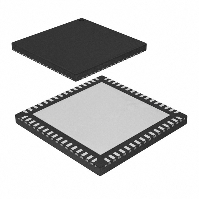


 工商网监
湘ICP备2023018690号
工商网监
湘ICP备2023018690号
