SAMA5D27 Wireless SOM1
ATSAMA5D27-WLSOM1
Introduction
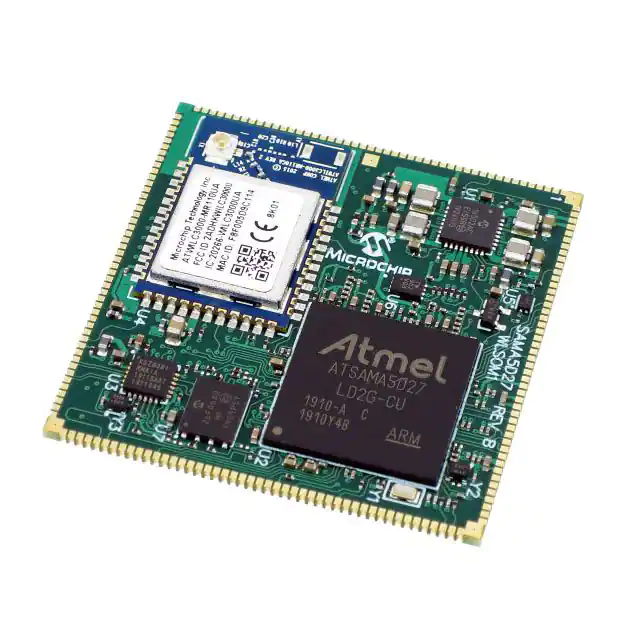
The Microchip SAMA5D27 Wireless System-On-Module 1 (ATSAMA5D27-WLSOM1) is a small single-sided SOM
based on the high-performance System-in-Package (SiP) 32-bit Arm® Cortex®-A5 processor-based MPU
SAMA5D27, 2 Gb LPDDR2 SDRAM running up to 500 MHz, and Wi-Fi® plus Bluetooth® (Wi-Fi/BT) Wireless module.
The ATSAMA5D27-WLSOM1 is built on a common set of proven Microchip components to reduce time to market by
simplifying hardware design and software development.
The ATSAMA5D27-WLSOM1 also limits design rules of the main application board, reducing overall PCB complexity
and cost. The ATSAMA5D27-WLSOM1 is delivered with a free Linux® distribution and bare metal C examples.
Figure 1. ATSAMA5D27-WLSOM1 Overview
© 2019 Microchip Technology Inc.
Datasheet
DS60001590A-page 1
�SAMA5D27 Wireless SOM1
Features
•
•
•
•
•
•
•
•
•
•
•
•
•
•
System-In-Package (ATSAMA5D27C-LD2G-CU) Including:
– Arm® Cortex®-A5 processor-based SAMA5D27 MPU
– 2 Gbit LPDDR2 SDRAM
On-Board Power Management Unit (MCP16502AC-E/S8B)
64 Mb Serial Quad I/O Flash Memory (SST26VF064BEUIT-104I/MF) with Embedded EUI-48™ and EUI-64™
MAC Addresses
IEEE® 802.11 b/g/n Wi-Fi plus Bluetooth (Wi-Fi/BT) Module (ATWILC3000-MR110UA)
10Base-T/100Base-TX Ethernet PHY (KSZ8081RNAIA)
ATECC608A Secure Element
MEMS Oscillators for Clock Generation
40.8 x 40.8 mm Module, Pitch 0.8mm, Solderable Manually for Prototyping
94 I/Os
Up to 7 Tamper Pins
One USB Device, one USB Host and one HSIC Interface
Shutdown and Reset Control Pins
Independent Power Supplies Available for Camera Sensor, for SD Card and for Backup Depending on Voltage
Domains
Operational Specifications:
– Main operating voltage: 3.0V to 5.5V ± 5%
– Temperature range: -40°C to 85°C
– Integrated oscillators, internal voltage regulators
– Multiple interfaces and I/Os for easy application development
Applications
•
•
•
•
•
•
Industrial Control and Automation
Smart Appliances
Human Machine Interfaces (HMI)
IoT Gateway
Access Control Panels
Security and Alarm Systems
© 2019 Microchip Technology Inc.
Datasheet
DS60001590A-page 2
�SAMA5D27 Wireless SOM1
Table of Contents
Introduction.....................................................................................................................................................1
Features......................................................................................................................................................... 2
Applications.................................................................................................................................................... 2
1.
Reference Documents............................................................................................................................ 5
2.
Block Diagram.........................................................................................................................................6
3.
Pinout ..................................................................................................................................................... 7
3.1.
3.2.
4.
Functional Description...........................................................................................................................13
4.1.
4.2.
4.3.
4.4.
4.5.
4.6.
4.7.
5.
Absolute Maximum Ratings........................................................................................................38
Recommended Operating Conditions........................................................................................ 38
DC Characteristics..................................................................................................................... 38
Radio Performances...................................................................................................................39
Mechanical Characteristics................................................................................................................... 40
6.1.
6.2.
6.3.
7.
MPU and Memory Subsystem....................................................................................................13
Power Management................................................................................................................... 17
LAN Subsystem..........................................................................................................................22
Voltage Threshold Detector........................................................................................................22
Radio Subsystem....................................................................................................................... 23
External Interfaces and PIO Muxing...........................................................................................24
Antenna...................................................................................................................................... 36
Electrical Characteristics.......................................................................................................................38
5.1.
5.2.
5.3.
5.4.
6.
Pinout Overview........................................................................................................................... 7
Pin List..........................................................................................................................................7
Module Outline Drawings........................................................................................................... 40
Module Land Pattern (Host Board PCB Footprint)..................................................................... 42
Other Characteristics..................................................................................................................43
Assembly and Storage Information....................................................................................................... 44
7.1.
7.2.
7.3.
7.4.
7.5.
Storage Condition.......................................................................................................................44
Motherboard Solder Paste......................................................................................................... 44
Motherboard Stencil Design....................................................................................................... 44
Bake Information........................................................................................................................ 44
Reflow Profile............................................................................................................................. 45
8.
Regulatory Approval..............................................................................................................................47
9.
Ordering Information............................................................................................................................. 48
10. Revision History.................................................................................................................................... 49
10.1. Rev. A - 10/2019.........................................................................................................................49
The Microchip Web Site............................................................................................................................... 50
© 2019 Microchip Technology Inc.
Datasheet
DS60001590A-page 3
�SAMA5D27 Wireless SOM1
Customer Change Notification Service........................................................................................................ 50
Customer Support........................................................................................................................................ 50
Product Identification System.......................................................................................................................51
Microchip Devices Code Protection Feature................................................................................................ 51
Legal Notice................................................................................................................................................. 51
Trademarks.................................................................................................................................................. 52
Quality Management System Certified by DNV........................................................................................... 52
Worldwide Sales and Service.......................................................................................................................53
© 2019 Microchip Technology Inc.
Datasheet
DS60001590A-page 4
�SAMA5D27 Wireless SOM1
Reference Documents
1.
Reference Documents
The following reference data sheets are available on www.microchip.com:
Table 1-1. Reference Data Sheets
Document Title
Available
KSZ8081RNA/RND
https://www.microchip.com/wwwproducts/en/KSZ8081
SAMA5D2 SIP
https://www.microchip.com/wwwproducts/en/ATSAMA5D27C-LD2G
SST26VF064BEUI
https://www.microchip.com/wwwproducts/en/SST26VF064BEUI
MCP16502
https://www.microchip.com/wwwproducts/en/MCP16502
MIC841/2
https://www.microchip.com/wwwproducts/en/MIC842
DSC60XXB
https://www.microchip.com/wwwproducts/en/DSC6000B
DSC61XXB
https://www.microchip.com/wwwproducts/en/DSC6100B
ATWILC3000-MR110UA
https://www.microchip.com/wwwproducts/en/ATWILC3000
ATECC608A
https://www.microchip.com/wwwproducts/en/ATECC608A
© 2019 Microchip Technology Inc.
Datasheet
DS60001590A-page 5
�SAMA5D27 Wireless SOM1
Block Diagram
Block Diagram
The following figure shows the block diagram of the ATSAMA5D27-WLSOM1 module.
Figure 2-1. ATSAMA5D27-WLSOM1 Module Block Diagram
VDDISC
MAIN
3.0-5.5V
With MAC Address
EUI-48 & EUI-64 Node Identity
CryptoAuthentication™ ECC608A-TNGTLS
24 MHz/DSC6003
RXD
64 Mbit Serial Quad I/O
Flash Memory
SST26VF064BEUIT-104I/MF
DEBUG
BACKUP
WAKEUP
RESET
SHUTDOWN
nSTART_SOM
SYSTEM
CLK_AUDIO
COMPP / COMPN
MISC
MPU
+
2 Gb LPDDR2
SAMA5D27C-LD2G-CU
2 * USB
QSPI_CS
10/100
Ethernet RMII PHY
KSZ8081RNAIA
WiFi / BT Module
32 kHz Crystal
7 * PIOBU
1.8V
900mA
Power Management Unit
MCP16502AC-E/S8B
VLDO2
300mA
Disable Boot
3.3V
600mA
VDDBU
Voltage Monitor MIC842NYMT
VDD
SDHC
JTAG & DBGU Interfaces
VDDANA
25 MHz/DSC6102
VDDFUSE
ATWILC3000
-MR110UA
© 2019 Microchip Technology Inc.
Datasheet
64 Channels Touch
Up to 6 ADC Inputs
CAN Interface
I²S Interface
Mono PDMIC Interface
SSC Interface
CLASS-D Mono
Camera Interface
18-bit LCD Interface
4 FLEXCOM Interfaces
2 SPI Interfaces
5 UART Interfaces
TWI Interface
SD-CARD Interface
SMC 8-bit Interface
2 WILC OUTPUT LEDS
eMMC Interface
Up to 94 Mixable I/O
2 QSPI Interfaces
2.
DS60001590A-page 6
�SAMA5D27 Wireless SOM1
Pinout
3.
Pinout
3.1
Pinout Overview
188 - GND
187 - WKUP
186 - VDD_DDR
185 - VDD_DDR
184 - GND
183 - GND
182 - nSTART_SOM
181 - GND
180 - VLDO2
179 - GND
178 - VTH
177 - PC7
176 - PC6
175 - PA13
174 - PA11
173 - PA7
172 - PA9
171 - PA6
170 - PA12
169 - PA4
168 - PA10
167 - PA8
166 - PA2
165 - PA0
164 - PA3
163 - PA5
162 - PA1
161 - VDDFUSE
160 - GND
159 - VDDANA
158 - GND
157 - HSIC_STROBE
156 - HSIC_DATA
155 - GND
154 - USBB_P
153 - USBB_N
152 - USBA_P
151 - USBA_N
150 - VDDSDHC
149 - GND
148 - PIOBU6
147 - PIOBU4
146 - PIOBU1
145 - CLK_AUDIO
144 - GND
143 - VDDBU
142 - GND
Figure 3-1. ATSAMA5D27-WLSOM1 Pin Assignment
141 - GND
140 - COMPN
139 - COMPP
138 - PIOBU5
137 - PIOBU3
136 - PIOBU7
135 - PIOBU2
134 - RXD
133 - GND
132 - PD25
131 - PD29
130 - PD30
129 - GND
128 - GND
127 - PD26
126 - GND
125 - GND
124 - PD28
123 - PD27
122 - TWCK_SOM_PD20
121 - GND
120 - TWD_SOM_PD19
119 - PD12
118 - PD11
117 - PD14
116 - PD13
115 - PD16
114 - PD15
113 - PD18
112 - PD17
111 - PD10
110 - PD9
109 - PD5
108 - PD8
107 - PD7
106 - PD6
105 - PD4
104 - PD3
103 - PD2
102 - QSPI1_CS_PB6
101 - NCS_QSPI
100 - SIO2_QSPI_PB9
99 - SIO1_QSPI_PB8
98 - SIO0_QSPI_PB7
97 - SIO3_QSPI_PB10
96 - SCK_QSPI_PB5
95 - GND
GND - 48
GND - 49
GND - 50
GND - 51
GND - 52
GND - 53
GND - 54
GND - 55
PC18 - 56
PC16 - 57
PC20 - 58
PC23 - 59
PC10 - 60
PC25 - 61
PC14 - 62
PC21 - 63
PC13 - 64
PC22 - 65
PC24 - 66
PC12 - 67
PC11 - 68
PC9 - 69
PC19 - 70
PC15 - 71
PC17 - 72
VDDISC - 73
GND - 74
PA31 - 75
PA30 - 76
PB4 - 77
PB3 - 78
PB2 - 79
PB1 - 80
PB0 - 81
GND - 82
NC_3-WILC - 83
ETH_LED0 - 84
GND - 85
ETH_RX_N - 86
ETH_RX_P - 87
ETH_TX_N - 88
ETH_TX_P - 89
GND - 90
PB12 - 91
PB11 - 92
GND - 93
GND - 94
GND - 1
VDD_MAIN - 2
VDD_MAIN - 3
VDD_MAIN - 4
GND - 5
GND - 6
NRST - 7
GND - 8
GND - 9
SHDN - 10
GND - 11
VDD_3V3 - 12
VDD_3V3 - 13
GND - 14
PC0 - 15
PC3 - 16
PC2 - 17
PC1 - 18
PC4 - 19
PC5 - 20
PA14 - 21
PA15 - 22
PA16 - 23
PA17 - 24
PB27 - 25
PB31 - 26
PB29 - 27
PB28 - 28
PB26 - 29
PB30 - 30
GND - 31
PD1 - 32
PD0 - 33
PC30 - 34
PC27 - 35
PC31 - 36
PC26 - 37
PC29 - 38
PC28 - 39
GND - 40
NC_20-WILC - 41
RXD_WILC_DBG - 42
TXD_WILC_DBG - 43
GND - 44
GND - 45
GND - 46
GND - 47
3.2
Pin List
The following tables provide the SAMA5D27-WLSOM1 module pin description.
© 2019 Microchip Technology Inc.
Datasheet
DS60001590A-page 7
�SAMA5D27 Wireless SOM1
Pinout
Table 3-1. Pin Description: PIOA
Pin #
Pin Name
Power Rail
Description
165
PA0
VDDSDHC
Configurable GPIO PA0
162
PA1
VDDSDHC
Configurable GPIO PA1
166
PA2
VDDSDHC
Configurable GPIO PA2
164
PA3
VDDSDHC
Configurable GPIO PA3
169
PA4
VDDSDHC
Configurable GPIO PA4
163
PA5
VDDSDHC
Configurable GPIO PA5
171
PA6
VDDSDHC
Configurable GPIO PA6
173
PA7
VDDSDHC
Configurable GPIO PA7
167
PA8
VDDSDHC
Configurable GPIO PA8
172
PA9
VDDSDHC
Configurable GPIO PA9
168
PA10
VDDSDHC
Configurable GPIO PA10
174
PA11
VDD_3V3
Configurable GPIO PA11
170
PA12
VDD_3V3
Configurable GPIO PA12
175
PA13
VDD_3V3
Configurable GPIO PA13
21
PA14
VDD_3V3
Configurable GPIO PA14
22
PA15
VDD_3V3
Configurable GPIO PA15
23
PA16
VDD_3V3
Configurable GPIO PA16
24
PA17
VDD_3V3
Configurable GPIO PA17
76
PA30
VDD_3V3
Configurable GPIO PA30
75
PA31
VDD_3V3
Configurable GPIO PA31
Table 3-2. Pin Description: PIOB
Pin #
Pin Name
Power Rail
Description
81
PB0
VDD_3V3
Configurable GPIO PB0
80
PB1
VDD_3V3
Configurable GPIO PB1
79
PB2
VDD_3V3
Configurable GPIO PB2
78
PB3
VDD_3V3
Configurable GPIO PB3
77
PB4
VDD_3V3
Configurable GPIO PB4
96
SCK_QSPI_PB5
VDD_3V3
QSPI Serial Clock
102
QSPI1_CS_PB6
VDD_3V3
QSPI Chip Select Output Control
98
SIO0_QSPI_PB7
VDD_3V3
QSPI Serial Data Input/Output 0
99
SIO1_QSPI_PB8
VDD_3V3
QSPI Serial Data Input/Output 1
100
SIO2_QSPI_PB9
VDD_3V3
QSPI Serial Data Input/Output 2
97
SIO3_QSPI_PB10
VDD_3V3
QSPI Serial Data Input/Output 3
92
PB11
VDD_3V3
Configurable GPIO PB11
© 2019 Microchip Technology Inc.
Datasheet
DS60001590A-page 8
�SAMA5D27 Wireless SOM1
Pinout
...........continued
Pin #
Pin Name
Power Rail
Description
91
PB12
VDD_3V3
Configurable GPIO PB12
29
PB26
VDD_3V3
Configurable GPIO PB26
25
PB27
VDD_3V3
Configurable GPIO PB27
28
PB28
VDD_3V3
Configurable GPIO PB28
27
PB29
VDD_3V3
Configurable GPIO PB29
30
PB30
VDD_3V3
Configurable GPIO PB30
26
PB31
VDD_3V3
Configurable GPIO PB31
Table 3-3. Pin Description: PIOC
Pin #
Pin Name
Power Rail
Description
15
PC0
VDD_3V3
Configurable GPIO PC0
18
PC1
VDD_3V3
Configurable GPIO PC1
17
PC2
VDD_3V3
Configurable GPIO PC2
16
PC3
VDD_3V3
Configurable GPIO PC3
19
PC4
VDD_3V3
Configurable GPIO PC4
20
PC5
VDD_3V3
Configurable GPIO PC5
176
PC6
VDD_3V3
Configurable GPIO PC6
177
PC7
VDD_3V3
Configurable GPIO PC7
69
PC9
VDDISC
Configurable GPIO PC9
60
PC10
VDDISC
Configurable GPIO PC10
68
PC11
VDDISC
Configurable GPIO PC11
67
PC12
VDDISC
Configurable GPIO PC12
64
PC13
VDDISC
Configurable GPIO PC13
62
PC14
VDDISC
Configurable GPIO PC14
71
PC15
VDDISC
Configurable GPIO PC15
57
PC16
VDDISC
Configurable GPIO PC16
72
PC17
VDDISC
Configurable GPIO PC17
56
PC18
VDDISC
Configurable GPIO PC18
70
PC19
VDDISC
Configurable GPIO PC19
58
PC20
VDDISC
Configurable GPIO PC20
63
PC21
VDDISC
Configurable GPIO PC21
65
PC22
VDDISC
Configurable GPIO PC22
59
PC23
VDDISC
Configurable GPIO PC23
66
PC24
VDDISC
Configurable GPIO PC24
61
PC25
VDDISC
Configurable GPIO PC25
© 2019 Microchip Technology Inc.
Datasheet
DS60001590A-page 9
�SAMA5D27 Wireless SOM1
Pinout
...........continued
Pin #
Pin Name
Power Rail
Description
37
PC26
VDD_3V3
Configurable GPIO PC26
35
PC27
VDD_3V3
Configurable GPIO PC27
39
PC28
VDD_3V3
Configurable GPIO PC28
38
PC29
VDD_3V3
Configurable GPIO PC29
34
PC30
VDD_3V3
Configurable GPIO PC30
36
PC31
VDD_3V3
Configurable GPIO PC31
Table 3-4. Pin Description: PIOD
Pin #
Pin Name
Power Rail
Description
33
PD0
VDD_3V3
Configurable GPIO PD0
32
PD1
VDD_3V3
Configurable GPIO PD1
103
PD2
VDD_3V3
Configurable GPIO PD2
104
PD3
VDDANA
Configurable GPIO PD3
105
PD4
VDDANA
Configurable GPIO PD4
109
PD5
VDDANA
Configurable GPIO PD5
106
PD6
VDDANA
Configurable GPIO PD6
107
PD7
VDDANA
Configurable GPIO PD7
108
PD8
VDDANA
Configurable GPIO PD8
110
PD9
VDDANA
Configurable GPIO PD9
111
PD10
VDDANA
Configurable GPIO PD10
118
PD11
VDDANA
Configurable GPIO PD11
119
PD12
VDDANA
Configurable GPIO PD12
116
PD13
VDDANA
Configurable GPIO PD13
117
PD14
VDDANA
Configurable GPIO PD14
114
PD15
VDDANA
Configurable GPIO PD15
115
PD16
VDDANA
Configurable GPIO PD16
112
PD17
VDDANA
Configurable GPIO PD17
113
PD18
VDDANA
Configurable GPIO PD18
120
TWD_SOM_PD19
VDDANA
I²C Data Line
122
TWCK_SOM_PD20
VDDANA
I²C Clock Line
132
PD25
VDDANA
Configurable GPIO PD25
127
PD26
VDDANA
Configurable GPIO PD26
123
PD27
VDDANA
Configurable GPIO PD27
124
PD28
VDDANA
Configurable GPIO PD28
131
PD29
VDDANA
Configurable GPIO PD29
© 2019 Microchip Technology Inc.
Datasheet
DS60001590A-page 10
�SAMA5D27 Wireless SOM1
Pinout
...........continued
Pin #
Pin Name
Power Rail
Description
130
PD30
VDDANA
Configurable GPIO PD30
Table 3-5. Pin Description: System
Pin #
Pin Name
Power Rail
Description
145
CLK_AUDIO
VDD_3V3
Audio Master Clock Frequency Output
151
USBA_N
VDD_3V3
USB Host Port A High-Speed Data -
152
USBA_P
VDD_3V3
USB Host Port A High-Speed Data +
157
HSIC_STROBE
VDDHSIC (1.2V)
USB High-Speed Inter-Chip Strobe
156
HSIC_DATA
VDDHSIC (1.2V)
USB High-Speed Inter-Chip Data
153
USBB_N
VDD_3V3
USB Host Port B High-Speed Data -
154
USBB_P
VDD_3V3
USB Host Port B High-Speed Data +
7
NRST
VDDBU
Module Reset
140
COMPN
VDDBU
External Analog Data Input
139
COMPP
VDDBU
External Analog Data Input
146
PIOBU1
VDDBU
Tamper I/O #1
135
PIOBU2
VDDBU
Tamper I/O #2
137
PIOBU3
VDDBU
Tamper I/O #3
147
PIOBU4
VDDBU
Tamper I/O #4
138
PIOBU5
VDDBU
Tamper I/O #5
148
PIOBU6
VDDBU
Tamper I/O #6
136
PIOBU7
VDDBU
Tamper I/O #7
134
RXD
VDDBU
RXLP Receive Data Input
10
SHDN
VDDBU
Shutdown Control
187
WKUP
VDDBU
Module Wake-Up
178
VTH
VDD_MAIN
Low Voltage Threshold Detection Input
101
NCS_QSPI
VDD_3V3
Embedded QSPI Chip Select Input
83
NC
–
Not connected
41
NC
–
Not connected
89
ETH_TX_P
–
Physical Transmit Signal (+ differential)
88
ETH_TX_N
–
Physical Transmit Signal (– differential)
87
ETH_RX_P
–
Physical Receive Signal (+ differential)
86
ETH_RX_N
–
Physical Receive Signal (– differential)
84
ETH_LED0
VDD_3V3
Programmable LED0 Output
182
nSTART_SOM
VDD_MAIN
Module Start-up Control Input
42
RXD_WILC_DBG
VDD_3V3
Used for Radio Debug. UART RXD
© 2019 Microchip Technology Inc.
Datasheet
DS60001590A-page 11
�SAMA5D27 Wireless SOM1
Pinout
...........continued
Pin #
Pin Name
Power Rail
Description
43
TXD_WILC_DBG
VDD_3V3
Used for Radio Debug. UART TXD
Table 3-6. Pin Description: Power
Pin #
Pin Name
1, 5, 6, 8, 9, 11, 14, 31, 40, 44, 45, 46, 47, 48, 49, 50,
51, 52, 53, 54, 55, 74, 82, 85, 90, 93, 94, 95, 121, 125,
126, 129, 133, 141, 142, 144, 128, 149, 155, 158, 160,
179, 181, 183, 184, 188
GND
GND
GND
Ground
159
VDDANA
VDDANA
I
Analog Voltage Input
143
VDDBU
VDDBU
I
Backup Voltage Input
161
VDDFUSE
VDDFUSE
I
VDDFUSE Voltage Input
73
VDDISC
VDDISC
I
VDDISC Voltage Input
I
Main input Voltage
2, 3, 4
Power Rail Type
VDD_MAIN VDD_MAIN
Description
12, 13
VDD_3V3
VDD_3V3
O
3.3V Voltage Output
180
VLDO2
VLDO2
O
VLDO2 Output Voltage
VDDSDHC VDDSDHC
I
VDDSDHC Input Voltage
VDD_DDR
O
1.8V Output Voltage
150
185, 186
© 2019 Microchip Technology Inc.
Datasheet
VDD_DDR
DS60001590A-page 12
�SAMA5D27 Wireless SOM1
Functional Description
4.
Functional Description
4.1
MPU and Memory Subsystem
4.1.1
SAMA5D27 System-In-Package
The SAMA5D27 System-In-Package (SiP) (ATSAMA5D27C-LD2G-CU) integrates the ARM Cortex-A5 processorbased SAMA5D2 MPU with 2 Gbit LPDDR2-SDRAM in a single package.
By combining the high-performance, ultra-low power SAMA5D2 with LPDDR2-SDRAM in a single package, PCB
routing complexity, area and number of layers is reduced. This makes board design easier and lowers the overall
cost of the bill of materials. Board design is more robust by facilitating design for EMI, ESD and signal integrity.
For more information about the SiP, refer to 1. Reference Documents. This section lists the sole reference
documents for product information on the SAMA5D2 and the LPDDR2-SDRAM memory.
The ATSAMA5D27C-LD2G-CU is available in a 361-ball TFBGA package.
Connections of the supplies and the system pins of the ATSAMA5D27C-LD2G-CU are described in the following
schematics.
Figure 4-1. SAMA5D27 SiP Schematic
1
PD23
2
24MHz
Y2
OE
OUT
GND VDD
3
XIN_24MHz
VDD_3V3
4
C38
DSC6003HI2B-024.0000
GND
0.1uF
6.3V
0201
GND
XIN_24MHz
U2F SAMA5D27C-LD2G-CU
W5
W7
XIN
HHSDPA
W4
V7
XOUT
HHSDMA
DIFF90
DIFF90
XIN_32KHz
XOUT_32KHz
U1
XIN32
T1
XOUT32
DIFF90
DIFF90
P4
SHDN
U2
WKUP
W3
NRST
Y1
XIN_32KHz
C18
8pF
50V
0201
GND
R1
RXD
XOUT_32KHz
32.768 Hz
6pF
VDDANA
M9
C19
8pF
50V
0201
GND
T3
T2
R11
SHDN
WKUP
NRST
RXD
ADVREFP
JTAGSEL
TST
W8
HHSDPB
V8
HHSDMB
W9
HHSDPDATC
W10
HHSDMSTRC
COMPP
COMPN
R4
R5
R3
T4
U3
T5
U5
P5
PIOBU0_PMIC
PIOBU1
PIOBU2
PIOBU3
PIOBU4
PIOBU5
PIOBU6
PIOBU7
W2
CLK_AUDIO
V6
VBG
CLK_AUDIO
C17
10K
1%
0201
USBB_P
USBB_N
HSIC_DATA
HSIC_STROBE
V1
COMPP
V2
COMPN
PIOBU0
PIOBU1
PIOBU2
PIOBU3
PIOBU4
PIOBU5
PIOBU6
PIOBU7
USBA_P
USBA_N
DNP
10pF
25V
0201
R12
5.62K
0201
1%
GND
GND
© 2019 Microchip Technology Inc.
Datasheet
DS60001590A-page 13
�SAMA5D27 Wireless SOM1
Functional Description
Figure 4-2. SAMA5D27 SiP Decoupling Schematic
VDDIODDR
0402
0402
0402
0201
0201
0201
0201
0201
0201
0201
0201
0201
0201
0201
0201
0201
0201
0201
0201
0201
0201
0201
0201
4.7uF
4.7uF
4.7uF
0.1uF
0.1uF
0.1uF
0.1uF
0.1uF
0.1uF
0.1uF
0.1uF
0.1uF
0.1uF
0.1uF
0.1uF
0.1uF
0.1uF
0.1uF
0.1uF
0.1uF
0.1uF
0.1uF
0.1uF
C21
C23
C25
C27
C29
C31
C33
C35
C37
C39
C41
C42
C44
C45
C47
C49
C50
C52
C54
C55
C56
C58
C59
0201
0201
0402
0402
0201
0201
0201
0201
0201
0201
0.1uF
0.1uF
4.7uF
4.7uF
0.1uF
0.1uF
0.1uF
0.1uF
0.1uF
0.1uF
C61
C62
C64
C65
C67
C68
C70
C71
C73
C74
0201 0.1uF
C76
0201 0.1uF
C78
0201 0.1uF
C80
0402 4.7uF
C82
DDR_VREF
VDDIODDR
VDD_DDR
B15
B17
B19
D15
D17
D19
F15
F17
F19
H15
H17
H19
K15
K17
K19
M15
M17
M19
P15
P17
P19
T17
T19
U2E
SAMA5D27C-LD2G-CU
DDRM_VDD12
DDRM_VDD12
DDRM_VDD12
DDRM_VDD12
DDRM_VDD12
DDRM_VDD12
DDRM_VDD12
DDRM_VDD12
DDRM_VDD12
DDRM_VDD12
DDRM_VDD12
DDRM_VDD12
DDRM_VDD12
DDRM_VDD12
DDRM_VDD12
DDRM_VDD12
DDRM_VDD12
DDRM_VDD12
DDRM_VDD12
DDRM_VDD12
DDRM_VDD12
DDRM_VDD12
DDRM_VDD12
M12
DDR_VREF-01
J10
DDR_VREF-02
E8
E11
H10
J8
J13
L10
P12
B11
B13
D11
D13
K13
K16
DDRM_VSS
DDRM_VSS
DDRM_VSS
DDRM_VSS
DDRM_VSS
DDRM_VSS
DDRM_VSS
DDRM_VSS
DDRM_VSS
DDRM_VSS
DDRM_VSS
DDRM_VSS
DDRM_VSS
DDRM_VSS
DDRM_VSS
DDRM_VSS
DDRM_VSS
DDRM_VSS
DDRM_VSS
DDRM_VSS
DDRM_VSS
DDRM_VSS
DDRM_VSS
DDRM_VSS
VDDDDR
VDDDDR
VDDDDR
VDDDDR
VDDDDR
VDDDDR
VDDDDR
GNDDDR
GNDDDR
GNDDDR
GNDDDR
GNDDDR
GNDDDR
GNDDDR
DDRM_VDD18
DDRM_VDD18
DDRM_VDD18
DDRM_VDD18
DDRM_VDD18
DDRM_VDD18
GND
GND
E10
F8
G10
J9
L11
M13
N12
VDDISC
C99
4.7uF
10V
0402
GND
ZQ
C19 R19
0201
GND
240R
1%
GND
GND
4.1.2
4.7uF
4.7uF
0.1uF
0.1uF
0.1uF
0.1uF
0.1uF
0.1uF
0.1uF
C20
C22
C24
C26
C28
C30
C32
C34
C36
0201 0.1uF
C40
0201 0.1uF
C43
0201 0.1uF
0201 0.1uF
C46
C48
0201 0.1uF
0201 0.1uF
C51
C53
0402
0402
0201
0201
0201
0201
0201
0201
0201
A14
A19
B14
B18
C14
C18
D14
D18
E14
E18
F14
F18
G14
G18
H14
H18
N14
N17
N18
P14
P18
R14
R18
T18
VDDCORE
VDDFUSE
VDDCORE
U2G
C3
C9
K3
U9
W6
V5
K8
U15
U7
VDD_3V3
SAMA5D27C-LD2G-CU
VDDCORE
VDDCORE
VDDCORE
VDDCORE
VDDCORE
VDDCORE
VDDCORE-04
GNDCORE
GNDCORE
GNDCORE
GNDCORE
GNDCORE
GNDCORE
GNDCORE
VDDFUSE
GNDDPLL
C57
VDDIODDR
B4
VDDIOP0
D5
VDDIOP0
0201 0.1uF
0402 4.7uF
0201 0.1uF
C60
C101
C63
0201 0.1uF
C66
0201 0.1uF
C69
0201 0.1uF
C72
0201 0.1uF
C75
0201 0.1uF
C77
0201 0.1uF
C79
0201 0.1uF
C81
0201 0.1uF
C83
0201 10nF
C100
A8
VDDANA
G1
H6
VDDBU
V3
VDDISC
G3
VDDOSC_PLL
R6
VDDUTMII
R8
VDDCORE
VDDOSC_PLL
VDDPLLA
T6
R10
VDDSDHC
P9
T7
N9
VDDHSIC
VDDIOP2
GNDIOP1
GNDIOP1
GNDIOP1
GNDIOP1
GNDIOP2
VDDANA
GNDANA
VDDANA
GNDANA
VDDBU
GNDBU
VDDISC
GNDISC
VDDAUDIOPLL
GNDAUDIOPLL
VDDUTMI
VDDUTMI_CORE
DDR_VREF (0V6)
D4
GNDIOP0
A5
GNDIOP0
V13
VDDIOP1
V18
VDDIOP1
0201 0.1uF
A1
D9
K4
K7
J11
W1
V9
GNDUTMI
GNDUTMI_CORE
VDDOSC
GNDOSC
VDDPLLA
GNDPLLA
VDDSDMMC
GNDSDMMC
C11
W13
W19
R13
P13
B9
C12
4.7uF
10V
0402
F1
0.1uF
6.3V
0201
C16
0.1uF
6.3V
0201
G5
R9
1.5k
0402
1%
R10
1.5k
0402
1%
U4
GND
H3
GND
P6
R7
U6
T11
P10
T8
C100
4.7uF
10V
0402
GND
GND
Power Management Unit
The MCP16502 is a full-featured PMIC optimized for Microchip MPU devices.
The MCP16502 integrates four DC-DC buck regulators and two auxiliary LDOs, and provides a comprehensive
interface to the MPU, which includes an Interrupt flag and an I2C interface.
All buck channels can support loads up to 1A. All bucks are 100% duty cycle capable.
Two 300mA LDOs are provided such that sensitive analog loads can be supported.
The default power channel sequencing is built-in, according to the requirements of the Microchip MPU device.
The MCP16502 features a low no-load operational quiescent current, and it draws less than 10 uA in full shutdown.
Active discharge resistors are provided on each output. All buck channels support safe start-up into pre-biased
outputs.
The MCP16502 is available in a 32-pin 5 mm x 5 mm VQFN package with an operating junction temperature range
from –40°C to +125°C. It is AEC-Q100 Grade 2 (TAMB=105°C) qualified.
© 2019 Microchip Technology Inc.
Datasheet
DS60001590A-page 14
�SAMA5D27 Wireless SOM1
Functional Description
Figure 4-3. Power Management Unit Schematic
VDD_MAIN
R1
100k
0201
3
1
PIOBU0_PMIC
2
Q1
BSS138
LPM
GND
GND
R2
10K
1%
1k
1%
0201
R3
SHDN
0201
22
23
8
24
nSTART_SOM
U1
LPM
MCP16502AC-E/S8B
10
PVIN1
PWRHLD
nSTRT
PGND1
17
10K
1%
0201
INT_MCP16502_PC8
SELV2
R5
0R
0201
R6
GND
1
7
WKUP
5
TWD_MCP16502_PD19
6
TWCK_MCP16502_PD20
PGND2
nINTO
nRSTO
nSTRTO
PVIN3
PGND3
VDD_MAIN
18
SELVL1
PGND4
C10
4.7uF
10V
0402
4
SVIN
LVIN
LOUT1
3
33
SGND
LOUT2
EP
GND
VDDUTMII (3V3)
180R
C97
BLM18PG181SN1D
4.7uF
10V
0402
VDD_3V3
max 1A
R4
2.2R
5%
0201
L2
10uH
GND
4.7uF
10V
0402
C4
4.7uF
10V
0402
VDDOSC_PLL (3V3)
C3
MLZ1608N100LT000
VDD_MAIN
GND
C5
GND
22uF
10V
0603
L3
1.5uH
DFE252012P-1R5M=P2
VDDIODDR (1V2)
max 1A
VDD_MAIN
C6
4.7uF
10V
0402
28
C7
GND
22uF
10V
0603
L4
1.5uH
DFE252012P-1R5M=P2
VDD_MAIN
31
C8
4.7uF
10V
0402
29
30
SW4
32
OUT4
VDD_MAIN
22uF
10V
0603
L1
26
27
SW3
25
OUT3
PVIN4
GND
1.5uH
DFE252012P-1R5M=P2
13
SDA
SCL
C2
15
14
SW2
16
OUT2
2
NRST
4.7uF
10V
0402
12
11
SW1
9
OUT1
FB1
C1
HPM
PVIN2
VDD_3V3
VDD_MAIN
max 1A
R8
0201
2.2R
5%
GND
22uF
10V
0603
L6
(1V25)
VDDPLLA
(1V25)
VDD_DDR
(1V8)
VLDO1
(3V3)
VLDO2
(1.8V - 3V3)
L5
10uH
MLZ1608N100LT000
C98
4.7uF
10V
0402
C9
1.5uH
DFE252012P-1R5M=P2
VDDCORE
max 1A
GND
VDD_MAIN
20
max 0.3A
19
max 0.3A
21
C13
C14
4.7uF
10V
0402
4.7uF
10V
0402
C15
4.7uF
10V
0402
GND
4.1.3
SQI Memory
4.1.3.1
Description and Schematic
The ATSAMA5D27-WLSOM1 embeds the SST26VF064BEUIT-104I/MF, a 64 Mb Serial Quad I/O Flash memory.
The SST26VF064BEUIT-104I/MF SQI features a six-wire, 4-bit I/O interface that allows for low-power, highperformance operation in a low pin-count package.
The SST26VF064BEUIT-104I/MF also embeds EUI-48 and EUI-64 MAC addresses.
The SST26VF064BEUIT-104I/MF is available in 8-lead WDFN package with 6 mm × 5 mm dimensions.
For more information, refer to the product web page.
It is possible to deselect the Chip Enable of the embedded QSPI to use external one. In this case, the NCS_QSPI pin
must be left floating and the signal QSPI1_CS_PB6 must be connected to an external QSPI Chip Select.
© 2019 Microchip Technology Inc.
Datasheet
DS60001590A-page 15
�SAMA5D27 Wireless SOM1
Functional Description
Figure 4-4. QSPI Memory Schematic
VDD_3V3
R36
R37
R38
R39
R40
R41
10K
10K
10K
10K
10K
10K
DNP
DNP
DNP
DNP
DNP
1%
0201
0201
0201
0201
0201
0201
R44
R45
R46
R47
R48
QSPI1_IO0_PB7
QSPI1_IO1_PB8
QSPI1_IO2_PB9
QSPI1_IO3_PB10
QSPI1_SCK_PB5
22R
22R
22R
22R
22R
5
2
3
7
6
1
VDD_3V3
U7
SI/SIO0
SO/SIO1
WP/SIO2
HOLD/SIO3
SCK
CE
VDD
8
C96
0.1uF
6.3V
0201
4
VSS
9
TPAD
SST26VF064BEUIT-104I/MF
R49
R50
R51
R52
R53
4.1.3.2
22R
22R
22R
22R
22R
GND
SCK_QSPI_PB5
SIO3_QSPI_PB10
SIO2_QSPI_PB9
SIO1_QSPI_PB8
SIO0_QSPI_PB7
NCS_QSPI
MAC Address
The SST26VF064BEUI is pre-programmed at the factory with globally unique EUI-48 and EUI-64 node identifiers.
The addresses are located in the Serial Flash Discoverable Parameters (SFDP) table and accessible via the SFDP
read instruction.
The 6-byte EUI-48 address value of the SST26VF064BEUI is stored in the SFDP table at address locations 0x261
through 0x266.
The 8-byte EUI-64 address value of the SST26VF064BEUI is stored in the SFDP table at address locations 0x268
through 0x26F.
For more information, refer to the product web page.
Secure Element
The ATECC608A is a member of the Microchip CryptoAuthentication™ family of high-security cryptographic devices
which combine world-class hardware-based key storage with hardware cryptographic accelerators to implement
various authentication and encryption protocols.
The ATECC608A has a flexible command set that allows use in many applications, including Network/IoT Node
Endpoint Security, Secure Boot, Small Message Encryption, Key Generation for Software Download and Ecosystem
control and Anti-Counterfeiting.
Figure 4-5. ECC608A Secure Element Schematic
VDD_3V3
R42
VDD_3V3
0.1uF
6.3V
0201
U6 ATECC608A-TNGTLS
8
3
VCC
NC
1
6
NC
SCL
2
5
NC
SDA
4
7
GND
NC
R43
2.2K
0201
1%
TWCK_ECC608_PD22
TWD_ECC608_PD21
PAD
C95
2.2K
0201
1%
9
4.1.4
GND
GND
© 2019 Microchip Technology Inc.
Datasheet
DS60001590A-page 16
�SAMA5D27 Wireless SOM1
Functional Description
4.2
Power Management
4.2.1
Power Architecture
Basic operation of the ATSAMA5D27-WLSOM1 requires a +5.0V input voltage supply, and a VDDBU (+1.65V to
+3.6V) input voltage supply generally ensured by a backup battery. +5.0V power is supplied to the VDD_MAIN
domain.
CAUTION
As a general design rule, it is recommended to connect all input supply pins, except VDDFUSE which
must be connected to GND by a 100 Ohms resistor if not used, to your power supply and at least a
matching number of ground (GND) pins. For the best EMI performance, it is recommended to connect ALL
ground pins of the ATSAMA5D27-WLSOM1 module to a solid ground plane.
Power-on is controlled through the nSTART_SOM signal. This signal must be provided by the host board, e.g. via an
automated reset controller or a push-button.
The ATSAMA5D27-WLSOM1 module can operate from a single voltage supply (VDD_MAIN) with a value comprised
between +3.0V and +5.5V and, with the MCP16502 PMIC device, internally generates the voltage supplies required
by the SAMA5D2 processor and on-board components.
The PMIC on-board switching regulators generates the 3.3V, 1.20V, 1.25V and 1.8V voltage supplies required by the
SAMA5D27 processor and onboard components.
The ATSAMA5D27-WLSOM1 delivers external power supplies to main board application such as VDD_DDR (1.8V
with 900 mA current capability), VDD_3V3 (3.3V with 600mA output current capability) and VLDO2 output (1.8V to
3.3V with 300 mA output current capability).
Figure 4-6. ATSAMA5D27-WLSOM1 Power Architecture
WILC
3000
Digital
KSZ
8081
SST
26
ECC
608A
DSC
6003
DSC
6102
VDD_3V3
VDDBU
[1.65V .. 3.6V]
Up to 600mA
SAMA5D27C-LD2G-CU
MCP16502AC
VDD_MAIN
[3.0V .. 5.5V]
1
MIC
842
DC/DCs
2
3
4
3.3V
VDDISC
1.2V
VDDANA
VDDFUSE
1.25V
VDDSDMMC
VDDISC
VDDANA
VDDFUSE
VDDSDHC
1.8V
VDD_DDR
2
LDOs
1
1.8 to 3.3V (Off by default)
3.3V
VLDO2
Up to 900mA
Up to 300mA
WILC
3000
PA
ATSAMA5D27-WLSOM1
© 2019 Microchip Technology Inc.
Datasheet
DS60001590A-page 17
�SAMA5D27 Wireless SOM1
Functional Description
4.2.2
Various Power Configurations
Two different configurations are described below, depending on customer use.
•
•
4.2.2.1
Single Supply—ATSAMA5D27-WLSOM1 can be supplied by only one input supply (e.g. 5V AC/DC wall adapter)
and other input supplies can be connected to the internal 3.3V regulator VDD_3V3. All the PIO lines are
supplied at 3.3V.
Multiple Supplies—ATSAMA5D27-WLSOM1 can be supplied by 5V and by a backup battery. Some PIO lines
are supplied by different LDOs for specific applications, such as an ISC camera or a high-speed SD card.
Power Configurations: Single Supply
Figure 4-7. ATSAMA5D27-WLSOM1 Single Supply Connection Example
VDDBU
VDD_3V3
VDDISC
VDDANA
Input Supply
(3.0V - 5.5V)
VDD_MAIN
VDDSDHC
VDDFUSE
Application Fuse
(2.5V)
VDD_DDR
Application Board
(1.8V)
VLDO2
Application Board
(1.8V to 3.3V)
ATSAMA5D27-WLSOM1
© 2019 Microchip Technology Inc.
Datasheet
DS60001590A-page 18
�SAMA5D27 Wireless SOM1
Functional Description
4.2.2.2
Power Configurations: Multiple Supplies
Figure 4-8. ATSAMA5D27-WLSOM1 Multiple Supplies Connection Example
VDDBU
Backup
Battery
VDD_3V3
VDDISC
LDO
(2.5V/2.8V/3.0V)
VDDANA
Input Supply
(3.0V - 5.5V)
VDD_MAIN
VDDSDHC
LDO + Switch
(3.3V/1.8V)
VDDFUSE
Application Fuse
(2.5V)
VDD_DDR
Application Board
(1.8V)
VLDO2
Application Board
(1.8V to 3.3V)
ATSAMA5D27-WLSOM1
4.2.3
Power On/Off Sequences
4.2.3.1
LPDDR2 Power-Off Sequence
The LPDDR2 power-off sequence must be controlled by software to preserve the LPDDR2 device.
In this sequence, the CKE signal should be low during the full period the power rails are powering down.
The power failure can be controlled by the embedded Voltage Supervisor (MIC842) and handled at system level (IRQ
on PD31). The LPDDR2 power-off sequence is applied using the bit LPDDR2_LPDDR3_PWOFF in the MPDDRC
Low-Power register (MPDDRC_LPR).
For more information, refer to the following documents:
•
•
SAMA5D2 Series Data sheet available on https://www.microchip.com/, sections LPDDR2 Power Fail
Management and MPDDRC Low-Power Register
Jedec Standard Low Power Double Data Rate 2 (LPDDR2), JESD209-2B
Note: An uncontrolled power-off sequence can be applied only up to 400 times in the life of an LPDDR2 device.
© 2019 Microchip Technology Inc.
Datasheet
DS60001590A-page 19
�SAMA5D27 Wireless SOM1
Functional Description
4.2.3.2
Power ON/OFF Sequences for Single Supply
Figure 4-9. ATSAMA5D27-WLSOM1 Single Supply Connection: Power-On Sequence
SYSTEM STATUS
OFF
STARTUP
POWER-UP
NRST RELEASED
VDD_MAIN
SYSTEM BOOT
I²C COMMAND
VLDO2 POWER UP
5.0V
nSTART_SOM
a
t1
VDD_3V3
b
VDDBU
VDDANA
t2
VDDISC
VDDSDHC
VDD_DDR
c
t3
NRST
d
PMIC_I2C
e
t4
VLDO2
f
Figure 4-10. ATSAMA5D27-WLSOM1 Single Supply Connection: Power-Off Sequence
SYSTEM STATUS
SYSTEM ON
POWER-OFF REQUEST
VDD_MAIN
NRST ASSERTS
SYSTEM OFF
5.0V
SHDN
a
t2
VDD_3V3
b
VDDBU
VDDANA
VDDISC
VDDSDHC
VDD_DDR
c
t3
NRST
d
PMIC_I2C
e
t1
VLDO2
f
Table 4-1. ATSAMA5D27-WLSOM1 Simple Supply Timing Table
Symbol
Description
Min.
Typ.
Max.
Unit
0.5
–
2000
ms
t1
Power-Up Request Timing
t2
VDD_DDR Power-Up Timing
–
8
–
ms
t3
NRST Timing for Release
–
16
–
ms
t4
VLDO2 Power-Up Timing after I²C Request
–
0.5
1
ms
t5
VLDO2 Power-Down Timing after I²C Request
–
–
1
ms
t6
VDD_3V3 Power-Down Timing
–
10
–
µs
t7
NRST Forced to Low Timing
–
–
10
µs
© 2019 Microchip Technology Inc.
Datasheet
DS60001590A-page 20
�SAMA5D27 Wireless SOM1
Functional Description
4.2.3.3
Power ON/OFF Sequences for Multiple Supplies
Figure 4-11. ATSAMA5D27-WLSOM1 Multiple Supplies Connections: Power-On Sequence
SYSTEM STATUS
BACKUP
STARTUP
POWER-UP
NRST RELEASED
VDDBU
SYSTEM BOOT
I²C COMMAND
VLDO2 POWER UP
1.65V TO 3.6V
VDD_MAIN
5.0V
nSTART_SOM
a
t1
VDD_3V3
b
t2
VDDANA
VDDSDHC
t4
c
3.3V
t3
VDDISC
1.8V
d
VDD_DDR
e
t5
NRST
f
PMIC_I2C
g
t6
VLDO2
h
Figure 4-12. ATSAMA5D27-WLSOM1 Multiple Supplies Connections: Power-Off Sequence
SYSTEM STATUS
SYSTEM ON
POWER-OFF REQUEST
NRST ASSERTS
VDD_MAIN
SYSTEM OFF
5.0V
VDDBU
1.65V to 3.6V
SHDN
a
t8
VDD_3V3
b
VDDANA
VDDISC
VDDSDHC
VDD_DDR
c
t9
NRST
d
PMIC_I2C
e
t7
VLDO2
f
Table 4-2. ATSAMA5D27-WLSOM1 Multiple Supplies Timing Table
Symbol
4.2.4
Description
Min.
Typ.
Max.
Unit
0.5
–
2000
ms
t1
Power-Up Request Timing
t2
VDDSDHC Power-Up Timing
–
35
100
µs
t3
VDDISC Power-Up Timing
–
40
100
µs
t4
VDD_DDR Power-Up Timing
–
8
–
ms
t5
NRST Timing for Release
–
16
–
ms
t6
VLDO2 Power-Up Timing after I²C Request
–
0.5
1
ms
t7
VLDO2 Power-Down Timing after I²C Request
–
–
1
ms
t8
VDD_3V3 Power-Down Timing
–
10
–
µs
t9
NRST Forced to Low Timing
–
–
10
µs
Baseboard Power Delivery Application Diagram Example
The following figure is an example of power architecture at the baseboard level, input to the SOM and output from the
SOM.
© 2019 Microchip Technology Inc.
Datasheet
DS60001590A-page 21
�SAMA5D27 Wireless SOM1
Functional Description
Figure 4-13. Baseboard Power Delivery Application Diagram Example
DCIN
LDO
REGULATOR
MIC5353YMT
DC/DC
CONVERTER
(12V)
(3.3V / 1.8V)
(3.3V)
VDDSDHC
SD-CARD
VDD_3V3
VDDANA
(5.0V)
VDDIN
MIC24051
1V8 Output
SHDN
LDO
REGULATOR
VLDO2
VDDISC
(2.5V)
(1.8V-3.3V)
CAMERA
MIC5259-2.5YD5
WLSOM1
SuperCap
Charger
(Discret Comp.)
SuperCap
5.5V
LDO
REGULATOR
MCP1810T-18
VDDBU
GND
4.3
LAN Subsystem
4.3.1
Ethernet Phy
The Microchip ATSAMA5D27-WLSOM1 embeds a single-supply 10Base-T/100Base-TX Ethernet physical layer
transceiver for transmission and reception of data over a standard CAT-5 unshielded twisted pair (UTP) cable.
The KSZ8081RNAIA is a highly-integrated PHY solution. The KSZ8081RNAIA offers the Reduced Media
Independent Interface (RMII) for direct connection to RMII-compliant MACs in Ethernet processors.
The KSZ8081RNAIA is available in 24-pin, lead-free QFN packages. For more information, refer to the product web
page.
Figure 4-14. Ethernet Phy Schematic
VDD_3V3
R20
R21
1k
0201
U3
ETH_TX_P
ETH_TX_N
ETH_RX_P
ETH_RX_N
DIFF100
DIFF100
6
TXP
5
TXM
DIFF100
DIFF100
4
RXP
3
RXM
0402 10V 2.2uF
0201 0.1uF
6.3V
R22
C84
C85
6.49K
1%
0201
1
VDD_1V2
22
GND
25
PADDLE
9
REXT
KSZ8081RNAIA-TR
REF_CLK
TXD1
TXD0
TXEN
RXD1
RXD0
RXER
CRS_DV/PHYAD[1_0]
MDC
MDIO
INTRP
VDDA_3V3
16
21
20
19
12
13
17
15
11
10
18
2
PD24
2
Y3
OE
25MHz
OUT
GND VDD
3
4
XIN_25MHz
VDD_3V3
8
XI
VDDIO
14
C86
0.1uF
6.3V
0201
GND
C88
10uF
6.3V
0402
C90
DSC6102HI2B-025.0000
7
XO
GND
4.4
TP10
10uF
6.3V
0402
GND
1
1k
0201
LED0/ANEN_SPEED
RST
FB2
VDD_3V3
R23
C87 BLM18PG181SN1D
0.1uF
6.3V
0201
0.1uF
6.3V
0201
10K
1%
0201
GND
GND
C89
23
24
180R
ETH_GTXCK_PB14
ETH_GTX1_PB21
ETH_GTX0_PB20
ETH_GTXEN_PB15
ETH_GRX1_PB19
ETH_GRX0_PB18
ETH_GRXER_PB17
ETH_GRXDV_PB16
ETH_GMDC_PB22
ETH_GMDIO_PB23
ETH_INT_PB24
R24
GND
10K
1%
0201
ETH_LED0
R25
0R
0201
NRST
Voltage Threshold Detector
The Microchip ATSAMA5D27-WLSOM1 embeds a MIC842 micro-power, precision-voltage comparator with an onchip voltage reference.
© 2019 Microchip Technology Inc.
Datasheet
DS60001590A-page 22
�SAMA5D27 Wireless SOM1
Functional Description
The device is intended for voltage monitoring applications. External resistors are used to set the voltage monitor
threshold. When the threshold is crossed, the outputs switch polarity. Refer to the figures below.
The MIC842 incorporates a voltage reference and comparator with fixed internal hysteresis; two external resistors are
used to set the switching threshold voltage.
Supply current is extremely low (1.5 μA, typical), making it ideal for portable applications.
The MIC842 is supplied in 4-pin 1.2 mm × 1.6 mm Thin DFN package. For more information, refer to the product web
page.
Figure 4-15. Voltage Threshold Detector Schematic
VDD_MAIN
VDDANA
C94
0.1uF
6.3V
0201
R27
100k
0201
GND
0201
INT_MIC842_PD31
EP
VTH
U5 MIC842NYMT-T5
4
1
VDD OUT
3
2
INP
GND
100R
1%
C104
EP
R57
100pF
25V
0201
GND
GND
GND
Figure 4-16. Voltage Threshold Detector Implementation Example
Application Board
WLSOM1 Module
V_SUPPLY
VDD_MAIN
VDDANA
C94
0201
Rext1
0.1uF
6.3V
INT_MIC842_PD31
EP
100R
1%
C104
EP
R57
0201
100k
0201
MIC842NYMT-T5
4
1
VDD OUT
3
2
INP
GND
U5
VTH
R27
GND
100pF
25V
0201
Rext2
GND
GND
GND
GND
Table 4-3. Output Resistor Ladder Values and Input System Supply Example
4.5
System Supply Voltage
VTH Threshold Value
Rext1 Value
Rext2 Value
5V
4.64V
787 kΩ
287 kΩ
12V
11V
787 kΩ
100 kΩ
24V
21.78V
787 kΩ
47.5 kΩ
48V
39.51V
787 kΩ
25.5 kΩ
Radio Subsystem
The ATSAMA5D27-WLSOM1 embeds an ATWILC3000, a single chip IEEE 802.11 b/g/n RF/Baseband/MAC link
controller and Bluetooth 5. The ATWILC1000 connects to Microchip AVR®/SMART MCUs, SMART MPUs, and other
processors with minimal resource requirements with simple SPI/SDIO-to-Wi-Fi and UART-to-Bluetooth interfaces.
The ATWILC3000 supports single stream 1x1 802.11n mode providing tested throughput of up to 46 Mbps UDP & 28
Mbps TCP/IP. The ATWILC3000 features fully integrated Power Amplifier, LNA, Switch and Power Management.
Implemented in low-power CMOS technology, the ATWILC3000 offers very low power consumption while
simultaneously providing high performance and minimal bill of materials.
© 2019 Microchip Technology Inc.
Datasheet
DS60001590A-page 23
�SAMA5D27 Wireless SOM1
Functional Description
The ATWILC3000 utilizes highly optimized 802.11-Bluetooth coexistence protocols. The only external clock sources
needed for the ATWILC3000 is a high-speed crystal or oscillator and a 32.768 kHz clock for sleep operation.
For more information, refer to the product web page.
Figure 4-17. Wi-Fi/BT Radio Subsystem Schematic
FB4
FB3
VLDO1
742792731
742792731
VBAT
VDDIO
0402 100R
0402 100R
C91
C92
47uF
10V
0805
VDD_3V3
C105
0.1uF
6.3V
0201
4.7uF
10V
0402
U4
18
VBAT
12
VDDIO
TXD_WILC_DBG
RXD_WILC_DBG
0.1uF
6.3V
0201
GND
16
17
33
7
19
20
2
INT_WILC_PB25
NRST_WILC_PA27
CE_WILC_PA29
RTC_OUT_PB13
R34
R35
3
4
5
6
C106
10K
1%
0201
10000pF
10V
0201
SD_DAT3/GPIO7
SD_DAT2/SPI_MOSI
SD_DAT1/SPI_SSN
UART_TXD SD_DAT0/SPI_MISO
UART_RXD
SD_CMD/SPI_SCK
SD_CLK/GPIO8
IRQN
RESETN
CHIP_EN
BT_TXD
RTC_CLK
BT_RXD
SDIO/SPI_CFG
BT_RTS
BT_CTS
NC
NC
NC
NC
VDD_3V3
35
34
31
30
29
14
32
15
R28
68K
1%
0201
R29
68K
1%
0201
R30
68K
1%
0201
R31
68K
1%
0201
R32
10K
1%
0201
NC_3-WILC
NC_20-WILC
27
26
25
24
23
22
SDIO_DAT3_WILC_PA21
SDIO_DAT2_WILC_PA20
SDIO_DAT1_WILC_PA19
SDIO_DAT0_WILC_PA18
SDIO_CMD_WILC_PA28
SDIO_CK_WILC_PA22
8
9
10
11
TXD_WILC_PA23
RXD_WILC_PA24
RTS_WILC_PA25
CTS_WILC_PA26
1
13
21
28
36
37
10K
1%
0201
GPIO21
GPIO0
GPIO19
GPIO18
GPIO17
GPIO3
GPIO20
GPIO4
C93
R26
10K
1%
0201
ATWILC3000-MR110UA
GND
GND
GND
GND
GND
PADDLE
VDD_3V3
GND
GND
GND
GND
GND
4.6
External Interfaces and PIO Muxing
4.6.1
PIO Muxing
Table 4-4. PIO Muxing: PIOA
PIO
A
IO set
B
IO set
C
IO set
D
IO set
E
IO set
F
IO set
PA0
SDMMC0_CK
1
QSPI0_SCK
1
–
–
–
–
–
–
D0
2
PA1
SDMMC0_CMD
1
QSPI0_CS
1
–
–
–
–
–
–
D1
2
PA2
SDMMC0_DAT0
1
QSPI0_IO0
1
–
–
–
–
–
–
D2
2
PA3
SDMMC0_DAT1
1
QSPI0_IO1
1
–
–
–
–
–
–
D3
2
PA4
SDMMC0_DAT2
1
QSPI0_IO2
1
–
–
–
–
–
–
D4
2
PA5
SDMMC0_DAT3
1
QSPI0_IO3
1
–
–
–
–
–
–
D5
2
PA6
SDMMC0_DAT4
1
–
–
–
–
TIOA5
1
FLEXCOM2_IO0
1
D6
2
PA7
SDMMC0_DAT5
1
–
–
–
–
TIOB5
1
FLEXCOM2_IO1
1
D7
2
PA8
SDMMC0_DAT6
1
–
–
–
–
TCLK5
1
FLEXCOM2_IO2
1
NWE/NANDWE
2
PA9
SDMMC0_DAT7
1
–
–
–
–
TIOA4
1
FLEXCOM2_IO3
1
NCS3
2
PA10
SDMMC0_RSTN
1
–
–
–
–
TIOB4
1
FLEXCOM2_IO4
1
A21/NANDALE
2
PA11
SDMMC0_VDDSEL
1
–
–
–
–
TCLK4
1
–
–
A22/NANDCLE
2
PA12
SDMMC0_WP
1
IRQ
1
–
–
–
–
–
–
NRD/NANDOE
2
PA13
SDMMC0_CD
1
–
–
–
–
–
–
FLEXCOM3_IO1
1
–
–
PA14
SPI0_SPCK
1
TK1
1
–
–
I2SMCK1
2
FLEXCOM3_IO2
1
–
–
PA15
SPI0_MOSI
1
TF1
1
–
–
I2SCK1
2
FLEXCOM3_IO0
1
–
–
© 2019 Microchip Technology Inc.
Datasheet
DS60001590A-page 24
�SAMA5D27 Wireless SOM1
Functional Description
...........continued
PIO
A
IO set
B
IO set
C
IO set
D
IO set
E
IO set
F
IO set
PA16
SPI0_MISO
1
TD1
1
–
–
I2SWS1
2
FLEXCOM3_IO3
1
–
–
PA17
SPI0_NPCS0
1
–
–
–
–
I2SDI1
2
FLEXCOM3_IO4
1
–
–
PA30
–
–
–
–
SPI0_NPCS0
2
PWMH0
1
–
–
–
–
PA31
–
–
–
–
SPI0_MISO
2
PWML0
1
–
–
–
–
Table 4-5. PIO Muxing: PIOB
PIO
A
IO set
C
IO set
D
IO set
F
IO set
PB00
–
–
SPI0_MOSI
2
PWMH1
1
–
–
PB01
–
–
SPI0_SPCK
2
PWML1
1
CLASSD_R0
1
PB02
–
–
–
–
PWMFI0
1
CLASSD_R1
1
PB03
URXD4
1
IRQ
3
PWMEXTRG0
1
CLASSD_R2
1
PB04
UTXD4
1
FIQ
4
–
–
CLASSD_R3
1
PB05
–
–
–
–
QSPI1_SCK
2
–
–
PB06
–
–
–
–
QSPI1_CS
2
–
–
PB07
–
–
–
–
QSPI1_IO0
2
–
–
PB08
–
–
–
–
QSPI1_IO1
2
–
–
PB09
–
–
–
–
QSPI1_IO2
2
–
–
PB10
–
–
–
–
QSPI1_IO3
2
–
–
PB11
–
–
URXD3
3
PDMIC_DAT0
2
–
–
PB12
–
–
UTXD3
3
PDMIC_CLK0
2
–
–
PB26
–
–
URXD0
1
PDMIC_DAT0
1
ISI_D0
3
PB27
–
–
UTXD0
1
PDMIC_CLK0
1
ISI_D1
3
PB28
–
–
FLEXCOM0_IO0
1
TIOA5
2
ISI_D2
3
PB29
–
–
FLEXCOM0_IO1
1
TIOB5
2
ISI_D3
3
PB30
–
–
FLEXCOM0_IO2
1
TCLK5
2
ISI_D4
3
PB31
–
–
FLEXCOM0_IO3
1
TWD0
1
ISI_D5
3
Table 4-6. PIO Muxing: PIOC
PIO
A
IO set
B
IO set
C
IO set
D
IO set
E
IO set
F
IO set
PC00
–
–
–
–
FLEXCOM0_IO4
1
TWCK0
1
–
–
ISI_D6
3
PC01
–
–
–
–
CANTX0
1
SPI1_SPCK
1
I2SCK0
1
ISI_D7
3
PC02
–
–
–
–
CANRX0
1
SPI1_MOSI
1
I2SMCK0
1
ISI_D8
3
PC03
–
–
–
–
TIOA1
1
SPI1_MISO
1
I2SWS0
1
ISI_D9
3
PC04
–
–
–
–
TIOB1
1
SPI1_NPCS0
1
I2SDI0
1
ISI_PCK
3
PC05
–
–
–
–
TCLK1
1
SPI1_NPCS1
1
I2SDO0
1
ISI_VSYNC
3
PC06
–
–
–
–
–
–
SPI1_NPCS2
1
–
–
ISI_HSYNC
3
PC07
–
–
–
–
–
–
SPI1_NPCS3
1
–
–
ISI_MCK
3
© 2019 Microchip Technology Inc.
Datasheet
DS60001590A-page 25
�SAMA5D27 Wireless SOM1
Functional Description
...........continued
PIO
A
IO set
B
IO set
C
IO set
D
IO set
E
IO set
F
IO set
PC09
FIQ
3
–
–
ISI_D0
1
TIOA4
2
–
–
–
–
PC10
LCDDAT2
2
–
–
ISI_D1
1
TIOB4
2
CANTX0
2
–
–
PC11
LCDDAT3
2
–
–
ISI_D2
1
TCLK4
2
CANRX0
2
A0/NBS0
2
PC12
LCDDAT4
2
–
–
ISI_D3
1
URXD3
1
TK0
2
A1
2
PC13
LCDDAT5
2
–
–
ISI_D4
1
UTXD3
1
TF0
2
A2
2
PC14
LCDDAT6
2
–
–
ISI_D5
1
–
–
TD0
2
A3
2
PC15
LCDDAT7
2
–
–
ISI_D6
1
–
–
RD0
2
A4
2
PC16
LCDDAT10
2
–
–
ISI_D7
1
–
–
RK0
2
A5
2
PC17
LCDDAT11
2
–
–
ISI_D8
1
–
–
RF0
2
A6
2
PC18
LCDDAT12
2
–
–
ISI_D9
1
–
–
FLEXCOM3_IO2
2
A7
2
PC19
LCDDAT13
2
–
–
ISI_D10
1
–
–
FLEXCOM3_IO1
2
A8
2
PC20
LCDDAT14
2
–
–
ISI_D11
1
–
–
FLEXCOM3_IO0
2
A9
2
PC21
LCDDAT15
2
–
–
ISI_PCK
1
–
–
FLEXCOM3_IO3
2
A10
2
PC22
LCDDAT18
2
–
–
ISI_VSYNC
1
–
–
FLEXCOM3_IO4
2
A11
2
PC23
LCDDAT19
2
–
–
ISI_HSYNC
1
–
–
–
–
A12
2
PC24
LCDDAT20
2
–
–
ISI_MCK
1
–
–
–
–
A13
2
PC25
LCDDAT21
2
–
–
ISI_FIELD
1
–
–
–
–
A14
2
PC26
LCDDAT22
2
–
–
–
–
CANTX1
1
–
–
A15
2
PC27
LCDDAT23
2
–
–
PCK1
2
CANRX1
1
–
–
A16
2
PC28
LCDPWM
2
FLEXCOM4_IO0
1
PCK2
1
–
–
–
–
A17
2
PC29
LCDDISP
2
FLEXCOM4_IO1
1
–
–
–
–
–
–
A18
2
PC30
LCDVSYNC
2
FLEXCOM4_IO2
1
–
–
–
–
–
–
A19
2
PC31
LCDHSYNC
2
FLEXCOM4_IO3
1
URXD3
2
–
–
–
–
A20
2
Table 4-7. PIO Muxing: PIOD
PIO
A
IO
set
B
IO
set
C
IO
set
D
IO
set
E
IO
set
F
IO
set
Extra
PD0
LCDPCK
2
FLEXCOM4_IO4
1
UTXD3
2
GTSUCOMP
2
–
–
A23
2
–
PD1
LCDDEN
2
–
–
–
–
GRXCK
2
–
–
A24
2
–
PD2
URXD1
1
–
–
–
–
GTXER
2
ISI_MCK
2
A25
2
–
PD3
UTXD1
1
FIQ
2
–
–
GCRS
2
ISI_D11
2
NWAIT
2
PTC_ROW0
PD4
–
–
URXD2
1
–
–
GCOL
2
ISI_D10
2
NCS0
2
PTC_ROW1
PD5
–
–
UTXD2
1
–
–
GRX2
2
ISI_D9
2
NCS1
2
PTC_ROW2
PD6
TCK
2
PCK1
1
–
–
GRX3
2
ISI_D8
2
NCS2
2
PTC_ROW3
PD7
TDI
2
–
–
–
–
GTX2
2
ISI_D0
2
NWR1/NBS1
2
PTC_ROW4
PD8
TDO
2
–
–
–
–
GTX3
2
ISI_D1
2
NANDRDY
2
PTC_ROW5
PD9
TMS
2
–
–
–
–
GTXCK
2
ISI_D2
2
–
–
PTC_ROW6
© 2019 Microchip Technology Inc.
Datasheet
DS60001590A-page 26
�SAMA5D27 Wireless SOM1
Functional Description
...........continued
PIO
A
IO
set
B
IO
set
C
IO
set
D
IO
set
E
IO
set
F
IO
set
Extra
PD10
NTRST
2
–
–
–
–
GTXEN
2
ISI_D3
2
–
–
PTC_ROW7
PD11
TIOA1
3
PCK2
2
–
–
GRXDV
2
ISI_D4
2
–
–
PTC_COL0
PD12
TIOB1
3
FLEXCOM4_IO0
2
–
–
GRXER
2
ISI_D5
2
–
–
PTC_COL1
PD13
TCLK1
3
FLEXCOM4_IO1
2
–
–
GRX0
2
ISI_D6
2
–
–
PTC_COL2
PD14
TCK
1
FLEXCOM4_IO2
2
–
–
GRX1
2
ISI_D7
2
–
–
PTC_COL3
PD15
TDI
1
FLEXCOM4_IO3
2
–
–
GTX0
2
ISI_PCK
2
–
–
PTC_COL4
PD16
TDO
1
FLEXCOM4_IO4
2
–
–
GTX1
2
ISI_VSYNC
2
–
–
PTC_COL5
PD17
TMS
1
–
–
–
–
GMDC
2
ISI_HSYNC
2
–
–
PTC_COL6
PD18
NTRST
1
–
–
–
–
GMDIO
2
ISI_FIELD
2
–
–
PTC_COL7
PD19
–
–
TWD1
3
–
–
–
–
–
–
–
–
AD0
PD20
–
–
TWCK1
3
–
–
–
–
–
–
–
–
AD1
PD23
–
–
–
–
–
–
–
–
–
–
–
–
AD4
PD24
–
–
–
–
–
–
–
–
–
–
–
–
AD5
PD25
SPI1_SPCK
3
–
–
–
–
–
–
–
–
–
–
AD6
PD26
SPI1_MOSI
3
–
–
FLEXCOM2_IO0
2
–
–
–
–
–
–
AD7
PD27
SPI1_MISO
3
TCK
3
FLEXCOM2_IO1
2
–
–
–
–
–
–
AD8
PD28 SPI1_NPCS0
3
TDI
3
FLEXCOM2_IO2
2
–
–
–
–
–
–
AD9
PD29 SPI1_NPCS1
3
TDO
3
FLEXCOM2_IO3
2
TIOA3
3
–
–
–
–
AD10
PD30 SPI1_NPCS2
3
TMS
3
FLEXCOM2_IO4
2
TIOB3
3
–
–
–
–
AD11
4.6.2
Interfacing with an SD Card
The SD (Secure Digital) Card is a non-volatile memory card format used as mass storage memory in mobile devices.
Secure Digital Multimedia Card (SDMMC) Controller
The ATSAMA5D27-WLSOM1 has one Secure Digital Multimedia Card (SDMMC) interface that supports the
MultiMedia Card (e.MMC) Specification V4.41, the SD Memory Card Specification V3.0, and the SDIO V3.0
specification. It is compliant with the SD Host Controller Standard V3.0 specification.
The SDMMC0 interface can be connected to a standard SD card interface.
SDMMC0 Card Connector
The board features a standard MMC/SD card connector, connected to SDMMC0. The SDMMC0 communication is
based on a 4- or 8-pin interface (clock, command, four or eight data and power lines). It may include a card detection
switch.
The figures below illustrate the implementation for the SDMMC0 interface for a 4-bit interface and for an 8-bit
interface with a power switch for the supply of the digital interface for high-speed interface management.
© 2019 Microchip Technology Inc.
Datasheet
DS60001590A-page 27
�SAMA5D27 Wireless SOM1
Functional Description
Figure 4-18. 4-/8-bit SD-Card Power Switch Example Schematic
VDD_3V3
VDD_1V8
C
2
4
6
1
PA11
R
VDDSDHC
0.1uF
U
VDD
S1
D
S2
IN
GND
5
3
ADG849
10k
Figure 4-19. 4-bit SD-Card Interface Example Schematic
VDDSDHC
VDD_3V3
R
10k
R
68k
R
68k
R
68k
R
68k
R
10k
C
R
0.1uF
10k
1
2
3
4
5
6
7
8
9
10
11
12
PA5
PA1
PA0
PA2
PA3
PA4
PA13
PA12
C
4.7uF
GND
J
DAT3
CMD
VSS1
VDD
CLK
VSS2
DAT0
DAT1
DAT2
CD
WP
SHIELD
SD
GND
© 2019 Microchip Technology Inc.
Datasheet
DS60001590A-page 28
�SAMA5D27 Wireless SOM1
Functional Description
Figure 4-20. 8-bit SD-Card Interface Example Schematic
VDDSDHC
VDD_3V3
R
10k
R
68k
R
68k
R
68k
R
68k
R
68k
R
68k
R
R
68k
68k
C
R
R
0.1uF
10k
10k
1
2
3
4
5
PA5
PA1
PA0
7
8
9
6
14
15
PA2
PA3
PA4
PA13
PA12
C
4.7uF
GND
J
DAT3
CMD
VSS1
VDD
CLK
DAT0
DAT1
DAT2
CD
WP
SHIELD
13
DAT7
12
DAT6
11
DAT5
10
DAT4
SD
GND
PA6
PA7
PA8
PA9
4.6.3
Interfacing with e-MMC
The Secure Digital Multimedia Card (SDMMC) Controller supports the Embedded MultiMedia Card (e.MMC)
Specification V4.41, the SD Memory Card Specification V3.0, and the SDIO V3.0 specification. It is compliant with the
SD Host Controller Standard V3.0 specification.
In the example below, one MTFC4GLDEA 4 GB eMMC is connected to the processor through the SDMMC0 port.
Table 4-8. SDMMC Reference Documents
Name
Link
SD Host Controller Simplified Specification V3.00
www.sdcard.org
SDIO Simplified Specification V3.00
www.sdcard.org
Physical Layer Simplified Specification V3.01
www.sdcard.org
Embedded MultiMedia Card (e.MMC) Electrical Standard 4.51
www.jedec.org
Figure 4-21. e-MMC Power Switch Example Schematic
VDD_1V8
VDD_3V3
C
2
4
6
1
PA11
R
10k
© 2019 Microchip Technology Inc.
VDDSDHC
0.1uF
U
VDD
S1
D
S2
IN
GND
5
3
ADG849
Datasheet
DS60001590A-page 29
�SAMA5D27 Wireless SOM1
Functional Description
Figure 4-22. e-MMC Interface Example Schematic
VDD_3V3
VDDSDHC
R
10k
R
10k
R
10k
R
10k
R
10k
R
10k
R
10k
C
C
2.2uF
39R
A3
A4
A5
B2
B3
B4
B5
B6
M5
M6
K5
DAT0
DAT1
DAT2
DAT3
DAT4
DAT5
DAT6
DAT7
CMD
CLK
nRST
GND
C
0.1uF
C
1uF
GND
N2
P6
P4
C4
G5
E7
H10
K8
N5
R
2.2uF
0.1uF
GND
PA2
PA3
PA4
PA5
PA6
PA7
PA8
PA9
PA1
PA0
PA10
C
0.1uF
C
C2
10k
VDDI
R
VCCQ1
VCCQ2
VCCQ3
VCCQ4
VCCQ5
10k
VSSQ1
VSSQ2
VSSQ3
VSSQ4
VSS1
VSS2
VSS3
VSS4
VSS5
R
J10
K9
F5
E6
P3
P5
N4
C6
M4
10k
VCC0
VCC1
VCC2
VCC3
R
VDDSDHC
GND
4.6.4
Interfacing with NAND Flash
This Static Memory Controller (SMC) is capable of handling several types of external memory and peripheral devices,
such as SRAM, PSRAM, PROM, EPROM, EEPROM, LCD module, NOR Flash and NAND Flash.
The SMC generates the signals that control the access to external memory devices or peripheral devices.
The SMC embeds a NAND Flash Controller (NFC). The NFC can handle automatic transfers, sending the commands
and address cycles to the NAND Flash and transferring the contents of the page (for read and write) to the NFC
SRAM. It minimizes the CPU overhead.
The SMC includes programmable hardware error correcting code with one-bit error correction capability and supports
two-bit error detection.
In order to improve the overall system performance, the DATA phase of the transfer can be DMA-assisted.
An example below is given with 8-bit NAND Flash memory from Micron.
© 2019 Microchip Technology Inc.
Datasheet
DS60001590A-page 30
�SAMA5D27 Wireless SOM1
Functional Description
Figure 4-23. NAND Flash Interface Example Schematic
VDD_3V3
R
10k
VDDSDHC
R
10k
R
10k
16
17
8
18
9
PA11
PA10
PA12
PA8
PA9
7
PA4
19
U
CLE
ALE
RE
WE
CE
R/B
WP
R
DNP10k
GND
1
2
3
4
5
6
10
11
14
15
20
21
22
23
24
I/O0
I/O1
I/O2
I/O3
I/O4
I/O5
I/O6
I/O7
NC
NC
NC
NC
NC
NC
NC
NC
NC
NC
NC
NC
NC
NC
NC
TSOP-48
NC
NC
NC
NC
NC
NC
NC
NC
29
30
31
32
41
42
43
44
PA0
PA1
PA2
PA3
PA4
PA5
PA6
PA7
26
27
28
33
35
40
45
46
38
DNU
47
DNU
12
Vcc
37
Vcc
34
Vcc1
39
Vcc1
13
Vss
36
Vss
25
Vss1
48
Vss1
VDDSDHC
C
0.1uF
C
0.1uF
C
MT29F4G08ABAEAWP:E TR
4.6.5
C
0.1uF
0.1uF
GND
Interfacing with a Camera
The Image Sensor Controller (ISC) system manages incoming data from a parallel sensor. It supports a single active
interface. The parallel interface protocol can use a free-running clock or a gated clock strategy. It supports the ITU-R
BT 656/1120 422 protocol with a data width of 8 bits or 10 bits and raw Bayer format. The internal image processor
includes adjustable white balance, color filter array interpolation, color correction, gamma correction, 12-bit to 10-bit
compression, programmable color space conversion and horizontal and vertical chrominance subsampling module.
The module also integrates a triple channel Direct Memory Access Controller master interface.
Two different schematics examples are shown below with different Image Sensor supply voltages.
© 2019 Microchip Technology Inc.
Datasheet
DS60001590A-page 31
�SAMA5D27 Wireless SOM1
Functional Description
Figure 4-24. Camera Interface Example Schematic with VDDISC Set at 3.3V
VDD_3V3
R
200k
C53
0.1uF
25V 0402
GND
2
U
VREF1
VREF2
3
SCL1
4
SDA1
ISC_TWCK
ISC_TWD
PD20
PD19
DOVDD_2V8
1
DOVDD_2V8
R
4k7
C
0.1uF
25V 0402
7
R
4k7
GND
6
SCL2
5
SDA2
GND
EN
ISI_SCL
ISI_SDA
8
PCA9306DCUR
VDD_3V3
1
C
1uF
AVDD_3V
U
VIN
3
VOUT
NC
GND
J
IMAGE SENSOR CONNECTOR
C
1uF
EN
4
GND
5
2
GND
AGND
VDD_3V3
1
C
1uF
VIN
3
NC
11
MIC5366-2.8YC5
GND
1
C
1uF
3
4
DVDD_1V5
U
VIN
VOUT
5
C
1uF
EN
NC
GND
19
C
0.1uF
Y7
PCLK
Y6
Y2
Y5
Y3
Y4
GND
A1
A2
A3
A4
A5
A6
A7
A8
VDD_3V3
2
11
GND
B1
B2
B3
B4
B5
B6
B7
B8
20
18
17
16
15
14
13
12
Y4
Y5
Y6
Y7
Y8
Y9
IMAGE SENSOR
Molex_52437-2491
AGND
GND
DOVDD_2V8
2
VCCA
10
OE
C
0.1uF
MIC5366-1.5YC5
GND
XCLK
PWDN
RESET
VSYNC
HREF
PCLK
Y2
Y3
GND
U
1
3
4
5
6
7
8
9
ISI_D2
ISI_D3
ISI_D4
ISI_D5
ISI_D6
ISI_D7
PC11
PC12
PC13
PC14
PC15
PC16
GND
VDD_3V3
VCCB
GND
2
GND
20
18
17
16
15
14
13
12
1
2
3
4
5
6
7
8
9
10
11
12
13
14
15
16
17
18
19
20
21
22
23
24
ISI_SDA
AVDD_3V
ISI_SCL
RESET
VSYNC
PWDN
HREF
DVDD_1V5
DOVDD_2V8
Y9
XCLK
Y8
TXB0108
C
1uF
EN
4
B1
B2
B3
B4
B5
B6
B7
B8
DOVDD_2V8
2
VCCA
10
OE
5
VOUT
A1
A2
A3
A4
A5
A6
A7
A8
VDD_3V3
C
0.1uF
DOVDD_2V8
U
1
3
4
5
6
7
8
9
ISI_MCK
ISI_PWD
ISI_RST
ISI_VSYNC
ISI_HSYNC
ISI_PCK
ISI_D0
ISI_D1
PC24
PC7
PC25
PC22
PC23
PC21
PC9
PC10
MIC5366-3.0YC5
R
0R
U
VCCB
19
C
0.1uF
GND
TXB0108
GND
GND
Figure 4-25. Camera Interface Example Schematic with VDDISC Set at Specific Voltage
VDD_3V3
GND
PD20
PD19
C53
0.1uF
25V 0402
DOVDD_2V8
R
200k
2
U
VREF1
1
7
VREF2
3
SCL1
4
SDA1
ISC_TWCK
ISC_TWD
DOVDD_2V8
C
0.1uF
25V 0402
R
4k7
GND
6
SCL2
5
SDA2
GND
R
4k7
ISI_SCL
ISI_SDA
8
EN
J
IMAGE SENSOR CONNECTOR
1
2
3
4
5
6
7
8
9
10
11
12
13
14
15
16
17
18
19
20
21
22
23
24
PCA9306DCUR
GND
VDD_3V3
1
C
1uF
AVDD_3V
U
VIN
3
VOUT
5
C
1uF
EN
4
NC
GND
2
MIC5366-3.0YC5
R
0R
GND
AGND
VDD_3V3
1
C
1uF
3
4
DVDD_1V5
U
VIN
VOUT
5
GND
PC14
PC21
PC13
PC9
PC12
PC10
PC11
4.6.6
DOVDD
Y9
XCLK
Y8
Y7
PCLK
Y6
Y2
Y5
Y3
Y4
Molex_52437-2491
2
AGND
MIC5366-1.5YC5
GND
RESET
VSYNC
PWDN
HREF
C
1uF
EN
NC
ISI_SDA
AVDD_3V
ISI_SCL
PC25
PC22
PC7
PC23
DVDD_1V5
VDD_ISC
PC16
PC24
PC15
IMAGE SENSOR
GND
GND
Connecting to the SPI Interface
Four different FLEXCOM interfaces, with seven possible configurations (configured in SPI mode), and two pure SPI
Interfaces, with four possible configurations, are available on the ATSAMA5D27-WLSOM1 module.
The Flexible Serial Communication Controller (FLEXCOM) offers several serial communication protocols that are
managed by the three submodules USART, SPI, and TWI.
The Serial Peripheral Interface (SPI) circuit is a synchronous serial data link that provides communication with
external devices in Master or Slave mode. It also enables communication between processors if an external
processor is connected to the system.
© 2019 Microchip Technology Inc.
Datasheet
DS60001590A-page 32
�SAMA5D27 Wireless SOM1
Functional Description
The Serial Peripheral Interface is essentially a shift register that serially transmits data bits to other SPI devices.
During a data transfer, one SPI system acts as the “master”' which controls the data flow, while the other devices act
as “slaves'' which have data shifted into and out by the master. Different CPUs can take turn being masters (multiple
master protocol, contrary to single master protocol where one CPU is always the master while all of the others are
always slaves). One master can simultaneously shift data into multiple slaves. However, only one slave can drive its
output to write data back to the master at any given time.
A slave device is selected when the master asserts its NSS signal. If multiple slave devices exist, the master
generates a separate slave select signal for each slave (NPCS).
The SPI system consists of two data lines and two control lines:
•
•
•
•
Master Out Slave In (MOSI)—This data line supplies the output data from the master shifted into the input(s) of
the slave(s).
Master In Slave Out (MISO)—This data line supplies the output data from a slave to the input of the master.
There may be no more than one slave transmitting data during any particular transfer.
Serial Clock (SPCK)—This control line is driven by the master and regulates the flow of the data bits. The
master can transmit data at a variety of baud rates; there is one SPCK pulse for each bit that is transmitted.
Slave Select (NSS)—This control line allows slaves to be turned on and off by hardware.
Table 4-9. SPI Interface Configurations
Interface Instance
IO set
Pin #
PIO
Pin Name
SPI0
1
21
PA14
SPI0_SPCK
SPI0
1
22
PA15
SPI0_MOSI
SPI0
1
23
PA16
SPI0_MISO
SPI0
1
24
PA17
SPI0_NPCS0
SPI0
2
76
PA30
SPI0_NPCS0
SPI0
2
75
PA31
SPI0_MISO
SPI0
2
81
PB00
SPI0_MOSI
SPI0
2
80
PB01
SPI0_SPCK
SPI0
1
18
PC01
SPI1_SPCK
SPI1
1
17
PC02
SPI1_MOSI
SPI1
1
16
PC03
SPI1_MISO
SPI1
1
19
PC04
SPI1_NPCS0
SPI1
1
20
PC05
SPI1_NPCS1
SPI1
1
176
PC06
SPI1_NPCS2
SPI1
1
177
PC07
SPI1_NPCS3
SPI1
3
132
PD25
SPI1_SPCK
SPI1
3
127
PD26
SPI1_MOSI
SPI1
3
123
PD27
SPI1_MISO
SPI1
3
124
PD28
SPI1_NPCS0
SPI1
3
131
PD29
SPI1_NPCS1
SPI1
3
130
PD30
SPI1_NPCS2
© 2019 Microchip Technology Inc.
Datasheet
Comments
DS60001590A-page 33
�SAMA5D27 Wireless SOM1
Functional Description
Table 4-10. FLEXCOM Interfaces Configurations in SPI Mode
Interface Instance
IO set
Pin #
PIO
Pin Name
Comments
FLEXCOM0
1
28
PB28
FLEXCOM0_IO0
MOSI Signal
FLEXCOM0
1
27
PB29
FLEXCOM0_IO1
MISO Signal
FLEXCOM0
1
30
PB30
FLEXCOM0_IO2
SPCK Signal
FLEXCOM0
1
26
PB31
FLEXCOM0_IO3
NPCS0 Signal
FLEXCOM0
1
15
PC00
FLEXCOM0_IO4
NPCS1 Signal
FLEXCOM2
1
171
PA06
FLEXCOM2_IO0
MOSI Signal
FLEXCOM2
1
173
PA07
FLEXCOM2_IO1
MISO Signal
FLEXCOM2
1
167
PA08
FLEXCOM2_IO2
SPCK Signal
FLEXCOM2
1
172
PA09
FLEXCOM2_IO3
NPCS0 Signal
FLEXCOM2
1
168
PA10
FLEXCOM2_IO4
NPCS1 Signal
FLEXCOM2
2
127
PD26
FLEXCOM2_IO0
MOSI Signal
FLEXCOM2
2
123
PD27
FLEXCOM2_IO1
MISO Signal
FLEXCOM2
2
124
PD28
FLEXCOM2_IO2
SPCK Signal
FLEXCOM2
2
131
PD29
FLEXCOM2_IO3
NPCS0 Signal
FLEXCOM2
2
130
PD30
FLEXCOM2_IO4
NPCS1 Signal
FLEXCOM3
2
56
PC18
FLEXCOM3_IO2
SPCK Signal
FLEXCOM3
2
70
PC19
FLEXCOM3_IO1
MISO Signal
FLEXCOM3
2
58
PC20
FLEXCOM3_IO0
MOSI Signal
FLEXCOM3
2
63
PC21
FLEXCOM3_IO3
NPCS0 Signal
FLEXCOM3
2
65
PC22
FLEXCOM3_IO4
NPCS1 Signal
FLEXCOM4
1
39
PC28
FLEXCOM4_IO0
MOSI Signal
FLEXCOM4
1
38
PC29
FLEXCOM4_IO1
MISO Signal
FLEXCOM4
1
34
PC30
FLEXCOM4_IO2
SPCK Signal
FLEXCOM4
1
36
PC31
FLEXCOM4_IO3
NPCS0 Signal
FLEXCOM4
1
33
PD00
FLEXCOM4_IO4
NPCS1 Signal
FLEXCOM4
2
119
PD12
FLEXCOM4_IO0
MOSI Signal
FLEXCOM4
2
116
PD13
FLEXCOM4_IO1
MISO Signal
FLEXCOM4
2
117
PD14
FLEXCOM4_IO2
SPCK Signal
FLEXCOM4
2
114
PD15
FLEXCOM4_IO3
NPCS0 Signal
FLEXCOM4
2
115
PD16
FLEXCOM4_IO4
NPCS1 Signal
4.6.7
Connecting to the I²C Interface
Four different FLEXCOM interfaces, with seven possible configurations (configured in TWI mode), and one pure TWI
Interface are available on the ATSAMA5D27-WLSOM1 module.
The Flexible Serial Communication Controller (FLEXCOM) offers several serial communication protocols that are
managed by the three submodules USART, SPI, and TWI.
© 2019 Microchip Technology Inc.
Datasheet
DS60001590A-page 34
�SAMA5D27 Wireless SOM1
Functional Description
The Two-wire Interface (TWI) interconnects components on a unique two-wire bus, made up of one clock line and
one data line with speeds of up to 400 kbit/s in Fast mode and up to 3.4 Mbit/s in High-Speed Slave mode only,
based on a byte-oriented transfer format.
It can be used with any Two-wire Interface bus Serial EEPROM and I²C-compatible devices, such as a Real-Time
Clock (RTC), Dot Matrix/Graphic LCD Controller and temperature sensor. The TWI is programmable as a master or a
slave with sequential or single-byte access. Multiple master capability is supported.
Table 4-11. I²C Interface Configurations
Interface
Instance
IO set Pin #
PIO
Pin Name
Comment
TWI1
3
120
PD19
TWD1
TWI1
3
122
PD20
TWCK1
FLEXCOM0
1
28
PB28 FLEXCOM0_IO0
FLEXCOM0
1
27
PB29 FLEXCOM0_IO1
FLEXCOM2
1
171
PA6
FLEXCOM2_IO0
FLEXCOM2
1
173
PA7
FLEXCOM2_IO1
FLEXCOM2
2
127
PD26 FLEXCOM2_IO0
FLEXCOM2
2
123
PD27 FLEXCOM2_IO1
FLEXCOM3
1
22
FLEXCOM3
1
175
PA15 FLEXCOM3_IO0 Need external pull-up in case of FLEXCOM interface use as I²C/TWI
PA13 FLEXCOM3_IO1 interface.
FLEXCOM3
2
58
PC20 FLEXCOM3_IO0
FLEXCOM3
2
63
PC21 FLEXCOM3_IO1
FLEXCOM4
1
39
PC28 FLEXCOM4_IO0
FLEXCOM4
1
38
PC29 FLEXCOM4_IO1
FLEXCOM4
2
119
PD12 FLEXCOM4_IO0
FLEXCOM4
2
116
PD13 FLEXCOM4_IO1
4.6.8
No need of external pull-up. Already integrated in ATSAMA5D27WLSOM1 module
Interfacing with CLASS-D Audio Output
The Audio Class D Amplifier (CLASSD) is a digital input, pulse width modulated (PWM) output mono Class D
amplifier. It features a high-quality interpolation filter embedding a digitally controlled gain, an equalizer and a deemphasis filter.
On its input side, the CLASSD is compatible with most common audio data rates. On the output side, its PWM output
can drive either:
•
•
high-impedance single-ended or differential output loads (Audio DAC application) or,
external MOSFETs through an integrated non-overlapping circuit (Class D power amplifier application).
© 2019 Microchip Technology Inc.
Datasheet
DS60001590A-page 35
�SAMA5D27 Wireless SOM1
Functional Description
Figure 4-26. CLASS-D Interface Example Schematic
MAIN_VOLT
(Up to 12V)
C
R
CLASSD_R0
R
C
22R
10000pF
25V
PB1
D
10k
1N4148W
2
1
3
PB2
3
CLASSD_R1
10uF
25V
R
1
22R
2
Q
SSM3J56ACT
C
10uF
25V
C
10uF
25V
C
10uF
25V
GND
Q
SSM3K56ACT
R
10k
0402
FB
J
4
3
2
1
BLM18PG181SN1D
GND
GND
FB
TERMINAL 1x4
BLM18PG181SN1D
R
CLASSD_R2
R
C
22R
10000pF
25V
PB3
D
10k
1N4148W
2
1
3
PB4
3
CLASSD_R3
R
1
22R
2
Q
SSM3J56ACT
GND
Q
SSM3K56ACT
R
10k
GND
4.7
4.7.1
GND
Antenna
Certified Antenna References
The ATSAMA5D27-WLSOM1 is FCC-ID certified with the following antenna references. In case of use of another
reference, the end customer must pass another full certification.
Table 4-12. ATSAMA5D27-WLSOM1 Certified Antenna References
P/N
Vendor
RFA-02-P33
Aristotle
2 dBi
PCB
150 mm
RFA-02-D3
Aristotle
2dBi
Dipole
150 mm
RFA-02-G03
Aristotle
2dBi
Metal Stamp
150 mm
RFA-02-L2H1 Aristotle
2 dBi
Dipole
150 mm
Aristotle
2 dBi
PCB
150 mm
RFA-02-C2M2 Aristotle
2 dBi
Dipole
SMA to u.FL cable length of 100 mm
RFA-02-P05
4.7.2
Antenna Gain @ 2.4 GHz Band Antenna Type
Cable Length/ Remarks
Antenna Placement Recommendations
Particular attention must be given to the placement of the antenna and its cable. The following recommendations
must be applied:
© 2019 Microchip Technology Inc.
Datasheet
DS60001590A-page 36
�SAMA5D27 Wireless SOM1
Functional Description
•
•
•
•
Ensure that the antenna cable is not expected to be routed over circuits generating electrical noise on the Host
board.
Antenna on the module should not be placed in direct contact or in close proximity of the plastic casing/objects.
Do not enclose the antenna within a metal shield.
Keep any components which may radiate noise, signals or harmonics within the 2.4 GHz to 2.5 GHz frequency
band away from the antenna and, if possible, shield those components. Any noise radiated from the host board
in this frequency band degrades the sensitivity of the module.
© 2019 Microchip Technology Inc.
Datasheet
DS60001590A-page 37
�SAMA5D27 Wireless SOM1
Electrical Characteristics
5.
Electrical Characteristics
5.1
Absolute Maximum Ratings
Stresses beyond those listed under “Absolute Maximum Ratings” may cause permanent damage to the device. This
is a stress rating only and functional operation of the device at these or other conditions beyond those indicated in the
operational sections of this specification is not implied. Exposure to absolute maximum rating conditions for extended
periods may affect device reliability.
Table 5-1. Absolute Maximum Ratings
5.2
Characteristic
Symbol
Min.
Max.
Unit
I/O Supply Voltage
VDDANA, VDDISC, VDDSDHC
-0.3
4.0
V
Fuse Supply Voltage
VDDFUSE
-0.3
3.0
V
Main Supply Voltage
VDD_MAIN
-0.3
6.0
V
Backup Supply Voltage
VDDBU
-0.3
4.0
V
Storage Temperature
TSTORAGE
-55
150
°C
RF Input Power Maximum
–
–
23
dBm
Maximum Input Current
VDD_MAIN
–
2
A
Min.
Max.
Unit
Recommended Operating Conditions
The following table provides the operating ratings for the ATSAMA5D27-WLSOM1 module.
Table 5-2. Recommended Operating Ratings
5.3
Characteristic
Symbol
I/O Supply Voltage
VDDANA, VDDISC, VDDSDHC
1.6
3.6
V
Fuse Supply Voltage
VDDFUSE
2.25
2.75
V
Main Supply Voltage
VDD_MAIN
3.0
5.5
V
Backup Supply Voltage
VDDBU
1.65
3.6
V
Operating Temperature
TA
-40
85
°C
DC Characteristics
The following characteristics are applicable to the operating temperature range TA = -40°C to +85°C, unless
otherwise specified.
Table 5-3. DC Electrical Characteristics for GPIO Inputs
Pad
Parameters
Conditions
Min.
Typ.
Max.
Unit
VIL
Low-level Input Voltage
All GPIO @ 3.3V
-0.3
–
0.4
V
VIH
High-level Input Voltage
All GPIO @ 3.3V
2.3
–
3.6
V
VOL
Low-level Output Voltage
I0 Max.
–
–
0.41
V
VOH
High-level Output Voltage
I0 Max.
2.9
–
–
V
© 2019 Microchip Technology Inc.
Datasheet
DS60001590A-page 38
�SAMA5D27 Wireless SOM1
Electrical Characteristics
...........continued
Pad
5.4
Parameters
Conditions
Min.
Typ.
Max.
Unit
IIL
Low-level Input Current
All GPIO @ 3.3V
-1
–
1
µA
IIH
High-level Input Current
All GPIO @ 3.3V
-1
–
1
µA
IOL
Low-level Output Current
All GPIO @ 3.3V / Low
-2
–
–
mA
All GPIO @ 3.3V / High
-32
–
–
mA
IOH
High-level Output Current
All GPIO @ 3.3V / Low
–
–
2
mA
All GPIO @ 3.3V / High
–
–
32
mA
Radio Performances
Refer to the ATWILC3000 data sheet, section 4.4, “IEEE 802.11 b/g/n Radio Performance”.
Refer to the ATWILC3000 data sheet, section 4.5, “Bluetooth Radio Performance”.
© 2019 Microchip Technology Inc.
Datasheet
DS60001590A-page 39
�SAMA5D27 Wireless SOM1
Mechanical Characteristics
Module Outline Drawings
Figure 6-1. ATSAMA5D27-WLSOM1 Module Drawing
S
143
142
144
146
145
152
149
147
148
150
151
158
153
154
161
159
160
155
156
162
157
164
163
171
170
167
165
166
172
168
169
180
177
178
179
174
173
175
176
186
183
181
188
187
182
185
184
PIN 1 CORNER
1
141
140
2
139
3
4
138
5
137
6
7
136
8
135
134
9
133
10
132
131
11
12
130
129
13
TOP VIEW
dA2
14
128
15
127
16
126
17
125
18
124
19
123
20
21
122
121
22
120
23
119
24
25
118
aaa
P1t
117
26
116
27
115
28
114
29
113
30
112
31
111
32
110
33
109
34
108
35
107
36
106
37
105
38
39
104
103
40
102
41
101
42
100
P2
99
43
44
98
45
46
47
97
nx
fff
96
dA1
91
92
93
90
A
94
84
89
86
88
87
85
83
82
81
80
79
72
78
75
77
76
74
73
71
70
69
68
66
67
63
65
64
60
57
59
58
56
62
61
55
54
51
53
52
50
48
49
95
P2Eb
E
TP10
TP11
e
aaa
P1b
TP9
D
6.1
Mechanical Characteristics
BOTTOM VIEW
6.
TP3
TP6
TP2
TP1
TP4
GND
P2
TP8
fff x n
fff
TP7
P2Ea
jjj x m
jjj
Pads :
Body :
Tests Points
Origin in mm
Y
X
SAMA5D27-WLSOM1 DIMENSIONS
188
40.8 x 40.8 x 3.287
Pads Pitch :
Drawn by : R C R
SAMA5D27-WLSOM1_POD
A09
07/29/2019
0.8
Table 6-1. ATSAMA5D27-WLSOM1 Module Dimensions (in mm)
Symbol
Common Dimensions
Min.
Typ.
Max.
X
E
40.700
40.800
40.900
Y
D
40.700
40.800
40.900
Pad Pitch
E
–
0.800
–
PCB Thickness
S
1.150
1.200
1.250
Total Thickness
A1
–
3.287
3.387
Top Side
P1t
–
0.800
–
Bottom Side
P1b
–
1.500
–
P2
–
0.600
–
aaa
–
0.200
–
Body Size
Pad Length (1)
Pad Width
(1)
Pad Space (1)
© 2019 Microchip Technology Inc.
Datasheet
Comments
Solder Mask Defined 0.550
DS60001590A-page 40
�SAMA5D27 Wireless SOM1
Mechanical Characteristics
...........continued
Common Dimensions
Symbol
Min.
Typ.
Max.
Opening Drill Diameter
fff
–
0.400
–
Pad Count
n
–
188
–
Test Point Diameter
jjj
–
1.000
–
Test Point Count
m
–
10
–
X
P2Ea
–
2.000
–
Y
P2Eb
–
2.000
–
X
dA1
–
5.011
–
Y
dA2
–
6.161
–
Pad Axis to Edge (1)
U.FL Antenna Axis to Edge
Comments
Note:
1. Tolerances are defined upon:
– IPC A600 – Class2
– IPC 2615
2. Test points placed under module are for production purposes only. No connection on these points is allowed.
They are listed to avoid any contact with the main board vias or copper areas.
Table 6-2. Test Point Position Compared to Center Origin
Test Point Number
X
Y
Voltage Point
TP1
-13.875
3.000
VDDUTMII
TP2
-15.900
3.825
VDD_3V3
TP3
-13.700
1.225
VDDOSC_PLL
TP4
-17.975
8.000
GND
TP6
-9.025
2.775
VDDIODDR
TP7
-9.500
16.825
VDDCORE
TP8
-4.850
15.550
VDDPLAA
TP9
-8.875
-1.025
VLDO1
TP10
10.825
-15.800
VDDA_3V3
TP11
4.350
-14.250
VBAT
© 2019 Microchip Technology Inc.
Datasheet
DS60001590A-page 41
�SAMA5D27 Wireless SOM1
Mechanical Characteristics
Module Land Pattern (Host Board PCB Footprint)
Figure 6-2. ATSAMA5D27-WLSOM1 Land Pattern Drawing
LAND PATTERN RECOMMENDATIONS
PIN 1 CORNER
S1
1.6
1.6
10.75
4.75
S2
10.9
k
W
9.75
8.5
3.75
8.5
3.25
1
10
1
4
2.5
0.2
1.25
0.2
L
5
6.2
Inside square, keepout area
No signals and power vias, no tracks are allowed.
Pads :
Body :
SAMA5D27-WLSOM1 DIMENSIONS
188
40.8 x 40.8 x 3.287
Pads Pitch :
Drawn by : R C R
SAMA5D27-WLSOM1_POD
A09
07/29/2019
0.8
Table 6-3. ATSAMA5D27-WLSOM1 Land Pattern Dimensions (in mm)
Symbol
Common Dimensions
Min.
Typ.
Max.
Land Pattern Pad Width
W
–
0.600
–
Land Pattern Pad Length
L
–
2.000
–
Land Pattern Pad X Space
S1
–
37.800
–
Land Pattern Pad Y Space
S2
–
37.800
–
k
–
0.200
–
Land Pattern Pad Space
© 2019 Microchip Technology Inc.
Datasheet
Comments
Solder Mask Defined 0.550
DS60001590A-page 42
�SAMA5D27 Wireless SOM1
Mechanical Characteristics
Figure 6-3. GND Pads Overview and Layout Recommendation
WRONG
GOOD
Note: It is recommended to use the layout as shown on the right above. This solution increases RF performance of
the Wi-Fi and Bluetooth communications and optimizes heat sink capability of the system; on the host board, do not
apply thermal brakes on the TOP layout around GND pads.
6.3
Other Characteristics
Table 6-4. ATSAMA5D27-WLSOM1 Other Characteristics
Parameter
Weight
© 2019 Microchip Technology Inc.
Measurement
Value
Unit
7.91
g
Datasheet
Comments
DS60001590A-page 43
�SAMA5D27 Wireless SOM1
Assembly and Storage Information
7.
Assembly and Storage Information
7.1
Storage Condition
7.1.1
Moisture Barrier Bag Before Opening
A moisture barrier bag must be stored at a temperature of less than 30°C with humidity under 85% RH.
The calculated shelf life for the dry-packed product is 12 months from the date the bag is sealed.
7.1.2
Moisture Barrier Bag Open
Humidity indicator cards must be blue, RH < 30%.
7.2
Motherboard Solder Paste
The SnAgCu eutectic solder with melting temperature of 217°C is most commonly used for lead-free solder reflow
application. This alloy is widely accepted in the semiconductor industry due to its low cost, relatively low melting
temperature, and good thermal fatigue resistance. Some recommended pastes include NC-SMQ® 230 flux and
Indalloy® 241 solder paste made up of 95.5 Sn/3.8 Ag/0.7 Cu or SENJU N705-GRN3360-K2-V Type 3, or SENJU
M705-GRN360-K-V, no clean paste.
7.3
Motherboard Stencil Design
The recommended stencil is a laser-cut, stainless-steel type with thickness of 100 μm to 130 μm and an approximate
ratio of 1:1 for stencil opening to pad dimension. To improve paste release, a positive taper with bottom opening 25
μm larger than the top is utilized. Local manufacturers may find other combinations of stencil thickness and aperture
size to get good results.
7.4
Bake Information
The ATSAMA5D27-WLSOM1 module is rated MSL 3, indicating that storage and assembly processes must be
compliant with IPC/JEDEC J-STD-033C.
The ATSAMA5D27-WLSOM1 module has a total thickness of 3.287 mm (PCB and SMD mounted) and is comparable
to a die package. Thus baking instructions must comply with Table 4-1 of J-STD-033-C as a package body comprised
between 2.0 mm and 4.5 mm.
Refer to the highlighted information in the table below.
© 2019 Microchip Technology Inc.
Datasheet
DS60001590A-page 44
�SAMA5D27 Wireless SOM1
Assembly and Storage Information
Figure 7-1. IPC/JEDEC Table
7.5
Reflow Profile
The ATSAMA5D27-WLSOM1 is assembled using standard lead-free reflow profile IPC/JEDEC J-STD-020E.
In addition to the initial assembly solder, we recommend a maximum of two additional soldering processes:
•
•
the assembly on main board
a spare heating pass in case the module must be removed from the main board for analysis
The ATSAMA5D27-WLSOM1 can be soldered to the host PCB by using the standard and lead-free solder reflow
profile. To avoid damage to the module, follow the JEDEC recommendations as well as those listed below:
•
•
•
•
Do not exceed the peak temperature (Tp) of 245ºC.
Refer to the solder paste data sheet for specific reflow profile recommendations.
Use no-clean flux solder paste.
Use only one flow. If the PCB requires multiple flows, mount the module at the time of the final flow.
© 2019 Microchip Technology Inc.
Datasheet
DS60001590A-page 45
�SAMA5D27 Wireless SOM1
Assembly and Storage Information
Figure 7-2. Reflow Profile Example used for Soldering ATSAMA5D27-WLSOM1 Module on ATSAMA5D27WLSOM1-EK1 Board
-
Supplier Tp > Tc
-
User Tp < Tc
Tc
Supplier tp
Tc -5°C
Te m p e r a t u r e
Tp
Max. Ramp Up Rate = 3°C/s
Max. Ramp Down Rate = 6°C/s
TL
Tsmax
User tp
tp
Tc -5°C
tL
Preheat Area
Tsmin
ts
25
Time 25°C to Peak
Time
IPC-020e-5-1
Table 7-1. Reflow Profile Table Parameters
Profile Feature
J-STD-020E Profile
Pre-heat Temperature Min
Tsmin
150°C
Pre-heat Temperature Max
Tsmax
200°C
ts (from Tsmin to Tsmax)
60 to 120 seconds
TL to Tp
3°C/sec. max.
Liquidous Temperature Time maintained above 217°C
tL
60 to 150 seconds
Peak Temperature
TP
245°C
Time (tP) within 5°C of the specified classification temperature (TC)
tP
30 seconds
TP to TL
6°C/sec. max.
–
8 minutes max.
Temperature Rise
Ramp-up Rate
Ramp-down rate
Time 25°C to peak temperature
© 2019 Microchip Technology Inc.
Datasheet
DS60001590A-page 46
�SAMA5D27 Wireless SOM1
Regulatory Approval
8.
Regulatory Approval
Refer to the ATWILC3000 data sheet, section 16.
© 2019 Microchip Technology Inc.
Datasheet
DS60001590A-page 47
�SAMA5D27 Wireless SOM1
Ordering Information
9.
Ordering Information
Table 9-1. Ordering Details
Ordering Code
ATSAMA5D27-WLSOM1
Package
Description
Regulatory Information
40.8 x 40.8 x 3.287 mm
Certified Microchip MPU
Wireless module with
SAMA5D27, WILC3000 and
U.FL connector
FCC, IC, CE
© 2019 Microchip Technology Inc.
Datasheet
DS60001590A-page 48
�SAMA5D27 Wireless SOM1
Revision History
10.
Revision History
10.1
Rev. A - 10/2019
First issue.
© 2019 Microchip Technology Inc.
Datasheet
DS60001590A-page 49
�SAMA5D27 Wireless SOM1
The Microchip Web Site
Microchip provides online support via our web site at http://www.microchip.com/. This web site is used as a means to
make files and information easily available to customers. Accessible by using your favorite Internet browser, the web
site contains the following information:
•
•
•
Product Support – Data sheets and errata, application notes and sample programs, design resources, user’s
guides and hardware support documents, latest software releases and archived software
General Technical Support – Frequently Asked Questions (FAQ), technical support requests, online discussion
groups, Microchip consultant program member listing
Business of Microchip – Product selector and ordering guides, latest Microchip press releases, listing of
seminars and events, listings of Microchip sales offices, distributors and factory representatives
Customer Change Notification Service
Microchip’s customer notification service helps keep customers current on Microchip products. Subscribers will
receive e-mail notification whenever there are changes, updates, revisions or errata related to a specified product
family or development tool of interest.
To register, access the Microchip web site at http://www.microchip.com/. Under “Support”, click on “Customer Change
Notification” and follow the registration instructions.
Customer Support
Users of Microchip products can receive assistance through several channels:
•
•
•
•
Distributor or Representative
Local Sales Office
Field Application Engineer (FAE)
Technical Support
Customers should contact their distributor, representative or Field Application Engineer (FAE) for support. Local sales
offices are also available to help customers. A listing of sales offices and locations is included in the back of this
document.
Technical support is available through the web site at: http://www.microchip.com/support
© 2019 Microchip Technology Inc.
Datasheet
DS60001590A-page 50
�SAMA5D27 Wireless SOM1
Product Identification System
To order or obtain information, e.g., on pricing or delivery, refer to the factory or the listed sales office.
ATSAMA5
D27 - WLSOM1
Architecture
Product Group
Architecture:
ATSAMA5
= Arm Cortex-A5 CPU
Product Group:
D27-WLSOM1
Certified MPU Wireless module with
SAMA5D27, WILC3000 and U.FL
connector
Examples:
• ATSAMA5D27-WLSOM1 = System-On-Module (SOM) based on the SAMA5D27, with 2 Gb LPDDR2 SDRAM
running up to 500 MHz, and a Wi-Fi/BT Wireless module
Microchip Devices Code Protection Feature
Note the following details of the code protection feature on Microchip devices:
•
•
•
•
•
Microchip products meet the specification contained in their particular Microchip Data Sheet.
Microchip believes that its family of products is one of the most secure families of its kind on the market today,
when used in the intended manner and under normal conditions.
There are dishonest and possibly illegal methods used to breach the code protection feature. All of these
methods, to our knowledge, require using the Microchip products in a manner outside the operating
specifications contained in Microchip’s Data Sheets. Most likely, the person doing so is engaged in theft of
intellectual property.
Microchip is willing to work with the customer who is concerned about the integrity of their code.
Neither Microchip nor any other semiconductor manufacturer can guarantee the security of their code. Code
protection does not mean that we are guaranteeing the product as “unbreakable.”
Code protection is constantly evolving. We at Microchip are committed to continuously improving the code protection
features of our products. Attempts to break Microchip’s code protection feature may be a violation of the Digital
Millennium Copyright Act. If such acts allow unauthorized access to your software or other copyrighted work, you
may have a right to sue for relief under that Act.
Legal Notice
Information contained in this publication regarding device applications and the like is provided only for your
convenience and may be superseded by updates. It is your responsibility to ensure that your application meets with
your specifications. MICROCHIP MAKES NO REPRESENTATIONS OR WARRANTIES OF ANY KIND WHETHER
EXPRESS OR IMPLIED, WRITTEN OR ORAL, STATUTORY OR OTHERWISE, RELATED TO THE INFORMATION,
INCLUDING BUT NOT LIMITED TO ITS CONDITION, QUALITY, PERFORMANCE, MERCHANTABILITY OR
FITNESS FOR PURPOSE. Microchip disclaims all liability arising from this information and its use. Use of Microchip
devices in life support and/or safety applications is entirely at the buyer’s risk, and the buyer agrees to defend,
indemnify and hold harmless Microchip from any and all damages, claims, suits, or expenses resulting from such
use. No licenses are conveyed, implicitly or otherwise, under any Microchip intellectual property rights unless
otherwise stated.
© 2019 Microchip Technology Inc.
Datasheet
DS60001590A-page 51
�SAMA5D27 Wireless SOM1
Trademarks
The Microchip name and logo, the Microchip logo, AnyRate, AVR, AVR logo, AVR Freaks, BitCloud, chipKIT, chipKIT
logo, CryptoMemory, CryptoRF, dsPIC, FlashFlex, flexPWR, Heldo, JukeBlox, KeeLoq, Kleer, LANCheck, LINK MD,
maXStylus, maXTouch, MediaLB, megaAVR, MOST, MOST logo, MPLAB, OptoLyzer, PIC, picoPower, PICSTART,
PIC32 logo, Prochip Designer, QTouch, SAM-BA, SpyNIC, SST, SST Logo, SuperFlash, tinyAVR, UNI/O, and
XMEGA are registered trademarks of Microchip Technology Incorporated in the U.S.A. and other countries.
ClockWorks, The Embedded Control Solutions Company, EtherSynch, Hyper Speed Control, HyperLight Load,
IntelliMOS, mTouch, Precision Edge, and Quiet-Wire are registered trademarks of Microchip Technology Incorporated
in the U.S.A.
Adjacent Key Suppression, AKS, Analog-for-the-Digital Age, Any Capacitor, AnyIn, AnyOut, BodyCom, CodeGuard,
CryptoAuthentication, CryptoAutomotive, CryptoCompanion, CryptoController, dsPICDEM, dsPICDEM.net, Dynamic
Average Matching, DAM, ECAN, EtherGREEN, In-Circuit Serial Programming, ICSP, INICnet, Inter-Chip Connectivity,
JitterBlocker, KleerNet, KleerNet logo, memBrain, Mindi, MiWi, motorBench, MPASM, MPF, MPLAB Certified logo,
MPLIB, MPLINK, MultiTRAK, NetDetach, Omniscient Code Generation, PICDEM, PICDEM.net, PICkit, PICtail,
PowerSmart, PureSilicon, QMatrix, REAL ICE, Ripple Blocker, SAM-ICE, Serial Quad I/O, SMART-I.S., SQI,
SuperSwitcher, SuperSwitcher II, Total Endurance, TSHARC, USBCheck, VariSense, ViewSpan, WiperLock,
Wireless DNA, and ZENA are trademarks of Microchip Technology Incorporated in the U.S.A. and other countries.
SQTP is a service mark of Microchip Technology Incorporated in the U.S.A.
Silicon Storage Technology is a registered trademark of Microchip Technology Inc. in other countries.
GestIC is a registered trademark of Microchip Technology Germany II GmbH & Co. KG, a subsidiary of Microchip
Technology Inc., in other countries.
All other trademarks mentioned herein are property of their respective companies.
©
2019, Microchip Technology Incorporated, Printed in the U.S.A., All Rights Reserved.
ISBN: 978-1-5224-5095-5
AMBA, Arm, Arm7, Arm7TDMI, Arm9, Arm11, Artisan, big.LITTLE, Cordio, CoreLink, CoreSight, Cortex, DesignStart,
DynamIQ, Jazelle, Keil, Mali, Mbed, Mbed Enabled, NEON, POP, RealView, SecurCore, Socrates, Thumb,
TrustZone, ULINK, ULINK2, ULINK-ME, ULINK-PLUS, ULINKpro, µVision, Versatile are trademarks or registered
trademarks of Arm Limited (or its subsidiaries) in the US and/or elsewhere.
Quality Management System Certified by DNV
ISO/TS 16949
Microchip received ISO/TS-16949:2009 certification for its worldwide headquarters, design and wafer fabrication
facilities in Chandler and Tempe, Arizona; Gresham, Oregon and design centers in California and India. The
Company’s quality system processes and procedures are for its PIC® MCUs and dsPIC® DSCs, KEELOQ® code
hopping devices, Serial EEPROMs, microperipherals, nonvolatile memory and analog products. In addition,
Microchip’s quality system for the design and manufacture of development systems is ISO 9001:2000 certified.
© 2019 Microchip Technology Inc.
Datasheet
DS60001590A-page 52
�Worldwide Sales and Service
AMERICAS
ASIA/PACIFIC
ASIA/PACIFIC
EUROPE
Corporate Office
2355 West Chandler Blvd.
Chandler, AZ 85224-6199
Tel: 480-792-7200
Fax: 480-792-7277
Technical Support:
http://www.microchip.com/
support
Web Address:
www.microchip.com
Atlanta
Duluth, GA
Tel: 678-957-9614
Fax: 678-957-1455
Austin, TX
Tel: 512-257-3370
Boston
Westborough, MA
Tel: 774-760-0087
Fax: 774-760-0088
Chicago
Itasca, IL
Tel: 630-285-0071
Fax: 630-285-0075
Dallas
Addison, TX
Tel: 972-818-7423
Fax: 972-818-2924
Detroit
Novi, MI
Tel: 248-848-4000
Houston, TX
Tel: 281-894-5983
Indianapolis
Noblesville, IN
Tel: 317-773-8323
Fax: 317-773-5453
Tel: 317-536-2380
Los Angeles
Mission Viejo, CA
Tel: 949-462-9523
Fax: 949-462-9608
Tel: 951-273-7800
Raleigh, NC
Tel: 919-844-7510
New York, NY
Tel: 631-435-6000
San Jose, CA
Tel: 408-735-9110
Tel: 408-436-4270
Canada - Toronto
Tel: 905-695-1980
Fax: 905-695-2078
Australia - Sydney
Tel: 61-2-9868-6733
China - Beijing
Tel: 86-10-8569-7000
China - Chengdu
Tel: 86-28-8665-5511
China - Chongqing
Tel: 86-23-8980-9588
China - Dongguan
Tel: 86-769-8702-9880
China - Guangzhou
Tel: 86-20-8755-8029
China - Hangzhou
Tel: 86-571-8792-8115
China - Hong Kong SAR
Tel: 852-2943-5100
China - Nanjing
Tel: 86-25-8473-2460
China - Qingdao
Tel: 86-532-8502-7355
China - Shanghai
Tel: 86-21-3326-8000
China - Shenyang
Tel: 86-24-2334-2829
China - Shenzhen
Tel: 86-755-8864-2200
China - Suzhou
Tel: 86-186-6233-1526
China - Wuhan
Tel: 86-27-5980-5300
China - Xian
Tel: 86-29-8833-7252
China - Xiamen
Tel: 86-592-2388138
China - Zhuhai
Tel: 86-756-3210040
India - Bangalore
Tel: 91-80-3090-4444
India - New Delhi
Tel: 91-11-4160-8631
India - Pune
Tel: 91-20-4121-0141
Japan - Osaka
Tel: 81-6-6152-7160
Japan - Tokyo
Tel: 81-3-6880- 3770
Korea - Daegu
Tel: 82-53-744-4301
Korea - Seoul
Tel: 82-2-554-7200
Malaysia - Kuala Lumpur
Tel: 60-3-7651-7906
Malaysia - Penang
Tel: 60-4-227-8870
Philippines - Manila
Tel: 63-2-634-9065
Singapore
Tel: 65-6334-8870
Taiwan - Hsin Chu
Tel: 886-3-577-8366
Taiwan - Kaohsiung
Tel: 886-7-213-7830
Taiwan - Taipei
Tel: 886-2-2508-8600
Thailand - Bangkok
Tel: 66-2-694-1351
Vietnam - Ho Chi Minh
Tel: 84-28-5448-2100
Austria - Wels
Tel: 43-7242-2244-39
Fax: 43-7242-2244-393
Denmark - Copenhagen
Tel: 45-4450-2828
Fax: 45-4485-2829
Finland - Espoo
Tel: 358-9-4520-820
France - Paris
Tel: 33-1-69-53-63-20
Fax: 33-1-69-30-90-79
Germany - Garching
Tel: 49-8931-9700
Germany - Haan
Tel: 49-2129-3766400
Germany - Heilbronn
Tel: 49-7131-67-3636
Germany - Karlsruhe
Tel: 49-721-625370
Germany - Munich
Tel: 49-89-627-144-0
Fax: 49-89-627-144-44
Germany - Rosenheim
Tel: 49-8031-354-560
Israel - Ra’anana
Tel: 972-9-744-7705
Italy - Milan
Tel: 39-0331-742611
Fax: 39-0331-466781
Italy - Padova
Tel: 39-049-7625286
Netherlands - Drunen
Tel: 31-416-690399
Fax: 31-416-690340
Norway - Trondheim
Tel: 47-72884388
Poland - Warsaw
Tel: 48-22-3325737
Romania - Bucharest
Tel: 40-21-407-87-50
Spain - Madrid
Tel: 34-91-708-08-90
Fax: 34-91-708-08-91
Sweden - Gothenberg
Tel: 46-31-704-60-40
Sweden - Stockholm
Tel: 46-8-5090-4654
UK - Wokingham
Tel: 44-118-921-5800
Fax: 44-118-921-5820
© 2019 Microchip Technology Inc.
Datasheet
DS60001590A-page 53
�