SAM G55G / SAM G55J
Atmel | SMART ARM-based Flash MCU
DATASHEET
Description
The Atmel® | SMART SAM G55 is a series of Flash microcontrollers based on the
high-performance 32-bit ARM® Cortex®-M4 RISC processor with FPU (Floating
Point Unit). It operates at a maximum speed of 120 MHz and features 512 Kbytes
of Flash and up to 176 Kbytes of SRAM. The peripheral set includes eight flexible
communication units comprising USARTs, SPIs and I2C-bus interfaces (TWIs),
two three-channel general-purpose 16-bit timers, two I2S controllers, one-channel
pulse density modulation, one 8-channel 12-bit ADC, one real-time timer (RTT)
and one real-time clock (RTC), both located in the ultra low-power backup area.
The Atmel | SMART SAM G55 devices have three software-selectable low-power
modes: Sleep, Wait and Backup. In Sleep mode, the processor is stopped while
all other functions can be kept running. In Wait mode, all clocks and functions are
stopped but some peripherals can be configured to wake up the system based on
events, including partial asynchronous wakeup (SleepWalking™). In Backup
mode, RTT, RTC and wakeup logic are running.
For power consumption optimization, the flexible clock system offers the capability
of having different clock frequencies for some peripherals. Moreover, the
processor and bus clock frequency can be modified without affecting the
peripheral processing.
The real-time event management allows peripherals to receive, react to and send
events in Active and Sleep modes without processor intervention.
The SAM G55 devices are general-purpose low-power microcontrollers that offer
high performance, processing power and small package options combined with a
rich and flexible peripheral set. With this unique combination of features, the SAM
G55 series is suitable for a wide range of applications including consumer,
industrial control and PC peripherals.
The device operates from 1.62V to 3.6V and is available in three packages:
49-pin WLCSP, 64-pin QFN and 64-pin LQFP.
Atmel-11289F-ATARM-SAM-G55G-SAM-G55J-Datasheet_27-May-16
�Features
Core
̶
̶
Memory Protection Unit (MPU)
̶
DSP Instructions
̶
Floating Point Unit (FPU)
̶
Thumb®-2 instruction set
Note:
ARM Cortex-M4 with up to 16 Kbytes SRAM on I/D bus providing 0 wait state execution at up to
120 MHz (1)
1. 120 MHz with VDDCOREXT120 or with VDDCORE trimmed by regulator.
Memories
̶
Up to 512 Kbytes embedded Flash
̶
Up to 176 Kbytes embedded SRAM
̶
8 Kbytes ROM with embedded boot loader, single-cycle access at full speed
System
̶
Embedded voltage regulator for single-supply operation
̶
Power-on reset (POR) and Watchdog for safe operation
̶
Quartz or ceramic resonator oscillators: 3 to 20 MHz with clock failure detection and 32.768 kHz for
RTT or system clock
̶
High-precision 8/16/24 MHz factory-trimmed internal RC oscillator. In-application trimming access for
frequency adjustment
̶
Slow clock internal RC oscillator as permanent low-power mode device clock
̶
PLL range from 48 MHz to 120 MHz for device clock
̶
PLL range from 24 MHz to 48 MHz for USB device and USB OHCI
̶
Up to 30 peripheral DMA (PDC) channels
̶
256-bit General-Purpose Backup Registers (GPBR)
̶
16 external interrupt lines
Peripherals
̶
8 flexible communication units supporting:
USART
SPI
Two-wire Interface (TWI) featuring TWI masters and high-speed TWI slaves
Crystal-less USB 2.0 Device and USB Host OHCI with On-chip Transceiver
̶
2 Inter-IC Sound Controllers (I2S)
̶
̶
1 Pulse Density Modulation Interface (PDMIC) (supports up to two microphones)
̶
2 three-channel 16-bit Timer/Counters (TC) with capture, waveform, compare and PWM modes
̶
1 48-bit Real-Time Timer (RTT) with 16-bit prescaler and 32-bit counter
̶
1 RTC with calendar and alarm features
̶
1 32-bit Cyclic Redundancy Check Calculation Unit (CRCCU)
I/O
̶
̶
2
Up to 48 I/O lines with external interrupt capability (edge or level), debouncing, glitch filtering and ondie series resistor termination. Individually programmable open-drain, pull-up and pull-down resistor
and synchronous output
Two PIO Controllers provide control of up to 48 I/O lines
SAM G55 [DATASHEET]
Atmel-11289F-ATARM-SAM-G55G-SAM-G55J-Datasheet_27-May-16
�
Analog
̶
One 8-channel ADC, resolution up to 12 bits, sampling rate up to 500 ksps
Package
̶
49-lead WLCSP
̶
64-lead LQFP
̶
64-lead QFN
Operating Temperature Range
̶
Industrial (-40°C to +85°C)
SAM G55 [DATASHEET]
Atmel-11289F-ATARM-SAM-G55G-SAM-G55J-Datasheet_27-May-16
3
�1.
Configuration Summary
Table 1-1 summarizes the SAM G55 device configurations.
Table 1-1.
Configuration Summary
Feature
SAM G55G19
SAM G55J19
Flash
512 Kbytes
512 Kbytes
Cache (CMCC)
up to 8 Kbytes
up to 8 Kbytes
160 Kbytes
160 Kbytes
+ up to 16 Kbytes (Cache + I/D RAM)
+ up to 16 Kbytes (Cache + I/D RAM)
Package
WLCSP49
QFN64, LQFP64
Number of PIOs
38
48
Event System
Yes
Yes
External Interrupt
16
16
SRAM
12-bit ADC
8 channels
8 channels
Performance: 500 kSps
Performance: 500 kSps
6 channels
6 channels
(3 external channels)
(3 external channels)
I2SC/PDM
2 / 1-channel 2-way
2 / 1-channel 2-way
PDC Channels
28
30
7
8
USB
Full Speed / OHCI
Full Speed / OHCI
CRCCU
1
1
RTT
1 (backup area)
1 (backup area)
RTC
1 (backup area)
1 (backup area)
16-bit Timer
USART
SPI
TWI
4
SAM G55 [DATASHEET]
Atmel-11289F-ATARM-SAM-G55G-SAM-G55J-Datasheet_27-May-16
�Block Diagram
Power
Management
Controller
PLLUSB
JTAG and Serial Wire
RC OSC
8/16/24 MHz
In-Circuit Emulator
Cortex-M4 Processor
fMAX 120 MHz
ERASE
Backup area
Supply
Controller
WKUP[15:0]
DSP
XIN32
XOUT32
XIN
XOUT
256-bit
General-purpose
Backup Registers
Real-time
Clock
Real-time
Timer
Flash
Unique
Identifier
D
SRAM
CMCC
2/4/8 KB Cache Up to 16 Kbytes
S
M
Reset
Controller
Watchdog
Timer
FPU
I
32K RC
NRST
VDDCORE
MPU
32K OSC
Power-on
Reset
24-bit SysTick
Counter
NVIC
Tamper Detection
Flash
M
S
512 Kbytes
4-layer AHB Bus Matrix
fMAX 120 MHz
S
160 Kbytes
S
Supply
Monitor
User
Signature
M
M
SRAM
ROM
M S
8 Kbytes
CRCCU
PIOA/PIOB
AHB/APB
Bridge
PDC
DMA
System Controller
MUX
USB OHCI
2668
bytes
FIFO
PDMIC_DAT
PDMIC_CLK
DP
DM
USB 2.0
Full-speed
PDC
PDMIC0
PDMIC1
I2SCK0...1
I2SWS0...1
I2SDI0...1
I2SDO0...1
I2SMCK0...1
Transceiver
PLLA
VDDIO
UT
Voltage
Regulator
PCK[2:0]
VDDUSB
(64-pin package only)
DO
IO
TST
VD
VD
D
TD
I
O
TM
S
TC /SW
K/ D
SW IO
JT
CL
AG
K
SE
L
SAM G55 Block Diagram
PDC
PDC
2 x I2SC
FLEXCOM
SCK_SPCK0...7
TXD_MOSI_TWD0...7
RXD_MISO_TWCK0...7
RTS_NPCS1_0...7
CTS_NPCS0NSS_0...7
PDC
8x
USART, SPI, TWI
Timer Counter A
TC[0..2]
TCLK[2:0]
TIOA[2:0]
TIOB[2:0]
Timer Counter B
AD[7:0]
ADTRG
PDC
12-bit ADC
Event System
Figure 2-1.
TD
2.
TC[3..5]
SAM G55 [DATASHEET]
Atmel-11289F-ATARM-SAM-G55G-SAM-G55J-Datasheet_27-May-16
5
�3.
Signal Description
Table 3-1 gives details on the signal names classified by peripheral.
Table 3-1.
Signal Description List
Signal Name
Function
Type
Active
Level
Voltage
Reference
Comments
Power Supplies
VDDIO
Peripheral I/O Lines, Voltage Regulator,
ADC Power Supply
Power
–
–
1.62V to 3.6V
VDDOUT
Voltage Regulator Output
Power
–
–
1.08V to 1.32V
VDDCORE
Core Chip Power Supply
Power
–
–
Connected externally to
VDDOUT or VDDCOREXT100 or
VDDCOREXT120
Only available on 64-pin
package
VDDUSB
USB Power Supply
Power
–
–
GND
Ground
Ground
–
–
Input
–
VDDIO
Reset state:
Output
–
–
- PIO input
Input
–
VDDIO
- Internal pull-up disabled
Output
–
–
- Schmitt Trigger enabled
–
Clocks, Oscillators and PLLs
XIN
Main Oscillator Input
XOUT
Main Oscillator Output
XIN32
Slow Clock Oscillator Input
XOUT32
Slow Clock Oscillator Output
Reset state:
PCK0–PCK2
Programmable Clock Output
Output
–
–
- PIO input
- Internal pull-up enabled
- Schmitt Trigger enabled
ICE and JTAG
TCK
Test Clock
Input
–
VDDIO
No pull-up resistor
TDI
Test Data In
Input
–
VDDIO
No pull-up resistor
TDO
Test Data Out
Output
–
VDDIO
–
TRACESWO
Trace Asynchronous Data Out
Output
–
VDDIO
–
SWDIO
Serial Wire Input/Output
I/O
–
VDDIO
–
SWCLK
Serial Wire Clock
Input
–
VDDIO
–
TMS
Test Mode Select
Input
–
VDDIO
No pull-up resistor
JTAGSEL
JTAG Selection
Input
High
VDDIO
Pull-down resistor
High
VDDIO
Pull-down (15 kΩ) resistor
I/O
Low
VDDIO
Pull-up resistor
Input
–
VDDIO
Pull-down resistor
Flash Memory
ERASE
Flash and NVM Configuration Bits Erase
Command
Input
Reset/Test
NRST
Microcontroller Reset
TST
Test Mode Select
6
SAM G55 [DATASHEET]
Atmel-11289F-ATARM-SAM-G55G-SAM-G55J-Datasheet_27-May-16
�Table 3-1.
Signal Description List (Continued)
Signal Name
Function
Active
Level
Type
Voltage
Reference
Comments
PIO Controller - PIOA - PIOB
PA0–PA31
Parallel I/O Controller A
I/O
–
VDDIO
Pulled-up input at reset. No
pull-down for PA3/PA4/PA14
PB0–PB15(1)
Parallel I/O Controller B
I/O
–
VDDIO
Pulled-up input at reset
–
VDDIO
Wakeup pins are used also
as External Interrupt
Wakeup Pins
WKUP0–15
Wakeup Pin / External Interrupt
I/O
Serial Peripheral Interface - SPIx
MISOx
Master In Slave Out
I/O
–
–
–
MOSIx
Master Out Slave In
I/O
–
–
–
SPCKx
SPI Serial Clock
I/O
–
–
NPCS0x
SPI Peripheral Chip Select 0
I/O
Low
–
–
NPCS1x
SPI Peripheral Chip Select
Output
Low
–
–
High Speed Pad
Two-Wire Interface - TWIx
TWDx
TWIx Two-wire Serial Data
I/O
–
–
High Speed Pad for TWD0
TWCKx
TWIx Two-wire Serial Clock
I/O
–
–
High Speed Pad for
TWDCK0
Universal Synchronous Asynchronous Receiver Transmitter USARTx
SCKx
USART Serial Clock
I/O
–
–
–
TXDx
USART Transmit Data
I/O
–
–
–
RXDx
USART Receive Data
Input
–
–
–
RTSx
USART Request To Send
Output
–
–
–
CTSx
USART Clear To Send
Input
–
–
–
Input
–
–
–
Timer/Counter - TCx
TCLKx
TC Channel x External Clock Input
TIOAx
TC Channel x I/O Line A
I/O
–
–
–
TIOBx
TC Channel x I/O Line B
I/O
–
–
–
12-bit Analog-to-Digital Converter - ADC
AD0–AD7
Analog Inputs
Analog
–
–
–
ADTRG
ADC Trigger
Input
–
–
–
ADVREF
ADC Voltage Reference
Input
–
–
Only available on 64-pin
package
Inter-IC Sound Controller - I2SCx
I2SMCKx
Master Clock
Output
–
–
–
I2SCKx
Serial Clock
I/O
–
–
–
2
I2SWSx
I S Word Select
I/O
–
–
–
I2SDIx
Serial Data Input
Input
–
–
–
I2SDOx
Serial Data Output
Output
–
–
–
SAM G55 [DATASHEET]
Atmel-11289F-ATARM-SAM-G55G-SAM-G55J-Datasheet_27-May-16
7
�Table 3-1.
Signal Description List (Continued)
Signal Name
Function
Type
Active
Level
Voltage
Reference
Comments
Pulse Density Modulation Interface Controller - PDMICx
PDMIC_CLK
Pulse Density Modulation Clock
Output
–
–
–
PDMIC_DAT
Pulse Density Modulation Data
Input
–
–
–
USB OHCI/FS - USB
DM
USB Data -
WLCSP49:
VDDIO
Analog, Digital
DP
Note:
8
USB Data +
1. Pull-up disabled on PB8/PB9.
SAM G55 [DATASHEET]
Atmel-11289F-ATARM-SAM-G55G-SAM-G55J-Datasheet_27-May-16
–
64-pin
package:
VDDUSB
DM and DP in PIO
configuration
�4.
Package and Pinout
Table 4-1.
SAM G55 Packages
Device
Package
SAM G55G19
WLCSP49
QFN64
SAM G55J19
LQFP64
4.1
49-ball WLCSP Pinout
Table 4-2.
SAM G55G19 49-ball WLCSP Pinout
A1
PA9
B6
NRST
D4
PB10
F2
PA19/AD2
A2
GND
B7
PB12
D5
PA1
F3
PA17/AD0
A3
PA24
C1
VDDCORE
D6
PA5
F4
PA21
A4
PB8/XOUT
C2
PA11
D7
VDDCORE
F5
PA23
A5
PB9/XIN
C3
PA12
E1
PB2/AD6
F6
PA16
A6
PB4
C4
PB6
E2
PB0/AD4
F7
PA8/XOUT32
A7
VDDIO
C5
PA4
E3
PA18/AD1
G1
VDDIO
B1
PB11
C6
PA3
E4
PA14
G2
VDDOUT
B2
PB5
C7
PA0
E5
PA10
G3
GND
B3
PB7
D1
PA13
E6
TST
G4
VDDIO
B4
PA2
D2
PB3/AD7
E7
PA7/XIN32
G5
PA22
B5
JTAGSEL
D3
PB1/AD5
F1
PA20/AD3
G6
PA15
G7
PA6
SAM G55 [DATASHEET]
Atmel-11289F-ATARM-SAM-G55G-SAM-G55J-Datasheet_27-May-16
9
�4.2
64-lead QFN/LQFP Pinout
4.2.1
64-lead QFN / LQFP Pinout
Table 4-3.
1
VDDIO
17
PA6
33
PA17
49
PA9
2
NRST
18
PA16
34
PA18
50
PB5
3
PB12
19
PA30
35
PA19
51
PA27
4
PA4
20
PA29
36
PA20
52
PA26
5
PA3
21
PA28
37
PB0
53
GND
6
PA0
22
PA15
38
PB1
54
PB6
7
PA1
23
PA23
39
PB2
55
PB7
8
PA5
24
PA22
40
PB3
56
PA25
9
VDDCORE
25
PA21
41
PA14
57
PB13
10
TEST
26
VDDUSB
42
PA13
58
PA24
11
PA7
27
VDDIO
43
PA12
59
PB8/XOUT
12
PA8
28
ADVREF
44
PA11
60
PB9/XIN
13
GND
29
GND
45
VDDCORE
61
PA2
14
PB15
30
VDDOUT
46
PB10
62
PB4
15
PB14
31
VDDIO
47
PB11
63
JTAGSEL
16
PA31
32
VDDIO
48
PA10
64
VDDIO
Note:
10
SAM G55J19 64-pin LQFP and QFN Pinout
1.
The bottom pad of the QFN package must be tied to ground.
SAM G55 [DATASHEET]
Atmel-11289F-ATARM-SAM-G55G-SAM-G55J-Datasheet_27-May-16
�5.
Power Considerations
5.1
Power Supplies
The SAM G55 has the following power supply pins:
VDDCORE pins: Power the core, including the processor, the embedded memories and the peripherals,
except the RTC, RTT, and Supply controller (SUPC). It is recommended to connect VDDCORE to VDDOUT.
VDDIO pins: Power the peripheral I/O lines, RTC, RTT, and SUPC peripherals, voltage regulator and ADC;
voltage ranges from 1.62V to 3.6V.
VDDUSB pins: Power the USB (only for devices with 64-pin package), voltage ranges from 3.0V to 3.6V.
The ground pins GND are common to VDDCORE and VDDIO.
5.2
Powerup Considerations
In order to prevent any overcurrent at powerup, it is recommended to connect pin ADVREF to VDDIO, or to get
ADVREF to rise as much as possible at the same time as VDDIO.
Note:
5.2.1
Pin ADVREF is only available on 64-pin packages QFN and LQFP.
VDDIO Versus VDDCORE
VDDIO must always be higher than or equal to VDDCORE.
V DDIO must reach its minimum operating voltage (1.62 V) before V DDCORE has reached V DDCOREXT(min) . The
minimum slope for VDDCORE is defined by (VDDCOREXT(min) - VTH+) / tRES.
If VDDCOREXT rises at the same time as VDDIO, the VDDIO rising slope must be higher than or equal to 7V/ms.
If VDDCORE is powered by the internal regulator, all powerup considerations are met.
Figure 5-1.
VDDCORE and VDDIO Constraints at Startup
Supply (V)
VDDIO
VDDIO(min)
VDDCORE
VDDCORE(min)
VTH+
tRES
Time (t)
Core supply POR output
SLCK
At powerdown, there is no constraint on VDDCORE and VDDIO as the regulator must be enabled.
SAM G55 [DATASHEET]
Atmel-11289F-ATARM-SAM-G55G-SAM-G55J-Datasheet_27-May-16
11
�5.3
Voltage Regulator
The SAM G55 embeds a core voltage regulator that is managed by the Supply Controller and that supplies the
Cortex-M4 core, internal memories (SRAM, ROM and Flash logic) and the peripherals. An internal adaptive
biasing adjusts the regulator quiescent current depending on the required load current.
For adequate input and output power supply decoupling/bypassing, refer to Table 39-4 “VDDCORE Voltage
Regulator Characteristics” in section “Electrical Characteristics”.
In case of dual supply, the voltage regulator must be enabled and VDDOUT must be used as input control of the
external DC/DC. This will allow a correct slope at first startup and for low power mode.
5.4
Typical Powering Schematics
The SAM G55 supports single and dual voltage supply, with VDDIO from 1.62V to 3.6V and VDDCORE from
external DC/DC controlled by the internal regulator. Figure 5-2 and Figure 5-3 illustrate the power schematics.
To achieve system performances, the internal voltage regulator must be used.
5.4.1
Single Supply
The SAM G55 supports a 1.62V to 3.6V single supply mode. The internal voltage regulator input is connected to
the source and its output feeds VDDCORE. Figure 5-2 illustrates the power schematics.
Figure 5-2.
Single Supply
(3.0V–3.6V)
Main Supply (1.62V–3.6V)
VDDUSB
(only on 64-pin
packages)
VDDIO
Voltage
Regulator
VDDOUT
VDDCORE
12
SAM G55 [DATASHEET]
Atmel-11289F-ATARM-SAM-G55G-SAM-G55J-Datasheet_27-May-16
�5.4.2
Dual Supply
In dual voltage supply, the voltage regulator must always be enabled and must be used as input control of the
external DC/DC, to control the slope of VDDCORE after low power mode.
Figure 5-3.
Dual Supply
VDDUSB
(only on 64-pin
packages)
(3.0V–3.6V)
VDDIO
Main Supply
(1.62V–3.6V)
VIN
DC/DC
ENA
VOUT
1.2V
VDDCORE
Voltage
Regulator
VDDOUT
In Wait mode, by default, the voltage regulator is down to VDDOUT Wait mode minimum value. Consequently, it
must be configured to keep VDDOUT in Running mode. To avoid any issue, the regulator must be configured by
software to deliver the correct supply voltage. To do this, use the following procedure:
Read the unique identifier bytes [65..64]
Write the four LSB bits of unique identifier bytes [65..64] in SUPC_PWMR.LPOWER0–LPOWER3
Enable SUPC_PWMR.LPOWERS
SAM G55 [DATASHEET]
Atmel-11289F-ATARM-SAM-G55G-SAM-G55J-Datasheet_27-May-16
13
�5.5
Functional Modes
5.5.1
Active Mode
Active Mode is the normal running mode with the core clock running from the fast RC oscillator, the main crystal
oscillator or the PLL. The power management controller can be used to adapt the frequency and to disable the
peripheral clocks.
5.5.2
Backup Mode
The purpose of Backup mode is to achieve the lowest power consumption possible in a system which is
performing periodic wakeups to perform tasks but not requiring fast startup time.
The zero-power power-on reset, SUPC, RTT, RTC, general-purpose backup registers (GPBR) and 32 kHz
oscillator (RC or crystal oscillator selected by software in the Supply Controller) are running. The regulator and the
core supply are off.
The SAMG55 can be awakened from this mode using the pins WKUP0–15, the supply monitor (SM), the RTT, or
the RTC.
Backup mode is entered by writing a 1 to the VROFF bit of the Supply Controller Control Register (SUPC_CR) (a
key is needed to write the VROFF bit, refer to section Supply Controller SUPC) and with the SLEEPDEEP bit in the
Cortex-M4 System Control Register set to 1 (see power management description in section ARM Cortex-M4
Processor). To reduce consumption, the supply monitor on VDDIO can be disabled.
To enter Backup mode using the VROFF bit:
Write a 1 to the VROFF bit of SUPC_CR.
To enter Backup mode using the WFE instruction:
Write a 1 to the SLEEPDEEP bit of the Cortex-M4 processor.
Execute the WFE instruction of the processor.
In both cases, exit from Backup mode happens if one of the following enable wake up events occurs:
5.5.3
Pins WKUPEN0–15 (level transition, configurable debouncing)
Supply Monitor alarm
RTC alarm
RTT alarm
Wait Mode
Wait mode allows the device to achieve very low power consumption levels while remaining in a powered state
with a wakeup time of less than a few µs. In Wait mode, the clocks of the core, the peripherals and memories are
stopped. However, power supplies are maintained to ensure memory and CPU context retention.
The wakeup time is achieved when entry into and exit from Wait mode are performed in internal SRAM. The
wakeup time increases to 6.9 µs if entry into Wakeup mode is performed in internal Flash.
Wait mode is entered using either the WAITMODE bit in the PMC Clock Generator Main Oscillator register
(CKGR_MOR) or the Wait for Event (WFE) instruction. Before entering Wait mode, the POR core must be
disabled. Detailed sequences are provided below.
Note that the WFE instruction can add complexity in application state machines due to the fact that the WFE
instruction goes along with an event flag of the Cortex core (cannot be managed by the software application). The
event flag can be set by interrupts, a debug event or an event signal from another processor. Since an interrupt
can take place just before the execution of WFE, WFE takes into account events that happened in the past. As a
result, WFE prevents the device from entering Wait mode if an interrupt event has occurred. To work around this
complexity, follow the sequence using the WAITMODE bit described below.
14
SAM G55 [DATASHEET]
Atmel-11289F-ATARM-SAM-G55G-SAM-G55J-Datasheet_27-May-16
�The Cortex-M4 processor is able to handle external or internal events in order to wake up the core. This is done by
configuring the external lines WKUP0–15 as fast startup wakeup pins (refer to Section 5.6 “Fast Startup”) or the
RTT and RTC alarms, USB interrupt line or SleepWalking for FLEXCOM0–7 (USART/SPI/TWI) for internal events.
To enter Wait mode using the WAITMODE bit:
1.
Select the 8/16/24 MHz fast RC oscillator as the Main Clock. If frequency of 24 MHz is selected and the code
is running from the SRAM.
2.
Program the FLPM field in the PMC Fast Startup Mode Register (PMC_FSMR)(1).
3.
Set the number of Flash wait states to 1 by writing a one to the FWS field in the EEFC Flash Mode Register
(EEFC_MR).
4.
Write a one to the WAITMODE bit in the CKGR_MOR.
5.
Wait for MCKRDY = 1 in the PMC Status Register (PMC_SR).
To enter Wait mode using the WFE instruction:
1.
Select the 8/16/24 MHz fast RC oscillator as the Main Clock. If 24 MHz is selected and the code is running
on the SRAM.
2.
Program the FLPM field in the PMC Fast Startup Mode Register (PMC_FSMR)(1).
3.
Set the number of Flash wait states to 1 by writing a one to the FWS field in the EEFC Flash Mode Register
(EEFC_MR).
4.
Write a one to the LPM bit in PMC_FSMR.
5.
Execute the Wait For Event (WFE) instruction of the processor.
Note:
5.5.4
1. Depending on the value of the field FLPM, the Flash enters on of three different modes:
FLPM = 0: Flash in Standby mode (low power consumption levels)
FLPM = 1: Flash in Deep-powerdown mode (extra low power consumption levels)
FLPM = 2: Flash in Idle mode. Memory ready for Read access.
Sleep Mode
In Sleep mode, power consumption of the device versus response time is optimized. Only the core clock is
stopped. The peripheral clocks can be enabled. The current consumption in Sleep mode is application-dependent.
Sleep mode is entered via Wait for Interrupt (WFI) instructions.
The processor can be awakened from an interrupt if the WFI instruction of the Cortex-M4 is used.
SAM G55 [DATASHEET]
Atmel-11289F-ATARM-SAM-G55G-SAM-G55J-Datasheet_27-May-16
15
�5.5.5
Low-power Mode Configuration Summary
Table 5-1 summarizes the power consumption, wakeup time and system state in Wait mode and in Sleep mode.
Table 5-1.
Low-power Mode Configuration Summary
Low-power Mode
Component or Parameter
Wait Mode with Flash in
Deep-powerdown mode
Backup Mode
Sleep Mode
SUPC, 32 kHz Oscillator,
RTT, POR, Voltage
Regulator
ON
ON
ON
POR, Supply Monitor on
VDDIO
OFF(1)
OFF
ON
RAM Power Switch
Not powered
From all RAM powered
to
Powered
8 Kbytes RAM powered
Core, Memory, Peripherals
Not powered
Powered (Not clocked)
Powered (Not clocked)
PMC_FSMR.FLPM = 1
+ CKGR_MOR.WAITMODE = 1
Mode Entry
SUPC_CR.VROFF = 1
+ SCB_SCR.SLEEPDEEP = 1
or
WFI
SCB_SCR.SLEEPDEEP = 0
+ SCB_SCR.SLEEPDEEP = 0
+ PMC_FSMR.FLPM = 1
+ PMC_FSMR.LPM = 0
+ PMC_FSMR.LPM = 1
+ WFE
Any event from:
Pins WKUP0–15
Potential Wakeup Sources
RTC alarm
RTT alarm
- Fast startup through pins
WKUP0–15
- RTT alarm
- RTC alarm
Entry mode = WFI interrupt
only; any enabled interrupt
- USB device interrupt line
- FLEXCOM0–7 and ADC
SleepWalking
Core at Wakeup
Reset
Clocked back
Clocked back
PIO State while in Lowpower Mode
Previous state saved
Previous state saved
Previous state saved
PIO State at Wakeup
PIOA & PIOB Inputs with pullups
Unchanged
Unchanged
Consumption(2) (3)
Refer to Table 39-9
Refer to Table 39-10
(4)
Wakeup Time(5)
–
Refer to Table 39-11
–
Notes:
16
1.
2.
3.
4.
5.
If the supply monitor is enabled, the Wakeup can be done through the SM.
The external loads on PIOs are not taken into account in the calculation.
BOD current consumption is not included.
Refer to Section 39.4 “Power Consumption” in the electrical characteristics.
When considering wakeup time, the time required to start the PLL is not taken into account. Once started, the device works
with the 8/16/24 MHz Fast RC oscillator. The user has to add the PLL startup time if it is needed in the system. The wakeup
time is defined as the time taken for wake up until the first instruction is fetched.
SAM G55 [DATASHEET]
Atmel-11289F-ATARM-SAM-G55G-SAM-G55J-Datasheet_27-May-16
�5.6
Fast Startup
The SAM G55 allows the processor to restart in a few microseconds while the processor is in Wait mode. A fast
startup can occur upon detection of a low level on one of the 18 wakeup inputs.
The fast restart circuitry is fully asynchronous and provides a fast startup signal to the Power Management
Controller. As soon as the fast startup signal is asserted, the PMC restarts from the last Fast RC selected (the
embedded 24 MHz Fast RC oscillator), switches the master clock on the last clock of RC oscillator and reenables
the processor clock. At the wakeup of Wait mode, the code is executed in the SRAM.
SAM G55 [DATASHEET]
Atmel-11289F-ATARM-SAM-G55G-SAM-G55J-Datasheet_27-May-16
17
�6.
Product Mapping
Figure 6-1.
SAM G55 Product Mapping
0x00000000
Address memory space
Code
Code
Boot Memory
0x00000000
0x00400000
0x400E0000
GPNVM[1] = 0 Boot Memory = ROM
GPNVM[1] = 1 Boot Memory = Flash
System Controller
Reserved
0x400E0200
Internal Flash
0x20000000
MATRIX
0x400E0400
0x00800000
Internal ROM
Internal SRAM
5
Reserved
0x1FFFFFFF
0x40000000
Reserved
0x400E0740
Internal SRAM
0x1FFFC000
Peripherals
PMC
0x400E0600
0x00C00000
CHIPID
RAM CMCC
0x400E0800
0x20000000
Reserved
SRAM
0x60000000
0x400E0A00
0x20400000
Reserved
EFC
UHP DPRAM
6
0x400E0C00
0x20480000
Reserved
Undefined (Abort)
0xE0000000
0x400E0E00
0x3FFFFFFF
System
PIOA
Peripherals
0x40000000
11
0x400E1000
I2SC0
PIOB
16
0x40004000
I2SC1
0xFFFFFFFF
17
0x40008000
12
0x400E1200
Reserved
USART/TWI/SPI5
8
0x4000C000
0x400E1400
SYSC
USART/TWI/SPI0
9
0x40010000
offset
TC0
block
peripheral
ID
(+ : wired-or)
TC0
TC0
TC1
24
+0x80
TC0
25
SYSC
TC1
TC5
28
14
USART/TWI/SPI1
20
21
0x40028000
MEM2MEM
15
0x4002C000
PDMIC0
13
0x40030000
PDMIC1
18
0x40034000
USART/TWI/SPI7
0x40038000
ADC
29
0x4003C000
CMCC
0x40040000
USART/TWI/SPI6
0x40044000
UDP
0x40048000
CRCCU
0x400E0000
System Controller
0x400E4000
Reserved
18
SAM G55 [DATASHEET]
Atmel-11289F-ATARM-SAM-G55G-SAM-G55J-Datasheet_27-May-16
reserved
0x400E3FFF
USART/TWI/SPI2
GPBR
0x400E1600
19
0x40024000
2
SYSC
USART/TWI/SPI4
0x40020000
RTC
+0x140
USART/TWI/SPI3
0x4001C000
4
SYSC
27
0x40018000
WDT
+0x60
TC4
+0x80
0x60000000
3
SYSC
26
TC1
RTT
+0x50
TC3
+0x40
SUPC
+0x30
TC2
0x40014000
TC1
1
SYSC
23
+0x40
RSTC
+0x10
�7.
Bootloader
The SAM G55 devices ship with a bootloader in ROM, used to download code, in internal Flash, either through the
SPI or through the TWI3.
The Bootloader mode is entered automatically on powerup if no valid firmware is detected in the Flash. A valid
firmware is detected by performing a CRC on the content of the Flash. If the CRC is correct, the application is
started. Otherwise, the Bootloader mode is entered.
Alternatively, the Bootloader mode can be forced by applying low pulses on the NRST line. The NRST should be
asserted 10 times for a minimum of 1 µs at an interval less than 50 ms. When the bootloader detects this
sequence, it asserts the pin PA01 (NCHG) low as an acknowledge.
The Bootloader mode initializes the TWI3 in Slave Mode with the I2C address 0x26 and the SPI in Slave Mode, 8bit data length, SPI Mode 1.
Table 7-1 provides information on the pins used by the bootloader.
Table 7-1.
Boot Loader Pin Description
Pin Name
Function
Bootloader Use
Description
PA01
NCHG
Driven at 0 or pulled up
Boot loader handshake
PA03
TWD
Open drain input/output
TWI/I2C data line
PA04
TWCK
Open drain input/output
TWI/I2C clock
PA11
NPCS0/NSS
Input
NSS, SPI slave select
PA12
MISO
Push-pull output
SPI master in slave out
PA13
MOSI
Input
SPI master out slave in
PA14
SPCK
Input
SPI clock
For further details on bootloader operations, refer to the application note AT09002: Atmel SAM I 2 C - SPI
Bootloader on www.atmel.com.
SAM G55 [DATASHEET]
Atmel-11289F-ATARM-SAM-G55G-SAM-G55J-Datasheet_27-May-16
19
�8.
Memories
8.1
Internal SRAM
The SRAM G55 embeds a total of 176 Kbytes of high-speed SRAM, accessible at address 0x1FFF_C000.
The 160 Kbytes of SRAM are accessible over the Cortex-M4 system bus at address 0x2000 0000. The SRAM is in
the bit band region. The bit band alias region is from 0x2200 0000 and 0x23FF FFFF. The SRAM is composed of
five blocks of 32 Kbytes. The five blocks have a power switch. Each power switch controls the supply of the SRAM
block to save power. The power switch control (SRAMxON) is in the SUPC_PWMR register (refer table 8-1).
The SRAM G55 also embeds up to 16 Kbytes of SRAM accessible at address 0x1FC0_0000. The 16 Kbytes of
SRAM can be assigned by the customer to Data Cache RAM and/or Tightly Coupled Memory (TCM) RAM
(CMCC) and on I/D bus following this configuration (PRGCSIZE) in the CMCC_CFG register:
2 Kbytes of Data RAM Cache and 14 Kbytes TCM RAM on I/D Bus (CMCC)
4 Kbytes of Data RAM Cache and 12 Kbytes TCM RAM on I/D Bus (CMCC)
8 Kbytes of Data RAM Cache and 8 Kbytes TCM RAM on I/D Bus (CMCC)
The 16 Kbytes of SRAM (Data Cache/TCM SRAM) also has a power switch (CDPSWITCH) on SUPC_MR which
controls the supply of the block.
Table 8-1.
8.2
SRAM Power Switch vs SRAM Block
Power Switch
SRAM Block
SRAM Size
Address
SUPC_PWMR
0
Block 0
8 Kbytes
0x2000_0000
SRAM0ON
1
Block 0
8 Kbytes
0x2000_2000
SRAM1ON
2
Block 0
16 Kbytes
0X2000_4000
SRAM2ON
3
Block 1
32 Kbytes
0x2000_8000
SRAM3ON
4
Block 2
32 Kbytes
0x2001_0000
SRAM4ON
5
Block 3
32 Kbytes
0x2001_8000
SRAM5ON
6
Block 4
32 Kbytes
0x2002_0000
SRAM6ON
7
USB DPRAM
–
–
DPRAMON
Internal ROM
The SAMG55 product embeds an Internal ROM.
At any time, the ROM is mapped at address 0x0080 0000.
8.3
Embedded Flash
8.3.1
Flash Overview
The memory is organized in sectors. Each sector comprises 128 Kbytes. The first sector of 128 Kbytes is divided
into three smaller sectors.
The three smaller sectors are comprised of two sectors of 8 Kbytes and one sector of 112 Kbytes.
Refer to Figure 8-1.
20
SAM G55 [DATASHEET]
Atmel-11289F-ATARM-SAM-G55G-SAM-G55J-Datasheet_27-May-16
�Figure 8-1.
Global Flash Organization
Flash Organization
Sector size
Sector name
8 Kbytes
Small Sector 0
8 Kbytes
Small Sector 1
112 Kbytes
Larger Sector
128 Kbytes
Sector 1
128 Kbytes
Sector n
Sector 0
Each sector is organized in pages of 512 bytes.
For sector 0:
The smaller sector 0 has 16 pages of 512 bytes.
The smaller sector 1 has 16 pages of 512 bytes.
The larger sector has 224 pages of 512 bytes.
From sector 1 to n:
The rest of the array is composed of 128-Kbyte sectors of 256 pages of 512 bytes each. Refer to Figure 8-2.
Figure 8-2.
Flash Sector Organization
A sector size is 128 Kbytes
Sector 0
Sector n
16 pages of 512 bytes
Smaller sector 0
16 pages of 512 bytes
Smaller sector 1
224 pages of 512 bytes
Larger sector
256 pages of 512 bytes
The SAM G55 Flash size is 512 Kbytes. Refer to Figure 8-3 for the organization of the Flash.
SAM G55 [DATASHEET]
Atmel-11289F-ATARM-SAM-G55G-SAM-G55J-Datasheet_27-May-16
21
�Figure 8-3.
Flash Size
Flash 512 Kbytes
2 * 8 Kbytes
1 * 112 Kbytes
3 * 128 Kbytes
The following erase commands can be used depending on the sector size:
8 Kbyte small sector
̶
Erase and write page (EWP)
̶
Erase and write page and lock (EWPL)
̶
Erase sector (ES) with FARG set to a page number in the sector to erase
̶
Erase pages (EPA) with FARG [1:0] = 0 to erase 4 pages, FARG [1:0] = 1 to erase 8 pages or FARG
[1:0] = 2 to erase 16 pages. FARG [1:0] = 3 must not be used.
112 Kbyte and 128 Kbyte sectors
̶
One block of 16 pages inside any sector, with the command Erase pages (EPA) and FARG[1:0] = 2
̶
One block of 32 pages inside any sector, with the command Erase pages (EPA) and FARG[1:0] = 3
̶
One sector with the command Erase sector (ES) and FARG set to a page number in the sector to
erase
Entire memory plane
̶
The entire Flash, with the command Erase all (EA)
The memory has one additional reprogrammable page that can be used as page signature by the user. It is
accessible through specific modes, for erase, write and read operations. Erase pin assertion will not erase the user
signature page.
22
SAM G55 [DATASHEET]
Atmel-11289F-ATARM-SAM-G55G-SAM-G55J-Datasheet_27-May-16
�8.3.1.1
Enhanced Embedded Flash Controller
The Enhanced Embedded Flash Controller manages accesses performed by the masters of the system. It enables
reading the Flash and writing the write buffer. It also contains a User Interface, mapped on the APB.
The Enhanced Embedded Flash Controller ensures the interface of the Flash block.
It manages the programming, erasing, locking and unlocking sequences of the Flash using a full set of commands.
One of the commands returns the embedded Flash descriptor definition that informs the system about the Flash
organization, thus making the software generic.
8.3.1.2
Flash Speed
The user needs to set the number of wait states depending on the frequency used:
For more details, refer to Section 39.9 “AC Characteristics”.
8.3.1.3
Lock Regions
Several lock bits are used to protect write and erase operations on lock regions. A lock region is composed of
several consecutive pages, and each lock region has its associated lock bit.
Table 8-2.
Lock Bit Number
Product
Number of Lock Bits
Lock Region Size
SAM G55
64
8 Kbytes
If the erase or program command of a locked region occurs, the command is aborted and the EEFC triggers an
interrupt.
The lock bits are software programmable through the EEFC User Interface. The command “Set Lock Bit” enables
the protection. The command “Clear Lock Bit” unlocks the lock region.
Asserting the ERASE pin clears the lock bits, thus unlocking the entire Flash.
8.3.1.4
User Signature
Each device contains a user signature of 512 bytes. The user signature can be used to store customer information
such as trimming, keys, etc., that the customer does not want erased when asserting the ERASE pin or by
software ERASE command.
Read, write and erase of this area is allowed.
SAM G55 [DATASHEET]
Atmel-11289F-ATARM-SAM-G55G-SAM-G55J-Datasheet_27-May-16
23
�8.3.1.5
Unique Identifier
The G55 Flash contains two pages of 512 bytes called unique identifier. These two pages are read-only and
cannot be erased even by the Erase pin. Each device integrates its own 128-bit unique identifier. These bits are
factory-configured and cannot be changed by the user.
The sequence to read the unique identifier area is described in Section 23.4.3.8 “Unique Identifier Area”.
Some bytes within the unique identifier pages are reserved for the trimming information of the 32 kHz RC oscillator
and the internal voltage regulator.
The mapping is as follows:
8.3.1.6
Bytes [15..0]: 128 bits for unique identifier
Bytes [47..16]: Atmel reserved
Bytes [49..48]: Measured frequency (on tester) of the internal 32 kHz RC when VDDIO= 3.3V (measurement
performed at 25°C). These two bytes contain the frequency in hertz.
Bytes [51..50]: Measured frequency (on tester) of the internal 32 kHz RC when VDDIO= 1.8V (measurement
performed at 25°C). These two bytes contain the frequency in hertz.
Bytes [63..52]: Atmel reserved
Bytes [65..64]: Trimmed code of the internal regulator which allows the device to run at up to 120 MHz. The
four LSB bits must be written in the SUPC_PWMR.ECPWRx.
Bytes [67..66]: Trimmed code of the internal regulator which allows the device to run at up to 100 MHz. Only
the four LSB bits are used. They must be written in the SUPC_PWMR.ECPWRx. It is the default value after
reset.
Bytes [67..511]: Atmel reserved
General-Purpose Non-Volatile Memory Bits
The SAM G55 features three GPNVM bits that can be cleared or set, respectively, through the commands “Clear
GPNVM Bit” and “Set GPNVM Bit” of the EEFC User Interface.
Table 8-3.
8.3.1.7
General-purpose Non-volatile Memory Bits
GPNVM Bit
Function
0
Security bit
1
Boot Mode Selection
2
Reserved (do not use)
Boot Strategies
The system always boots at address 0x0. To ensure maximum boot possibilities, the memory layout can be
changed using GPNVM bits.
A general-purpose NVM (GPNVM) bit is used to boot either on the ROM (default) or from the Flash.
The GPNVM bit can be cleared or set respectively through the commands “Clear GPNVM Bit” and “Set GPNVM
Bit” of the EEFC User Interface.
Setting GPNVM1 selects the boot from the Flash. Clearing it selects the boot from the ROM. Asserting ERASE
clears the GPNVM1 and thus selects the boot from the ROM by default.
24
SAM G55 [DATASHEET]
Atmel-11289F-ATARM-SAM-G55G-SAM-G55J-Datasheet_27-May-16
�8.3.1.8
Calibration Bits
The GPNVM bits are used to calibrate the POR, the voltage regulator and RC 8/16/24. These bits are factoryconfigured and cannot be changed by the user. The ERASE pin has no effect on the calibration bits.
See Section 23.4.3.6 “Calibration Bit” for more information.
8.3.1.9
Security Bit
The SAM G55 features a security bit, based on a specific general-purpose NVM bit (GPNVM bit 0). When the
security is enabled, any access to the Flash, SRAM, core registers and internal peripherals through the ICE
interface is forbidden. This ensures the confidentiality of the code programmed in the Flash.
The security bit can only be enabled with the command “Set GPNVM Bit 0” of the EEFC User Interface. Disabling
the security bit can only be done by asserting the ERASE pin to 1, and after a full Flash erase is performed. When
the security bit is deactivated, all accesses to the Flash, SRAM, core registers and internal peripherals are
permitted.
The ERASE pin integrates a permanent pull-down. As a result, it can be left unconnected during normal operation.
However, it is recommended, in harsh environments, to connect it directly to GND if the erase operation is not
used in the application.
To avoid unexpected erase at powerup, a minimum ERASE pin assertion time is required. This time is defined in
Table 39-50 “AC Flash Characteristics”.
The erase operation is not performed when the system is in Wait mode with the Flash in Deep-powerdown mode.
To ensure that the erase operation is performed after powerup, the system must not reconfigure the ERASE pin as
GPIO or enter Wait mode with Flash in Deep-powerdown mode before the ERASE pin assertion time has elapsed.
The following sequence details the steps of the erase operation:
1.
Assert the ERASE pin (High).
2.
Assert the NRST pin (Low).
3.
Power cycle the device.
4.
Maintain the ERASE pin high for at least the minimum assertion time.
SAM G55 [DATASHEET]
Atmel-11289F-ATARM-SAM-G55G-SAM-G55J-Datasheet_27-May-16
25
�9.
Peripherals
9.1
Peripheral Identifiers
Table 9-1 defines the peripheral identifiers of the SAM G55. A peripheral identifier is required:
for the control of the peripheral interrupts by the Nested Vectored Interrupt Controller
to enable/disable the peripheral clocks by means of the Peripheral Clock Enable and Disable registers
(PMC_PCERx, PMC_PCDRx) in the Power Management Controller.
The external interrupts are connected to WKUP pins (level detection managed by the SUPC) and the default
detection is in low level.
Table 9-1.
Peripheral Identifiers
Instance ID
Instance Name
NVIC Interrupt
PMC Clock Control
Instance Description
0
SUPC
X
–
Supply Controller
1
RSTC
X
–
Reset Controller
2
RTC
X
–
Real-time Clock
3
RTT
X
–
Real-time Timer
4
WDT
X
–
Watchdog Timer
5
PMC
X
–
Power Management Controller
6
EFC
X
–
Enhanced Flash Controller
7
USART7, SPI7, TWI7
X
X
USART/SPI/TWI 7
8
USART0, SPI0, TWI0
X
X
USART/SPI/TWI 0
9
USART1, SPI1, TWI1
X
X
USART/SPI/TWI 1
10
Reserved
–
–
–
11
PIOA
X
X
Parallel I/O Controller A
12
PIOB
X
X
Parallel I/O Controller B
13
PDMIC0
X
X
Pulse Density Modulation Interface Controller 0
14
USART2, SPI2, TWI2
X
X
USART/SPI/TWI 2
15
MEM2MEM
X
X
Memory to Memory
16
I2SC0
X
X
Inter-IC Sound Controller 0
17
I2SC1
X
X
Inter-IC Sound Controller 1
18
PDMIC1
X
X
Pulse Density Modulation Interface Controller 1
19
USART3, SPI3, TWI3
X
X
USART/SPI/TWI 3
20
USART4, SPI4, TWI4
X
X
USART/SPI/TWI 4
21
USART5, SPI5, TWI5
X
X
USART/SPI/TWI 5
22
USART6, SPI6, TWI6
X
X
USART/SPI/TWI 6
23
TC0
X
X
Timer/Counter 0
24
TC1
X
X
Timer/Counter 1
25
TC2
X
X
Timer/Counter 2
26
TC3
X
X
Timer/Counter 3
27
TC4
X
X
Timer/Counter 4
26
SAM G55 [DATASHEET]
Atmel-11289F-ATARM-SAM-G55G-SAM-G55J-Datasheet_27-May-16
�Table 9-1.
Peripheral Identifiers (Continued)
Instance ID
Instance Name
NVIC Interrupt
PMC Clock Control
Instance Description
28
TC5
X
X
Timer/Counter 5
29
ADC
X
X
Analog-to-Digital Converter
30
ARM
X
–
FPU
31
WKUP0
X
–
External interrupt 0
32
WKUP1
X
–
External interrupt 1
33
WKUP2
X
–
External interrupt 2
34
WKUP3
X
–
External interrupt 3
35
WKUP4
X
–
External interrupt 4
36
WKUP5
X
–
External interrupt 5
37
WKUP6
X
–
External interrupt 6
38
WKUP7
X
–
External interrupt 7
39
WKUP8
X
–
External interrupt 8
40
WKUP9
X
–
External interrupt 9
41
WKUP10
X
–
External interrupt 10
42
WKUP11
X
–
External interrupt 11
43
WKUP12
X
–
External interrupt 12
44
WKUP13
X
–
External interrupt 13
45
WKUP14
X
–
External interrupt 14
46
WKUP15
X
–
External interrupt 15
47
UHP
X
X
USB OHCI
48
UDP
X
X
USB Device FS
49
CRCCU
X
X
Cyclic Redundancy Check Calculation Unit
9.2
Peripheral Signal Multiplexing on I/O Lines
The SAM G55 features two PIO controllers, PIOA and PIOB, which multiplex the I/O lines of the peripheral set.
Each line can be assigned to one of two peripheral functions: A or B. The multiplexing tables in this section define
how the I/O lines of the peripherals A and B are multiplexed on the PIO controllers.
Note that some peripheral functions which are output only may be duplicated within both tables.
Table 9-2.
Available PIO Lines per Package
PIO Lines per Package
PIO Controller
49-Lead Package
64-Lead Package
PIOA
25
32
PIOB
13
16
SAM G55 [DATASHEET]
Atmel-11289F-ATARM-SAM-G55G-SAM-G55J-Datasheet_27-May-16
27
�9.2.1
PIO Controller A Multiplexing
Table 9-3.
Multiplexing on PIO Controller A (PIOA)
I/O Line
PA0
I2SCK0
TIOA0
Extra Function
System Function
WKUP0
(1)
–
(1)
–
I2SWS0
TIOB0
WKUP1
PA2
TCLK0
I2SDI0
WKUP2(1)
–
(1)
–
PA4
TXD3/SPI3_MOSI/TWD3
I2SDO0
RXD3/SPI3_MISO/TWCK3
I2SMCK0
WKUP9
(1)
WKUP10
–
–
RXD2/SPI2_MISO/TWCK2
SPI5_NPCS1/RTS5
PA6
TXD2/SPI2_MOSI/TWD2
PCK0
–
–
PA7
–
–
–
XIN32(2)
PA8
–
ADTRG
WKUP5(1)
XOUT32(2)
PA9
RXD0/SPI0_MISO/TWCK0
PDMIC_DAT
WKUP6(1)
–
PA10
TXD0/SPI0_MOSI/TWD0
PDMIC_CLK
–
–
PA11
SPI5_NPCS0/CTS5
–
–
–
PA12
RXD5/SPI5_MISO/TWCK5
–
–
–
PA13
TXD5/SPI5_MOSI/TWD5
–
–
–
PA14
SCK5/SPI5_SPCK
–
WKUP8(1)
–
PA15
SPI2_NPCS1/RTS2
SCK2/SPI2_SPCK
–
–
SPI2_NPCS0/CTS2
WKUP4
(1)
PA5
PA16
(1)
TIOB1
WKUP7
(3)
–
–
PA17
I2SDO0
PCK1
AD0
PA18
I2SMCK0
PCK2
AD1(3)
–
AD2
(3)
–
AD3
(3)
–
PA19
TCLK1
I2SCK1
PA20
TCLK2
I2SWS1
PA21
TIOA2
PCK1
–
PA22
TIOB2
I2SDI1
–
PA23
28
Peripheral B
PA1
PA3
Notes:
Peripheral A
I2SDO1
TIOA1
WKUP3
DM
DP
(1)
(1)
PA24
I2SMCK1
SCK2/SPI2_SPCK
PA25
SPI0_NPCS0/CTS0
I2SDO1
–
–
PA26
SPI0_NPCS1/RTS0
I2SMCK1
–
–
PA27
SCK1/SPI1_SPCK
RXD7/SPI7_MISO/TWCK7
–
–
PA28
SPI1_NPCS0/CTS1
TXD7/SPI7_MOSI/TWD7
–
–
PA29
SPI1_NPCS1/RTS1
SCK7/SPI7_SPCK
–
–
PA30
PCK1
SPI7_NPCS0/CTS7
–
–
PA31
PCK2
SPI7_NPCS1/RTS7
–
–
1. WKUPx can be used if PIO controller defines the I/O line as "input".
2. Refer to Section 9.3 “System I/O Lines”.
3. To select this extra function, refer to Section 39.5.3 “I/O Lines”.
SAM G55 [DATASHEET]
Atmel-11289F-ATARM-SAM-G55G-SAM-G55J-Datasheet_27-May-16
WKUP11
–
–
�9.2.2
PIO Controller B Multiplexing
Table 9-4.
I/O Line
PB0
Peripheral A
Peripheral B
SCK0/SPI0_SPCK
Extra Function
TXD6/SPI6_MOSI/TWD6
PB1
SCK4/SPI4_SPCK
RXD6/SPI6_MISO/TWCK6
PB2
RXD1/SPI1_MISO/TWCK1
SPI5_NPCS1/RTS5
System Function
(2)
–
(2)
–
AD4
AD5
AD6/WKUP12(3)
–
(3)
–
PB3
TXD1/SPI1_MOSI/TWD1
PCK2
PB4
–
–
–
TDI(5)
PB5
–
–
–
TDO/ TRACESWO(5)
PB6
–
–
–
TMS/SWDIO(5)
PB7
–
–
–
TCK/SWCLK(5)
PB8
TXD4/SPI4_MOSI/TWD4
SPI4_NPCS0/CTS4
WKUP14(4)
XOUT(5)
PB9
RXD4/SPI4_MISO/TWCK4
SPI4_NPCS1/RTS4
WKUP15(4)
XIN(5)
PB10
TXD4/SPI4_MOSI/TWD4(1)
TXD6/SPI6_MOSI/TWD6(1)
–
–
–
–
PB11
Note:
Multiplexing on PIO Controller B (PIOB)
RXD4/SPI4_MISO/TWCK4
(1)
AD7//WKUP13
(1)
RXD6/SPI6_MISO/TWCK6
PB12
–
–
–
ERASE(5)
PB13
SCK3/SPI3_SPCK
SCK6/SPI6_SPCK
–
–
PB14
SPI3_NPCS0/CTS3
SPI6_NPCS0/CTS6
–
–
PB15
SPI3_NPCS1/RTS3
SPI6_NPCS1/RTS6
–
–
1. Each TWI (TWI4,TWI6) can be routed on two different pairs of IOs. TWI1 and TWI2 share one pair of IOs (PB10 and PB11).
The configuration of the shared IOs determines which TWI is selected.
2. To select this extra function, refer to Section 39.5.3 “I/O Lines”.
3. Analog input has priority over WKUPx pin.
4. WKUPx can be used if PIO controller defines the I/O line as “input”.
5. Refer to Section 9.3 “System I/O Lines”.
SAM G55 [DATASHEET]
Atmel-11289F-ATARM-SAM-G55G-SAM-G55J-Datasheet_27-May-16
29
�9.2.2.1
TWI Multiplexing
The TWI function must first be selected through the FLEXCOM interface (OPMODE field in FLEXCOM_MR).
The selection of the TWI used in PB10 and PB11 is determined by the configuration of PB10 and PB11. Three
modes are possible: Normal Mode, Alternative Mode TWI4 and Alternative Mode TWI6.
Normal Mode
Only TWI4 used: PB09 and PB08 must be configured as PIO Peripheral A
Only TWI6 used: PB00 and PB01 must be configured as PIO Peripheral B
Both TWI4 and TWI6 used: PB09 and PB08 must be configured as PIO Peripheral A and PB00 and PB01
must be configured as PIO Peripheral B.
Alternative Mode TWI4
TWI4 is multiplexed on PB10 and PB11: PB10 and PB11 must be configured as PIO Peripheral A. PB8 and PB9
can be configured as GPIO, WKUP pin or XIN, XOUT. PB8 and PB9 cannot be used as peripherals.
Alternative Mode TWI6
TWI6 is multiplexed on PB10 and PB11: PB10 and PB11 must be configured as PIO Peripheral B. PB0 and PB1
can be configured as GPIO, Analog Input. PB0 and PB1 cannot be used as peripherals.
Example of Alternative Mode TWI4:
PB10 is driven by TWD4 signal if the PB10 is configured as peripheral (PIO_PSR[10] = 1 and
PIO_ABCDSR1[10] = PIO_ABCDSR2[10] = 0).
PB11 is driven by TWCK4 signal if the PB11 is configured as peripheral (PIO_PSR[11] = 1 and
PIO_ABCDSR1[11] = PIO_ABCDSR2[11] = 0).
Table 9-5.
TWI Multiplexing
Required
Configuration
PIO Configuration
PB10
PB11
PB0
PB1
PB8
PB9
PB10
PB11
Normal Mode
TWI1 and/or
TWI2 Used
Enable
PIO_PER[10]
Enable
PIO_PER[11]
TWD6
TWCK6
TWD4
TWCK4
GPIO
GPIO
Alternative
Mode TWI1
Config PB10
as
Peripheral A
Config PB11
as
Peripheral A
TWD6
TWCK6
GPIO
or
PIO_periphB
or
WKUP pin(1)
GPIO
or
PIO_periphB
or
WKUP pin(1)
TWD4
TWCK4
Alternative
Mode TWI2
Config PB10
as
Peripheral B
Config PB10
as
Peripheral B
GPIO
or
PIO_periphB
or
AD Input(1)
GPIO
or
PIO_periphB
or
AD Input(1)
TWD4
TWCK4
TWD6
TWCK6
Note:
30
1. Configuration of PBx can be done after the configuration of PB10 and PB11.
SAM G55 [DATASHEET]
Atmel-11289F-ATARM-SAM-G55G-SAM-G55J-Datasheet_27-May-16
�Figure 9-1.
TWI Master PIO Muxing Selection
Mux Selection
(PIO_ABCDSR1/2)
PB8
TWI1
PB9
A
B
PB10
A
B
TWI2
PB11
PB0
PB1
SAM G55 [DATASHEET]
Atmel-11289F-ATARM-SAM-G55G-SAM-G55J-Datasheet_27-May-16
31
�9.3
System I/O Lines
Table 9-6 lists the SAMG55 system I/O lines shared with PIO lines. These pins are software configurable as
general purpose I/O or system pins. At startup, the default function of these pins is always used.
Table 9-6.
System I/O Configuration Pin List
CCFG_SYSIO
Bit No.
Notes:
32
Default Function
after Reset
Other Function
Constraints
for Normal Start
12
ERASE
PB12
Low Level at startup
11
DP
PA22
–
10
DM
PA21
–
7
TCK/SWCLK
PB7
–
6
TMS/SWDIO
PB6
–
5
TDO/TRACESWO
PB5
–
4
TDI
PB4
–
–
PA7
XIN32
–
–
PA8
XOUT32
–
–
PB9
XIN
–
–
PB8
XOUT
–
Configuration
(1)
In Matrix User Interface Registers
(Refer to the System I/O Configuration Register
in Section 15. “Bus Matrix (MATRIX)”.)
(2)
(3)
1. If PB12 is used as PIO input in user applications, a low level must be ensured at startup to prevent Flash erase before the
user application sets PB12 into PIO mode.
2. Refer to Section 26.4.2 “Slow Clock Generator”.
3. Refer to Section 17.5.3 “3 to 20 MHz Crystal or Ceramic Resonator-based Oscillator”.
SAM G55 [DATASHEET]
Atmel-11289F-ATARM-SAM-G55G-SAM-G55J-Datasheet_27-May-16
�10.
Real-time Event Management
The events generated by peripherals are designed to be directly routed to peripherals managing/using these
events without processor intervention. Peripherals receiving events contain logic used to select the required
peripheral.
10.1
10.2
Embedded Characteristics
Timers, IO, peripherals generate event triggers which are directly routed to event managers such as ADC, to
start measurement/conversion without processor intervention.
USART, SPI, TWI, ADC also generate event triggers directly connected to Peripheral DMA Controller (PDC)
for data transfer without processor intervention.
PMC security event (clock failure detection) can be programmed to switch the MCK on a reliable main RC
internal clock without processor intervention.
Real-time Event Mapping
Table 10-1.
Real-time Event Mapping List
Function
Application
Description
Event Source
Safety
General-purpose
Automatic switch to reliable main RC
oscillator in case of main crystal clock
failure(1)
Power Management
Controller (PMC)
Security
General-purpose
Immediate GPBR clear (asynchronous)
on tamper detection through WKUP0/1
IO pins(2)
PIO: WKUP0/1
Trigger source selection in ADC(3)
Measurement
trigger
General-purpose
GPBR
ADC
TC: TIOA0
ADC
TC: TIOA1
ADC
TC: TIOA2
ADC
RTC: RTCOUT0(4)
SleepWalking
Notes:
PMC
PIO: ADTRG
RTT: 16-bit prescaler output
Direct Memory
Access
Event Destination
General-purpose
ADC
(5)
ADC
Last Channel Specific Measurement
Trigger(6)
RTC: RTCOUT1(4)
ADC
Trigger source selection in ADC(3)
RTT: RTTEVENT(7)
ADC
Peripheral trigger event generation to
transfer data to/from system memory(8)
FLEXCOM (USART/TWI/SPI)
0/1/2/3/4/5/6/7, ADC, TC,
I2SC0/1, PDMIC0/1
PDC
1. Refer to “Main Clock Failure Detection” in section “Power Management Controller (PMC)”
2. Refer to “Low-power Tamper Detection and Anti-Tampering” in section “Supply Controller (SUPC)” and “General Purpose
Backup Register x” in section “General Purpose Backup Register (GPBR)”
3. Refer to “ADC Mode Register (ADC_MR)” in section “Analog-to-Digital Converter (ADC)”.
4. Refer to “Waveform Generation” in section “Real-time clock (RTC)”
5. Refer to “Block Diagram” in section “Real-time Timer (RTT)”
6. Refer to “Last Channel Specific Measurement Trigger” in section “Analog-to-Digital Converter (ADC)”
7. Refer to “Block Diagram” and “Real-time Timer Modulo Selection Register (RTT_MODR)” in section “Real-time Timer
(RTT)”
8. Refer to “Peripheral DMA Controller (PDC)”.
SAM G55 [DATASHEET]
Atmel-11289F-ATARM-SAM-G55G-SAM-G55J-Datasheet_27-May-16
33
�11.
Debug and Test Features
11.1
Description
The SAM G55 features a number of complementary debug and test capabilities. The Serial Wire/JTAG Debug Port
(SWJ-DP) combining a Serial Wire Debug Port (SW-DP) and JTAG Debug Port (JTAG-DP) is used for standard
debugging functions, such as downloading code and single-stepping through programs. It also embeds a serial
wire trace.
11.2
11.3
Embedded Characteristics
Debug access to all memories and registers in the system, including Cortex-M4 register bank when the core
is running, halted, or held in reset.
Serial Wire Debug Port (SW-DP) and Serial Wire JTAG Debug Port (SWJ-DP) debug access.
Flash Patch and Breakpoint (FPB) unit for implementing breakpoints and code patches.
Data Watchpoint and Trace (DWT) unit for implementing watchpoints, data tracing, and system profiling.
Instrumentation Trace Macrocell (ITM) for support of printf style debugging.
IEEE1149.1 JTAG Boundary-scan on all digital pins.
Debug and Test Block Diagram
Figure 11-1.
Debug and Test Block Diagram
TMS
TCK/SWCLK
TDI
Boundary
TAP
JTAGSEL
SWJ-DP
TDO/TRACESWO
Reset
and
Test
34
SAM G55 [DATASHEET]
Atmel-11289F-ATARM-SAM-G55G-SAM-G55J-Datasheet_27-May-16
POR
TST
�11.4
Application Examples
11.4.1 Debug Environment
Figure 11-2 shows a complete debug environment example. The SWJ-DP interface is used for standard
debugging functions, such as downloading code and single-stepping through the program, and viewing core and
peripheral registers.
Figure 11-2.
Application Debug Environment Example
Host Debugger
PC
SWJ-DP
Emulator/Probe
SWJ-DP
Connector
SAM G55
SAM G55-based Application Board
11.4.2 Test Environment
Figure 11-3 shows a test environment example (JTAG boundary scan). Test vectors are sent and interpreted by
the tester. In this example, the “board in test” is designed using a number of JTAG-compliant devices. These
devices can be connected to form a single scan chain.
SAM G55 [DATASHEET]
Atmel-11289F-ATARM-SAM-G55G-SAM-G55J-Datasheet_27-May-16
35
�Figure 11-3.
Application Test Environment Example
Test Adaptor
Tester
JTAG
Probe
JTAG
Connector
Chip n
SAM G55
Chip 2
Chip 1
SAM G55-based Application Board In Test
11.5
Debug and Test Pin Description
Table 11-1.
Debug and Test Signal List
Signal Name
Function
Type
Active Level
Input/Output
Low
Reset/Test
NRST
Microcontroller Reset
TST
Test Select
Input
SWD/JTAG
TCK/SWCLK
Test Clock/Serial Wire Clock
Input
TDI
Test Data In
Input
TDO/TRACESWO
Test Data Out/Trace Asynchronous Data Out
TMS/SWDIO
Test Mode Select/Serial Wire Input/Output
Input
JTAGSEL
JTAG Selection
Input
Note:
36
1.
Output
(1)
High
TDO pin is set in input mode when the Cortex-M4 Core is not in debug mode. Thus the internal pull-up
corresponding to this PIO line must be enabled to avoid current consumption due to floating input.
SAM G55 [DATASHEET]
Atmel-11289F-ATARM-SAM-G55G-SAM-G55J-Datasheet_27-May-16
�11.6
Functional Description
11.6.1 Test Pin
One dedicated pin, TST, is used to define the device operating mode. When this pin is at low level during powerup,
the device is in normal operating mode. When at high level, the device is in test mode. The TST pin integrates a
permanent pull-down resistor of about 15 kΩ, so that it can be left unconnected for normal operation. Note that
when setting the TST pin to low or high level at power up, it must remain in the same state during the duration of
the whole operation.
11.6.2 NRST Pin
The NRST pin is bidirectional. It is handled by the on-chip reset controller and can be driven low to provide a reset
signal to the external components or asserted low externally to reset the microcontroller. It will reset the Core and
the peripherals except the Backup region (RTC, RTT and Supply Controller). There is no constraint on the length
of the reset pulse and the reset controller can guarantee a minimum pulse length. The NRST pin integrates a
permanent pull-up resistor to VDDIO of about 100 kΩ. By default, the NRST pin is configured as an input.
11.6.3 ERASE Pin
The ERASE pin is used to reinitialize the Flash content (and some of its NVM bits) to an erased state (all bits read
as logic level 1). The ERASE pin and the ROM code ensure an in-situ reprogrammability of the Flash content
without the use of a debug tool. When the security bit is activated, the ERASE pin provides the capability to
reprogram the Flash content. It integrates a pull-down resistor of about 100 kΩ to GND, so that it can be left
unconnected for normal operations.
This pin is debounced by SCLK to improve the glitch tolerance. To avoid unexpected erase at powerup, a
minimum ERASE pin assertion time is required. This time is defined in Table 39-50 “AC Flash Characteristics”.
The ERASE pin is a system I/O pin and can be used as a standard I/O. At startup, the ERASE pin is not configured
as a PIO pin. If the ERASE pin is used as a standard I/O, startup level of this pin must be low to prevent unwanted
erasing. Also, if the ERASE pin is used as a standard I/O output, asserting the pin to low does not erase the Flash.
For details, please refer to Section 9.2 “Peripheral Signal Multiplexing on I/O Lines”.
11.6.4 Debug Architecture
Figure 11-4 shows the Debug Architecture used in the SAM G55. The Cortex-M4 embeds five functional units for
debug:
SWJ-DP (Serial Wire/JTAG Debug Port)
FPB (Flash Patch Breakpoint
DWT (Data Watchpoint and Trace)
ITM (Instrumentation Trace Macrocell)
TPIU (Trace Port Interface Unit)
The debug architecture information that follows is mainly dedicated to developers of SWJ-DP emulators/probes
and debugging tool vendors for Cortex M4-based microcontrollers. For further details on SWJ-DP see the Cortex
M4 technical reference manual.
SAM G55 [DATASHEET]
Atmel-11289F-ATARM-SAM-G55G-SAM-G55J-Datasheet_27-May-16
37
�Figure 11-4.
Debug Architecture
DWT
4 watchpoints
FPB
SWJ-DP
PC sampler
6 breakpoints
data address sampler
SWD/JTAG
ITM
data sampler
software trace
32 channels
interrupt trace
SWO trace
TPIU
time stamping
CPU statistics
11.6.5 Serial Wire/JTAG Debug Port (SWJ-DP)
The Cortex-M4 embeds a SWJ-DP debug port which is the standard CoreSight™ debug port. It combines Serial
Wire Debug Port (SW-DP), from 2 to 3 pins and JTAG Debug Port (JTAG-DP), 5 pins.
By default, the JTAG Debug Port is active. If the host debugger wants to switch to the Serial Wire Debug Port, it
must provide a dedicated JTAG sequence on TMS/SWDIO and TCK/SWCLK which disables JTAG-DP and
enables SW-DP.
When the Serial Wire Debug Port is active, TDO/TRACESWO can be used for trace. The asynchronous TRACE
output (TRACESWO) is multiplexed with TDO. So the asynchronous trace can only be used with SW-DP, not
JTAG-DP.
Table 11-2.
SWJ-DP Pin List
Pin Name
JTAG Port
Serial Wire Debug Port
TMS/SWDIO
TMS
SWDIO
TCK/SWCLK
TCK
SWCLK
TDI
TDI
–
TDO/TRACESWO
TDO
TRACESWO (optional: trace)
SW-DP or JTAG-DP mode is selected when JTAGSEL is low. It is not possible to switch directly between SWJ-DP
and JTAG boundary scan operations. A chip reset must be performed after JTAGSEL is changed.
11.6.5.1
SW-DP and JTAG-DP Selection Mechanism
Debug port selection mechanism is done by sending specific SWDIOTMS sequence. The JTAG-DP is selected by
default after reset.
Switch from JTAG-DP to SW-DP. The sequence is:
̶
Send more than 50 SWCLKTCK cycles with SWDIOTMS = 1
̶
Send the 16-bit sequence on SWDIOTMS = 0111100111100111 (0x79E7 MSB first)
̶
Send more than 50 SWCLKTCK cycles with SWDIOTMS = 1
Switch from SWD to JTAG. The sequence is:
̶
38
Send more than 50 SWCLKTCK cycles with SWDIOTMS = 1
SAM G55 [DATASHEET]
Atmel-11289F-ATARM-SAM-G55G-SAM-G55J-Datasheet_27-May-16
�̶
Send the 16-bit sequence on SWDIOTMS = 0011110011100111 (0x3CE7 MSB first)
̶
Send more than 50 SWCLKTCK cycles with SWDIOTMS = 1
11.6.6 FPB (Flash Patch Breakpoint)
The FPB:
Implements hardware breakpoints.
Patches code and data from code space to system space.
The FPB unit contains:
Two literal comparators for matching against literal loads from code space, and remapping to a
corresponding area in system space.
Six instruction comparators for matching against instruction fetches from code space and remapping to a
corresponding area in system space.
Alternatively, comparators can also be configured to generate a breakpoint instruction to the processor core
on a match.
11.6.7 DWT (Data Watchpoint and Trace)
The DWT contains four comparators which can be configured to generate the following:
PC sampling packets at set intervals.
PC or data watchpoint packets.
Watchpoint event to halt core.
The DWT contains counters for the items that follow:
Clock cycle (CYCCNT).
Folded instructions.
Load Store Unit (LSU) operations.
Sleep cycles.
CPI (all instruction cycles except for the first cycle).
Interrupt overhead.
11.6.8 ITM (Instrumentation Trace Macrocell)
The ITM is an application driven trace source that supports printf style debugging to trace Operating System (OS)
and application events, and emits diagnostic system information. The ITM emits trace information as packets
which can be generated by three different sources with several priority levels:
Software trace: Software can write directly to ITM stimulus registers. This can be done thanks to the “printf”
function. For more information, refer to Section 11.6.8.1 “How to Configure the ITM”.
Hardware trace: The ITM emits packets generated by the DWT.
Time stamping: Timestamps are emitted relative to packets. The ITM contains a 21-bit counter to generate
the timestamp.
11.6.8.1
How to Configure the ITM
The following example describes how to output trace data in asynchronous trace mode.
Configure the TPIU for asynchronous trace mode (refer to Section 11.6.8.3 “How to Configure the TPIU”).
Enable the write accesses into the ITM registers by writing “0xC5ACCE55” into the Lock Access Register
(address: 0xE0000FB0).
Write 0x00010015 into the Trace Control Register:
̶
Enable ITM.
̶
Enable synchronization packets.
SAM G55 [DATASHEET]
Atmel-11289F-ATARM-SAM-G55G-SAM-G55J-Datasheet_27-May-16
39
�̶
̶
Enable SWO behavior.
Fix the ATB ID to 1.
Write 0x1 into the Trace Enable Register:
̶
Enable the stimulus port 0.
Write 0x1 into the Trace Privilege Register:
̶
Stimulus port 0 only accessed in privileged mode (clearing a bit in this register will result in the
corresponding stimulus port being accessible in user mode).
Write into the Stimulus Port 0 Register: TPIU (Trace Port Interface Unit).
̶
The TPIU acts as a bridge between the on-chip trace data and the Instruction Trace Macrocell (ITM).
̶
11.6.8.2
The TPIU formats and transmits trace data off-chip at frequencies asynchronous to the core.
Asynchronous Mode
The TPIU is configured in asynchronous mode, trace data are output using the single TRACESWO pin. The
TRACESWO signal is multiplexed with the TDO signal of the JTAG Debug Port. As a consequence, asynchronous
trace mode is only available when the serial wire debug mode is selected since TDO signal is used in JTAG debug
mode.
Two encoding formats are available for the single pin output:
Manchester encoded stream. This is the reset value.
NRZ-based UART byte structure.
11.6.8.3
How to Configure the TPIU
This example only concerns the asynchronous trace mode.
Set the TRCENA bit to 1 into the Debug Exception and Monitor Register (0xE000EDFC) to enable the use of
trace and debug blocks.
Write 0x2 into the Selected Pin Protocol Register.
Write 0x100 into the Formatter and Flush Control Register.
Set the suitable clock prescaler value into the Async Clock Prescaler Register to scale the baud rate of the
asynchronous output (this can be done automatically by the debugging tool).
̶
Select the Serial Wire Output – NRZ.
11.6.9 IEEE 1149.1 JTAG Boundary Scan
IEEE 1149.1 JTAG Boundary Scan allows pin-level access independent of the device packaging technology.
IEEE1149.1 JTAG Boundary Scan is enabled when TST is tied to high, PD0 tied to low, and JTAGSEL tied to high
during powerup. These pins must be maintained in their respective states for the duration of the boundary scan
operation. The SAMPLE, EXTEST and BYPASS functions are implemented. In SWD/JTAG debug mode, the ARM
processor responds with a non-JTAG chip ID that identifies the processor. This is not IEEE 1149.1 JTAGcompliant.
It is not possible to switch directly between JTAG Boundary Scan and SWJ Debug Port operations. A chip reset
must be performed after JTAGSEL is changed. A Boundary-scan Descriptor Language (BSDL) file is provided on
www.atmel.com to set up the test.
11.6.9.1
JTAG Boundary-scan Register
The Boundary-scan Register (BSR) contains a number of bits which corresponds to active pins and associated
control signals.
Each SAM G55 input/output pin corresponds to a 3-bit field in the BSR. The OUTPUT bit contains data that can be
forced on the pad. The INPUT bit facilitates the observability of data applied to the pad. The CONTROL bit selects
the direction of the pad.
40
SAM G55 [DATASHEET]
Atmel-11289F-ATARM-SAM-G55G-SAM-G55J-Datasheet_27-May-16
�For more information, please refer to BSDL files available for the SAM G55.
SAM G55 [DATASHEET]
Atmel-11289F-ATARM-SAM-G55G-SAM-G55J-Datasheet_27-May-16
41
�11.6.10 ID Code Register
Access: Read-only
31
30
29
28
27
VERSION
23
22
26
25
24
PART NUMBER
21
20
19
18
17
16
10
9
8
PART NUMBER
15
14
13
12
11
PART NUMBER
7
6
MANUFACTURER IDENTITY
5
4
MANUFACTURER IDENTITY
• VERSION[31:28]: Product Version Number
Set to 0x0.
• PART NUMBER[27:12]: Product Part Number
PART NUMBER
0x05B3E
• MANUFACTURER IDENTITY[11:1]
Set to 0x01F.
• Bit[0] Required by IEEE Std. 1149.1.
Set to 0x1.
JTAG ID Code
0x05B3_E03F
42
SAM G55 [DATASHEET]
Atmel-11289F-ATARM-SAM-G55G-SAM-G55J-Datasheet_27-May-16
3
2
1
0
1
�12.
Chip Identifier (CHIPID)
12.1
Description
Chip Identifier (CHIPID) registers are used to recognize the device and its revision. These registers provide the
sizes and types of the on-chip memories, as well as the set of embedded peripherals.
Two CHIPID registers are embedded: Chip ID Register (CHIPID_CIDR) and Chip ID Extension Register
(CHIPID_EXID). Both registers contain a hard-wired value that is read-only.
The CHIPID_CIDR register contains the following fields:
VERSION: Identifies the revision of the silicon
EPROC: Indicates the embedded ARM processor
NVPTYP and NVPSIZ: Identify the type of embedded non-volatile memory and the size
SRAMSIZ: Indicates the size of the embedded SRAM
ARCH: Identifies the set of embedded peripherals
EXT: Shows the use of the extension identifier register
The CHIPID_EXID register is device-dependent and reads 0 if CHIPID_CIDR.EXT = 0.
12.2
Embedded Characteristics
Chip ID Registers
̶
Table 12-1.
Identification of the Device Revision, Sizes of the Embedded Memories, Set of Peripherals,
Embedded Processor
SAM G55 Chip ID Registers
Chip Name
CHIPID_CIDR
CHIPID_EXID
SAM G55G19 Rev. A
0x2447_0AE0
0x0
SAM G55J19 Rev. A
0x2457_0AE0
0x0
SAM G55G19 Rev. B
0x2447_0AE1
0x0
SAM G55J19 Rev. B
0x2457_0AE1
0x0
SAM G55 [DATASHEET]
Atmel-11289F-ATARM-SAM-G55G-SAM-G55J-Datasheet_27-May-16
43
�12.3
Chip Identifier (CHIPID) User Interface
Table 12-2.
Offset
44
Register Mapping
Register
Name
0x0
Chip ID Register
0x4
Chip ID Extension Register
SAM G55 [DATASHEET]
Atmel-11289F-ATARM-SAM-G55G-SAM-G55J-Datasheet_27-May-16
Access
Reset
CHIPID_CIDR
Read-only
–
CHIPID_EXID
Read-only
–
�12.3.1 Chip ID Register
Name:
CHIPID_CIDR
Address:
0x400E0740
Access:
Read-only
31
EXT
30
23
22
29
NVPTYP
28
21
20
27
26
19
18
ARCH
15
14
13
6
EPROC
24
17
16
9
8
1
0
SRAMSIZ
12
11
NVPSIZ2
7
25
ARCH
10
NVPSIZ
5
4
3
2
VERSION
• VERSION: Version of the Device
Current version of the device.
• EPROC: Embedded Processor
Value
Name
Description
0
SAM x7
Cortex-M7
1
ARM946ES
ARM946ES
2
ARM7TDMI
ARM7TDMI
3
CM3
Cortex-M3
4
ARM920T
ARM920T
5
ARM926EJS
ARM926EJS
6
CA5
Cortex-A5
7
CM4
Cortex-M4
• NVPSIZ: Nonvolatile Program Memory Size
Value
Name
Description
0
NONE
None
1
8K
8 Kbytes
2
16K
16 Kbytes
3
32K
32 Kbytes
4
–
Reserved
5
64K
64 Kbytes
6
–
Reserved
7
128K
128 Kbytes
8
160K
160 Kbytes
9
256K
256 Kbytes
10
512K
512 Kbytes
SAM G55 [DATASHEET]
Atmel-11289F-ATARM-SAM-G55G-SAM-G55J-Datasheet_27-May-16
45
�Value
Name
Description
11
–
Reserved
12
1024K
1024 Kbytes
13
–
Reserved
14
2048K
2048 Kbytes
15
–
Reserved
• NVPSIZ2: Second Nonvolatile Program Memory Size
Value
Name
Description
0
NONE
None
1
8K
8 Kbytes
2
16K
16 Kbytes
3
32K
32 Kbytes
4
–
Reserved
5
64K
64 Kbytes
6
–
Reserved
7
128K
128 Kbytes
8
–
Reserved
9
256K
256 Kbytes
10
512K
512 Kbytes
11
–
Reserved
12
1024K
1024 Kbytes
13
–
Reserved
14
2048K
2048 Kbytes
15
–
Reserved
• SRAMSIZ: Internal SRAM Size
Value
46
Name
Description
0
48K
48 Kbytes
1
192K
192 Kbytes
2
384K
384 Kbytes
3
6K
6 Kbytes
4
24K
24 Kbytes
5
4K
4 Kbytes
6
80K
80 Kbytes
7
160K
160 Kbytes
8
8K
8 Kbytes
9
16K
16 Kbytes
10
32K
32 Kbytes
11
64K
64 Kbytes
SAM G55 [DATASHEET]
Atmel-11289F-ATARM-SAM-G55G-SAM-G55J-Datasheet_27-May-16
�Value
Name
Description
12
128K
128 Kbytes
13
256K
256 Kbytes
14
96K
96 Kbytes
15
512K
512 Kbytes
• ARCH: Architecture Identifier
Value
Name
Description
0x44
SAM G55
SAM G55 (49-lead version)
0x45
SAM G55
SAM G55 (64-lead version)
• NVPTYP: Nonvolatile Program Memory Type
Value
Name
Description
0
ROM
ROM
1
ROMLESS
ROMless or on-chip Flash
2
FLASH
Embedded Flash Memory
ROM and Embedded Flash Memory
3
ROM_FLASH
NVPSIZ is ROM size
NVPSIZ2 is Flash size
4
SRAM
SRAM emulating ROM
• EXT: Extension Flag
0: Chip ID has a single register definition without extension.
1: An extended Chip ID exists.
SAM G55 [DATASHEET]
Atmel-11289F-ATARM-SAM-G55G-SAM-G55J-Datasheet_27-May-16
47
�12.3.2 Chip ID Extension Register
Name:
CHIPID_EXID
Address:
0x400E0744
Access:
Read-only
31
30
29
28
27
26
25
24
19
18
17
16
11
10
9
8
3
2
1
0
EXID
23
22
21
20
EXID
15
14
13
12
EXID
7
6
5
4
EXID
• EXID: Chip ID Extension
This field is cleared if CHIPID_CIDR.EXT = 0.
48
SAM G55 [DATASHEET]
Atmel-11289F-ATARM-SAM-G55G-SAM-G55J-Datasheet_27-May-16
�13.
ARM Cortex-M4 Processor
13.1
Description
The Cortex-M4 processor is a high performance 32-bit processor designed for the microcontroller market. It offers
significant benefits to developers, including outstanding processing performance combined with fast interrupt
handling, enhanced system debug with extensive breakpoint and trace capabilities, efficient processor core,
system and memories, ultra-low power consumption with integrated sleep modes, and platform security
robustness, with integrated memory protection unit (MPU).
The Cortex-M4 processor is built on a high-performance processor core, with a 3-stage pipeline Harvard
architecture, making it ideal for demanding embedded applications. The processor delivers exceptional power
efficiency through an efficient instruction set and extensively optimized design, providing high-end processing
hardware including IEEE754-compliant single-precision floating-point computation, a range of single-cycle and
SIMD multiplication and multiply-with-accumulate capabilities, saturating arithmetic and dedicated hardware
division.
To facilitate the design of cost-sensitive devices, the Cortex-M4 processor implements tightly-coupled system
components that reduce processor area while significantly improving interrupt handling and system debug
capabilities. The Cortex-M4 processor implements a version of the Thumb instruction set based on Thumb-2
technology, ensuring high code density and reduced program memory requirements. The Cortex-M4 instruction
set provides the exceptional performance expected of a modern 32-bit architecture, with the high code density of
8-bit and 16-bit microcontrollers.
The Cortex-M4 processor closely integrates a configurable NVIC, to deliver industry-leading interrupt
performance. The NVIC includes a non-maskable interrupt (NMI), and provides up to 256 interrupt priority levels.
The tight integration of the processor core and NVIC provides fast execution of interrupt service routines (ISRs),
dramatically reducing the interrupt latency. This is achieved through the hardware stacking of registers, and the
ability to suspend load-multiple and store-multiple operations. Interrupt handlers do not require wrapping in
assembler code, removing any code overhead from the ISRs. A tail-chain optimization also significantly reduces
the overhead when switching from one ISR to another.
To optimize low-power designs, the NVIC integrates with the sleep modes, that include a deep sleep function that
enables the entire device to be rapidly powered down while still retaining program state.
13.1.1 System Level Interface
The Cortex-M4 processor provides multiple interfaces using AMBA® technology to provide high speed, low latency
memory accesses. It supports unaligned data accesses and implements atomic bit manipulation that enables
faster peripheral controls, system spinlocks and thread-safe Boolean data handling.
The Cortex-M4 processor has a Memory Protection Unit (MPU) that provides fine grain memory control, enabling
applications to utilize multiple privilege levels, separating and protecting code, data and stack on a task-by-task
basis. Such requirements are becoming critical in many embedded applications such as automotive.
13.1.2 Integrated Configurable Debug
The Cortex-M4 processor implements a complete hardware debug solution. This provides high system visibility of
the processor and memory through either a traditional JTAG port or a 2-pin Serial Wire Debug (SWD) port that is
ideal for microcontrollers and other small package devices.
For system trace the processor integrates an Instrumentation Trace Macrocell (ITM) alongside data watchpoints
and a profiling unit. To enable simple and cost-effective profiling of the system events these generate, a Serial
Wire Viewer (SWV) can export a stream of software-generated messages, data trace, and profiling information
through a single pin.
SAM G55 [DATASHEET]
Atmel-11289F-ATARM-SAM-G55G-SAM-G55J-Datasheet_27-May-16
49
�The Flash Patch and Breakpoint Unit (FPB) provides up to eight hardware breakpoint comparators that debuggers
can use. The comparators in the FPB also provide remap functions of up to eight words in the program code in the
CODE memory region. This enables applications stored on a non-erasable, ROM-based microcontroller to be
patched if a small programmable memory, for example flash, is available in the device. During initialization, the
application in ROM detects, from the programmable memory, whether a patch is required. If a patch is required,
the application programs the FPB to remap a number of addresses. When those addresses are accessed, the
accesses are redirected to a remap table specified in the FPB configuration, which means the program in the nonmodifiable ROM can be patched.
13.2
Embedded Characteristics
Tight integration of system peripherals reduces area and development costs
Thumb instruction set combines high code density with 32-bit performance
IEEE754-compliant single-precision FPU
Code-patch ability for ROM system updates
Power control optimization of system components
Integrated sleep modes for low power consumption
Fast code execution permits slower processor clock or increases sleep mode time
Hardware division and fast digital-signal-processing oriented multiply accumulate
Saturating arithmetic for signal processing
Deterministic, high-performance interrupt handling for time-critical applications
Memory Protection Unit (MPU) for safety-critical applications
Extensive debug and trace capabilities:
̶
13.3
Serial Wire Debug and Serial Wire Trace reduce the number of pins required for debugging, tracing,
and code profiling.
Block Diagram
Figure 13-1.
Typical Cortex-M4F Implementation
Cortex-M4F
Processor
FPU
NVIC
Debug
Access
Port
Processor
Core
Memory
Protection Unit
Flash
Patch
Serial
Wire
Viewer
Data
Watchpoints
Bus Matrix
Code
Interface
50
SAM G55 [DATASHEET]
Atmel-11289F-ATARM-SAM-G55G-SAM-G55J-Datasheet_27-May-16
SRAM and
Peripheral Interface
�13.4
Cortex-M4 Models
13.4.1 Programmers Model
This section describes the Cortex-M4 programmers model. In addition to the individual core register descriptions, it
contains information about the processor modes and privilege levels for software execution and stacks.
13.4.1.1
Processor Modes and Privilege Levels for Software Execution
The processor modes are:
Thread mode
Used to execute application software. The processor enters the Thread mode when it comes out of reset.
Handler mode
Used to handle exceptions. The processor returns to the Thread mode when it has finished exception
processing.
The privilege levels for software execution are:
Unprivileged
The software:
̶
Has limited access to the MSR and MRS instructions, and cannot use the CPS instruction
̶
Cannot access the System Timer, NVIC, or System Control Block
̶
Might have a restricted access to memory or peripherals.
Unprivileged software executes at the unprivileged level.
Privileged
The software can use all the instructions and has access to all resources. Privileged software executes at
the privileged level.
In Thread mode, the Control Register controls whether the software execution is privileged or unprivileged, see
“Control Register”. In Handler mode, software execution is always privileged.
Only privileged software can write to the Control Register to change the privilege level for software execution in
Thread mode. Unprivileged software can use the SVC instruction to make a supervisor call to transfer control to
privileged software.
13.4.1.2
Stacks
The processor uses a full descending stack. This means the stack pointer holds the address of the last stacked
item in memory When the processor pushes a new item onto the stack, it decrements the stack pointer and then
writes the item to the new memory location. The processor implements two stacks, the main stack and the process
stack, with a pointer for each held in independent registers, see “Stack Pointer”.
In Thread mode, the Control Register controls whether the processor uses the main stack or the process stack,
see “Control Register”.
In Handler mode, the processor always uses the main stack.
The options for processor operations are:
Table 13-1.
Summary of Processor Mode, Execution Privilege Level, and Stack Use Options
Processor
Mode
Used to Execute
Privilege Level for
Software Execution
Stack Used
Thread
Applications
Privileged or unprivileged (1)
Main stack or process stack(1)
Handler
Exception handlers
Always privileged
Main stack
Note:
1.
See “Control Register”.
SAM G55 [DATASHEET]
Atmel-11289F-ATARM-SAM-G55G-SAM-G55J-Datasheet_27-May-16
51
�13.4.1.3
Core Registers
Figure 13-2.
Processor Core Registers
R0
R1
R2
R3
Low registers
R4
R5
R6
General-purpose registers
R7
R8
R9
High registers
R10
R11
R12
Stack Pointer
SP (R13)
Link Register
LR (R14)
Program Counter
PC (R15)
PSR
PSP‡
MSP‡
‡
Banked version of SP
Program status register
PRIMASK
FAULTMASK
Exception mask registers
Special registers
BASEPRI
CONTROL
Table 13-2.
CONTROL register
Core Processor Registers
Register
Name
Access(1)
Required Privilege(2)
Reset
General-purpose registers
R0–R12
Read/Write
Either
Unknown
Stack Pointer
MSP
Read/Write
Privileged
See description
Stack Pointer
PSP
Read/Write
Either
Unknown
Link Register
LR
Read/Write
Either
0xFFFFFFFF
Program Counter
PC
Read/Write
Either
See description
Program Status Register
PSR
Read/Write
Privileged
0x01000000
Application Program Status Register
APSR
Read/Write
Either
0x00000000
Interrupt Program Status Register
IPSR
Read-only
Privileged
0x00000000
Execution Program Status Register
EPSR
Read-only
Privileged
0x01000000
Priority Mask Register
PRIMASK
Read/Write
Privileged
0x00000000
Fault Mask Register
FAULTMASK
Read/Write
Privileged
0x00000000
Base Priority Mask Register
BASEPRI
Read/Write
Privileged
0x00000000
Control Register
CONTROL
Read/Write
Privileged
0x00000000
Notes:
52
1. Describes access type during program execution in thread mode and Handler mode. Debug access can differ.
2. An entry of Either means privileged and unprivileged software can access the register.
SAM G55 [DATASHEET]
Atmel-11289F-ATARM-SAM-G55G-SAM-G55J-Datasheet_27-May-16
�13.4.1.4
General-purpose Registers
R0–R12 are 32-bit general-purpose registers for data operations.
13.4.1.5
Stack Pointer
The Stack Pointer (SP) is register R13. In Thread mode, bit[1] of the Control Register indicates the stack pointer to
use:
0 = Main Stack Pointer (MSP). This is the reset value.
1 = Process Stack Pointer (PSP).
On reset, the processor loads the MSP with the value from address 0x00000000.
13.4.1.6
Link Register
The Link Register (LR) is register R14. It stores the return information for subroutines, function calls, and
exceptions. On reset, the processor loads the LR value 0xFFFFFFFF.
13.4.1.7
Program Counter
The Program Counter (PC) is register R15. It contains the current program address. On reset, the processor loads
the PC with the value of the reset vector, which is at address 0x00000004. Bit[0] of the value is loaded into the
EPSR T-bit at reset and must be 1.
SAM G55 [DATASHEET]
Atmel-11289F-ATARM-SAM-G55G-SAM-G55J-Datasheet_27-May-16
53
�13.4.1.8
Program Status Register
Name:
PSR
Access:
Read/Write
Reset:
0x000000000
31
N
30
Z
29
C
28
V
27
Q
26
23
22
21
20
25
24
T
19
18
17
16
12
11
10
9
–
8
ISR_NUMBER
4
3
2
1
0
ICI/IT
–
15
14
13
ICI/IT
7
6
5
ISR_NUMBER
The Program Status Register (PSR) combines:
• Application Program Status Register (APSR)
• Interrupt Program Status Register (IPSR)
• Execution Program Status Register (EPSR).
These registers are mutually exclusive bitfields in the 32-bit PSR.
The PSR accesses these registers individually or as a combination of any two or all three registers, using the register
name as an argument to the MSR or MRS instructions. For example:
• Read of all the registers using PSR with the MRS instruction
• Write to the APSR N, Z, C, V and Q bits using APSR_nzcvq with the MSR instruction.
The PSR combinations and attributes are:
Name
Access
Combination
PSR
Read/Write(1)(2)
APSR, EPSR, and IPSR
IEPSR
Read-only
EPSR and IPSR
IAPSR
APSR and IPSR
(2)
APSR and EPSR
Read/Write
EAPSR
Notes:
(1)
Read/Write
1. The processor ignores writes to the IPSR bits.
2. Reads of the EPSR bits return zero, and the processor ignores writes to these bits.
See the instruction descriptions “MRS” and “MSR” for more information about how to access the program status registers.
54
SAM G55 [DATASHEET]
Atmel-11289F-ATARM-SAM-G55G-SAM-G55J-Datasheet_27-May-16
�13.4.1.9
Application Program Status Register
Name:
APSR
Access:
Read/Write
Reset:
0x000000000
31
N
30
Z
23
22
29
C
28
V
27
Q
26
21
20
19
18
–
15
14
25
–
24
17
16
GE[3:0]
13
12
11
10
9
8
3
2
1
0
–
7
6
5
4
–
The APSR contains the current state of the condition flags from previous instruction executions.
• N: Negative Flag
0: Operation result was positive, zero, greater than, or equal
1: Operation result was negative or less than.
• Z: Zero Flag
0: Operation result was not zero
1: Operation result was zero.
• C: Carry or Borrow Flag
Carry or borrow flag:
0: Add operation did not result in a carry bit or subtract operation resulted in a borrow bit
1: Add operation resulted in a carry bit or subtract operation did not result in a borrow bit.
• V: Overflow Flag
0: Operation did not result in an overflow
1: Operation resulted in an overflow.
• Q: DSP Overflow and Saturation Flag
Sticky saturation flag:
0: Indicates that saturation has not occurred since reset or since the bit was last cleared to zero
1: Indicates when an SSAT or USAT instruction results in saturation.
This bit is cleared to zero by software using an MRS instruction.
• GE[19:16]: Greater Than or Equal Flags
See “SEL” for more information.
SAM G55 [DATASHEET]
Atmel-11289F-ATARM-SAM-G55G-SAM-G55J-Datasheet_27-May-16
55
�13.4.1.10
Interrupt Program Status Register
Name:
IPSR
Access:
Read/Write
Reset:
0x000000000
31
30
29
28
27
26
25
24
19
18
17
16
–
23
22
21
20
–
15
14
13
12
–
11
10
9
8
ISR_NUMBER
7
6
5
4
3
2
1
0
ISR_NUMBER
The IPSR contains the exception type number of the current Interrupt Service Routine (ISR).
• ISR_NUMBER: Number of the Current Exception
0 = Thread mode
1 = Reserved
2 = NMI
3 = Hard fault
4 = Memory management fault
5 = Bus fault
6 = Usage fault
7–10 = Reserved
11 = SVCall
12 = Reserved for Debug
13 = Reserved
14 = PendSV
15 = SysTick
16 = IRQ0
61 = IRQ49
See “Exception Types” for more information.
56
SAM G55 [DATASHEET]
Atmel-11289F-ATARM-SAM-G55G-SAM-G55J-Datasheet_27-May-16
�13.4.1.11
Execution Program Status Register
Name:
EPSR
Access:
Read/Write
Reset:
0x000000000
31
23
30
22
29
–
28
21
20
27
26
25
24
T
16
ICI/IT
19
18
17
11
10
9
–
15
14
13
12
ICI/IT
7
6
5
8
–
4
3
2
1
0
–
The EPSR contains the Thumb state bit, and the execution state bits for either the If-Then (IT) instruction, or the Interruptible-Continuable Instruction (ICI) field for an interrupted load multiple or store multiple instruction.
Attempts to read the EPSR directly through application software using the MSR instruction always return zero. Attempts to
write the EPSR using the MSR instruction in the application software are ignored. Fault handlers can examine the EPSR
value in the stacked PSR to indicate the operation that is at fault. See “Exception Entry and Return”.
• ICI: Interruptible-continuable Instruction
When an interrupt occurs during the execution of an LDM, STM, PUSH, POP, VLDM, VSTM, VPUSH, or VPOP instruction,
the processor:
– Stops the load multiple or store multiple instruction operation temporarily
– Stores the next register operand in the multiple operation to EPSR bits[15:12].
After servicing the interrupt, the processor:
– Returns to the register pointed to by bits[15:12]
– Resumes the execution of the multiple load or store instruction.
When the EPSR holds the ICI execution state, bits[26:25,11:10] are zero.
• IT: If-Then Instruction
Indicates the execution state bits of the IT instruction.
The If-Then block contains up to four instructions following an IT instruction. Each instruction in the block is conditional.
The conditions for the instructions are either all the same, or some can be the inverse of others. See “IT” for more
information.
• T: Thumb State
The Cortex-M4 processor only supports the execution of instructions in Thumb state. The following can clear the T bit to 0:
– Instructions BLX, BX and POP{PC}
– Restoration from the stacked xPSR value on an exception return
– Bit[0] of the vector value on an exception entry or reset.
Attempting to execute instructions when the T bit is 0 results in a fault or lockup. See “Lockup” for more information.
SAM G55 [DATASHEET]
Atmel-11289F-ATARM-SAM-G55G-SAM-G55J-Datasheet_27-May-16
57
�13.4.1.12
Exception Mask Registers
The exception mask registers disable the handling of exceptions by the processor. Disable exceptions where they
might impact on timing critical tasks.
To access the exception mask registers use the MSR and MRS instructions, or the CPS instruction to change the
value of PRIMASK or FAULTMASK. See “MRS”, “MSR”, and “CPS” for more information.
58
SAM G55 [DATASHEET]
Atmel-11289F-ATARM-SAM-G55G-SAM-G55J-Datasheet_27-May-16
�13.4.1.13
Priority Mask Register
Name:
PRIMASK
Access:
Read/Write
Reset:
0x000000000
31
30
29
28
27
26
25
24
19
18
17
16
11
10
9
8
3
2
1
0
PRIMASK
–
23
22
21
20
–
15
14
13
12
–
7
6
5
4
–
The PRIMASK register prevents the activation of all exceptions with a configurable priority.
• PRIMASK
0: No effect
1: Prevents the activation of all exceptions with a configurable priority.
SAM G55 [DATASHEET]
Atmel-11289F-ATARM-SAM-G55G-SAM-G55J-Datasheet_27-May-16
59
�13.4.1.14
Fault Mask Register
Name:
FAULTMASK
Access:
Read/Write
Reset:
0x000000000
31
30
29
28
27
26
25
24
19
18
17
16
11
10
9
8
3
2
1
0
FAULTMASK
–
23
22
21
20
–
15
14
13
12
–
7
6
5
4
–
The FAULTMASK register prevents the activation of all exceptions except for Non-Maskable Interrupt (NMI).
• FAULTMASK
0: No effect.
1: Prevents the activation of all exceptions except for NMI.
The processor clears the FAULTMASK bit to 0 on exit from any exception handler except the NMI handler.
60
SAM G55 [DATASHEET]
Atmel-11289F-ATARM-SAM-G55G-SAM-G55J-Datasheet_27-May-16
�13.4.1.15
Base Priority Mask Register
Name:
BASEPRI
Access:
Read/Write
Reset:
0x000000000
31
30
29
28
27
26
25
24
19
18
17
16
11
10
9
8
3
2
1
0
–
23
22
21
20
–
15
14
13
12
–
7
6
5
4
BASEPRI
The BASEPRI register defines the minimum priority for exception processing. When BASEPRI is set to a nonzero value, it
prevents the activation of all exceptions with same or lower priority level as the BASEPRI value.
• BASEPRI
Priority mask bits:
0x0000: No effect
Nonzero: Defines the base priority for exception processing
The processor does not process any exception with a priority value greater than or equal to BASEPRI.
This field is similar to the priority fields in the interrupt priority registers. The processor implements only bits[7:4] of this
field, bits[3:0] read as zero and ignore writes. See “Interrupt Priority Registers” for more information. Remember that higher
priority field values correspond to lower exception priorities.
SAM G55 [DATASHEET]
Atmel-11289F-ATARM-SAM-G55G-SAM-G55J-Datasheet_27-May-16
61
�13.4.1.16
Control Register
Name:
CONTROL
Access:
Read/Write
Reset:
0x000000000
31
30
29
28
27
26
25
24
19
18
17
16
11
10
9
8
3
2
FPCA
1
SPSEL
0
nPRIV
–
23
22
21
20
–
15
14
13
12
–
7
6
5
–
4
The Control Register controls the stack used and the privilege level for software execution when the processor is in Thread
mode and indicates whether the FPU state is active.
• FPCA: Floating-point Context Active
Indicates whether the floating-point context is currently active:
0: No floating-point context active.
1: Floating-point context active.
The Cortex-M4 uses this bit to determine whether to preserve the floating-point state when processing an exception.
• SPSEL: Active Stack Pointer
Defines the current stack:
0: MSP is the current stack pointer.
1: PSP is the current stack pointer.
In Handler mode, this bit reads as zero and ignores writes. The Cortex-M4 updates this bit automatically on exception
return.
• nPRIV: Thread Mode Privilege Level
Defines the Thread mode privilege level:
0: Privileged.
1: Unprivileged.
Handler mode always uses the MSP, so the processor ignores explicit writes to the active stack pointer bit of the Control
Register when in Handler mode. The exception entry and return mechanisms update the Control Register based on the
EXC_RETURN value.
In an OS environment, ARM recommends that threads running in Thread mode use the process stack, and the kernel and
exception handlers use the main stack.
By default, the Thread mode uses the MSP. To switch the stack pointer used in Thread mode to the PSP, either:
• Use the MSR instruction to set the Active stack pointer bit to 1, see “MSR”, or
• Perform an exception return to Thread mode with the appropriate EXC_RETURN value, see Table 13-10.
62
SAM G55 [DATASHEET]
Atmel-11289F-ATARM-SAM-G55G-SAM-G55J-Datasheet_27-May-16
�Note: When changing the stack pointer, the software must use an ISB instruction immediately after the MSR instruction. This ensures
that instructions after the ISB execute using the new stack pointer. See “ISB”.
SAM G55 [DATASHEET]
Atmel-11289F-ATARM-SAM-G55G-SAM-G55J-Datasheet_27-May-16
63
�13.4.1.17
Exceptions and Interrupts
The Cortex-M4 processor supports interrupts and system exceptions. The processor and the Nested Vectored
Interrupt Controller (NVIC) prioritize and handle all exceptions. An exception changes the normal flow of software
control. The processor uses the Handler mode to handle all exceptions except for reset. See “Exception Entry” and
“Exception Return” for more information.
The NVIC registers control interrupt handling. See “Nested Vectored Interrupt Controller (NVIC)” for more
information.
13.4.1.18
Data Types
The processor supports the following data types:
32-bit words
16-bit halfwords
8-bit bytes
The processor manages all data memory accesses as little-endian. Instruction memory and Private
Peripheral Bus (PPB) accesses are always little-endian. See “Memory Regions, Types and Attributes” for
more information.
13.4.1.19
Cortex Microcontroller Software Interface Standard (CMSIS)
For a Cortex-M4 microcontroller system, the Cortex Microcontroller Software Interface Standard (CMSIS) defines:
A common way to:
̶
Access peripheral registers
̶
Define exception vectors
The names of:
̶
The registers of the core peripherals
̶
The core exception vectors
A device-independent interface for RTOS kernels, including a debug channel.
The CMSIS includes address definitions and data structures for the core peripherals in the Cortex-M4 processor.
The CMSIS simplifies the software development by enabling the reuse of template code and the combination of
CMSIS-compliant software components from various middleware vendors. Software vendors can expand the
CMSIS to include their peripheral definitions and access functions for those peripherals.
This document includes the register names defined by the CMSIS, and gives short descriptions of the CMSIS
functions that address the processor core and the core peripherals.
Note:
This document uses the register short names defined by the CMSIS. In a few cases, these differ from the architectural
short names that might be used in other documents.
The following sections give more information about the CMSIS:
64
Section 13.5.3 ”Power Management Programming Hints”
Section 13.6.2 ”CMSIS Functions”
Section 13.8.2.1 ”NVIC Programming Hints”.
SAM G55 [DATASHEET]
Atmel-11289F-ATARM-SAM-G55G-SAM-G55J-Datasheet_27-May-16
�13.4.2 Memory Model
This section describes the processor memory map, the behavior of memory accesses, and the bit-banding
features. The processor has a fixed memory map that provides up to 4 GB of addressable memory.
Figure 13-3.
Memory Map
0xFFFFFFFF
Vendor-specific
511 MB
memory
Private peripheral
1.0 MB
bus
External device
0xE0100000
0xE00FFFFF
0xE000 0000
0x DFFFFFFF
1.0 GB
0xA0000000
0x9FFFFFFF
External RAM
0x43FFFFFF
1.0 GB
32 MB Bit-band alias
0x60000000
0x5FFFFFFF
0x42000000
0x400FFFFF
0x40000000
Peripheral
0.5 GB
1 MB Bit-band region
0x40000000
0x3FFFFFFF
0x23FFFFFF
32 MB Bit-band alias
SRAM
0.5 GB
0x20000000
0x1FFFFFFF
0x22000000
Code
0x200FFFFF
0x20000000
1 MB Bit-band region
0.5 GB
0x00000000
The regions for SRAM and peripherals include bit-band regions. Bit-banding provides atomic operations to bit
data, see “Bit-banding”.
The processor reserves regions of the Private peripheral bus (PPB) address range for core peripheral registers.
This memory mapping is generic to ARM Cortex-M4 products. To get the specific memory mapping of this product,
refer to section Memories.
SAM G55 [DATASHEET]
Atmel-11289F-ATARM-SAM-G55G-SAM-G55J-Datasheet_27-May-16
65
�13.4.2.1
Memory Regions, Types and Attributes
The memory map and the programming of the MPU split the memory map into regions. Each region has a defined
memory type, and some regions have additional memory attributes. The memory type and attributes determine the
behavior of accesses to the region.
Memory Types
Normal
The processor can re-order transactions for efficiency, or perform speculative reads.
Device
The processor preserves transaction order relative to other transactions to Device or Strongly-ordered
memory.
Strongly-ordered
The processor preserves transaction order relative to all other transactions.
The different ordering requirements for Device and Strongly-ordered memory mean that the memory system can
buffer a write to Device memory, but must not buffer a write to Strongly-ordered memory.
Additional Memory Attributes
Shareable
For a shareable memory region, the memory system provides data synchronization between bus masters in
a system with multiple bus masters, for example, a processor with a DMA controller.
Strongly-ordered memory is always shareable.
If multiple bus masters can access a non-shareable memory region, the software must ensure data
coherency between the bus masters.
Execute Never (XN)
Means the processor prevents instruction accesses. A fault exception is generated only on execution of an
instruction executed from an XN region.
13.4.2.2
Memory System Ordering of Memory Accesses
For most memory accesses caused by explicit memory access instructions, the memory system does not
guarantee that the order in which the accesses complete matches the program order of the instructions, providing
this does not affect the behavior of the instruction sequence. Normally, if correct program execution depends on
two memory accesses completing in program order, the software must insert a memory barrier instruction between
the memory access instructions, see “Software Ordering of Memory Accesses”.
However, the memory system does guarantee some ordering of accesses to Device and Strongly-ordered
memory. For two memory access instructions A1 and A2, if A1 occurs before A2 in program order, the ordering of
the memory accesses is described below.
Table 13-3.
Ordering of the Memory Accesses Caused by Two Instructions
A2
Device Access
Normal Access
Non-shareable
Shareable
Strongly-ordered
Access
Normal Access
–
–
–
–
Device access, non-shareable
–
<
–
<
Device access, shareable
–
–
<
<
Strongly-ordered access
–
<
<
<
A1
Where:
66
–
Means that the memory system does not guarantee the ordering of the accesses.
<
Means that accesses are observed in program order, that is, A1 is always observed before A2.
SAM G55 [DATASHEET]
Atmel-11289F-ATARM-SAM-G55G-SAM-G55J-Datasheet_27-May-16
�13.4.2.3
Behavior of Memory Accesses
The following table describes the behavior of accesses to each region in the memory map.
Table 13-4.
Memory Access Behavior
Address Range
Memory Region
Memory Type
0x00000000–0x1FFFFFFF
Code
Normal(1)
–
Executable region for program code. Data can also
be put here.
0x20000000–0x3FFFFFFF
SRAM
Normal (1)
–
Executable region for data. Code can also be put
here. This region includes bit band and bit band alias
areas, see Table 13-6.
0x40000000–0x5FFFFFFF
Peripheral
Device (1)
XN
0x60000000–0x9FFFFFFF
External RAM
Normal (1)
–
Description
This region includes bit band and bit band alias
areas, see Table 13-6.
Executable region for data
XN
External Device memory
Stronglyordered (1)
XN
This region includes the NVIC, system timer, and
system control block.
Device (1)
XN
Reserved
0xA0000000–0xDFFFFFFF
External device
Device
0xE0000000–0xE00FFFFF
Private Peripheral Bus
0xE0100000–0xFFFFFFFF
Reserved
Note:
(1)
XN
1. See “Memory Regions, Types and Attributes” for more information.
The Code, SRAM, and external RAM regions can hold programs. However, ARM recommends that programs
always use the Code region. This is because the processor has separate buses that enable instruction fetches and
data accesses to occur simultaneously.
The MPU can override the default memory access behavior described in this section. For more information, see
“Memory Protection Unit (MPU)”.
Additional Memory Access Constraints For Caches and Shared Memory
When a system includes caches or shared memory, some memory regions have additional access constraints,
and some regions are subdivided, as Table 13-5 shows.
Table 13-5.
Memory Region Shareability and Cache Policies
Address Range
Memory Region
Memory Type
Shareability
Cache Policy
(1)
–
WT(2)
0x00000000–0x1FFFFFFF
Code
Normal
0x20000000–0x3FFFFFFF
SRAM
Normal (1)
–
WBWA(2)
0x40000000–0x5FFFFFFF
Peripheral
Device (1)
–
–
External RAM
Normal (1)
–
External device
Device (1)
Private Peripheral Bus
Strongly-ordered(1)
0x60000000–0x7FFFFFFF
WBWA(2)
WT (2)
0x80000000–0x9FFFFFFF
0xA0000000–0xBFFFFFFF
Shareable (1)
Non-shareable (1)
0xC0000000–0xDFFFFFFF
0xE0000000–0xE00FFFFF
0xE0100000–0xFFFFFFFF
Notes:
Vendor-specific device
Device
(1)
–
Shareable (1)
–
–
–
1. See “Memory Regions, Types and Attributes” for more information.
2. WT = Write through, no write allocate. WBWA = Write back, write allocate. See the “Glossary” for more information.
Instruction Prefetch and Branch Prediction
The Cortex-M4 processor:
Prefetches instructions ahead of execution
Speculatively prefetches from branch target addresses.
SAM G55 [DATASHEET]
Atmel-11289F-ATARM-SAM-G55G-SAM-G55J-Datasheet_27-May-16
67
�13.4.2.4
Software Ordering of Memory Accesses
The order of instructions in the program flow does not always guarantee the order of the corresponding memory
transactions. This is because:
The processor can reorder some memory accesses to improve efficiency, providing this does not affect the
behavior of the instruction sequence.
The processor has multiple bus interfaces
Memory or devices in the memory map have different wait states
Some memory accesses are buffered or speculative.
“Memory System Ordering of Memory Accesses” describes the cases where the memory system guarantees the
order of memory accesses. Otherwise, if the order of memory accesses is critical, the software must include
memory barrier instructions to force that ordering. The processor provides the following memory barrier
instructions:
DMB
The Data Memory Barrier (DMB) instruction ensures that outstanding memory transactions complete before
subsequent memory transactions. See “DMB”.
DSB
The Data Synchronization Barrier (DSB) instruction ensures that outstanding memory transactions complete
before subsequent instructions execute. See “DSB”.
ISB
The Instruction Synchronization Barrier (ISB) ensures that the effect of all completed memory transactions is
recognizable by subsequent instructions. See “ISB”.
MPU Programming
Use a DSB followed by an ISB instruction or exception return to ensure that the new MPU configuration is used by
subsequent instructions.
13.4.2.5
Bit-banding
A bit-band region maps each word in a bit-band alias region to a single bit in the bit-band region. The bit-band
regions occupy the lowest 1 MB of the SRAM and peripheral memory regions.
The memory map has two 32 MB alias regions that map to two 1 MB bit-band regions:
Accesses to the 32 MB SRAM alias region map to the 1 MB SRAM bit-band region, as shown in Table 13-6.
Accesses to the 32 MB peripheral alias region map to the 1 MB peripheral bit-band region, as shown in
Table 13-7.
Table 13-6.
SRAM Memory Bit-banding Regions
Address Range
Memory Region
Instruction and Data Accesses
0x20000000–0x200FFFFF
SRAM bit-band region
Direct accesses to this memory range behave as SRAM memory accesses,
but this region is also bit-addressable through bit-band alias.
0x22000000–0x23FFFFFF
SRAM bit-band alias
Data accesses to this region are remapped to bit-band region. A write
operation is performed as read-modify-write. Instruction accesses are not
remapped.
Table 13-7.
Peripheral Memory Bit-banding Regions
Address Range
Memory Region
Instruction and Data Accesses
0x40000000–0x400FFFFF
Peripheral bit-band alias
Direct accesses to this memory range behave as peripheral memory
accesses, but this region is also bit-addressable through bit-band alias.
68
SAM G55 [DATASHEET]
Atmel-11289F-ATARM-SAM-G55G-SAM-G55J-Datasheet_27-May-16
�Table 13-7.
Peripheral Memory Bit-banding Regions (Continued)
Address Range
Memory Region
Instruction and Data Accesses
0x42000000–0x43FFFFFF
Peripheral bit-band region
Data accesses to this region are remapped to bit-band region. A write
operation is performed as read-modify-write. Instruction accesses are not
permitted.
Notes:
1. A word access to the SRAM or peripheral bit-band alias regions map to a single bit in the SRAM or peripheral bit-band
region.
2. Bit-band accesses can use byte, halfword, or word transfers. The bit-band transfer size matches the transfer size of the
instruction making the bit-band access.
The following formula shows how the alias region maps onto the bit-band region:
bit_word_offset = (byte_offset x 32) + (bit_number x 4)
bit_word_addr = bit_band_base + bit_word_offset
where:
Bit_word_offset is the position of the target bit in the bit-band memory region.
Bit_word_addr is the address of the word in the alias memory region that maps to the targeted bit.
Bit_band_base is the starting address of the alias region.
Byte_offset is the number of the byte in the bit-band region that contains the targeted bit.
Bit_number is the bit position, 0–7, of the targeted bit.
Figure 13-4 shows examples of bit-band mapping between the SRAM bit-band alias region and the SRAM bitband region:
The alias word at 0x23FFFFE0 maps to bit[0] of the bit-band byte at 0x200FFFFF: 0x23FFFFE0 =
0x22000000 + (0xFFFFF*32) + (0*4).
The alias word at 0x23FFFFFC maps to bit[7] of the bit-band byte at 0x200FFFFF: 0x23FFFFFC =
0x22000000 + (0xFFFFF*32) + (7*4).
The alias word at 0x22000000 maps to bit[0] of the bit-band byte at 0x20000000: 0x22000000 =
0x22000000 + (0*32) + (0*4).
The alias word at 0x2200001C maps to bit[7] of the bit-band byte at 0x20000000: 0x2200001C =
0x22000000+ (0*32) + (7*4).
Figure 13-4.
Bit-band Mapping
32 MB alias region
0x23FFFFFC
0x23FFFFF8
0x23FFFFF4
0x23FFFFF0
0x23FFFFEC
0x23FFFFE8
0x23FFFFE4
0x23FFFFE0
0x2200001C
0x22000018
0x22000014
0x22000010
0x2200000C
0x22000008
0x22000004
0x22000000
1 MB SRAM bit-band region
7
6
5
4
3
2
1
0
7
6
0x200FFFFF
7
6
5
4
3
2
0x20000003
5
4
3
2
1
0
7
6
0x200FFFFE
1
0
7
6
5
4
3
2
0x20000002
5
4
3
2
1
0
7
6
0x200FFFFD
1
0
7
6
5
4
3
2
0x20000001
5
4
3
2
1
0
1
0
0x200FFFFC
1
0
7
6
5
4
3
2
0x20000000
SAM G55 [DATASHEET]
Atmel-11289F-ATARM-SAM-G55G-SAM-G55J-Datasheet_27-May-16
69
�Directly Accessing an Alias Region
Writing to a word in the alias region updates a single bit in the bit-band region.
Bit[0] of the value written to a word in the alias region determines the value written to the targeted bit in the bitband region. Writing a value with bit[0] set to 1 writes a 1 to the bit-band bit, and writing a value with bit[0] set to 0
writes a 0 to the bit-band bit.
Bits[31:1] of the alias word have no effect on the bit-band bit. Writing 0x01 has the same effect as writing 0xFF.
Writing 0x00 has the same effect as writing 0x0E.
Reading a word in the alias region:
0x00000000 indicates that the targeted bit in the bit-band region is set to 0
0x00000001 indicates that the targeted bit in the bit-band region is set to 1
Directly Accessing a Bit-band Region
“Behavior of Memory Accesses” describes the behavior of direct byte, halfword, or word accesses to the bit-band
regions.
13.4.2.6
Memory Endianness
The processor views memory as a linear collection of bytes numbered in ascending order from zero. For example,
bytes 0–3 hold the first stored word, and bytes 4–7 hold the second stored word. “Little-endian Format” describes
how words of data are stored in memory.
Little-endian Format
In little-endian format, the processor stores the least significant byte of a word at the lowest-numbered byte, and
the most significant byte at the highest-numbered byte. For example:
Figure 13-5.
Little-endian Format
Memory
7
Register
0
31
13.4.2.7
Address A
B0
A+1
B1
A+2
B2
A+3
B3
lsbyte
24 23
B3
16 15
B2
8 7
B1
0
B0
msbyte
Synchronization Primitives
The Cortex-M4 instruction set includes pairs of synchronization primitives. These provide a non-blocking
mechanism that a thread or process can use to obtain exclusive access to a memory location. The software can
use them to perform a guaranteed read-modify-write memory update sequence, or for a semaphore mechanism.
A pair of synchronization primitives comprises:
A Load-exclusive Instruction, used to read the value of a memory location, requesting exclusive access to that
location.
A Store-Exclusive instruction, used to attempt to write to the same memory location, returning a status bit to a
register. If this bit is:
70
0: It indicates that the thread or process gained exclusive access to the memory, and the write succeeds,
1: It indicates that the thread or process did not gain exclusive access to the memory, and no write is
performed.
SAM G55 [DATASHEET]
Atmel-11289F-ATARM-SAM-G55G-SAM-G55J-Datasheet_27-May-16
�The pairs of Load-Exclusive and Store-Exclusive instructions are:
The word instructions LDREX and STREX
The halfword instructions LDREXH and STREXH
The byte instructions LDREXB and STREXB.
The software must use a Load-Exclusive instruction with the corresponding Store-Exclusive instruction.
To perform an exclusive read-modify-write of a memory location, the software must:
1.
Use a Load-Exclusive instruction to read the value of the location.
2.
Update the value, as required.
3.
Use a Store-Exclusive instruction to attempt to write the new value back to the memory location
4.
Test the returned status bit. If this bit is:
0: The read-modify-write completed successfully.
1: No write was performed. This indicates that the value returned at step 1 might be out of date. The
software must retry the read-modify-write sequence.
The software can use the synchronization primitives to implement a semaphore as follows:
1.
Use a Load-Exclusive instruction to read from the semaphore address to check whether the semaphore is
free.
2.
If the semaphore is free, use a Store-Exclusive instruction to write the claim value to the semaphore
address.
3.
If the returned status bit from step 2 indicates that the Store-Exclusive instruction succeeded then the
software has claimed the semaphore. However, if the Store-Exclusive instruction failed, another process
might have claimed the semaphore after the software performed the first step.
The Cortex-M4 includes an exclusive access monitor, that tags the fact that the processor has executed a LoadExclusive instruction. If the processor is part of a multiprocessor system, the system also globally tags the memory
locations addressed by exclusive accesses by each processor.
The processor removes its exclusive access tag if:
It executes a CLREX instruction
It executes a Store-Exclusive instruction, regardless of whether the write succeeds.
An exception occurs. This means that the processor can resolve semaphore conflicts between different
threads.
In a multiprocessor implementation:
Executing a CLREX instruction removes only the local exclusive access tag for the processor
Executing a Store-Exclusive instruction, or an exception, removes the local exclusive access tags, and all
global exclusive access tags for the processor.
For more information about the synchronization primitive instructions, see “LDREX and STREX” and “CLREX”.
SAM G55 [DATASHEET]
Atmel-11289F-ATARM-SAM-G55G-SAM-G55J-Datasheet_27-May-16
71
�13.4.2.8
Programming Hints for the Synchronization Primitives
ISO/IEC C cannot directly generate the exclusive access instructions. CMSIS provides intrinsic functions for
generation of these instructions:
Table 13-8.
CMSIS Functions for Exclusive Access Instructions
Instruction
CMSIS Function
LDREX
uint32_t __LDREXW (uint32_t *addr)
LDREXH
uint16_t __LDREXH (uint16_t *addr)
LDREXB
uint8_t __LDREXB (uint8_t *addr)
STREX
uint32_t __STREXW (uint32_t value, uint32_t *addr)
STREXH
uint32_t __STREXH (uint16_t value, uint16_t *addr)
STREXB
uint32_t __STREXB (uint8_t value, uint8_t *addr)
CLREX
void __CLREX (void)
The actual exclusive access instruction generated depends on the data type of the pointer passed to the intrinsic
function. For example, the following C code generates the required LDREXB operation:
__ldrex((volatile char *) 0xFF);
13.4.3 Exception Model
This section describes the exception model.
13.4.3.1
Exception States
Each exception is in one of the following states:
Inactive
The exception is not active and not pending.
Pending
The exception is waiting to be serviced by the processor.
An interrupt request from a peripheral or from software can change the state of the corresponding interrupt to
pending.
Active
An exception is being serviced by the processor but has not completed.
An exception handler can interrupt the execution of another exception handler. In this case, both exceptions are in
the active state.
Active and Pending
The exception is being serviced by the processor and there is a pending exception from the same source.
13.4.3.2
Exception Types
The exception types are:
Reset
Reset is invoked on power up or a warm reset. The exception model treats reset as a special form of exception.
When reset is asserted, the operation of the processor stops, potentially at any point in an instruction. When reset
is deasserted, execution restarts from the address provided by the reset entry in the vector table. Execution
restarts as privileged execution in Thread mode.
72
SAM G55 [DATASHEET]
Atmel-11289F-ATARM-SAM-G55G-SAM-G55J-Datasheet_27-May-16
�Non Maskable Interrupt (NMI)
A non maskable interrupt (NMI) can be signalled by a peripheral or triggered by software. This is the highest
priority exception other than reset. It is permanently enabled and has a fixed priority of -2.
NMIs cannot be:
Masked or prevented from activation by any other exception.
Preempted by any exception other than Reset.
Hard Fault
A hard fault is an exception that occurs because of an error during exception processing, or because an exception
cannot be managed by any other exception mechanism. Hard Faults have a fixed priority of -1, meaning they have
higher priority than any exception with configurable priority.
Memory Management Fault (MemManage)
A Memory Management Fault is an exception that occurs because of a memory protection related fault. The MPU
or the fixed memory protection constraints determines this fault, for both instruction and data memory transactions.
This fault is used to abort instruction accesses to Execute Never (XN) memory regions, even if the MPU is
disabled.
Bus Fault
A Bus Fault is an exception that occurs because of a memory related fault for an instruction or data memory
transaction. This might be from an error detected on a bus in the memory system.
Usage Fault
A Usage Fault is an exception that occurs because of a fault related to an instruction execution. This includes:
An undefined instruction
An illegal unaligned access
An invalid state on instruction execution
An error on exception return.
The following can cause a Usage Fault when the core is configured to report them:
An unaligned address on word and halfword memory access
A division by zero.
SVCall
A supervisor call (SVC) is an exception that is triggered by the SVC instruction. In an OS environment, applications
can use SVC instructions to access OS kernel functions and device drivers.
PendSV
PendSV is an interrupt-driven request for system-level service. In an OS environment, use PendSV for context
switching when no other exception is active.
SysTick
A SysTick exception is an exception the system timer generates when it reaches zero. Software can also generate
a SysTick exception. In an OS environment, the processor can use this exception as system tick.
Interrupt (IRQ)
A interrupt, or IRQ, is an exception signalled by a peripheral, or generated by a software request. All interrupts are
asynchronous to instruction execution. In the system, peripherals use interrupts to communicate with the
processor.
SAM G55 [DATASHEET]
Atmel-11289F-ATARM-SAM-G55G-SAM-G55J-Datasheet_27-May-16
73
�Table 13-9.
Properties of the Different Exception Types
Exception
Number (1)
Irq Number (1)
Exception Type
Priority
Vector Address
or Offset (2)
Activation
1
–
Reset
-3, the highest
0x00000004
Asynchronous
2
-14
NMI
-2
0x00000008
Asynchronous
3
-13
Hard fault
-1
0x0000000C
–
4
-12
Memory
management fault
Configurable (3)
0x00000010
Synchronous
5
-11
Bus fault
Configurable (3)
0x00000014
Synchronous when precise,
asynchronous when imprecise
6
-10
Usage fault
Configurable (3)
0x00000018
Synchronous
7–10
–
–
–
Reserved
–
0x0000002C
Synchronous
Reserved
–
Asynchronous
(3)
11
-5
SVCall
Configurable
12–13
–
–
–
14
-2
PendSV
Configurable (3)
0x00000038
SysTick
(3)
0x0000003C
15
-1
16 and above
Notes:
0 and above
Interrupt (IRQ)
Configurable
(4)
Configurable
0x00000040 and above
Asynchronous
(5)
Asynchronous
1. To simplify the software layer, the CMSIS only uses IRQ numbers and therefore uses negative values for exceptions other
than interrupts. The IPSR returns the Exception number, see “Interrupt Program Status Register”.
2. See “Vector Table” for more information
3. See “System Handler Priority Registers”
4. See “Interrupt Priority Registers”
5. Increasing in steps of 4.
For an asynchronous exception, other than reset, the processor can execute another instruction between when the
exception is triggered and when the processor enters the exception handler.
Privileged software can disable the exceptions that Table 13-9 shows as having configurable priority, see:
“System Handler Control and State Register”
“Interrupt Clear-enable Registers”.
For more information about hard faults, memory management faults, bus faults, and usage faults, see “Fault
Handling”.
13.4.3.3
Exception Handlers
The processor handles exceptions using:
74
Interrupt Service Routines (ISRs)
Interrupts IRQ0 to IRQ49 are the exceptions handled by ISRs.
Fault Handlers
Hard fault, memory management fault, usage fault, bus fault are fault exceptions handled by the fault
handlers.
System Handlers
NMI, PendSV, SVCall SysTick, and the fault exceptions are all system exceptions that are handled by
system handlers.
SAM G55 [DATASHEET]
Atmel-11289F-ATARM-SAM-G55G-SAM-G55J-Datasheet_27-May-16
�13.4.3.4
Vector Table
The vector table contains the reset value of the stack pointer, and the start addresses, also called exception
vectors, for all exception handlers. Figure 13-6 shows the order of the exception vectors in the vector table. The
least-significant bit of each vector must be 1, indicating that the exception handler is Thumb code.
Figure 13-6.
Vector Table
Exception number IRQ number
255
239
.
.
.
18
2
17
1
16
0
15
-1
14
-2
13
IRQ239
0x03FC
.
.
.
0x004C
.
.
.
IRQ2
0x0048
IRQ1
0x0044
IRQ0
0x0040
SysTick
0x003C
PendSV
0x0038
12
11
Vector
Offset
Reserved
Reserved for Debug
-5
10
SVCall
0x002C
9
Reserved
8
7
6
-10
5
-11
4
-12
3
-13
2
-14
1
Usage fault
0x0018
0x0014
0x0010
Bus fault
Memory management fault
Hard fault
0x000C
NMI
0x0008
0x0004
0x0000
Reset
Initial SP value
On system reset, the vector table is fixed at address 0x00000000. Privileged software can write to the SCB_VTOR
to relocate the vector table start address to a different memory location, in the range 0x00000080 to 0x3FFFFF80,
see “Vector Table Offset Register”.
13.4.3.5
Exception Priorities
As Table 13-9 shows, all exceptions have an associated priority, with:
A lower priority value indicating a higher priority
Configurable priorities for all exceptions except Reset, Hard fault and NMI.
If the software does not configure any priorities, then all exceptions with a configurable priority have a priority of 0.
For information about configuring exception priorities see “System Handler Priority Registers”, and “Interrupt
Priority Registers”.
Note:
Configurable priority values are in the range 0–15. This means that the Reset, Hard fault, and NMI exceptions, with
fixed negative priority values, always have higher priority than any other exception.
For example, assigning a higher priority value to IRQ[0] and a lower priority value to IRQ[1] means that IRQ[1] has
higher priority than IRQ[0]. If both IRQ[1] and IRQ[0] are asserted, IRQ[1] is processed before IRQ[0].
SAM G55 [DATASHEET]
Atmel-11289F-ATARM-SAM-G55G-SAM-G55J-Datasheet_27-May-16
75
�If multiple pending exceptions have the same priority, the pending exception with the lowest exception number
takes precedence. For example, if both IRQ[0] and IRQ[1] are pending and have the same priority, then IRQ[0] is
processed before IRQ[1].
When the processor is executing an exception handler, the exception handler is preempted if a higher priority
exception occurs. If an exception occurs with the same priority as the exception being handled, the handler is not
preempted, irrespective of the exception number. However, the status of the new interrupt changes to pending.
13.4.3.6
Interrupt Priority Grouping
To increase priority control in systems with interrupts, the NVIC supports priority grouping. This divides each
interrupt priority register entry into two fields:
An upper field that defines the group priority
A lower field that defines a subpriority within the group.
Only the group priority determines preemption of interrupt exceptions. When the processor is executing an
interrupt exception handler, another interrupt with the same group priority as the interrupt being handled does not
preempt the handler.
If multiple pending interrupts have the same group priority, the subpriority field determines the order in which they
are processed. If multiple pending interrupts have the same group priority and subpriority, the interrupt with the
lowest IRQ number is processed first.
For information about splitting the interrupt priority fields into group priority and subpriority, see “Application
Interrupt and Reset Control Register”.
13.4.3.7
Exception Entry and Return
Descriptions of exception handling use the following terms:
Preemption
When the processor is executing an exception handler, an exception can preempt the exception handler if its
priority is higher than the priority of the exception being handled. See “Interrupt Priority Grouping” for more
information about preemption by an interrupt.
When one exception preempts another, the exceptions are called nested exceptions. See “Exception Entry” more
information.
Return
This occurs when the exception handler is completed, and:
There is no pending exception with sufficient priority to be serviced
The completed exception handler was not handling a late-arriving exception.
The processor pops the stack and restores the processor state to the state it had before the interrupt occurred.
See “Exception Return” for more information.
Tail-chaining
This mechanism speeds up exception servicing. On completion of an exception handler, if there is a pending
exception that meets the requirements for exception entry, the stack pop is skipped and control transfers to the
new exception handler.
Late-arriving
This mechanism speeds up preemption. If a higher priority exception occurs during state saving for a previous
exception, the processor switches to handle the higher priority exception and initiates the vector fetch for that
exception. State saving is not affected by late arrival because the state saved is the same for both exceptions.
Therefore the state saving continues uninterrupted. The processor can accept a late arriving exception until the
first instruction of the exception handler of the original exception enters the execute stage of the processor. On
return from the exception handler of the late-arriving exception, the normal tail-chaining rules apply.
76
SAM G55 [DATASHEET]
Atmel-11289F-ATARM-SAM-G55G-SAM-G55J-Datasheet_27-May-16
�Exception Entry
An Exception entry occurs when there is a pending exception with sufficient priority and either the processor is in
Thread mode, or the new exception is of a higher priority than the exception being handled, in which case the new
exception preempts the original exception.
When one exception preempts another, the exceptions are nested.
Sufficient priority means that the exception has more priority than any limits set by the mask registers, see
“Exception Mask Registers”. An exception with less priority than this is pending but is not handled by the
processor.
When the processor takes an exception, unless the exception is a tail-chained or a late-arriving exception, the
processor pushes information onto the current stack. This operation is referred as stacking and the structure of
eight data words is referred to as stack frame.
When using floating-point routines, the Cortex-M4 processor automatically stacks the architected floating-point
state on exception entry. Figure 13-7 shows the Cortex-M4 stack frame layout when floating-point state is
preserved on the stack as the result of an interrupt or an exception.
Note:
Where stack space for floating-point state is not allocated, the stack frame is the same as that of ARMv7-M
implementations without an FPU. Figure 13-7 shows this stack frame also.
Figure 13-7.
Exception Stack Frame
...
{aligner}
FPSCR
S15
S14
S13
S12
S11
S10
S9
S8
S7
S6
S5
S4
S3
S2
S1
S0
xPSR
PC
LR
R12
R3
R2
R1
R0
Exception frame with
floating-point storage
Pre-IRQ top of stack
Decreasing
memory
address
IRQ top of stack
...
{aligner}
xPSR
PC
LR
R12
R3
R2
R1
R0
Pre-IRQ top of stack
IRQ top of stack
Exception frame without
floating-point storage
Immediately after stacking, the stack pointer indicates the lowest address in the stack frame. The alignment of the
stack frame is controlled via the STKALIGN bit of the Configuration Control Register (CCR).
SAM G55 [DATASHEET]
Atmel-11289F-ATARM-SAM-G55G-SAM-G55J-Datasheet_27-May-16
77
�The stack frame includes the return address. This is the address of the next instruction in the interrupted program.
This value is restored to the PC at exception return so that the interrupted program resumes.
In parallel to the stacking operation, the processor performs a vector fetch that reads the exception handler start
address from the vector table. When stacking is complete, the processor starts executing the exception handler. At
the same time, the processor writes an EXC_RETURN value to the LR. This indicates which stack pointer
corresponds to the stack frame and what operation mode the processor was in before the entry occurred.
If no higher priority exception occurs during the exception entry, the processor starts executing the exception
handler and automatically changes the status of the corresponding pending interrupt to active.
If another higher priority exception occurs during the exception entry, the processor starts executing the exception
handler for this exception and does not change the pending status of the earlier exception. This is the late arrival
case.
Exception Return
An Exception return occurs when the processor is in Handler mode and executes one of the following instructions
to load the EXC_RETURN value into the PC:
An LDM or POP instruction that loads the PC
An LDR instruction with the PC as the destination.
A BX instruction using any register.
EXC_RETURN is the value loaded into the LR on exception entry. The exception mechanism relies on this value
to detect when the processor has completed an exception handler. The lowest five bits of this value provide
information on the return stack and processor mode. Table 13-10 shows the EXC_RETURN values with a
description of the exception return behavior.
All EXC_RETURN values have bits[31:5] set to one. When this value is loaded into the PC, it indicates to the
processor that the exception is complete, and the processor initiates the appropriate exception return sequence.
Table 13-10.
Exception Return Behavior
EXC_RETURN[31:0]
Description
0xFFFFFFF1
Return to Handler mode, exception return uses non-floating-point state from the MSP and
execution uses MSP after return.
0xFFFFFFF9
Return to Thread mode, exception return uses state from MSP and execution uses MSP after
return.
0xFFFFFFFD
Return to Thread mode, exception return uses state from the PSP and execution uses PSP after
return.
0xFFFFFFE1
Return to Handler mode, exception return uses floating-point-state from MSP and execution uses
MSP after return.
0xFFFFFFE9
Return to Thread mode, exception return uses floating-point state from MSP and execution uses
MSP after return.
0xFFFFFFED
Return to Thread mode, exception return uses floating-point state from PSP and execution uses
PSP after return.
13.4.3.8
Fault Handling
Faults are a subset of the exceptions, see “Exception Model”. The following generate a fault:
78
A bus error on:
̶
An instruction fetch or vector table load
̶
A data access
An internally-detected error such as an undefined instruction
An attempt to execute an instruction from a memory region marked as Non-Executable (XN).
A privilege violation or an attempt to access an unmanaged region causing an MPU fault.
SAM G55 [DATASHEET]
Atmel-11289F-ATARM-SAM-G55G-SAM-G55J-Datasheet_27-May-16
�Fault Types
Table 13-11 shows the types of fault, the handler used for the fault, the corresponding fault status register, and the
register bit that indicates that the fault has occurred. See “Configurable Fault Status Register” for more information
about the fault status registers.
Table 13-11.
Faults
Fault
Handler
Bus error on a vector read
Bit Name
Fault Status Register
VECTTBL
Hard fault
“Hard Fault Status Register”
Fault escalated to a hard fault
FORCED
MPU or default memory map mismatch:
–
on instruction access
on data access
during exception stacking
–
IACCVIOL
Memory
management
fault
(1)
DACCVIOL(2)
MSTKERR
during exception unstacking
MUNSTKERR
during lazy floating-point state preservation
MLSPERR(3)
Bus error:
–
–
during exception stacking
STKERR
during exception unstacking
UNSTKERR
during instruction prefetch
Bus fault
IBUSERR
LSPERR(3)
during lazy floating-point state preservation
Precise data bus error
PRECISERR
Imprecise data bus error
IMPRECISERR
Attempt to access a coprocessor
NOCP
Undefined instruction
UNDEFINSTR
Attempt to enter an invalid instruction set state
“BFSR: Bus Fault Status Subregister”
INVSTATE
Usage fault
“UFSR: Usage Fault Status Subregister”
Invalid EXC_RETURN value
INVPC
Illegal unaligned load or store
UNALIGNED
Divide By 0
DIVBYZERO
Notes:
“MMFSR: Memory Management Fault Status
Subregister”
1. Occurs on an access to an XN region even if the processor does not include an MPU or the MPU is disabled.
2. Attempt to use an instruction set other than the Thumb instruction set, or return to a non load/store-multiple instruction with
ICI continuation.
3. Only present in a Cortex-M4F device
SAM G55 [DATASHEET]
Atmel-11289F-ATARM-SAM-G55G-SAM-G55J-Datasheet_27-May-16
79
�Fault Escalation and Hard Faults
All faults exceptions except for hard fault have configurable exception priority, see “System Handler Priority
Registers”. The software can disable the execution of the handlers for these faults, see “System Handler Control
and State Register”.
Usually, the exception priority, together with the values of the exception mask registers, determines whether the
processor enters the fault handler, and whether a fault handler can preempt another fault handler, as described in
“Exception Model”.
In some situations, a fault with configurable priority is treated as a hard fault. This is called priority escalation, and
the fault is described as escalated to hard fault. Escalation to hard fault occurs when:
A fault handler causes the same kind of fault as the one it is servicing. This escalation to hard fault occurs
because a fault handler cannot preempt itself; it must have the same priority as the current priority level.
A fault handler causes a fault with the same or lower priority as the fault it is servicing. This is because the
handler for the new fault cannot preempt the currently executing fault handler.
An exception handler causes a fault for which the priority is the same as or lower than the currently
executing exception.
A fault occurs and the handler for that fault is not enabled.
If a bus fault occurs during a stack push when entering a bus fault handler, the bus fault does not escalate to a
hard fault. This means that if a corrupted stack causes a fault, the fault handler executes even though the stack
push for the handler failed. The fault handler operates but the stack contents are corrupted.
Note:
Only Reset and NMI can preempt the fixed priority hard fault. A hard fault can preempt any exception other than
Reset, NMI, or another hard fault.
Fault Status Registers and Fault Address Registers
The fault status registers indicate the cause of a fault. For bus faults and memory management faults, the fault
address register indicates the address accessed by the operation that caused the fault, as shown in Table 13-12.
Table 13-12.
Fault Status and Fault Address Registers
Handler
Status Register
Name
Address Register
Name
Register Description
Hard fault
SCB_HFSR
–
“Hard Fault Status Register”
Memory
management fault
MMFSR
SCB_MMFAR
Bus fault
BFSR
SCB_BFAR
Usage fault
UFSR
–
“MMFSR: Memory Management Fault Status Subregister”
“MemManage Fault Address Register”
“BFSR: Bus Fault Status Subregister”
“Bus Fault Address Register”
“UFSR: Usage Fault Status Subregister”
Lockup
The processor enters a lockup state if a hard fault occurs when executing the NMI or hard fault handlers. When the
processor is in lockup state, it does not execute any instructions. The processor remains in lockup state until
either:
It is reset
An NMI occurs
It is halted by a debugger.
Note:
80
If the lockup state occurs from the NMI handler, a subsequent NMI does not cause the processor to leave the lockup
state.
SAM G55 [DATASHEET]
Atmel-11289F-ATARM-SAM-G55G-SAM-G55J-Datasheet_27-May-16
�13.5
Power Management
The Cortex-M4 processor sleep modes reduce the power consumption:
Sleep mode stops the processor clock
Deep sleep mode stops the system clock and switches off the PLL and flash memory.
The SLEEPDEEP bit of the SCR selects which sleep mode is used; see “System Control Register”.
This section describes the mechanisms for entering sleep mode, and the conditions for waking up from sleep
mode.
13.5.1 Entering Sleep Mode
This section describes the mechanisms software can use to put the processor into sleep mode.
The system can generate spurious wakeup events, for example a debug operation wakes up the processor.
Therefore, the software must be able to put the processor back into sleep mode after such an event. A program
might have an idle loop to put the processor back to sleep mode.
13.5.1.1
Wait for Interrupt
The wait for interrupt instruction, WFI, causes immediate entry to sleep mode. When the processor executes a
WFI instruction it stops executing instructions and enters sleep mode. See “WFI” for more information.
13.5.1.2
Wait for Event
The wait for event instruction, WFE, causes entry to sleep mode conditional on the value of an one-bit event
register. When the processor executes a WFE instruction, it checks this register:
If the register is 0, the processor stops executing instructions and enters sleep mode
If the register is 1, the processor clears the register to 0 and continues executing instructions without
entering sleep mode.
See “WFE” for more information.
13.5.1.3
Sleep-on-exit
If the SLEEPONEXIT bit of the SCR is set to 1 when the processor completes the execution of an exception
handler, it returns to Thread mode and immediately enters sleep mode. Use this mechanism in applications that
only require the processor to run when an exception occurs.
13.5.2 Wakeup from Sleep Mode
The conditions for the processor to wake up depend on the mechanism that cause it to enter sleep mode.
13.5.2.1
Wakeup from WFI or Sleep-on-exit
Normally, the processor wakes up only when it detects an exception with sufficient priority to cause exception
entry.
Some embedded systems might have to execute system restore tasks after the processor wakes up, and before it
executes an interrupt handler. To achieve this, set the PRIMASK bit to 1 and the FAULTMASK bit to 0. If an
interrupt arrives that is enabled and has a higher priority than the current exception priority, the processor wakes
up but does not execute the interrupt handler until the processor sets PRIMASK to zero. For more information
about PRIMASK and FAULTMASK, see “Exception Mask Registers”.
SAM G55 [DATASHEET]
Atmel-11289F-ATARM-SAM-G55G-SAM-G55J-Datasheet_27-May-16
81
�13.5.2.2
Wakeup from WFE
The processor wakes up if:
It detects an exception with sufficient priority to cause an exception entry
It detects an external event signal. See “External Event Input”
In a multiprocessor system, another processor in the system executes an SEV instruction.
In addition, if the SEVONPEND bit in the SCR is set to 1, any new pending interrupt triggers an event and wakes
up the processor, even if the interrupt is disabled or has insufficient priority to cause an exception entry. For more
information about the SCR, see “System Control Register”.
13.5.2.3
External Event Input
The processor provides an external event input signal. Peripherals can drive this signal, either to wake the
processor from WFE, or to set the internal WFE event register to 1 to indicate that the processor must not enter
sleep mode on a later WFE instruction. See “Wait for Event” for more information.
13.5.3 Power Management Programming Hints
ISO/IEC C cannot directly generate the WFI and WFE instructions. The CMSIS provides the following functions for
these instructions:
void __WFE(void) // Wait for Event
void __WFI(void) // Wait for Interrupt
82
SAM G55 [DATASHEET]
Atmel-11289F-ATARM-SAM-G55G-SAM-G55J-Datasheet_27-May-16
�13.6
Cortex-M4 Instruction Set
13.6.1 Instruction Set Summary
The processor implements a version of the Thumb instruction set. Table 13-13 lists the supported instructions.
Angle brackets, , enclose alternative forms of the operand
Braces, {}, enclose optional operands
The Operands column is not exhaustive
Op2 is a flexible second operand that can be either a register or a constant
Most instructions can use an optional condition code suffix.
For more information on the instructions and operands, see the instruction descriptions.
Table 13-13.
Cortex-M4 Instructions
Mnemonic
Operands
Description
Flags
ADC, ADCS
{Rd,} Rn, Op2
Add with Carry
N,Z,C,V
ADD, ADDS
{Rd,} Rn, Op2
Add
N,Z,C,V
ADD, ADDW
{Rd,} Rn, #imm12
Add
N,Z,C,V
ADR
Rd, label
Load PC-relative address
–
AND, ANDS
{Rd,} Rn, Op2
Logical AND
N,Z,C
ASR, ASRS
Rd, Rm,
Arithmetic Shift Right
N,Z,C
B
label
Branch
–
BFC
Rd, #lsb, #width
Bit Field Clear
–
BFI
Rd, Rn, #lsb, #width
Bit Field Insert
–
BIC, BICS
{Rd,} Rn, Op2
Bit Clear
N,Z,C
BKPT
#imm
Breakpoint
–
BL
label
Branch with Link
–
BLX
Rm
Branch indirect with Link
–
BX
Rm
Branch indirect
–
CBNZ
Rn, label
Compare and Branch if Non Zero
–
CBZ
Rn, label
Compare and Branch if Zero
–
CLREX
–
Clear Exclusive
–
CLZ
Rd, Rm
Count leading zeros
–
CMN
Rn, Op2
Compare Negative
N,Z,C,V
CMP
Rn, Op2
Compare
N,Z,C,V
CPSID
i
Change Processor State, Disable Interrupts
–
CPSIE
i
Change Processor State, Enable Interrupts
–
DMB
–
Data Memory Barrier
–
DSB
–
Data Synchronization Barrier
–
EOR, EORS
{Rd,} Rn, Op2
Exclusive OR
N,Z,C
ISB
–
Instruction Synchronization Barrier
–
IT
–
If-Then condition block
–
LDM
Rn{!}, reglist
Load Multiple registers, increment after
–
SAM G55 [DATASHEET]
Atmel-11289F-ATARM-SAM-G55G-SAM-G55J-Datasheet_27-May-16
83
�Table 13-13.
Cortex-M4 Instructions (Continued)
Mnemonic
Operands
Description
Flags
LDMDB, LDMEA
Rn{!}, reglist
Load Multiple registers, decrement before
–
LDMFD, LDMIA
Rn{!}, reglist
Load Multiple registers, increment after
–
LDR
Rt, [Rn, #offset]
Load Register with word
–
LDRB, LDRBT
Rt, [Rn, #offset]
Load Register with byte
–
LDRD
Rt, Rt2, [Rn, #offset]
Load Register with two bytes
–
LDREX
Rt, [Rn, #offset]
Load Register Exclusive
–
LDREXB
Rt, [Rn]
Load Register Exclusive with byte
–
LDREXH
Rt, [Rn]
Load Register Exclusive with halfword
–
LDRH, LDRHT
Rt, [Rn, #offset]
Load Register with halfword
–
LDRSB, DRSBT
Rt, [Rn, #offset]
Load Register with signed byte
–
LDRSH, LDRSHT
Rt, [Rn, #offset]
Load Register with signed halfword
–
LDRT
Rt, [Rn, #offset]
Load Register with word
–
LSL, LSLS
Rd, Rm,
Logical Shift Left
N,Z,C
LSR, LSRS
Rd, Rm,
Logical Shift Right
N,Z,C
MLA
Rd, Rn, Rm, Ra
Multiply with Accumulate, 32-bit result
–
MLS
Rd, Rn, Rm, Ra
Multiply and Subtract, 32-bit result
–
MOV, MOVS
Rd, Op2
Move
N,Z,C
MOVT
Rd, #imm16
Move Top
–
MOVW, MOV
Rd, #imm16
Move 16-bit constant
N,Z,C
MRS
Rd, spec_reg
Move from special register to general register
–
MSR
spec_reg, Rm
Move from general register to special register
N,Z,C,V
MUL, MULS
{Rd,} Rn, Rm
Multiply, 32-bit result
N,Z
MVN, MVNS
Rd, Op2
Move NOT
N,Z,C
NOP
–
No Operation
–
ORN, ORNS
{Rd,} Rn, Op2
Logical OR NOT
N,Z,C
ORR, ORRS
{Rd,} Rn, Op2
Logical OR
N,Z,C
PKHTB, PKHBT
{Rd,} Rn, Rm, Op2
Pack Halfword
–
POP
reglist
Pop registers from stack
–
PUSH
reglist
Push registers onto stack
–
QADD
{Rd,} Rn, Rm
Saturating double and Add
Q
QADD16
{Rd,} Rn, Rm
Saturating Add 16
–
QADD8
{Rd,} Rn, Rm
Saturating Add 8
–
QASX
{Rd,} Rn, Rm
Saturating Add and Subtract with Exchange
–
QDADD
{Rd,} Rn, Rm
Saturating Add
Q
QDSUB
{Rd,} Rn, Rm
Saturating double and Subtract
Q
QSAX
{Rd,} Rn, Rm
Saturating Subtract and Add with Exchange
–
QSUB
{Rd,} Rn, Rm
Saturating Subtract
Q
84
SAM G55 [DATASHEET]
Atmel-11289F-ATARM-SAM-G55G-SAM-G55J-Datasheet_27-May-16
�Table 13-13.
Cortex-M4 Instructions (Continued)
Mnemonic
Operands
Description
Flags
QSUB16
{Rd,} Rn, Rm
Saturating Subtract 16
–
QSUB8
{Rd,} Rn, Rm
Saturating Subtract 8
–
RBIT
Rd, Rn
Reverse Bits
–
REV
Rd, Rn
Reverse byte order in a word
–
REV16
Rd, Rn
Reverse byte order in each halfword
–
REVSH
Rd, Rn
Reverse byte order in bottom halfword and sign extend
–
ROR, RORS
Rd, Rm,
Rotate Right
N,Z,C
RRX, RRXS
Rd, Rm
Rotate Right with Extend
N,Z,C
RSB, RSBS
{Rd,} Rn, Op2
Reverse Subtract
N,Z,C,V
SADD16
{Rd,} Rn, Rm
Signed Add 16
GE
SADD8
{Rd,} Rn, Rm
Signed Add 8 and Subtract with Exchange
GE
SASX
{Rd,} Rn, Rm
Signed Add
GE
SBC, SBCS
{Rd,} Rn, Op2
Subtract with Carry
N,Z,C,V
SBFX
Rd, Rn, #lsb, #width
Signed Bit Field Extract
–
SDIV
{Rd,} Rn, Rm
Signed Divide
–
SEL
{Rd,} Rn, Rm
Select bytes
–
SEV
–
Send Event
–
SHADD16
{Rd,} Rn, Rm
Signed Halving Add 16
–
SHADD8
{Rd,} Rn, Rm
Signed Halving Add 8
–
SHASX
{Rd,} Rn, Rm
Signed Halving Add and Subtract with Exchange
–
SHSAX
{Rd,} Rn, Rm
Signed Halving Subtract and Add with Exchange
–
SHSUB16
{Rd,} Rn, Rm
Signed Halving Subtract 16
–
SHSUB8
{Rd,} Rn, Rm
Signed Halving Subtract 8
–
SMLABB, SMLABT,
SMLATB, SMLATT
Rd, Rn, Rm, Ra
Signed Multiply Accumulate Long (halfwords)
Q
SMLAD, SMLADX
Rd, Rn, Rm, Ra
Signed Multiply Accumulate Dual
Q
SMLAL
RdLo, RdHi, Rn, Rm
Signed Multiply with Accumulate (32 × 32 + 64), 64-bit result
–
SMLALBB, SMLALBT,
SMLALTB, SMLALTT
RdLo, RdHi, Rn, Rm
Signed Multiply Accumulate Long, halfwords
–
SMLALD, SMLALDX
RdLo, RdHi, Rn, Rm
Signed Multiply Accumulate Long Dual
–
SMLAWB, SMLAWT
Rd, Rn, Rm, Ra
Signed Multiply Accumulate, word by halfword
Q
SMLSD
Rd, Rn, Rm, Ra
Signed Multiply Subtract Dual
Q
SMLSLD
RdLo, RdHi, Rn, Rm
Signed Multiply Subtract Long Dual
SMMLA
Rd, Rn, Rm, Ra
Signed Most significant word Multiply Accumulate
–
SMMLS, SMMLR
Rd, Rn, Rm, Ra
Signed Most significant word Multiply Subtract
–
SMMUL, SMMULR
{Rd,} Rn, Rm
Signed Most significant word Multiply
–
SMUAD
{Rd,} Rn, Rm
Signed dual Multiply Add
Q
SAM G55 [DATASHEET]
Atmel-11289F-ATARM-SAM-G55G-SAM-G55J-Datasheet_27-May-16
85
�Table 13-13.
Cortex-M4 Instructions (Continued)
Mnemonic
Operands
Description
Flags
SMULBB, SMULBT
SMULTB, SMULTT
{Rd,} Rn, Rm
Signed Multiply (halfwords)
–
SMULL
RdLo, RdHi, Rn, Rm
Signed Multiply (32 × 32), 64-bit result
–
SMULWB, SMULWT
{Rd,} Rn, Rm
Signed Multiply word by halfword
–
SMUSD, SMUSDX
{Rd,} Rn, Rm
Signed dual Multiply Subtract
–
SSAT
Rd, #n, Rm {,shift #s}
Signed Saturate
Q
SSAT16
Rd, #n, Rm
Signed Saturate 16
Q
SSAX
{Rd,} Rn, Rm
Signed Subtract and Add with Exchange
GE
SSUB16
{Rd,} Rn, Rm
Signed Subtract 16
–
SSUB8
{Rd,} Rn, Rm
Signed Subtract 8
–
STM
Rn{!}, reglist
Store Multiple registers, increment after
–
STMDB, STMEA
Rn{!}, reglist
Store Multiple registers, decrement before
–
STMFD, STMIA
Rn{!}, reglist
Store Multiple registers, increment after
–
STR
Rt, [Rn, #offset]
Store Register word
–
STRB, STRBT
Rt, [Rn, #offset]
Store Register byte
–
STRD
Rt, Rt2, [Rn, #offset]
Store Register two words
–
STREX
Rd, Rt, [Rn, #offset]
Store Register Exclusive
–
STREXB
Rd, Rt, [Rn]
Store Register Exclusive byte
–
STREXH
Rd, Rt, [Rn]
Store Register Exclusive halfword
–
STRH, STRHT
Rt, [Rn, #offset]
Store Register halfword
–
STRT
Rt, [Rn, #offset]
Store Register word
–
SUB, SUBS
{Rd,} Rn, Op2
Subtract
N,Z,C,V
SUB, SUBW
{Rd,} Rn, #imm12
Subtract
N,Z,C,V
SVC
#imm
Supervisor Call
–
SXTAB
{Rd,} Rn, Rm,{,ROR #}
Extend 8 bits to 32 and add
–
SXTAB16
{Rd,} Rn, Rm,{,ROR #}
Dual extend 8 bits to 16 and add
–
SXTAH
{Rd,} Rn, Rm,{,ROR #}
Extend 16 bits to 32 and add
–
SXTB16
{Rd,} Rm {,ROR #n}
Signed Extend Byte 16
–
SXTB
{Rd,} Rm {,ROR #n}
Sign extend a byte
–
SXTH
{Rd,} Rm {,ROR #n}
Sign extend a halfword
–
TBB
[Rn, Rm]
Table Branch Byte
–
TBH
[Rn, Rm, LSL #1]
Table Branch Halfword
–
TEQ
Rn, Op2
Test Equivalence
N,Z,C
TST
Rn, Op2
Test
N,Z,C
UADD16
{Rd,} Rn, Rm
Unsigned Add 16
GE
UADD8
{Rd,} Rn, Rm
Unsigned Add 8
GE
USAX
{Rd,} Rn, Rm
Unsigned Subtract and Add with Exchange
GE
86
SAM G55 [DATASHEET]
Atmel-11289F-ATARM-SAM-G55G-SAM-G55J-Datasheet_27-May-16
�Table 13-13.
Cortex-M4 Instructions (Continued)
Mnemonic
Operands
Description
Flags
UHADD16
{Rd,} Rn, Rm
Unsigned Halving Add 16
–
UHADD8
{Rd,} Rn, Rm
Unsigned Halving Add 8
–
UHASX
{Rd,} Rn, Rm
Unsigned Halving Add and Subtract with Exchange
–
UHSAX
{Rd,} Rn, Rm
Unsigned Halving Subtract and Add with Exchange
–
UHSUB16
{Rd,} Rn, Rm
Unsigned Halving Subtract 16
–
UHSUB8
{Rd,} Rn, Rm
Unsigned Halving Subtract 8
–
UBFX
Rd, Rn, #lsb, #width
Unsigned Bit Field Extract
–
UDIV
{Rd,} Rn, Rm
Unsigned Divide
–
UMAAL
RdLo, RdHi, Rn, Rm
Unsigned Multiply Accumulate Accumulate Long (32 × 32 + 32 + 32),
64-bit result
–
UMLAL
RdLo, RdHi, Rn, Rm
Unsigned Multiply with Accumulate (32 × 32 + 64), 64-bit result
–
UMULL
RdLo, RdHi, Rn, Rm
Unsigned Multiply (32 × 32), 64-bit result
–
UQADD16
{Rd,} Rn, Rm
Unsigned Saturating Add 16
–
UQADD8
{Rd,} Rn, Rm
Unsigned Saturating Add 8
–
UQASX
{Rd,} Rn, Rm
Unsigned Saturating Add and Subtract with Exchange
–
UQSAX
{Rd,} Rn, Rm
Unsigned Saturating Subtract and Add with Exchange
–
UQSUB16
{Rd,} Rn, Rm
Unsigned Saturating Subtract 16
–
UQSUB8
{Rd,} Rn, Rm
Unsigned Saturating Subtract 8
–
USAD8
{Rd,} Rn, Rm
Unsigned Sum of Absolute Differences
–
USADA8
{Rd,} Rn, Rm, Ra
Unsigned Sum of Absolute Differences and Accumulate
–
USAT
Rd, #n, Rm {,shift #s}
Unsigned Saturate
Q
USAT16
Rd, #n, Rm
Unsigned Saturate 16
Q
UASX
{Rd,} Rn, Rm
Unsigned Add and Subtract with Exchange
GE
USUB16
{Rd,} Rn, Rm
Unsigned Subtract 16
GE
USUB8
{Rd,} Rn, Rm
Unsigned Subtract 8
GE
UXTAB
{Rd,} Rn, Rm,{,ROR #}
Rotate, extend 8 bits to 32 and Add
–
UXTAB16
{Rd,} Rn, Rm,{,ROR #}
Rotate, dual extend 8 bits to 16 and Add
–
UXTAH
{Rd,} Rn, Rm,{,ROR #}
Rotate, unsigned extend and Add Halfword
–
UXTB
{Rd,} Rm {,ROR #n}
Zero extend a byte
–
UXTB16
{Rd,} Rm {,ROR #n}
Unsigned Extend Byte 16
–
UXTH
{Rd,} Rm {,ROR #n}
Zero extend a halfword
–
VABS.F32
Sd, Sm
Floating-point Absolute
–
VADD.F32
{Sd,} Sn, Sm
Floating-point Add
–
VCMP.F32
Sd,
Compare two floating-point registers, or one floating-point register
and zero
FPSCR
VCMPE.F32
Sd,
Compare two floating-point registers, or one floating-point register
and zero with Invalid Operation check
FPSCR
VCVT.S32.F32
Sd, Sm
Convert between floating-point and integer
–
SAM G55 [DATASHEET]
Atmel-11289F-ATARM-SAM-G55G-SAM-G55J-Datasheet_27-May-16
87
�Table 13-13.
Cortex-M4 Instructions (Continued)
Mnemonic
Operands
Description
Flags
VCVT.S16.F32
Sd, Sd, #fbits
Convert between floating-point and fixed point
–
VCVTR.S32.F32
Sd, Sm
Convert between floating-point and integer with rounding
–
VCVT.F32.F16
Sd, Sm
Converts half-precision value to single-precision
–
VCVTT.F32.F16
Sd, Sm
Converts single-precision register to half-precision
–
VDIV.F32
{Sd,} Sn, Sm
Floating-point Divide
–
VFMA.F32
{Sd,} Sn, Sm
Floating-point Fused Multiply Accumulate
–
VFNMA.F32
{Sd,} Sn, Sm
Floating-point Fused Negate Multiply Accumulate
–
VFMS.F32
{Sd,} Sn, Sm
Floating-point Fused Multiply Subtract
–
VFNMS.F32
{Sd,} Sn, Sm
Floating-point Fused Negate Multiply Subtract
–
VLDM.F
Rn{!}, list
Load Multiple extension registers
–
VLDR.F
, [Rn]
Load an extension register from memory
–
VLMA.F32
{Sd,} Sn, Sm
Floating-point Multiply Accumulate
–
VLMS.F32
{Sd,} Sn, Sm
Floating-point Multiply Subtract
–
VMOV.F32
Sd, #imm
Floating-point Move immediate
–
VMOV
Sd, Sm
Floating-point Move register
–
VMOV
Sn, Rt
Copy ARM core register to single precision
–
VMOV
Sm, Sm1, Rt, Rt2
Copy 2 ARM core registers to 2 single precision
–
VMOV
Dd[x], Rt
Copy ARM core register to scalar
–
VMOV
Rt, Dn[x]
Copy scalar to ARM core register
–
VMRS
Rt, FPSCR
Move FPSCR to ARM core register or APSR
N,Z,C,V
VMSR
FPSCR, Rt
Move to FPSCR from ARM Core register
FPSCR
VMUL.F32
{Sd,} Sn, Sm
Floating-point Multiply
–
VNEG.F32
Sd, Sm
Floating-point Negate
–
VNMLA.F32
Sd, Sn, Sm
Floating-point Multiply and Add
–
VNMLS.F32
Sd, Sn, Sm
Floating-point Multiply and Subtract
–
VNMUL
{Sd,} Sn, Sm
Floating-point Multiply
–
VPOP
list
Pop extension registers
–
VPUSH
list
Push extension registers
–
VSQRT.F32
Sd, Sm
Calculates floating-point Square Root
–
VSTM
Rn{!}, list
Floating-point register Store Multiple
–
VSTR.F
Sd, [Rn]
Stores an extension register to memory
–
VSUB.F
{Sd,} Sn, Sm
Floating-point Subtract
–
WFE
–
Wait For Event
–
WFI
–
Wait For Interrupt
–
88
SAM G55 [DATASHEET]
Atmel-11289F-ATARM-SAM-G55G-SAM-G55J-Datasheet_27-May-16
�13.6.2 CMSIS Functions
ISO/IEC cannot directly access some Cortex-M4 instructions. This section describes intrinsic functions that can
generate these instructions, provided by the CMIS and that might be provided by a C compiler. If a C compiler
does not support an appropriate intrinsic function, the user might have to use inline assembler to access some
instructions.
The CMSIS provides the following intrinsic functions to generate instructions that ISO/IEC C code cannot directly
access:
Table 13-14.
CMSIS Functions to Generate some Cortex-M4 Instructions
Instruction
CMSIS Function
CPSIE I
void __enable_irq(void)
CPSID I
void __disable_irq(void)
CPSIE F
void __enable_fault_irq(void)
CPSID F
void __disable_fault_irq(void)
ISB
void __ISB(void)
DSB
void __DSB(void)
DMB
void __DMB(void)
REV
uint32_t __REV(uint32_t int value)
REV16
uint32_t __REV16(uint32_t int value)
REVSH
uint32_t __REVSH(uint32_t int value)
RBIT
uint32_t __RBIT(uint32_t int value)
SEV
void __SEV(void)
WFE
void __WFE(void)
WFI
void __WFI(void)
The CMSIS also provides a number of functions for accessing the special registers using MRS and MSR
instructions:
Table 13-15.
CMSIS Intrinsic Functions to Access the Special Registers
Special Register
Access
CMSIS Function
Read
uint32_t __get_PRIMASK (void)
Write
void __set_PRIMASK (uint32_t value)
Read
uint32_t __get_FAULTMASK (void
Write
void __set_FAULTMASK (uint32_t value)
Read
uint32_t __get_BASEPRI (void)
Write
void __set_BASEPRI (uint32_t value)
Read
uint32_t __get_CONTROL (void)
Write
void __set_CONTROL (uint32_t value)
Read
uint32_t __get_MSP (void)
Write
void __set_MSP (uint32_t TopOfMainStack)
Read
uint32_t __get_PSP (void)
Write
void __set_PSP (uint32_t TopOfProcStack)
PRIMASK
FAULTMASK
BASEPRI
CONTROL
MSP
PSP
SAM G55 [DATASHEET]
Atmel-11289F-ATARM-SAM-G55G-SAM-G55J-Datasheet_27-May-16
89
�13.6.3 Instruction Descriptions
13.6.3.1
Operands
An instruction operand can be an ARM register, a constant, or another instruction-specific parameter. Instructions
act on the operands and often store the result in a destination register. When there is a destination register in the
instruction, it is usually specified before the operands.
Operands in some instructions are flexible, can either be a register or a constant. See “Flexible Second Operand”.
13.6.3.2
Restrictions when Using PC or SP
Many instructions have restrictions on whether the Program Counter (PC) or Stack Pointer (SP) for the operands
or destination register can be used. See instruction descriptions for more information.
Note:
13.6.3.3
Bit[0] of any address written to the PC with a BX, BLX, LDM, LDR, or POP instruction must be 1 for correct execution,
because this bit indicates the required instruction set, and the Cortex-M4 processor only supports Thumb instructions.
Flexible Second Operand
Many general data processing instructions have a flexible second operand. This is shown as Operand2 in the
descriptions of the syntax of each instruction.
Operand2 can be a:
“Constant”
“Register with Optional Shift”
Constant
Specify an Operand2 constant in the form:
#constant
where constant can be:
Any constant that can be produced by shifting an 8-bit value left by any number of bits within a 32-bit word
Any constant of the form 0x00XY00XY
Any constant of the form 0xXY00XY00
Any constant of the form 0xXYXYXYXY.
Note:
In the constants shown above, X and Y are hexadecimal digits.
In addition, in a small number of instructions, constant can take a wider range of values. These are described in
the individual instruction descriptions.
When an Operand2 constant is used with the instructions MOVS, MVNS, ANDS, ORRS, ORNS, EORS, BICS,
TEQ or TST, the carry flag is updated to bit[31] of the constant, if the constant is greater than 255 and can be
produced by shifting an 8-bit value. These instructions do not affect the carry flag if Operand2 is any other
constant.
Instruction Substitution
The assembler might be able to produce an equivalent instruction in cases where the user specifies a constant
that is not permitted. For example, an assembler might assemble the instruction CMP Rd, #0xFFFFFFFE as the
equivalent instruction CMN Rd, #0x2.
Register with Optional Shift
Specify an Operand2 register in the form:
Rm {, shift}
where:
90
Rm
is the register holding the data for the second operand.
shift
is an optional shift to be applied to Rm. It can be one of:
SAM G55 [DATASHEET]
Atmel-11289F-ATARM-SAM-G55G-SAM-G55J-Datasheet_27-May-16
�ASR #n
arithmetic shift right n bits, 1 ≤ n ≤ 32.
LSL #n
logical shift left n bits, 1 ≤ n ≤ 31.
LSR #n
logical shift right n bits, 1 ≤ n ≤ 32.
ROR #n
rotate right n bits, 1 ≤ n ≤ 31.
RRX
rotate right one bit, with extend.
-
if omitted, no shift occurs, equivalent to LSL #0.
If the user omits the shift, or specifies LSL #0, the instruction uses the value in Rm.
If the user specifies a shift, the shift is applied to the value in Rm, and the resulting 32-bit value is used by the
instruction. However, the contents in the register Rm remains unchanged. Specifying a register with shift also
updates the carry flag when used with certain instructions. For information on the shift operations and how they
affect the carry flag, see “Flexible Second Operand”.
13.6.3.4
Shift Operations
Register shift operations move the bits in a register left or right by a specified number of bits, the shift length.
Register shift can be performed:
Directly by the instructions ASR, LSR, LSL, ROR, and RRX, and the result is written to a destination register
During the calculation of Operand2 by the instructions that specify the second operand as a register with
shift. See “Flexible Second Operand”. The result is used by the instruction.
The permitted shift lengths depend on the shift type and the instruction. If the shift length is 0, no shift occurs.
Register shift operations update the carry flag except when the specified shift length is 0. The following
subsections describe the various shift operations and how they affect the carry flag. In these descriptions, Rm is
the register containing the value to be shifted, and n is the shift length.
ASR
Arithmetic shift right by n bits moves the left-hand 32-n bits of the register, Rm, to the right by n places, into the
right-hand 32-n bits of the result. And it copies the original bit[31] of the register into the left-hand n bits of the
result. See Figure 13-8.
The ASR #n operation can be used to divide the value in the register Rm by 2n, with the result being rounded
towards negative-infinity.
When the instruction is ASRS or when ASR #n is used in Operand2 with the instructions MOVS, MVNS, ANDS,
ORRS, ORNS, EORS, BICS, TEQ or TST, the carry flag is updated to the last bit shifted out, bit[n-1], of the
register Rm.
If n is 32 or more, then all the bits in the result are set to the value of bit[31] of Rm.
If n is 32 or more and the carry flag is updated, it is updated to the value of bit[31] of Rm.
Figure 13-8.
ASR #3
�����
����
�
�
� �
LSR
Logical shift right by n bits moves the left-hand 32-n bits of the register Rm, to the right by n places, into the righthand 32-n bits of the result. And it sets the left-hand n bits of the result to 0. See Figure 13-9.
SAM G55 [DATASHEET]
Atmel-11289F-ATARM-SAM-G55G-SAM-G55J-Datasheet_27-May-16
91
�The LSR #n operation can be used to divide the value in the register Rm by 2n, if the value is regarded as an
unsigned integer.
When the instruction is LSRS or when LSR #n is used in Operand2 with the instructions MOVS, MVNS, ANDS,
ORRS, ORNS, EORS, BICS, TEQ or TST, the carry flag is updated to the last bit shifted out, bit[n-1], of the
register Rm.
If n is 32 or more, then all the bits in the result are cleared to 0.
If n is 33 or more and the carry flag is updated, it is updated to 0.
Figure 13-9.
LSR #3
&DUU\
)ODJ
� � �
��
� � � � � �
LSL
Logical shift left by n bits moves the right-hand 32-n bits of the register Rm, to the left by n places, into the left-hand
32-n bits of the result; and it sets the right-hand n bits of the result to 0. See Figure 13-10.
The LSL #n operation can be used to multiply the value in the register Rm by 2n, if the value is regarded as an
unsigned integer or a two’s complement signed integer. Overflow can occur without warning.
When the instruction is LSLS or when LSL #n, with non-zero n, is used in Operand2 with the instructions MOVS,
MVNS, ANDS, ORRS, ORNS, EORS, BICS, TEQ or TST, the carry flag is updated to the last bit shifted out, bit[32n], of the register Rm. These instructions do not affect the carry flag when used with LSL #0.
If n is 32 or more, then all the bits in the result are cleared to 0.
If n is 33 or more and the carry flag is updated, it is updated to 0.
Figure 13-10. LSL #3
� � �
��
� � � � � �
&DUU\
)ODJ
ROR
Rotate right by n bits moves the left-hand 32-n bits of the register Rm, to the right by n places, into the right-hand
32-n bits of the result; and it moves the right-hand n bits of the register into the left-hand n bits of the result. See
Figure 13-11.
When the instruction is RORS or when ROR #n is used in Operand2 with the instructions MOVS, MVNS, ANDS,
ORRS, ORNS, EORS, BICS, TEQ or TST, the carry flag is updated to the last bit rotation, bit[n-1], of the register
Rm.
92
If n is 32, then the value of the result is same as the value in Rm, and if the carry flag is updated, it is updated
to bit[31] of Rm.
ROR with shift length, n, more than 32 is the same as ROR with shift length n-32.
SAM G55 [DATASHEET]
Atmel-11289F-ATARM-SAM-G55G-SAM-G55J-Datasheet_27-May-16
�Figure 13-11. ROR #3
&DUU\
)ODJ
��
� � � � � �
RRX
Rotate right with extend moves the bits of the register Rm to the right by one bit; and it copies the carry flag into
bit[31] of the result. See Figure 13-12.
When the instruction is RRXS or when RRX is used in Operand2 with the instructions MOVS, MVNS, ANDS,
ORRS, ORNS, EORS, BICS, TEQ or TST, the carry flag is updated to bit[0] of the register Rm.
Figure 13-12. RRX
&DUU\
)ODJ
�� ��
13.6.3.5
� �
Address Alignment
An aligned access is an operation where a word-aligned address is used for a word, dual word, or multiple word
access, or where a halfword-aligned address is used for a halfword access. Byte accesses are always aligned.
The Cortex-M4 processor supports unaligned access only for the following instructions:
LDR, LDRT
LDRH, LDRHT
LDRSH, LDRSHT
STR, STRT
STRH, STRHT
All other load and store instructions generate a usage fault exception if they perform an unaligned access, and
therefore their accesses must be address-aligned. For more information about usage faults, see “Fault Handling”.
Unaligned accesses are usually slower than aligned accesses. In addition, some memory regions might not
support unaligned accesses. Therefore, ARM recommends that programmers ensure that accesses are aligned.
To avoid accidental generation of unaligned accesses, use the UNALIGN_TRP bit in the Configuration and Control
Register to trap all unaligned accesses, see “Configuration and Control Register”.
13.6.3.6
PC-relative Expressions
A PC-relative expression or label is a symbol that represents the address of an instruction or literal data. It is
represented in the instruction as the PC value plus or minus a numeric offset. The assembler calculates the
required offset from the label and the address of the current instruction. If the offset is too big, the assembler
produces an error.
For B, BL, CBNZ, and CBZ instructions, the value of the PC is the address of the current instruction plus 4
bytes.
For all other instructions that use labels, the value of the PC is the address of the current instruction plus 4
bytes, with bit[1] of the result cleared to 0 to make it word-aligned.
SAM G55 [DATASHEET]
Atmel-11289F-ATARM-SAM-G55G-SAM-G55J-Datasheet_27-May-16
93
�
13.6.3.7
Your assembler might permit other syntaxes for PC-relative expressions, such as a label plus or minus a
number, or an expression of the form [PC, #number].
Conditional Execution
Most data processing instructions can optionally update the condition flags in the Application Program Status
Register (APSR) according to the result of the operation, see “Application Program Status Register”. Some
instructions update all flags, and some only update a subset. If a flag is not updated, the original value is
preserved. See the instruction descriptions for the flags they affect.
An instruction can be executed conditionally, based on the condition flags set in another instruction, either:
Immediately after the instruction that updated the flags
After any number of intervening instructions that have not updated the flags.
Conditional execution is available by using conditional branches or by adding condition code suffixes to
instructions. See Table 13-16 for a list of the suffixes to add to instructions to make them conditional instructions.
The condition code suffix enables the processor to test a condition based on the flags. If the condition test of a
conditional instruction fails, the instruction:
Does not execute
Does not write any value to its destination register
Does not affect any of the flags
Does not generate any exception.
Conditional instructions, except for conditional branches, must be inside an If-Then instruction block. See “IT” for
more information and restrictions when using the IT instruction. Depending on the vendor, the assembler might
automatically insert an IT instruction if there are conditional instructions outside the IT block.
The CBZ and CBNZ instructions are used to compare the value of a register against zero and branch on the result.
This section describes:
“Condition Flags”
“Condition Code Suffixes”.
Condition Flags
The APSR contains the following condition flags:
N
Set to 1 when the result of the operation was negative, cleared to 0 otherwise.
Z
Set to 1 when the result of the operation was zero, cleared to 0 otherwise.
C
Set to 1 when the operation resulted in a carry, cleared to 0 otherwise.
V
Set to 1 when the operation caused overflow, cleared to 0 otherwise.
For more information about the APSR, see “Program Status Register”.
A carry occurs:
If the result of an addition is greater than or equal to 232
If the result of a subtraction is positive or zero
As the result of an inline barrel shifter operation in a move or logical instruction.
An overflow occurs when the sign of the result, in bit[31], does not match the sign of the result, had the operation
been performed at infinite precision, for example:
94
If adding two negative values results in a positive value
If adding two positive values results in a negative value
If subtracting a positive value from a negative value generates a positive value
If subtracting a negative value from a positive value generates a negative value.
SAM G55 [DATASHEET]
Atmel-11289F-ATARM-SAM-G55G-SAM-G55J-Datasheet_27-May-16
�The Compare operations are identical to subtracting, for CMP, or adding, for CMN, except that the result is
discarded. See the instruction descriptions for more information.
Note:
Most instructions update the status flags only if the S suffix is specified. See the instruction descriptions for more
information.
Condition Code Suffixes
The instructions that can be conditional have an optional condition code, shown in syntax descriptions as {cond}.
Conditional execution requires a preceding IT instruction. An instruction with a condition code is only executed if
the condition code flags in the APSR meet the specified condition. Table 13-16 shows the condition codes to use.
A conditional execution can be used with the IT instruction to reduce the number of branch instructions in code.
Table 13-16 also shows the relationship between condition code suffixes and the N, Z, C, and V flags.
Table 13-16.
Condition Code Suffixes
Suffix
Flags
Meaning
EQ
Z=1
Equal
NE
Z=0
Not equal
CS or HS
C=1
Higher or same, unsigned ≥
CC or LO
C=0
Lower, unsigned <
MI
N=1
Negative
PL
N=0
Positive or zero
VS
V=1
Overflow
VC
V=0
No overflow
HI
C = 1 and Z = 0
Higher, unsigned >
LS
C = 0 or Z = 1
Lower or same, unsigned ≤
GE
N=V
Greater than or equal, signed ≥
LT
N != V
Less than, signed <
GT
Z = 0 and N = V
Greater than, signed >
LE
Z = 1 and N != V
Less than or equal, signed ≤
AL
Can have any value
Always. This is the default when no suffix is specified.
Absolute Value
The example below shows the use of a conditional instruction to find the absolute value of a number. R0 =
ABS(R1).
MOVS
R0, R1
; R0 = R1, setting flags
IT
MI
; IT instruction for the negative condition
RSBMI
R0, R1, #0
; If negative, R0 = -R1
Compare and Update Value
The example below shows the use of conditional instructions to update the value of R4 if the signed values R0 is
greater than R1 and R2 is greater than R3.
CMP
R0, R1
; Compare R0 and R1, setting flags
ITT
GT
; IT instruction for the two GT conditions
CMPGT
R2, R3
; If 'greater than', compare R2 and R3, setting flags
MOVGT
R4, R5
; If still 'greater than', do R4 = R5
SAM G55 [DATASHEET]
Atmel-11289F-ATARM-SAM-G55G-SAM-G55J-Datasheet_27-May-16
95
�13.6.3.8
Instruction Width Selection
There are many instructions that can generate either a 16-bit encoding or a 32-bit encoding depending on the
operands and destination register specified. For some of these instructions, the user can force a specific
instruction size by using an instruction width suffix. The .W suffix forces a 32-bit instruction encoding. The .N suffix
forces a 16-bit instruction encoding.
If the user specifies an instruction width suffix and the assembler cannot generate an instruction encoding of the
requested width, it generates an error.
Note:
In some cases, it might be necessary to specify the .W suffix, for example if the operand is the label of an instruction or
literal data, as in the case of branch instructions. This is because the assembler might not automatically generate the
right size encoding.
To use an instruction width suffix, place it immediately after the instruction mnemonic and condition code, if any.
The example below shows instructions with the instruction width suffix.
BCS.W label
; creates a 32-bit instruction even for a short
; branch
ADDS.W R0, R0, R1 ; creates a 32-bit instruction even though the same
; operation can be done by a 16-bit instruction
13.6.4 Memory Access Instructions
The table below shows the memory access instructions.
Table 13-17.
96
Memory Access Instructions
Mnemonic
Description
ADR
Load PC-relative address
CLREX
Clear Exclusive
LDM{mode}
Load Multiple registers
LDR{type}
Load Register using immediate offset
LDR{type}
Load Register using register offset
LDR{type}T
Load Register with unprivileged access
LDR
Load Register using PC-relative address
LDRD
Load Register Dual
LDREX{type}
Load Register Exclusive
POP
Pop registers from stack
PUSH
Push registers onto stack
STM{mode}
Store Multiple registers
STR{type}
Store Register using immediate offset
STR{type}
Store Register using register offset
STR{type}T
Store Register with unprivileged access
STREX{type}
Store Register Exclusive
SAM G55 [DATASHEET]
Atmel-11289F-ATARM-SAM-G55G-SAM-G55J-Datasheet_27-May-16
�13.6.4.1
ADR
Load PC-relative address.
Syntax
ADR{cond} Rd, label
where:
cond
is an optional condition code, see “Conditional Execution”.
Rd
is the destination register.
label
is a PC-relative expression. See “PC-relative Expressions”.
Operation
ADR determines the address by adding an immediate value to the PC, and writes the result to the destination
register.
ADR produces position-independent code, because the address is PC-relative.
If ADR is used to generate a target address for a BX or BLX instruction, ensure that bit[0] of the address generated
is set to 1 for correct execution.
Values of label must be within the range of −4095 to +4095 from the address in the PC.
Note:
The user might have to use the .W suffix to get the maximum offset range or to generate addresses that are not wordaligned. See “Instruction Width Selection”.
Restrictions
Rd must not be SP and must not be PC.
Condition Flags
This instruction does not change the flags.
Examples
ADR
R1, TextMessage
; Write address value of a location labelled as
; TextMessage to R1
SAM G55 [DATASHEET]
Atmel-11289F-ATARM-SAM-G55G-SAM-G55J-Datasheet_27-May-16
97
�13.6.4.2
LDR and STR, Immediate Offset
Load and Store with immediate offset, pre-indexed immediate offset, or post-indexed immediate offset.
Syntax
op{type}{cond} Rt,
op{type}{cond} Rt,
op{type}{cond} Rt,
opD{cond} Rt, Rt2,
opD{cond} Rt, Rt2,
opD{cond} Rt, Rt2,
[Rn {, #offset}]
[Rn, #offset]!
[Rn], #offset
[Rn {, #offset}]
[Rn, #offset]!
[Rn], #offset
;
;
;
;
;
;
immediate offset
pre-indexed
post-indexed
immediate offset, two words
pre-indexed, two words
post-indexed, two words
where:
op
is one of:
LDR
Load Register.
STR
Store Register.
type
is one of:
B
unsigned byte, zero extend to 32 bits on loads.
SB
signed byte, sign extend to 32 bits (LDR only).
H
unsigned halfword, zero extend to 32 bits on loads.
SH
signed halfword, sign extend to 32 bits (LDR only).
-
omit, for word.
cond
is an optional condition code, see “Conditional Execution”.
Rt
is the register to load or store.
Rn
is the register on which the memory address is based.
offset
is an offset from Rn. If offset is omitted, the address is the contents of Rn.
Rt2
is the additional register to load or store for two-word operations.
Operation
LDR instructions load one or two registers with a value from memory.
STR instructions store one or two register values to memory.
Load and store instructions with immediate offset can use the following addressing modes:
Offset Addressing
The offset value is added to or subtracted from the address obtained from the register Rn. The result is used as the
address for the memory access. The register Rn is unaltered. The assembly language syntax for this mode is:
[Rn, #offset]
Pre-indexed Addressing
The offset value is added to or subtracted from the address obtained from the register Rn. The result is used as the
address for the memory access and written back into the register Rn. The assembly language syntax for this mode
is:
[Rn, #offset]!
Post-indexed Addressing
The address obtained from the register Rn is used as the address for the memory access. The offset value is
added to or subtracted from the address, and written back into the register Rn. The assembly language syntax for
this mode is:
[Rn], #offset
98
SAM G55 [DATASHEET]
Atmel-11289F-ATARM-SAM-G55G-SAM-G55J-Datasheet_27-May-16
�The value to load or store can be a byte, halfword, word, or two words. Bytes and halfwords can either be signed
or unsigned. See “Address Alignment”.
The table below shows the ranges of offset for immediate, pre-indexed and post-indexed forms.
Table 13-18.
Offset Ranges
Instruction Type
Immediate Offset
Pre-indexed
Post-indexed
Word, halfword, signed
halfword, byte, or signed byte
-255 to 4095
-255 to 255
-255 to 255
Two words
multiple of 4 in the range
-1020 to 1020
multiple of 4 in the range
-1020 to 1020
multiple of 4 in the range
-1020 to 1020
Restrictions
For load instructions:
Rt can be SP or PC for word loads only
Rt must be different from Rt2 for two-word loads
Rn must be different from Rt and Rt2 in the pre-indexed or post-indexed forms.
When Rt is PC in a word load instruction:
Bit[0] of the loaded value must be 1 for correct execution
A branch occurs to the address created by changing bit[0] of the loaded value to 0
If the instruction is conditional, it must be the last instruction in the IT block.
For store instructions:
Rt can be SP for word stores only
Rt must not be PC
Rn must not be PC
Rn must be different from Rt and Rt2 in the pre-indexed or post-indexed forms.
Condition Flags
These instructions do not change the flags.
Examples
LDR
LDRNE
R8, [R10]
R2, [R5, #960]!
STR
R2, [R9,#const-struc]
STRH
R3, [R4], #4
LDRD
R8, R9, [R3, #0x20]
STRD
R0, R1, [R8], #-16
;
;
;
;
;
;
;
;
;
;
;
;
;
;
Loads R8 from the address in R10.
Loads (conditionally) R2 from a word
960 bytes above the address in R5, and
increments R5 by 960.
const-struc is an expression evaluating
to a constant in the range 0-4095.
Store R3 as halfword data into address in
R4, then increment R4 by 4
Load R8 from a word 32 bytes above the
address in R3, and load R9 from a word 36
bytes above the address in R3
Store R0 to address in R8, and store R1 to
a word 4 bytes above the address in R8,
and then decrement R8 by 16.
SAM G55 [DATASHEET]
Atmel-11289F-ATARM-SAM-G55G-SAM-G55J-Datasheet_27-May-16
99
�13.6.4.3
LDR and STR, Register Offset
Load and Store with register offset.
Syntax
op{type}{cond} Rt, [Rn, Rm {, LSL #n}]
where:
op
is one of:
LDR
Load Register.
STR
Store Register.
type
is one of:
B
unsigned byte, zero extend to 32 bits on loads.
SB
signed byte, sign extend to 32 bits (LDR only).
H
unsigned halfword, zero extend to 32 bits on loads.
SH
signed halfword, sign extend to 32 bits (LDR only).
-
omit, for word.
cond
is an optional condition code, see “Conditional Execution”.
Rt
is the register to load or store.
Rn
is the register on which the memory address is based.
Rm
is a register containing a value to be used as the offset.
LSL #n
is an optional shift, with n in the range 0 to 3.
Operation
LDR instructions load a register with a value from memory.
STR instructions store a register value into memory.
The memory address to load from or store to is at an offset from the register Rn. The offset is specified by the
register Rm and can be shifted left by up to 3 bits using LSL.
The value to load or store can be a byte, halfword, or word. For load instructions, bytes and halfwords can either
be signed or unsigned. See “Address Alignment”.
Restrictions
In these instructions:
Rn must not be PC
Rm must not be SP and must not be PC
Rt can be SP only for word loads and word stores
Rt can be PC only for word loads.
When Rt is PC in a word load instruction:
Bit[0] of the loaded value must be 1 for correct execution, and a branch occurs to this halfword-aligned
address
If the instruction is conditional, it must be the last instruction in the IT block.
Condition Flags
These instructions do not change the flags.
100
SAM G55 [DATASHEET]
Atmel-11289F-ATARM-SAM-G55G-SAM-G55J-Datasheet_27-May-16
�Examples
STR
LDRSB
STR
R0, [R5, R1]
;
;
R0, [R5, R1, LSL #1] ;
;
;
R0, [R1, R2, LSL #2] ;
;
Store value of R0 into an address equal to
sum of R5 and R1
Read byte value from an address equal to
sum of R5 and two times R1, sign extended it
to a word value and put it in R0
Stores R0 to an address equal to sum of R1
and four times R2
SAM G55 [DATASHEET]
Atmel-11289F-ATARM-SAM-G55G-SAM-G55J-Datasheet_27-May-16
101
�13.6.4.4
LDR and STR, Unprivileged
Load and Store with unprivileged access.
Syntax
op{type}T{cond} Rt, [Rn {, #offset}]
; immediate offset
where:
op
is one of:
LDR
Load Register.
STR
Store Register.
type is one of:
B
unsigned byte, zero extend to 32 bits on loads.
SB
signed byte, sign extend to 32 bits (LDR only).
H
unsigned halfword, zero extend to 32 bits on loads.
SH
signed halfword, sign extend to 32 bits (LDR only).
-
omit, for word.
cond
is an optional condition code, see “Conditional Execution”.
Rt
is the register to load or store.
Rn
is the register on which the memory address is based.
offset
is an offset from Rn and can be 0 to 255.
If offset is omitted, the address is the value in Rn.
Operation
These load and store instructions perform the same function as the memory access instructions with immediate
offset, see “LDR and STR, Immediate Offset”. The difference is that these instructions have only unprivileged
access even when used in privileged software.
When used in unprivileged software, these instructions behave in exactly the same way as normal memory access
instructions with immediate offset.
Restrictions
In these instructions:
Rn must not be PC
Rt must not be SP and must not be PC.
Condition Flags
These instructions do not change the flags.
Examples
102
STRBTEQ
R4, [R7]
LDRHT
R2, [R2, #8]
;
;
;
;
Conditionally store least significant byte in
R4 to an address in R7, with unprivileged access
Load halfword value from an address equal to
sum of R2 and 8 into R2, with unprivileged access
SAM G55 [DATASHEET]
Atmel-11289F-ATARM-SAM-G55G-SAM-G55J-Datasheet_27-May-16
�13.6.4.5
LDR, PC-relative
Load register from memory.
Syntax
LDR{type}{cond} Rt, label
LDRD{cond} Rt, Rt2, label
; Load two words
where:
type
is one of:
B
unsigned byte, zero extend to 32 bits.
SB
signed byte, sign extend to 32 bits.
H
unsigned halfword, zero extend to 32 bits.
SH
signed halfword, sign extend to 32 bits.
-
omit, for word.
cond
is an optional condition code, see “Conditional Execution”.
Rt
is the register to load or store.
Rt2
is the second register to load or store.
label
is a PC-relative expression. See “PC-relative Expressions”.
Operation
LDR loads a register with a value from a PC-relative memory address. The memory address is specified by a label
or by an offset from the PC.
The value to load or store can be a byte, halfword, or word. For load instructions, bytes and halfwords can either
be signed or unsigned. See “Address Alignment”.
label must be within a limited range of the current instruction. The table below shows the possible offsets between
label and the PC.
Table 13-19.
Offset Ranges
Instruction Type
Offset Range
Word, halfword, signed halfword, byte, signed byte
-4095 to 4095
Two words
-1020 to 1020
The user might have to use the .W suffix to get the maximum offset range. See “Instruction Width Selection”.
Restrictions
In these instructions:
Rt can be SP or PC only for word loads
Rt2 must not be SP and must not be PC
Rt must be different from Rt2.
When Rt is PC in a word load instruction:
Bit[0] of the loaded value must be 1 for correct execution, and a branch occurs to this halfword-aligned
address
If the instruction is conditional, it must be the last instruction in the IT block.
Condition Flags
These instructions do not change the flags.
SAM G55 [DATASHEET]
Atmel-11289F-ATARM-SAM-G55G-SAM-G55J-Datasheet_27-May-16
103
�Examples
104
LDR
R0, LookUpTable
LDRSB
R7, localdata
;
;
;
;
;
Load R0 with a word of data from an address
labelled as LookUpTable
Load a byte value from an address labelled
as localdata, sign extend it to a word
value, and put it in R7
SAM G55 [DATASHEET]
Atmel-11289F-ATARM-SAM-G55G-SAM-G55J-Datasheet_27-May-16
�13.6.4.6
LDM and STM
Load and Store Multiple registers.
Syntax
op{addr_mode}{cond} Rn{!}, reglist
where:
op
is one of:
LDM
Load Multiple registers.
STM
Store Multiple registers.
addr_mode
is any one of the following:
IA
Increment address After each access. This is the default.
DB
Decrement address Before each access.
cond
is an optional condition code, see “Conditional Execution”.
Rn
is the register on which the memory addresses are based.
!
is an optional writeback suffix.
If ! is present, the final address, that is loaded from or stored to, is written back into Rn.
reglist
is a list of one or more registers to be loaded or stored, enclosed in braces. It
can contain register ranges. It must be comma separated if it contains more
than one register or register range, see “Examples”.
LDM and LDMFD are synonyms for LDMIA. LDMFD refers to its use for popping data from Full Descending
stacks.
LDMEA is a synonym for LDMDB, and refers to its use for popping data from Empty Ascending stacks.
STM and STMEA are synonyms for STMIA. STMEA refers to its use for pushing data onto Empty Ascending
stacks.
STMFD is s synonym for STMDB, and refers to its use for pushing data onto Full Descending stacks
Operation
LDM instructions load the registers in reglist with word values from memory addresses based on Rn.
STM instructions store the word values in the registers in reglist to memory addresses based on Rn.
For LDM, LDMIA, LDMFD, STM, STMIA, and STMEA the memory addresses used for the accesses are at 4-byte
intervals ranging from Rn to Rn + 4 * (n-1), where n is the number of registers in reglist. The accesses happens in
order of increasing register numbers, with the lowest numbered register using the lowest memory address and the
highest number register using the highest memory address. If the writeback suffix is specified, the value of Rn + 4
* (n-1) is written back to Rn.
For LDMDB, LDMEA, STMDB, and STMFD the memory addresses used for the accesses are at 4-byte intervals
ranging from Rn to Rn - 4 * (n-1), where n is the number of registers in reglist. The accesses happen in order of
decreasing register numbers, with the highest numbered register using the highest memory address and the
lowest number register using the lowest memory address. If the writeback suffix is specified, the value of Rn - 4 *
(n-1) is written back to Rn.
The PUSH and POP instructions can be expressed in this form. See “PUSH and POP”for details.
Restrictions
In these instructions:
Rn must not be PC
reglist must not contain SP
In any STM instruction, reglist must not contain PC
SAM G55 [DATASHEET]
Atmel-11289F-ATARM-SAM-G55G-SAM-G55J-Datasheet_27-May-16
105
�
In any LDM instruction, reglist must not contain PC if it contains LR
reglist must not contain Rn if the writeback suffix is specified.
When PC is in reglist in an LDM instruction:
Bit[0] of the value loaded to the PC must be 1 for correct execution, and a branch occurs to this halfwordaligned address
If the instruction is conditional, it must be the last instruction in the IT block.
Condition Flags
These instructions do not change the flags.
Examples
LDM
STMDB
R8,{R0,R2,R9}
; LDMIA is a synonym for LDM
R1!,{R3-R6,R11,R12}
Incorrect Examples
STM
LDM
106
R5!,{R5,R4,R9} ; Value stored for R5 is unpredictable
R2, {}
; There must be at least one register in the list
SAM G55 [DATASHEET]
Atmel-11289F-ATARM-SAM-G55G-SAM-G55J-Datasheet_27-May-16
�13.6.4.7
PUSH and POP
Push registers onto, and pop registers off a full-descending stack.
Syntax
PUSH{cond} reglist
POP{cond} reglist
where:
cond
is an optional condition code, see “Conditional Execution”.
reglist
is a non-empty list of registers, enclosed in braces. It can contain register
ranges. It must be comma separated if it contains more than one register or
register range.
PUSH and POP are synonyms for STMDB and LDM (or LDMIA) with the memory addresses for the access based
on SP, and with the final address for the access written back to the SP. PUSH and POP are the preferred
mnemonics in these cases.
Operation
PUSH stores registers on the stack in order of decreasing the register numbers, with the highest numbered
register using the highest memory address and the lowest numbered register using the lowest memory address.
POP loads registers from the stack in order of increasing register numbers, with the lowest numbered register
using the lowest memory address and the highest numbered register using the highest memory address.
See “LDM and STM” for more information.
Restrictions
In these instructions:
reglist must not contain SP
For the PUSH instruction, reglist must not contain PC
For the POP instruction, reglist must not contain PC if it contains LR.
When PC is in reglist in a POP instruction:
Bit[0] of the value loaded to the PC must be 1 for correct execution, and a branch occurs to this halfwordaligned address
If the instruction is conditional, it must be the last instruction in the IT block.
Condition Flags
These instructions do not change the flags.
Examples
PUSH
PUSH
POP
{R0,R4-R7}
{R2,LR}
{R0,R10,PC}
SAM G55 [DATASHEET]
Atmel-11289F-ATARM-SAM-G55G-SAM-G55J-Datasheet_27-May-16
107
�13.6.4.8
LDREX and STREX
Load and Store Register Exclusive.
Syntax
LDREX{cond} Rt, [Rn {, #offset}]
STREX{cond} Rd, Rt, [Rn {, #offset}]
LDREXB{cond} Rt, [Rn]
STREXB{cond} Rd, Rt, [Rn]
LDREXH{cond} Rt, [Rn]
STREXH{cond} Rd, Rt, [Rn]
where:
cond
is an optional condition code, see “Conditional Execution”.
Rd
is the destination register for the returned status.
Rt
is the register to load or store.
Rn
is the register on which the memory address is based.
offset
is an optional offset applied to the value in Rn.
If offset is omitted, the address is the value in Rn.
Operation
LDREX, LDREXB, and LDREXH load a word, byte, and halfword respectively from a memory address.
STREX, STREXB, and STREXH attempt to store a word, byte, and halfword respectively to a memory address.
The address used in any Store-Exclusive instruction must be the same as the address in the most recently
executed Load-exclusive instruction. The value stored by the Store-Exclusive instruction must also have the same
data size as the value loaded by the preceding Load-exclusive instruction. This means software must always use a
Load-exclusive instruction and a matching Store-Exclusive instruction to perform a synchronization operation, see
“Synchronization Primitives”.
If an Store-Exclusive instruction performs the store, it writes 0 to its destination register. If it does not perform the
store, it writes 1 to its destination register. If the Store-Exclusive instruction writes 0 to the destination register, it is
guaranteed that no other process in the system has accessed the memory location between the Load-exclusive
and Store-Exclusive instructions.
For reasons of performance, keep the number of instructions between corresponding Load-Exclusive and StoreExclusive instruction to a minimum.
The result of executing a Store-Exclusive instruction to an address that is different from that used in the preceding
Load-Exclusive instruction is unpredictable.
Restrictions
In these instructions:
Do not use PC
Do not use SP for Rd and Rt
For STREX, Rd must be different from both Rt and Rn
The value of offset must be a multiple of four in the range 0–1020.
Condition Flags
These instructions do not change the flags.
108
SAM G55 [DATASHEET]
Atmel-11289F-ATARM-SAM-G55G-SAM-G55J-Datasheet_27-May-16
�Examples
MOV
LDREX
CMP
ITT
STREXEQ
CMPEQ
BNE
....
R1,
R0,
R0,
EQ
R0,
R0,
try
#0x1
[LockAddr]
#0
R1, [LockAddr]
#0
;
;
;
;
;
;
;
;
Initialize the ‘lock taken’ value try
Load the lock value
Is the lock free?
IT instruction for STREXEQ and CMPEQ
Try and claim the lock
Did this succeed?
No – try again
Yes – we have the lock
SAM G55 [DATASHEET]
Atmel-11289F-ATARM-SAM-G55G-SAM-G55J-Datasheet_27-May-16
109
�13.6.4.9
CLREX
Clear Exclusive.
Syntax
CLREX{cond}
where:
cond
is an optional condition code, see “Conditional Execution”.
Operation
Use CLREX to make the next STREX, STREXB, or STREXH instruction write a 1 to its destination register and fail
to perform the store. It is useful in exception handler code to force the failure of the store exclusive if the exception
occurs between a load exclusive instruction and the matching store exclusive instruction in a synchronization
operation.
See “Synchronization Primitives” for more information.
Condition Flags
These instructions do not change the flags.
Examples
CLREX
110
SAM G55 [DATASHEET]
Atmel-11289F-ATARM-SAM-G55G-SAM-G55J-Datasheet_27-May-16
�13.6.5 General Data Processing Instructions
The table below shows the data processing instructions.
Table 13-20.
Data Processing Instructions
Mnemonic
Description
ADC
Add with Carry
ADD
Add
ADDW
Add
AND
Logical AND
ASR
Arithmetic Shift Right
BIC
Bit Clear
CLZ
Count leading zeros
CMN
Compare Negative
CMP
Compare
EOR
Exclusive OR
LSL
Logical Shift Left
LSR
Logical Shift Right
MOV
Move
MOVT
Move Top
MOVW
Move 16-bit constant
MVN
Move NOT
ORN
Logical OR NOT
ORR
Logical OR
RBIT
Reverse Bits
REV
Reverse byte order in a word
REV16
Reverse byte order in each halfword
REVSH
Reverse byte order in bottom halfword and sign extend
ROR
Rotate Right
RRX
Rotate Right with Extend
RSB
Reverse Subtract
SADD16
Signed Add 16
SADD8
Signed Add 8
SASX
Signed Add and Subtract with Exchange
SSAX
Signed Subtract and Add with Exchange
SBC
Subtract with Carry
SHADD16
Signed Halving Add 16
SHADD8
Signed Halving Add 8
SHASX
Signed Halving Add and Subtract with Exchange
SHSAX
Signed Halving Subtract and Add with Exchange
SHSUB16
Signed Halving Subtract 16
SAM G55 [DATASHEET]
Atmel-11289F-ATARM-SAM-G55G-SAM-G55J-Datasheet_27-May-16
111
�Table 13-20.
112
Data Processing Instructions (Continued)
Mnemonic
Description
SHSUB8
Signed Halving Subtract 8
SSUB16
Signed Subtract 16
SSUB8
Signed Subtract 8
SUB
Subtract
SUBW
Subtract
TEQ
Test Equivalence
TST
Test
UADD16
Unsigned Add 16
UADD8
Unsigned Add 8
UASX
Unsigned Add and Subtract with Exchange
USAX
Unsigned Subtract and Add with Exchange
UHADD16
Unsigned Halving Add 16
UHADD8
Unsigned Halving Add 8
UHASX
Unsigned Halving Add and Subtract with Exchange
UHSAX
Unsigned Halving Subtract and Add with Exchange
UHSUB16
Unsigned Halving Subtract 16
UHSUB8
Unsigned Halving Subtract 8
USAD8
Unsigned Sum of Absolute Differences
USADA8
Unsigned Sum of Absolute Differences and Accumulate
USUB16
Unsigned Subtract 16
USUB8
Unsigned Subtract 8
SAM G55 [DATASHEET]
Atmel-11289F-ATARM-SAM-G55G-SAM-G55J-Datasheet_27-May-16
�13.6.5.1
ADD, ADC, SUB, SBC, and RSB
Add, Add with carry, Subtract, Subtract with carry, and Reverse Subtract.
Syntax
op{S}{cond} {Rd,} Rn, Operand2
op{cond} {Rd,} Rn, #imm12
; ADD and SUB only
where:
op
is one of:
ADD Add.
ADC Add with Carry.
SUB Subtract.
SBC Subtract with Carry.
RSB Reverse Subtract.
S
is an optional suffix. If S is specified, the condition code flags are updated on the result
of the operation, see “Conditional Execution”.
cond
is an optional condition code, see “Conditional Execution”.
Rd
is the destination register. If Rd is omitted, the destination register is Rn.
Rn
is the register holding the first operand.
Operand2
is a flexible second operand. See “Flexible Second Operand” for details of the
options.
imm12
is any value in the range 0–4095.
Operation
The ADD instruction adds the value of Operand2 or imm12 to the value in Rn.
The ADC instruction adds the values in Rn and Operand2, together with the carry flag.
The SUB instruction subtracts the value of Operand2 or imm12 from the value in Rn.
The SBC instruction subtracts the value of Operand2 from the value in Rn. If the carry flag is clear, the result is
reduced by one.
The RSB instruction subtracts the value in Rn from the value of Operand2. This is useful because of the wide
range of options for Operand2.
Use ADC and SBC to synthesize multiword arithmetic, see Multiword arithmetic examples on.
See also “ADR”.
Note:
ADDW is equivalent to the ADD syntax that uses the imm12 operand. SUBW is equivalent to the SUB syntax that uses
the imm12 operand.
Restrictions
In these instructions:
Operand2 must not be SP and must not be PC
Rd can be SP only in ADD and SUB, and only with the additional restrictions:
̶
Rn must also be SP
̶
Any shift in Operand2 must be limited to a maximum of 3 bits using LSL
Rn can be SP only in ADD and SUB
SAM G55 [DATASHEET]
Atmel-11289F-ATARM-SAM-G55G-SAM-G55J-Datasheet_27-May-16
113
�
Rd can be PC only in the ADD{cond} PC, PC, Rm instruction where:
̶
The user must not specify the S suffix
̶
Rm must not be PC and must not be SP
̶
If the instruction is conditional, it must be the last instruction in the IT block
With the exception of the ADD{cond} PC, PC, Rm instruction, Rn can be PC only in ADD and SUB, and only
with the additional restrictions:
̶
The user must not specify the S suffix
̶
The second operand must be a constant in the range 0 to 4095.
̶
Note: When using the PC for an addition or a subtraction, bits[1:0] of the PC are rounded to 0b00
before performing the calculation, making the base address for the calculation word-aligned.
̶
Note: To generate the address of an instruction, the constant based on the value of the PC must be
adjusted. ARM recommends to use the ADR instruction instead of ADD or SUB with Rn equal to the
PC, because the assembler automatically calculates the correct constant for the ADR instruction.
When Rd is PC in the ADD{cond} PC, PC, Rm instruction:
Bit[0] of the value written to the PC is ignored
A branch occurs to the address created by forcing bit[0] of that value to 0.
Condition Flags
If S is specified, these instructions update the N, Z, C and V flags according to the result.
Examples
ADD
SUBS
RSB
ADCHI
R2, R1, R3
R8, R6, #240
R4, R4, #1280
R11, R0, R3
;
;
;
;
Sets the flags on the result
Subtracts contents of R4 from 1280
Only executed if C flag set and Z
flag clear.
Multiword Arithmetic Examples
The example below shows two instructions that add a 64-bit integer contained in R2 and R3 to another 64-bit
integer contained in R0 and R1, and place the result in R4 and R5.
64-bit Addition Example
ADDS
R4, R0, R2
ADC
R5, R1, R3
; add the least significant words
; add the most significant words with carry
Multiword values do not have to use consecutive registers. The example below shows instructions that subtract a
96-bit integer contained in R9, R1, and R11 from another contained in R6, R2, and R8. The example stores the
result in R6, R9, and R2.
96-bit Subtraction Example
SUBS
R6, R6, R9
SBCS
R9, R2, R1
SBC
R2, R8, R11
114
; subtract the least significant words
; subtract the middle words with carry
; subtract the most significant words with carry
SAM G55 [DATASHEET]
Atmel-11289F-ATARM-SAM-G55G-SAM-G55J-Datasheet_27-May-16
�13.6.5.2
AND, ORR, EOR, BIC, and ORN
Logical AND, OR, Exclusive OR, Bit Clear, and OR NOT.
Syntax
op{S}{cond} {Rd,} Rn, Operand2
where:
op
is one of:
AND logical AND.
ORR logical OR, or bit set.
EOR logical Exclusive OR.
BIC logical AND NOT, or bit clear.
ORN logical OR NOT.
S
is an optional suffix. If S is specified, the condition code flags are updated on the result
of the operation, see “Conditional Execution”.
cond
is an optional condition code, see “Conditional Execution”.
Rd
is the destination register.
Rn
is the register holding the first operand.
Operand2
is a flexible second operand. See “Flexible Second Operand” for details of the
options.
Operation
The AND, EOR, and ORR instructions perform bitwise AND, Exclusive OR, and OR operations on the values in Rn
and Operand2.
The BIC instruction performs an AND operation on the bits in Rn with the complements of the corresponding bits in
the value of Operand2.
The ORN instruction performs an OR operation on the bits in Rn with the complements of the corresponding bits in
the value of Operand2.
Restrictions
Do not use SP and do not use PC.
Condition Flags
If S is specified, these instructions:
Update the N and Z flags according to the result
Can update the C flag during the calculation of Operand2, see “Flexible Second Operand”
Do not affect the V flag.
Examples
AND
ORREQ
ANDS
EORS
BIC
ORN
ORNS
R9, R2, #0xFF00
R2, R0, R5
R9, R8, #0x19
R7, R11, #0x18181818
R0, R1, #0xab
R7, R11, R14, ROR #4
R7, R11, R14, ASR #32
SAM G55 [DATASHEET]
Atmel-11289F-ATARM-SAM-G55G-SAM-G55J-Datasheet_27-May-16
115
�13.6.5.3
ASR, LSL, LSR, ROR, and RRX
Arithmetic Shift Right, Logical Shift Left, Logical Shift Right, Rotate Right, and Rotate Right with Extend.
Syntax
op{S}{cond} Rd, Rm, Rs
op{S}{cond} Rd, Rm, #n
RRX{S}{cond} Rd, Rm
where:
op
is one of:
ASR Arithmetic Shift Right.
LSL Logical Shift Left.
LSR Logical Shift Right.
ROR Rotate Right.
S
is an optional suffix. If S is specified, the condition code flags are updated on the result
of the operation, see “Conditional Execution”.
Rd
is the destination register.
Rm
is the register holding the value to be shifted.
Rs
is the register holding the shift length to apply to the value in Rm. Only the least
significant byte is used and can be in the range 0 to 255.
n
is the shift length. The range of shift length depends on the instruction:
ASR shift length from 1 to 32
LSL shift length from 0 to 31
LSR shift length from 1 to 32
ROR shift length from 0 to 31
MOVS Rd, Rm is the preferred syntax for LSLS Rd, Rm, #0.
Operation
ASR, LSL, LSR, and ROR move the bits in the register Rm to the left or right by the number of places specified by
constant n or register Rs.
RRX moves the bits in register Rm to the right by 1.
In all these instructions, the result is written to Rd, but the value in register Rm remains unchanged. For details on
what result is generated by the different instructions, see “Shift Operations”.
Restrictions
Do not use SP and do not use PC.
Condition Flags
If S is specified:
These instructions update the N and Z flags according to the result
The C flag is updated to the last bit shifted out, except when the shift length is 0, see “Shift Operations”.
Examples
ASR
SLS
LSR
ROR
RRX
116
R7,
R1,
R4,
R4,
R4,
R8,
R2,
R5,
R5,
R5
#9
#3
#6
R6
;
;
;
;
;
Arithmetic shift right by 9 bits
Logical shift left by 3 bits with flag update
Logical shift right by 6 bits
Rotate right by the value in the bottom byte of R6
Rotate right with extend.
SAM G55 [DATASHEET]
Atmel-11289F-ATARM-SAM-G55G-SAM-G55J-Datasheet_27-May-16
�13.6.5.4
CLZ
Count Leading Zeros.
Syntax
CLZ{cond} Rd, Rm
where:
cond
is an optional condition code, see “Conditional Execution”.
Rd
is the destination register.
Rm
is the operand register.
Operation
The CLZ instruction counts the number of leading zeros in the value in Rm and returns the result in Rd. The result
value is 32 if no bits are set and zero if bit[31] is set.
Restrictions
Do not use SP and do not use PC.
Condition Flags
This instruction does not change the flags.
Examples
CLZ
CLZNE
R4,R9
R2,R3
SAM G55 [DATASHEET]
Atmel-11289F-ATARM-SAM-G55G-SAM-G55J-Datasheet_27-May-16
117
�13.6.5.5
CMP and CMN
Compare and Compare Negative.
Syntax
CMP{cond} Rn, Operand2
CMN{cond} Rn, Operand2
where:
cond
is an optional condition code, see “Conditional Execution”.
Rn
is the register holding the first operand.
Operand2
is a flexible second operand. See “Flexible Second Operand” for details of the
options.
Operation
These instructions compare the value in a register with Operand2. They update the condition flags on the result,
but do not write the result to a register.
The CMP instruction subtracts the value of Operand2 from the value in Rn. This is the same as a SUBS
instruction, except that the result is discarded.
The CMN instruction adds the value of Operand2 to the value in Rn. This is the same as an ADDS instruction,
except that the result is discarded.
Restrictions
In these instructions:
Do not use PC
Operand2 must not be SP.
Condition Flags
These instructions update the N, Z, C and V flags according to the result.
Examples
CMP
CMN
CMPGT
118
R2, R9
R0, #6400
SP, R7, LSL #2
SAM G55 [DATASHEET]
Atmel-11289F-ATARM-SAM-G55G-SAM-G55J-Datasheet_27-May-16
�13.6.5.6
MOV and MVN
Move and Move NOT.
Syntax
MOV{S}{cond} Rd, Operand2
MOV{cond} Rd, #imm16
MVN{S}{cond} Rd, Operand2
where:
S
is an optional suffix. If S is specified, the condition code flags are updated on the result
of the operation, see “Conditional Execution”.
cond
is an optional condition code, see “Conditional Execution”.
Rd
is the destination register.
Operand2
is a flexible second operand. See “Flexible Second Operand” for details of the
options.
imm16
is any value in the range 0–65535.
Operation
The MOV instruction copies the value of Operand2 into Rd.
When Operand2 in a MOV instruction is a register with a shift other than LSL #0, the preferred syntax is the
corresponding shift instruction:
ASR{S}{cond} Rd, Rm, #n is the preferred syntax for MOV{S}{cond} Rd, Rm, ASR #n
LSL{S}{cond} Rd, Rm, #n is the preferred syntax for MOV{S}{cond} Rd, Rm, LSL #n if n != 0
LSR{S}{cond} Rd, Rm, #n is the preferred syntax for MOV{S}{cond} Rd, Rm, LSR #n
ROR{S}{cond} Rd, Rm, #n is the preferred syntax for MOV{S}{cond} Rd, Rm, ROR #n
RRX{S}{cond} Rd, Rm is the preferred syntax for MOV{S}{cond} Rd, Rm, RRX.
Also, the MOV instruction permits additional forms of Operand2 as synonyms for shift instructions:
MOV{S}{cond} Rd, Rm, ASR Rs is a synonym for ASR{S}{cond} Rd, Rm, Rs
MOV{S}{cond} Rd, Rm, LSL Rs is a synonym for LSL{S}{cond} Rd, Rm, Rs
MOV{S}{cond} Rd, Rm, LSR Rs is a synonym for LSR{S}{cond} Rd, Rm, Rs
MOV{S}{cond} Rd, Rm, ROR Rs is a synonym for ROR{S}{cond} Rd, Rm, Rs
See “ASR, LSL, LSR, ROR, and RRX”.
The MVN instruction takes the value of Operand2, performs a bitwise logical NOT operation on the value, and
places the result into Rd.
The MOVW instruction provides the same function as MOV, but is restricted to using the imm16 operand.
Restrictions
SP and PC only can be used in the MOV instruction, with the following restrictions:
The second operand must be a register without shift
The S suffix must not be specified.
When Rd is PC in a MOV instruction:
Bit[0] of the value written to the PC is ignored
A branch occurs to the address created by forcing bit[0] of that value to 0.
Though it is possible to use MOV as a branch instruction, ARM strongly recommends the use of a BX or BLX
instruction to branch for software portability to the ARM instruction set.
SAM G55 [DATASHEET]
Atmel-11289F-ATARM-SAM-G55G-SAM-G55J-Datasheet_27-May-16
119
�Condition Flags
If S is specified, these instructions:
Update the N and Z flags according to the result
Can update the C flag during the calculation of Operand2, see “Flexible Second Operand”
Do not affect the V flag.
Examples
MOVS
MOV
MOVS
MOV
MOV
MVNS
120
R11, #0x000B
R1, #0xFA05
R10, R12
R3, #23
R8, SP
R2, #0xF
;
;
;
;
;
;
;
Write value of 0x000B to R11, flags get updated
Write value of 0xFA05 to R1, flags are not updated
Write value in R12 to R10, flags get updated
Write value of 23 to R3
Write value of stack pointer to R8
Write value of 0xFFFFFFF0 (bitwise inverse of 0xF)
to the R2 and update flags.
SAM G55 [DATASHEET]
Atmel-11289F-ATARM-SAM-G55G-SAM-G55J-Datasheet_27-May-16
�13.6.5.7
MOVT
Move Top.
Syntax
MOVT{cond} Rd, #imm16
where:
cond
is an optional condition code, see “Conditional Execution”.
Rd
is the destination register.
imm16
is a 16-bit immediate constant.
Operation
MOVT writes a 16-bit immediate value, imm16, to the top halfword, Rd[31:16], of its destination register. The write
does not affect Rd[15:0].
The MOV, MOVT instruction pair enables to generate any 32-bit constant.
Restrictions
Rd must not be SP and must not be PC.
Condition Flags
This instruction does not change the flags.
Examples
MOVT
R3, #0xF123 ; Write 0xF123 to upper halfword of R3, lower halfword
; and APSR are unchanged.
SAM G55 [DATASHEET]
Atmel-11289F-ATARM-SAM-G55G-SAM-G55J-Datasheet_27-May-16
121
�13.6.5.8
REV, REV16, REVSH, and RBIT
Reverse bytes and Reverse bits.
Syntax
op{cond} Rd, Rn
where:
op
is any of:
REV Reverse byte order in a word.
REV16 Reverse byte order in each halfword independently.
REVSH Reverse byte order in the bottom halfword, and sign extend to 32 bits.
RBIT Reverse the bit order in a 32-bit word.
cond
is an optional condition code, see “Conditional Execution”.
Rd
is the destination register.
Rn
is the register holding the operand.
Operation
Use these instructions to change endianness of data:
REV converts either:
32-bit big-endian data into little-endian data
32-bit little-endian data into big-endian data.
REV16 converts either:
16-bit big-endian data into little-endian data
16-bit little-endian data into big-endian data.
REVSH converts either:
16-bit signed big-endian data into 32-bit signed little-endian data
16-bit signed little-endian data into 32-bit signed big-endian data.
Restrictions
Do not use SP and do not use PC.
Condition Flags
These instructions do not change the flags.
Examples
REV
REV16
REVSH
REVHS
RBIT
122
R3,
R0,
R0,
R3,
R7,
R7;
R0;
R5;
R7;
R8;
Reverse
Reverse
Reverse
Reverse
Reverse
byte order of value in R7 and write it to R3
byte order of each 16-bit halfword in R0
Signed Halfword
with Higher or Same condition
bit order of value in R8 and write the result to R7.
SAM G55 [DATASHEET]
Atmel-11289F-ATARM-SAM-G55G-SAM-G55J-Datasheet_27-May-16
�13.6.5.9
SADD16 and SADD8
Signed Add 16 and Signed Add 8
Syntax
op{cond}{Rd,} Rn, Rm
where:
op
is any of:
SADD16 Performs two 16-bit signed integer additions.
SADD8 Performs four 8-bit signed integer additions.
cond
is an optional condition code, see “Conditional Execution”.
Rd
is the destination register.
Rn
is the first register holding the operand.
Rm
is the second register holding the operand.
Operation
Use these instructions to perform a halfword or byte add in parallel:
The SADD16 instruction:
1.
Adds each halfword from the first operand to the corresponding halfword of the second operand.
2.
Writes the result in the corresponding halfwords of the destination register.
The SADD8 instruction:
1.
Adds each byte of the first operand to the corresponding byte of the second operand.
Writes the result in the corresponding bytes of the destination register.
Restrictions
Do not use SP and do not use PC.
Condition Flags
These instructions do not change the flags.
Examples
SADD16 R1, R0
SADD8
;
;
;
R4, R0, R5 ;
;
Adds the halfwords in R0 to the corresponding
halfwords of R1 and writes to corresponding halfword
of R1.
Adds bytes of R0 to the corresponding byte in R5 and
writes to the corresponding byte in R4.
SAM G55 [DATASHEET]
Atmel-11289F-ATARM-SAM-G55G-SAM-G55J-Datasheet_27-May-16
123
�13.6.5.10
SHADD16 and SHADD8
Signed Halving Add 16 and Signed Halving Add 8
Syntax
op{cond}{Rd,} Rn, Rm
where:
op
is any of:
SHADD16 Signed Halving Add 16.
SHADD8 Signed Halving Add 8.
cond
is an optional condition code, see “Conditional Execution”.
Rd
is the destination register.
Rn
is the first operand register.
Rm
is the second operand register.
Operation
Use these instructions to add 16-bit and 8-bit data and then to halve the result before writing the result to the
destination register:
The SHADD16 instruction:
1.
Adds each halfword from the first operand to the corresponding halfword of the second operand.
2.
Shuffles the result by one bit to the right, halving the data.
3.
Writes the halfword results in the destination register.
The SHADDB8 instruction:
1.
Adds each byte of the first operand to the corresponding byte of the second operand.
2.
Shuffles the result by one bit to the right, halving the data.
3.
Writes the byte results in the destination register.
Restrictions
Do not use SP and do not use PC.
Condition Flags
These instructions do not change the flags.
Examples
SHADD16 R1, R0
SHADD8
124
;
;
;
R4, R0, R5 ;
;
Adds halfwords in R0 to corresponding halfword of R1
and writes halved result to corresponding halfword in
R1
Adds bytes of R0 to corresponding byte in R5 and
writes halved result to corresponding byte in R4.
SAM G55 [DATASHEET]
Atmel-11289F-ATARM-SAM-G55G-SAM-G55J-Datasheet_27-May-16
�13.6.5.11
SHASX and SHSAX
Signed Halving Add and Subtract with Exchange and Signed Halving Subtract and Add with Exchange.
Syntax
op{cond} {Rd}, Rn, Rm
where:
op
is any of:
SHASX Add and Subtract with Exchange and Halving.
SHSAX Subtract and Add with Exchange and Halving.
cond
is an optional condition code, see “Conditional Execution”.
Rd
is the destination register.
Rn, Rm
are registers holding the first and second operands.
Operation
The SHASX instruction:
1.
Adds the top halfword of the first operand with the bottom halfword of the second operand.
2.
Writes the halfword result of the addition to the top halfword of the destination register, shifted by one bit to
the right causing a divide by two, or halving.
3.
Subtracts the top halfword of the second operand from the bottom highword of the first operand.
4.
Writes the halfword result of the division in the bottom halfword of the destination register, shifted by one bit
to the right causing a divide by two, or halving.
The SHSAX instruction:
1.
Subtracts the bottom halfword of the second operand from the top highword of the first operand.
2.
Writes the halfword result of the addition to the bottom halfword of the destination register, shifted by one bit
to the right causing a divide by two, or halving.
3.
Adds the bottom halfword of the first operand with the top halfword of the second operand.
4.
Writes the halfword result of the division in the top halfword of the destination register, shifted by one bit to
the right causing a divide by two, or halving.
Restrictions
Do not use SP and do not use PC.
Condition Flags
These instructions do not affect the condition code flags.
Examples
SHASX
R7, R4, R2
SHSAX
R0, R3, R5
;
;
;
;
;
;
;
;
Adds top halfword of R4 to bottom halfword of R2
and writes halved result to top halfword of R7
Subtracts top halfword of R2 from bottom halfword of
R4 and writes halved result to bottom halfword of R7
Subtracts bottom halfword of R5 from top halfword
of R3 and writes halved result to top halfword of R0
Adds top halfword of R5 to bottom halfword of R3 and
writes halved result to bottom halfword of R0.
SAM G55 [DATASHEET]
Atmel-11289F-ATARM-SAM-G55G-SAM-G55J-Datasheet_27-May-16
125
�13.6.5.12
SHSUB16 and SHSUB8
Signed Halving Subtract 16 and Signed Halving Subtract 8
Syntax
op{cond}{Rd,} Rn, Rm
where:
op
is any of:
SHSUB16 Signed Halving Subtract 16.
SHSUB8 Signed Halving Subtract 8.
cond
is an optional condition code, see “Conditional Execution”.
Rd
is the destination register.
Rn
is the first operand register.
Rm
is the second operand register.
Operation
Use these instructions to add 16-bit and 8-bit data and then to halve the result before writing the result to the
destination register:
The SHSUB16 instruction:
1.
Subtracts each halfword of the second operand from the corresponding halfwords of the first operand.
2.
Shuffles the result by one bit to the right, halving the data.
3.
Writes the halved halfword results in the destination register.
The SHSUBB8 instruction:
1.
Subtracts each byte of the second operand from the corresponding byte of the first operand,
2.
Shuffles the result by one bit to the right, halving the data,
3.
Writes the corresponding signed byte results in the destination register.
Restrictions
Do not use SP and do not use PC.
Condition Flags
These instructions do not change the flags.
Examples
SHSUB16 R1, R0
SHSUB8
126
;
;
R4, R0, R5 ;
;
Subtracts halfwords in R0 from corresponding halfword
of R1 and writes to corresponding halfword of R1
Subtracts bytes of R0 from corresponding byte in R5,
and writes to corresponding byte in R4.
SAM G55 [DATASHEET]
Atmel-11289F-ATARM-SAM-G55G-SAM-G55J-Datasheet_27-May-16
�13.6.5.13
SSUB16 and SSUB8
Signed Subtract 16 and Signed Subtract 8
Syntax
op{cond}{Rd,} Rn, Rm
where:
op
is any of:
SSUB16 Performs two 16-bit signed integer subtractions.
SSUB8 Performs four 8-bit signed integer subtractions.
cond
is an optional condition code, see “Conditional Execution”.
Rd
is the destination register.
Rn
is the first operand register.
Rm
is the second operand register.
Operation
Use these instructions to change endianness of data:
The SSUB16 instruction:
1.
Subtracts each halfword from the second operand from the corresponding halfword of the first operand
2.
Writes the difference result of two signed halfwords in the corresponding halfword of the destination register.
The SSUB8 instruction:
1.
Subtracts each byte of the second operand from the corresponding byte of the first operand
2.
Writes the difference result of four signed bytes in the corresponding byte of the destination register.
Restrictions
Do not use SP and do not use PC.
Condition Flags
These instructions do not change the flags.
Examples
SSUB16 R1, R0
SSUB8
;
;
R4, R0, R5 ;
;
Subtracts halfwords in R0 from corresponding halfword
of R1 and writes to corresponding halfword of R1
Subtracts bytes of R5 from corresponding byte in
R0, and writes to corresponding byte of R4.
SAM G55 [DATASHEET]
Atmel-11289F-ATARM-SAM-G55G-SAM-G55J-Datasheet_27-May-16
127
�13.6.5.14
SASX and SSAX
Signed Add and Subtract with Exchange and Signed Subtract and Add with Exchange.
Syntax
op{cond} {Rd}, Rm, Rn
where:
op
is any of:
SASX Signed Add and Subtract with Exchange.
SSAX Signed Subtract and Add with Exchange.
cond
is an optional condition code, see “Conditional Execution”.
Rd
is the destination register.
Rn, Rm
are registers holding the first and second operands.
Operation
The SASX instruction:
1.
Adds the signed top halfword of the first operand with the signed bottom halfword of the second operand.
2.
Writes the signed result of the addition to the top halfword of the destination register.
3.
Subtracts the signed bottom halfword of the second operand from the top signed highword of the first
operand.
4.
Writes the signed result of the subtraction to the bottom halfword of the destination register.
The SSAX instruction:
1.
Subtracts the signed bottom halfword of the second operand from the top signed highword of the first
operand.
2.
Writes the signed result of the addition to the bottom halfword of the destination register.
3.
Adds the signed top halfword of the first operand with the signed bottom halfword of the second operand.
4.
Writes the signed result of the subtraction to the top halfword of the destination register.
Restrictions
Do not use SP and do not use PC.
Condition Flags
These instructions do not affect the condition code flags.
Examples
SASX
SSAX
128
R0, R4, R5 ;
;
;
;
R7, R3, R2 ;
;
;
;
Adds top halfword of R4 to bottom halfword of R5 and
writes to top halfword of R0
Subtracts bottom halfword of R5 from top halfword of R4
and writes to bottom halfword of R0
Subtracts top halfword of R2 from bottom halfword of R3
and writes to bottom halfword of R7
Adds top halfword of R3 with bottom halfword of R2 and
writes to top halfword of R7.
SAM G55 [DATASHEET]
Atmel-11289F-ATARM-SAM-G55G-SAM-G55J-Datasheet_27-May-16
�13.6.5.15
TST and TEQ
Test bits and Test Equivalence.
Syntax
TST{cond} Rn, Operand2
TEQ{cond} Rn, Operand2
where
cond
is an optional condition code, see “Conditional Execution”.
Rn
is the register holding the first operand.
Operand2
is a flexible second operand. See “Flexible Second Operand” for details of the
options.
Operation
These instructions test the value in a register against Operand2. They update the condition flags based on the
result, but do not write the result to a register.
The TST instruction performs a bitwise AND operation on the value in Rn and the value of Operand2. This is the
same as the ANDS instruction, except that it discards the result.
To test whether a bit of Rn is 0 or 1, use the TST instruction with an Operand2 constant that has that bit set to 1
and all other bits cleared to 0.
The TEQ instruction performs a bitwise Exclusive OR operation on the value in Rn and the value of Operand2.
This is the same as the EORS instruction, except that it discards the result.
Use the TEQ instruction to test if two values are equal without affecting the V or C flags.
TEQ is also useful for testing the sign of a value. After the comparison, the N flag is the logical Exclusive OR of the
sign bits of the two operands.
Restrictions
Do not use SP and do not use PC.
Condition Flags
These instructions:
Update the N and Z flags according to the result
Can update the C flag during the calculation of Operand2, see “Flexible Second Operand”
Do not affect the V flag.
Examples
TST
TEQEQ
R0, #0x3F8 ;
;
R10, R9
;
;
Perform bitwise AND of R0 value to 0x3F8,
APSR is updated but result is discarded
Conditionally test if value in R10 is equal to
value in R9, APSR is updated but result is discarded.
SAM G55 [DATASHEET]
Atmel-11289F-ATARM-SAM-G55G-SAM-G55J-Datasheet_27-May-16
129
�13.6.5.16
UADD16 and UADD8
Unsigned Add 16 and Unsigned Add 8
Syntax
op{cond}{Rd,} Rn, Rm
where:
op
is any of:
UADD16 Performs two 16-bit unsigned integer additions.
UADD8 Performs four 8-bit unsigned integer additions.
cond
is an optional condition code, see “Conditional Execution”.
Rd
is the destination register.
Rn
is the first register holding the operand.
Rm
is the second register holding the operand.
Operation
Use these instructions to add 16- and 8-bit unsigned data:
The UADD16 instruction:
1.
Adds each halfword from the first operand to the corresponding halfword of the second operand.
2.
Writes the unsigned result in the corresponding halfwords of the destination register.
The UADD16 instruction:
1.
Adds each byte of the first operand to the corresponding byte of the second operand.
2.
Writes the unsigned result in the corresponding byte of the destination register.
Restrictions
Do not use SP and do not use PC.
Condition Flags
These instructions do not change the flags.
Examples
UADD16 R1, R0
UADD8
130
R4, R0, R5
;
;
;
;
Adds halfwords in R0 to corresponding halfword of R1,
writes to corresponding halfword of R1
Adds bytes of R0 to corresponding byte in R5 and
writes to corresponding byte in R4.
SAM G55 [DATASHEET]
Atmel-11289F-ATARM-SAM-G55G-SAM-G55J-Datasheet_27-May-16
�13.6.5.17
UASX and USAX
Add and Subtract with Exchange and Subtract and Add with Exchange.
Syntax
op{cond} {Rd}, Rn, Rm
where:
op
is one of:
UASX Add and Subtract with Exchange.
USAX Subtract and Add with Exchange.
cond
is an optional condition code, see “Conditional Execution”.
Rd
is the destination register.
Rn, Rm
are registers holding the first and second operands.
Operation
The UASX instruction:
1.
Subtracts the top halfword of the second operand from the bottom halfword of the first operand.
2.
Writes the unsigned result from the subtraction to the bottom halfword of the destination register.
3.
Adds the top halfword of the first operand with the bottom halfword of the second operand.
4.
Writes the unsigned result of the addition to the top halfword of the destination register.
The USAX instruction:
1.
Adds the bottom halfword of the first operand with the top halfword of the second operand.
2.
Writes the unsigned result of the addition to the bottom halfword of the destination register.
3.
Subtracts the bottom halfword of the second operand from the top halfword of the first operand.
4.
Writes the unsigned result from the subtraction to the top halfword of the destination register.
Restrictions
Do not use SP and do not use PC.
Condition Flags
These instructions do not affect the condition code flags.
Examples
UASX
USAX
R0, R4, R5 ;
;
;
;
R7, R3, R2 ;
;
;
;
Adds top halfword of R4 to bottom halfword of R5 and
writes to top halfword of R0
Subtracts bottom halfword of R5 from top halfword of R0
and writes to bottom halfword of R0
Subtracts top halfword of R2 from bottom halfword of R3
and writes to bottom halfword of R7
Adds top halfword of R3 to bottom halfword of R2 and
writes to top halfword of R7.
SAM G55 [DATASHEET]
Atmel-11289F-ATARM-SAM-G55G-SAM-G55J-Datasheet_27-May-16
131
�13.6.5.18
UHADD16 and UHADD8
Unsigned Halving Add 16 and Unsigned Halving Add 8
Syntax
op{cond}{Rd,} Rn, Rm
where:
op
is any of:
UHADD16 Unsigned Halving Add 16.
UHADD8 Unsigned Halving Add 8.
cond
is an optional condition code, see “Conditional Execution”.
Rd
is the destination register.
Rn
is the register holding the first operand.
Rm
is the register holding the second operand.
Operation
Use these instructions to add 16- and 8-bit data and then to halve the result before writing the result to the
destination register:
The UHADD16 instruction:
1.
Adds each halfword from the first operand to the corresponding halfword of the second operand.
2.
Shuffles the halfword result by one bit to the right, halving the data.
3.
Writes the unsigned results to the corresponding halfword in the destination register.
The UHADD8 instruction:
1.
Adds each byte of the first operand to the corresponding byte of the second operand.
2.
Shuffles the byte result by one bit to the right, halving the data.
3.
Writes the unsigned results in the corresponding byte in the destination register.
Restrictions
Do not use SP and do not use PC.
Condition Flags
These instructions do not change the flags.
Examples
UHADD16 R7, R3
UHADD8
132
R4, R0, R5
;
;
;
;
;
Adds halfwords in R7 to corresponding halfword of R3
and writes halved result to corresponding halfword
in R7
Adds bytes of R0 to corresponding byte in R5 and
writes halved result to corresponding byte in R4.
SAM G55 [DATASHEET]
Atmel-11289F-ATARM-SAM-G55G-SAM-G55J-Datasheet_27-May-16
�13.6.5.19
UHASX and UHSAX
Unsigned Halving Add and Subtract with Exchange and Unsigned Halving Subtract and Add with Exchange.
Syntax
op{cond} {Rd}, Rn, Rm
where:
op
is one of:
UHASX Add and Subtract with Exchange and Halving.
UHSAX Subtract and Add with Exchange and Halving.
cond
is an optional condition code, see “Conditional Execution”.
Rd
is the destination register.
Rn, Rm
are registers holding the first and second operands.
Operation
The UHASX instruction:
1.
Adds the top halfword of the first operand with the bottom halfword of the second operand.
2.
Shifts the result by one bit to the right causing a divide by two, or halving.
3.
Writes the halfword result of the addition to the top halfword of the destination register.
4.
Subtracts the top halfword of the second operand from the bottom highword of the first operand.
5.
Shifts the result by one bit to the right causing a divide by two, or halving.
6.
Writes the halfword result of the division in the bottom halfword of the destination register.
The UHSAX instruction:
1.
Subtracts the bottom halfword of the second operand from the top highword of the first operand.
2.
Shifts the result by one bit to the right causing a divide by two, or halving.
3.
Writes the halfword result of the subtraction in the top halfword of the destination register.
4.
Adds the bottom halfword of the first operand with the top halfword of the second operand.
5.
Shifts the result by one bit to the right causing a divide by two, or halving.
6.
Writes the halfword result of the addition to the bottom halfword of the destination register.
Restrictions
Do not use SP and do not use PC.
Condition Flags
These instructions do not affect the condition code flags.
Examples
UHASX
UHSAX
R7, R4, R2 ;
;
;
;
R0, R3, R5 ;
;
;
;
Adds top halfword of R4 with bottom halfword of R2
and writes halved result to top halfword of R7
Subtracts top halfword of R2 from bottom halfword of
R7 and writes halved result to bottom halfword of R7
Subtracts bottom halfword of R5 from top halfword of
R3 and writes halved result to top halfword of R0
Adds top halfword of R5 to bottom halfword of R3 and
writes halved result to bottom halfword of R0.
SAM G55 [DATASHEET]
Atmel-11289F-ATARM-SAM-G55G-SAM-G55J-Datasheet_27-May-16
133
�13.6.5.20
UHSUB16 and UHSUB8
Unsigned Halving Subtract 16 and Unsigned Halving Subtract 8
Syntax
op{cond}{Rd,} Rn, Rm
where:
op
is any of:
UHSUB16 Performs two unsigned 16-bit integer additions, halves the results,
and writes the results to the destination register.
UHSUB8 Performs four unsigned 8-bit integer additions, halves the results, and
writes the results to the destination register.
cond
is an optional condition code, see “Conditional Execution”.
Rd
is the destination register.
Rn
is the first register holding the operand.
Rm
is the second register holding the operand.
Operation
Use these instructions to add 16-bit and 8-bit data and then to halve the result before writing the result to the
destination register:
The UHSUB16 instruction:
1.
Subtracts each halfword of the second operand from the corresponding halfword of the first operand.
2.
Shuffles each halfword result to the right by one bit, halving the data.
3.
Writes each unsigned halfword result to the corresponding halfwords in the destination register.
The UHSUB8 instruction:
1.
Subtracts each byte of second operand from the corresponding byte of the first operand.
2.
Shuffles each byte result by one bit to the right, halving the data.
3.
Writes the unsigned byte results to the corresponding byte of the destination register.
Restrictions
Do not use SP and do not use PC.
Condition Flags
These instructions do not change the flags.
Examples
UHSUB16 R1, R0
UHSUB8
134
R4, R0, R5
;
;
;
;
Subtracts halfwords in R0 from corresponding halfword of
R1 and writes halved result to corresponding halfword in R1
Subtracts bytes of R5 from corresponding byte in R0 and
writes halved result to corresponding byte in R4.
SAM G55 [DATASHEET]
Atmel-11289F-ATARM-SAM-G55G-SAM-G55J-Datasheet_27-May-16
�13.6.5.21
SEL
Select Bytes. Selects each byte of its result from either its first operand or its second operand, according to the
values of the GE flags.
Syntax
SEL{}{} {,} ,
where:
c, q
are standard assembler syntax fields.
Rd
is the destination register.
Rn
is the first register holding the operand.
Rm
is the second register holding the operand.
Operation
The SEL instruction:
1.
Reads the value of each bit of APSR.GE.
2.
Depending on the value of APSR.GE, assigns the destination register the value of either the first or second
operand register.
Restrictions
None.
Condition Flags
These instructions do not change the flags.
Examples
SADD16 R0, R1, R2
SEL
R0, R0, R3
; Set GE bits based on result
; Select bytes from R0 or R3, based on GE.
SAM G55 [DATASHEET]
Atmel-11289F-ATARM-SAM-G55G-SAM-G55J-Datasheet_27-May-16
135
�13.6.5.22
USAD8
Unsigned Sum of Absolute Differences
Syntax
USAD8{cond}{Rd,} Rn, Rm
where:
cond
is an optional condition code, see “Conditional Execution”.
Rd
is the destination register.
Rn
is the first operand register.
Rm
is the second operand register.
Operation
The USAD8 instruction:
1.
Subtracts each byte of the second operand register from the corresponding byte of the first operand register.
2.
Adds the absolute values of the differences together.
3.
Writes the result to the destination register.
Restrictions
Do not use SP and do not use PC.
Condition Flags
These instructions do not change the flags.
Examples
USAD8 R1, R4, R0 ;
;
USAD8 R0, R5
;
;
136
Subtracts each byte in R0 from corresponding byte of R4
adds the differences and writes to R1
Subtracts bytes of R5 from corresponding byte in R0,
adds the differences and writes to R0.
SAM G55 [DATASHEET]
Atmel-11289F-ATARM-SAM-G55G-SAM-G55J-Datasheet_27-May-16
�13.6.5.23
USADA8
Unsigned Sum of Absolute Differences and Accumulate
Syntax
USADA8{cond}{Rd,} Rn, Rm, Ra
where:
cond
is an optional condition code, see “Conditional Execution”.
Rd
is the destination register.
Rn
is the first operand register.
Rm
is the second operand register.
Ra
is the register that contains the accumulation value.
Operation
The USADA8 instruction:
1.
Subtracts each byte of the second operand register from the corresponding byte of the first operand register.
2.
Adds the unsigned absolute differences together.
3.
Adds the accumulation value to the sum of the absolute differences.
4.
Writes the result to the destination register.
Restrictions
Do not use SP and do not use PC.
Condition Flags
These instructions do not change the flags.
Examples
USADA8 R1, R0, R6
USADA8 R4, R0, R5, R2
;
;
;
;
Subtracts bytes in R0 from corresponding halfword of R1
adds differences, adds value of R6, writes to R1
Subtracts bytes of R5 from corresponding byte in R0
adds differences, adds value of R2 writes to R4.
SAM G55 [DATASHEET]
Atmel-11289F-ATARM-SAM-G55G-SAM-G55J-Datasheet_27-May-16
137
�13.6.5.24
USUB16 and USUB8
Unsigned Subtract 16 and Unsigned Subtract 8
Syntax
op{cond}{Rd,} Rn, Rm
where
op
is any of:
USUB16 Unsigned Subtract 16.
USUB8 Unsigned Subtract 8.
cond
is an optional condition code, see “Conditional Execution”.
Rd
is the destination register.
Rn
is the first operand register.
Rm
is the second operand register.
Operation
Use these instructions to subtract 16-bit and 8-bit data before writing the result to the destination register:
The USUB16 instruction:
1.
Subtracts each halfword from the second operand register from the corresponding halfword of the first
operand register.
2.
Writes the unsigned result in the corresponding halfwords of the destination register.
The USUB8 instruction:
1.
Subtracts each byte of the second operand register from the corresponding byte of the first operand register.
2.
Writes the unsigned byte result in the corresponding byte of the destination register.
Restrictions
Do not use SP and do not use PC.
Condition Flags
These instructions do not change the flags.
Examples
USUB16 R1, R0
138
;
;
;
;
Subtracts halfwords in R0 from corresponding halfword of R1
and writes to corresponding halfword in R1USUB8 R4, R0, R5
Subtracts bytes of R5 from corresponding byte in R0 and
writes to the corresponding byte in R4.
SAM G55 [DATASHEET]
Atmel-11289F-ATARM-SAM-G55G-SAM-G55J-Datasheet_27-May-16
�13.6.6 Multiply and Divide Instructions
The table below shows the multiply and divide instructions.
Table 13-21.
Multiply and Divide Instructions
Mnemonic
Description
MLA
Multiply with Accumulate, 32-bit result
MLS
Multiply and Subtract, 32-bit result
MUL
Multiply, 32-bit result
SDIV
Signed Divide
SMLA[B,T]
Signed Multiply Accumulate (halfwords)
SMLAD, SMLADX
Signed Multiply Accumulate Dual
SMLAL
Signed Multiply with Accumulate (32 × 32 + 64), 64-bit result
SMLAL[B,T]
Signed Multiply Accumulate Long (halfwords)
SMLALD, SMLALDX
Signed Multiply Accumulate Long Dual
SMLAW[B|T]
Signed Multiply Accumulate (word by halfword)
SMLSD
Signed Multiply Subtract Dual
SMLSLD
Signed Multiply Subtract Long Dual
SMMLA
Signed Most Significant Word Multiply Accumulate
SMMLS, SMMLSR
Signed Most Significant Word Multiply Subtract
SMUAD, SMUADX
Signed Dual Multiply Add
SMUL[B,T]
Signed Multiply (word by halfword)
SMMUL, SMMULR
Signed Most Significant Word Multiply
SMULL
Signed Multiply (32x32), 64-bit result
SMULWB, SMULWT
Signed Multiply (word by halfword)
SMUSD, SMUSDX
Signed Dual Multiply Subtract
UDIV
Unsigned Divide
UMAAL
Unsigned Multiply Accumulate Accumulate Long (32 × 32 + 32 + 32), 64-bit result
UMLAL
Unsigned Multiply with Accumulate (32 × 32 + 64), 64-bit result
UMULL
Unsigned Multiply (32 × 32), 64-bit result
SAM G55 [DATASHEET]
Atmel-11289F-ATARM-SAM-G55G-SAM-G55J-Datasheet_27-May-16
139
�13.6.6.1
MUL, MLA, and MLS
Multiply, Multiply with Accumulate, and Multiply with Subtract, using 32-bit operands, and producing a 32-bit result.
Syntax
MUL{S}{cond} {Rd,} Rn, Rm ; Multiply
MLA{cond} Rd, Rn, Rm, Ra ; Multiply with accumulate
MLS{cond} Rd, Rn, Rm, Ra ; Multiply with subtract
where:
cond
is an optional condition code, see “Conditional Execution”.
S
is an optional suffix. If S is specified, the condition code flags are updated on the result
of the operation, see “Conditional Execution”.
Rd
is the destination register. If Rd is omitted, the destination register is Rn.
Rn, Rm
are registers holding the values to be multiplied.
Ra
is a register holding the value to be added or subtracted from.
Operation
The MUL instruction multiplies the values from Rn and Rm, and places the least significant 32 bits of the result in
Rd.
The MLA instruction multiplies the values from Rn and Rm, adds the value from Ra, and places the least
significant 32 bits of the result in Rd.
The MLS instruction multiplies the values from Rn and Rm, subtracts the product from the value from Ra, and
places the least significant 32 bits of the result in Rd.
The results of these instructions do not depend on whether the operands are signed or unsigned.
Restrictions
In these instructions, do not use SP and do not use PC.
If the S suffix is used with the MUL instruction:
Rd, Rn, and Rm must all be in the range R0 to R7
Rd must be the same as Rm
The cond suffix must not be used.
Condition Flags
If S is specified, the MUL instruction:
Updates the N and Z flags according to the result
Does not affect the C and V flags.
Examples
MUL
MLA
MULS
MULLT
MLS
140
R10, R2, R5
R10, R2, R1, R5
R0, R2, R2
R2, R3, R2
R4, R5, R6, R7
;
;
;
;
;
SAM G55 [DATASHEET]
Atmel-11289F-ATARM-SAM-G55G-SAM-G55J-Datasheet_27-May-16
Multiply, R10
Multiply with
Multiply with
Conditionally
Multiply with
= R2 x R5
accumulate, R10 =
flag update, R0 =
multiply, R2 = R3
subtract, R4 = R7
(R2 x R1) + R5
R2 x R2
x R2
- (R5 x R6)
�13.6.6.2
UMULL, UMAAL, UMLAL
Unsigned Long Multiply, with optional Accumulate, using 32-bit operands and producing a 64-bit result.
Syntax
op{cond} RdLo, RdHi, Rn, Rm
where:
op
is one of:
UMULL Unsigned Long Multiply.
UMAAL Unsigned Long Multiply with Accumulate Accumulate.
UMLAL Unsigned Long Multiply, with Accumulate.
cond
is an optional condition code, see “Conditional Execution”.
RdHi, RdLo
are the destination registers. For UMAAL, UMLAL and UMLAL they also hold
the accumulating value.
Rn, Rm
are registers holding the first and second operands.
Operation
These instructions interpret the values from Rn and Rm as unsigned 32-bit integers.
The UMULL instruction:
Multiplies the two unsigned integers in the first and second operands.
Writes the least significant 32 bits of the result in RdLo.
Writes the most significant 32 bits of the result in RdHi.
The UMAAL instruction:
Multiplies the two unsigned 32-bit integers in the first and second operands.
Adds the unsigned 32-bit integer in RdHi to the 64-bit result of the multiplication.
Adds the unsigned 32-bit integer in RdLo to the 64-bit result of the addition.
Writes the top 32-bits of the result to RdHi.
Writes the lower 32-bits of the result to RdLo.
The UMLAL instruction:
Multiplies the two unsigned integers in the first and second operands.
Adds the 64-bit result to the 64-bit unsigned integer contained in RdHi and RdLo.
Writes the result back to RdHi and RdLo.
Restrictions
In these instructions:
Do not use SP and do not use PC.
RdHi and RdLo must be different registers.
Condition Flags
These instructions do not affect the condition code flags.
Examples
UMULL
R0, R4, R5, R6
UMAAL
R3, R6, R2, R7
UMLAL
R2, R1, R3, R5
;
;
;
;
;
Multiplies R5 and R6, writes the top 32 bits to R4
and the bottom 32 bits to R0
Multiplies R2 and R7, adds R6, adds R3, writes the
top 32 bits to R6, and the bottom 32 bits to R3
Multiplies R5 and R3, adds R1:R2, writes to R1:R2.
SAM G55 [DATASHEET]
Atmel-11289F-ATARM-SAM-G55G-SAM-G55J-Datasheet_27-May-16
141
�13.6.6.3
SMLA and SMLAW
Signed Multiply Accumulate (halfwords).
Syntax
op{XY}{cond} Rd, Rn, Rm
op{Y}{cond} Rd, Rn, Rm, Ra
where:
op
is one of:
SMLA Signed Multiply Accumulate Long (halfwords).
X and Y specifies which half of the source registers Rn and Rm are used as the
first and second multiply operand.
If X is B, then the bottom halfword, bits [15:0], of Rn is used.
If X is T, then the top halfword, bits [31:16], of Rn is used.
If Y is B, then the bottom halfword, bits [15:0], of Rm is used.
If Y is T, then the top halfword, bits [31:16], of Rm is used
SMLAW Signed Multiply Accumulate (word by halfword).
Y specifies which half of the source register Rm is used as the second multiply
operand.
If Y is T, then the top halfword, bits [31:16] of Rm is used.
If Y is B, then the bottom halfword, bits [15:0] of Rm is used.
cond
is an optional condition code, see “Conditional Execution”.
Rd
is the destination register. If Rd is omitted, the destination register is Rn.
Rn, Rm
are registers holding the values to be multiplied.
Ra
is a register holding the value to be added or subtracted from.
Operation
The SMALBB, SMLABT, SMLATB, SMLATT instructions:
Multiplies the specified signed halfword, top or bottom, values from Rn and Rm.
Adds the value in Ra to the resulting 32-bit product.
Writes the result of the multiplication and addition in Rd.
The non-specified halfwords of the source registers are ignored.
The SMLAWB and SMLAWT instructions:
Multiply the 32-bit signed values in Rn with:
̶
̶
The top signed halfword of Rm, T instruction suffix.
The bottom signed halfword of Rm, B instruction suffix.
Add the 32-bit signed value in Ra to the top 32 bits of the 48-bit product
Writes the result of the multiplication and addition in Rd.
The bottom 16 bits of the 48-bit product are ignored.
If overflow occurs during the addition of the accumulate value, the instruction sets the Q flag in the APSR. No
overflow can occur during the multiplication.
Restrictions
In these instructions, do not use SP and do not use PC.
Condition Flags
If an overflow is detected, the Q flag is set.
142
SAM G55 [DATASHEET]
Atmel-11289F-ATARM-SAM-G55G-SAM-G55J-Datasheet_27-May-16
�Examples
SMLABB
SMLATB
SMLATT
SMLABT
SMLABT
SMLAWB
SMLAWT
R5, R6, R4, R1
;
;
R5, R6, R4, R1 ;
;
R5, R6, R4, R1 ;
;
R5, R6, R4, R1 ;
;
R4, R3, R2
;
;
R10, R2, R5, R3 ;
;
R10, R2, R1, R5 ;
;
Multiplies bottom halfwords of R6 and R4, adds
R1 and writes to R5
Multiplies top halfword of R6 with bottom halfword
of R4, adds R1 and writes to R5
Multiplies top halfwords of R6 and R4, adds
R1 and writes the sum to R5
Multiplies bottom halfword of R6 with top halfword
of R4, adds R1 and writes to R5
Multiplies bottom halfword of R4 with top halfword of
R3, adds R2 and writes to R4
Multiplies R2 with bottom halfword of R5, adds
R3 to the result and writes top 32-bits to R10
Multiplies R2 with top halfword of R1, adds R5
and writes top 32-bits to R10.
SAM G55 [DATASHEET]
Atmel-11289F-ATARM-SAM-G55G-SAM-G55J-Datasheet_27-May-16
143
�13.6.6.4
SMLAD
Signed Multiply Accumulate Long Dual
Syntax
op{X}{cond} Rd, Rn, Rm, Ra
;
where:
op
is one of:
SMLAD Signed Multiply Accumulate Dual.
SMLADX Signed Multiply Accumulate Dual Reverse.
X specifies which halfword of the source register Rn is used as the multiply
operand.
If X is omitted, the multiplications are bottom × bottom and top × top.
If X is present, the multiplications are bottom × top and top × bottom.
cond
is an optional condition code, see “Conditional Execution”.
Rd
is the destination register.
Rn
is the first operand register holding the values to be multiplied.
Rm
the second operand register.
Ra
is the accumulate value.
Operation
The SMLAD and SMLADX instructions regard the two operands as four halfword 16-bit values. The SMLAD and
SMLADX instructions:
If X is not present, multiply the top signed halfword value in Rn with the top signed halfword of Rm and the
bottom signed halfword values in Rn with the bottom signed halfword of Rm.
Or if X is present, multiply the top signed halfword value in Rn with the bottom signed halfword of Rm and
the bottom signed halfword values in Rn with the top signed halfword of Rm.
Add both multiplication results to the signed 32-bit value in Ra.
Writes the 32-bit signed result of the multiplication and addition to Rd.
Restrictions
Do not use SP and do not use PC.
Condition Flags
These instructions do not change the flags.
Examples
SMLAD
R10, R2, R1, R5 ;
;
;
SMLALDX R0, R2, R4, R6 ;
;
;
;
144
Multiplies two halfword values in R2 with
corresponding halfwords in R1, adds R5 and
writes to R10
Multiplies top halfword of R2 with bottom
halfword of R4, multiplies bottom halfword of R2
with top halfword of R4, adds R6 and writes to
R0.
SAM G55 [DATASHEET]
Atmel-11289F-ATARM-SAM-G55G-SAM-G55J-Datasheet_27-May-16
�13.6.6.5
SMLAL and SMLALD
Signed Multiply Accumulate Long, Signed Multiply Accumulate Long (halfwords) and Signed Multiply Accumulate
Long Dual.
Syntax
op{cond} RdLo, RdHi, Rn, Rm
op{XY}{cond} RdLo, RdHi, Rn, Rm
op{X}{cond} RdLo, RdHi, Rn, Rm
where:
op
is one of:
MLAL Signed Multiply Accumulate Long.
SMLAL Signed Multiply Accumulate Long (halfwords, X and Y).
X and Y specify which halfword of the source registers Rn and Rm are used as
the first and second multiply operand:
If X is B, then the bottom halfword, bits [15:0], of Rn is used.
If X is T, then the top halfword, bits [31:16], of Rn is used.
If Y is B, then the bottom halfword, bits [15:0], of Rm is used.
If Y is T, then the top halfword, bits [31:16], of Rm is used.
SMLALD Signed Multiply Accumulate Long Dual.
SMLALDX Signed Multiply Accumulate Long Dual Reversed.
If the X is omitted, the multiplications are bottom × bottom and top × top.
If X is present, the multiplications are bottom × top and top × bottom.
cond
is an optional condition code, see “Conditional Execution”.
RdHi, RdLo
are the destination registers.
RdLo is the lower 32 bits and RdHi is the upper 32 bits of the 64-bit integer.
For SMLAL, SMLALBB, SMLALBT, SMLALTB, SMLALTT, SMLALD and SMLA
LDX, they also hold the accumulating value.
Rn, Rm
are registers holding the first and second operands.
Operation
The SMLAL instruction:
Multiplies the two’s complement signed word values from Rn and Rm.
Adds the 64-bit value in RdLo and RdHi to the resulting 64-bit product.
Writes the 64-bit result of the multiplication and addition in RdLo and RdHi.
The SMLALBB, SMLALBT, SMLALTB and SMLALTT instructions:
Multiplies the specified signed halfword, Top or Bottom, values from Rn and Rm.
Adds the resulting sign-extended 32-bit product to the 64-bit value in RdLo and RdHi.
Writes the 64-bit result of the multiplication and addition in RdLo and RdHi.
The non-specified halfwords of the source registers are ignored.
The SMLALD and SMLALDX instructions interpret the values from Rn and Rm as four halfword two’s complement
signed 16-bit integers. These instructions:
If X is not present, multiply the top signed halfword value of Rn with the top signed halfword of Rm and the
bottom signed halfword values of Rn with the bottom signed halfword of Rm.
Or if X is present, multiply the top signed halfword value of Rn with the bottom signed halfword of Rm and
the bottom signed halfword values of Rn with the top signed halfword of Rm.
SAM G55 [DATASHEET]
Atmel-11289F-ATARM-SAM-G55G-SAM-G55J-Datasheet_27-May-16
145
�
Add the two multiplication results to the signed 64-bit value in RdLo and RdHi to create the resulting 64-bit
product.
Write the 64-bit product in RdLo and RdHi.
Restrictions
In these instructions:
Do not use SP and do not use PC.
RdHi and RdLo must be different registers.
Condition Flags
These instructions do not affect the condition code flags.
Examples
SMLAL
R4, R5, R3, R8
SMLALBT
R2, R1, R6, R7
SMLALTB
R2, R1, R6, R7
SMLALD
R6, R8, R5, R1
SMLALDX
R6, R8, R5, R1
146
;
;
;
;
;
;
;
;
;
;
;
;
;
;
;
Multiplies R3 and R8, adds R5:R4 and writes to
R5:R4
Multiplies bottom halfword of R6 with top
halfword of R7, sign extends to 32-bit, adds
R1:R2 and writes to R1:R2
Multiplies top halfword of R6 with bottom
halfword of R7,sign extends to 32-bit, adds R1:R2
and writes to R1:R2
Multiplies top halfwords in R5 and R1 and bottom
halfwords of R5 and R1, adds R8:R6 and writes to
R8:R6
Multiplies top halfword in R5 with bottom
halfword of R1, and bottom halfword of R5 with
top halfword of R1, adds R8:R6 and writes to
R8:R6.
SAM G55 [DATASHEET]
Atmel-11289F-ATARM-SAM-G55G-SAM-G55J-Datasheet_27-May-16
�13.6.6.6
SMLSD and SMLSLD
Signed Multiply Subtract Dual and Signed Multiply Subtract Long Dual
Syntax
op{X}{cond} Rd, Rn, Rm, Ra
where:
op
is one of:
SMLSD Signed Multiply Subtract Dual.
SMLSDX Signed Multiply Subtract Dual Reversed.
SMLSLD Signed Multiply Subtract Long Dual.
SMLSLDX Signed Multiply Subtract Long Dual Reversed.
SMLAW Signed Multiply Accumulate (word by halfword).
If X is present, the multiplications are bottom × top and top × bottom.
If the X is omitted, the multiplications are bottom × bottom and top × top.
cond
is an optional condition code, see “Conditional Execution”.
Rd
is the destination register.
Rn, Rm
are registers holding the first and second operands.
Ra
is the register holding the accumulate value.
Operation
The SMLSD instruction interprets the values from the first and second operands as four signed halfwords. This
instruction:
Optionally rotates the halfwords of the second operand.
Performs two signed 16 × 16-bit halfword multiplications.
Subtracts the result of the upper halfword multiplication from the result of the lower halfword multiplication.
Adds the signed accumulate value to the result of the subtraction.
Writes the result of the addition to the destination register.
The SMLSLD instruction interprets the values from Rn and Rm as four signed halfwords.
This instruction:
Optionally rotates the halfwords of the second operand.
Performs two signed 16 × 16-bit halfword multiplications.
Subtracts the result of the upper halfword multiplication from the result of the lower halfword multiplication.
Adds the 64-bit value in RdHi and RdLo to the result of the subtraction.
Writes the 64-bit result of the addition to the RdHi and RdLo.
Restrictions
In these instructions:
Do not use SP and do not use PC.
Condition Flags
This instruction sets the Q flag if the accumulate operation overflows. Overflow cannot occur during the
multiplications or subtraction.
For the Thumb instruction set, these instructions do not affect the condition code flags.
SAM G55 [DATASHEET]
Atmel-11289F-ATARM-SAM-G55G-SAM-G55J-Datasheet_27-May-16
147
�Examples
SMLSD
R0, R4, R5, R6 ;
;
;
;
SMLSDX R1, R3, R2, R0 ;
;
;
;
SMLSLD R3, R6, R2, R7 ;
;
;
;
SMLSLDX R3, R6, R2, R7 ;
;
;
;
148
Multiplies bottom halfword of R4 with bottom
halfword of R5, multiplies top halfword of R4
with top halfword of R5, subtracts second from
first, adds R6, writes to R0
Multiplies bottom halfword of R3 with top
halfword of R2, multiplies top halfword of R3
with bottom halfword of R2, subtracts second from
first, adds R0, writes to R1
Multiplies bottom halfword of R6 with bottom
halfword of R2, multiplies top halfword of R6
with top halfword of R2, subtracts second from
first, adds R6:R3, writes to R6:R3
Multiplies bottom halfword of R6 with top
halfword of R2, multiplies top halfword of R6
with bottom halfword of R2, subtracts second from
first, adds R6:R3, writes to R6:R3.
SAM G55 [DATASHEET]
Atmel-11289F-ATARM-SAM-G55G-SAM-G55J-Datasheet_27-May-16
�13.6.6.7
SMMLA and SMMLS
Signed Most Significant Word Multiply Accumulate and Signed Most Significant Word Multiply Subtract
Syntax
op{R}{cond} Rd, Rn, Rm, Ra
where:
op
is one of:
SMMLA Signed Most Significant Word Multiply Accumulate.
SMMLS Signed Most Significant Word Multiply Subtract.
If the X is omitted, the multiplications are bottom × bottom and top × top.
R
is a rounding error flag. If R is specified, the result is rounded instead of being
truncated. In this case the constant 0x80000000 is added to the product before
the high word is extracted.
cond
is an optional condition code, see “Conditional Execution”.
Rd
is the destination register.
Rn, Rm
are registers holding the first and second multiply operands.
Ra
is the register holding the accumulate value.
Operation
The SMMLA instruction interprets the values from Rn and Rm as signed 32-bit words.
The SMMLA instruction:
Multiplies the values in Rn and Rm.
Optionally rounds the result by adding 0x80000000.
Extracts the most significant 32 bits of the result.
Adds the value of Ra to the signed extracted value.
Writes the result of the addition in Rd.
The SMMLS instruction interprets the values from Rn and Rm as signed 32-bit words.
The SMMLS instruction:
Multiplies the values in Rn and Rm.
Optionally rounds the result by adding 0x80000000.
Extracts the most significant 32 bits of the result.
Subtracts the extracted value of the result from the value in Ra.
Writes the result of the subtraction in Rd.
Restrictions
In these instructions:
Do not use SP and do not use PC.
Condition Flags
These instructions do not affect the condition code flags.
SAM G55 [DATASHEET]
Atmel-11289F-ATARM-SAM-G55G-SAM-G55J-Datasheet_27-May-16
149
�Examples
SMMLA
R0, R4, R5, R6
SMMLAR R6, R2, R1, R4
SMMLSR R3, R6, R2, R7
SMMLS
150
R4, R5, R3, R8
;
;
;
;
;
;
;
;
Multiplies R4 and R5, extracts top
R6, truncates and writes to R0
Multiplies R2 and R1, extracts top
R4, rounds and writes to R6
Multiplies R6 and R2, extracts top
subtracts R7, rounds and writes to
Multiplies R5 and R3, extracts top
subtracts R8, truncates and writes
SAM G55 [DATASHEET]
Atmel-11289F-ATARM-SAM-G55G-SAM-G55J-Datasheet_27-May-16
32 bits, adds
32 bits, adds
32 bits,
R3
32 bits,
to R4.
�13.6.6.8
SMMUL
Signed Most Significant Word Multiply
Syntax
op{R}{cond} Rd, Rn, Rm
where:
op
is one of:
SMMUL Signed Most Significant Word Multiply.
R
is a rounding error flag. If R is specified, the result is rounded instead of being
truncated. In this case the constant 0x80000000 is added to the product before
the high word is extracted.
cond
is an optional condition code, see “Conditional Execution”.
Rd
is the destination register.
Rn, Rm
are registers holding the first and second operands.
Operation
The SMMUL instruction interprets the values from Rn and Rm as two’s complement 32-bit signed integers. The
SMMUL instruction:
Multiplies the values from Rn and Rm.
Optionally rounds the result, otherwise truncates the result.
Writes the most significant signed 32 bits of the result in Rd.
Restrictions
In this instruction:
do not use SP and do not use PC.
Condition Flags
This instruction does not affect the condition code flags.
Examples
SMULL
SMULLR
R0, R4, R5
R6, R2
;
;
;
;
Multiplies
and writes
Multiplies
and writes
R4
to
R6
to
and R5, truncates top 32 bits
R0
and R2, rounds the top 32 bits
R6.
SAM G55 [DATASHEET]
Atmel-11289F-ATARM-SAM-G55G-SAM-G55J-Datasheet_27-May-16
151
�13.6.6.9
SMUAD and SMUSD
Signed Dual Multiply Add and Signed Dual Multiply Subtract
Syntax
op{X}{cond} Rd, Rn, Rm
where:
op
is one of:
SMUAD Signed Dual Multiply Add.
SMUADX Signed Dual Multiply Add Reversed.
SMUSD Signed Dual Multiply Subtract.
SMUSDX Signed Dual Multiply Subtract Reversed.
If X is present, the multiplications are bottom × top and top × bottom.
If the X is omitted, the multiplications are bottom × bottom and top × top.
cond
is an optional condition code, see “Conditional Execution”.
Rd
is the destination register.
Rn, Rm
are registers holding the first and second operands.
Operation
The SMUAD instruction interprets the values from the first and second operands as two signed halfwords in each
operand. This instruction:
Optionally rotates the halfwords of the second operand.
Performs two signed 16 × 16-bit multiplications.
Adds the two multiplication results together.
Writes the result of the addition to the destination register.
The SMUSD instruction interprets the values from the first and second operands as two’s complement signed
integers. This instruction:
Optionally rotates the halfwords of the second operand.
Performs two signed 16 × 16-bit multiplications.
Subtracts the result of the top halfword multiplication from the result of the bottom halfword multiplication.
Writes the result of the subtraction to the destination register.
Restrictions
In these instructions:
Do not use SP and do not use PC.
Condition Flags
Sets the Q flag if the addition overflows. The multiplications cannot overflow.
152
SAM G55 [DATASHEET]
Atmel-11289F-ATARM-SAM-G55G-SAM-G55J-Datasheet_27-May-16
�Examples
SMUAD
R0, R4, R5
SMUADX
R3, R7, R4
SMUSD
R3, R6, R2
SMUSDX
R4, R5, R3
;
;
;
;
;
;
;
;
;
;
;
;
Multiplies bottom halfword of R4 with the bottom
halfword of R5, adds multiplication of top halfword
of R4 with top halfword of R5, writes to R0
Multiplies bottom halfword of R7 with top halfword
of R4, adds multiplication of top halfword of R7
with bottom halfword of R4, writes to R3
Multiplies bottom halfword of R4 with bottom halfword
of R6, subtracts multiplication of top halfword of R6
with top halfword of R3, writes to R3
Multiplies bottom halfword of R5 with top halfword of
R3, subtracts multiplication of top halfword of R5
with bottom halfword of R3, writes to R4.
SAM G55 [DATASHEET]
Atmel-11289F-ATARM-SAM-G55G-SAM-G55J-Datasheet_27-May-16
153
�13.6.6.10
SMUL and SMULW
Signed Multiply (halfwords) and Signed Multiply (word by halfword)
Syntax
op{XY}{cond} Rd,Rn, Rm
op{Y}{cond} Rd. Rn, Rm
For SMULXY only:
op
is one of:
SMUL{XY}
Signed Multiply (halfwords).
X and Y specify which halfword of the source registers Rn and Rm is used as
the first and second multiply operand.
If X is B, then the bottom halfword, bits [15:0] of Rn is used.
If X is T, then the top halfword, bits [31:16] of Rn is used.If Y is B, then the bot
tom halfword, bits [15:0], of Rm is used.
If Y is T, then the top halfword, bits [31:16], of Rm is used.
SMULW{Y}
Signed Multiply (word by halfword).
Y specifies which halfword of the source register Rm is used as the second multiply operand.
If Y is B, then the bottom halfword (bits [15:0]) of Rm is used.
If Y is T, then the top halfword (bits [31:16]) of Rm is used.
cond
is an optional condition code, see “Conditional Execution”.
Rd
is the destination register.
Rn, Rm
are registers holding the first and second operands.
Operation
The SMULBB, SMULTB, SMULBT and SMULTT instructions interprets the values from Rn and Rm as four signed
16-bit integers. These instructions:
Multiplies the specified signed halfword, Top or Bottom, values from Rn and Rm.
Writes the 32-bit result of the multiplication in Rd.
The SMULWT and SMULWB instructions interprets the values from Rn as a 32-bit signed integer and Rm as two
halfword 16-bit signed integers. These instructions:
Multiplies the first operand and the top, T suffix, or the bottom, B suffix, halfword of the second operand.
Writes the signed most significant 32 bits of the 48-bit result in the destination register.
Restrictions
In these instructions:
154
Do not use SP and do not use PC.
RdHi and RdLo must be different registers.
Examples
SMULBT
R0, R4, R5
SMULBB
R0, R4, R5
SMULTT
R0, R4, R5
SMULTB
R0, R4, R5
;
;
;
;
;
;
;
;
;
;
;
Multiplies the bottom halfword of R4 with the
top halfword of R5, multiplies results and
writes to R0
Multiplies the bottom halfword of R4 with the
bottom halfword of R5, multiplies results and
writes to R0
Multiplies the top halfword of R4 with the top
halfword of R5, multiplies results and writes
to R0
Multiplies the top halfword of R4 with the
bottom halfword of R5, multiplies results and
SAM G55 [DATASHEET]
Atmel-11289F-ATARM-SAM-G55G-SAM-G55J-Datasheet_27-May-16
�SMULWT
R4, R5, R3
SMULWB
R4, R5, R3
;
;
;
;
;
and writes to R0
Multiplies R5 with the top halfword of R3,
extracts top 32 bits and writes to R4
Multiplies R5 with the bottom halfword of R3,
extracts top 32 bits and writes to R4.
SAM G55 [DATASHEET]
Atmel-11289F-ATARM-SAM-G55G-SAM-G55J-Datasheet_27-May-16
155
�13.6.6.11
UMULL, UMLAL, SMULL, and SMLAL
Signed and Unsigned Long Multiply, with optional Accumulate, using 32-bit operands and producing a 64-bit
result.
Syntax
op{cond} RdLo, RdHi, Rn, Rm
where:
op
is one of:
UMULL Unsigned Long Multiply.
UMLAL Unsigned Long Multiply, with Accumulate.
SMULL Signed Long Multiply.
SMLAL Signed Long Multiply, with Accumulate.
cond
is an optional condition code, see “Conditional Execution”.
RdHi, RdLo
are the destination registers. For UMLAL and SMLAL they also hold the accumulating value.
Rn, Rm
are registers holding the operands.
Operation
The UMULL instruction interprets the values from Rn and Rm as unsigned integers. It multiplies these integers and
places the least significant 32 bits of the result in RdLo, and the most significant 32 bits of the result in RdHi.
The UMLAL instruction interprets the values from Rn and Rm as unsigned integers. It multiplies these integers,
adds the 64-bit result to the 64-bit unsigned integer contained in RdHi and RdLo, and writes the result back to
RdHi and RdLo.
The SMULL instruction interprets the values from Rn and Rm as two’s complement signed integers. It multiplies
these integers and places the least significant 32 bits of the result in RdLo, and the most significant 32 bits of the
result in RdHi.
The SMLAL instruction interprets the values from Rn and Rm as two’s complement signed integers. It multiplies
these integers, adds the 64-bit result to the 64-bit signed integer contained in RdHi and RdLo, and writes the result
back to RdHi and RdLo.
Restrictions
In these instructions:
Do not use SP and do not use PC
RdHi and RdLo must be different registers.
Condition Flags
These instructions do not affect the condition code flags.
Examples
UMULL
SMLAL
156
R0, R4, R5, R6
R4, R5, R3, R8
SAM G55 [DATASHEET]
Atmel-11289F-ATARM-SAM-G55G-SAM-G55J-Datasheet_27-May-16
; Unsigned (R4,R0) = R5 x R6
; Signed (R5,R4) = (R5,R4) + R3 x R8
�13.6.6.12
SDIV and UDIV
Signed Divide and Unsigned Divide.
Syntax
SDIV{cond} {Rd,} Rn, Rm
UDIV{cond} {Rd,} Rn, Rm
where:
cond
is an optional condition code, see “Conditional Execution”.
Rd
is the destination register. If Rd is omitted, the destination register is Rn.
Rn
is the register holding the value to be divided.
Rm
is a register holding the divisor.
Operation
SDIV performs a signed integer division of the value in Rn by the value in Rm.
UDIV performs an unsigned integer division of the value in Rn by the value in Rm.
For both instructions, if the value in Rn is not divisible by the value in Rm, the result is rounded towards zero.
Restrictions
Do not use SP and do not use PC.
Condition Flags
These instructions do not change the flags.
Examples
SDIV
UDIV
R0, R2, R4
R8, R8, R1
; Signed divide, R0 = R2/R4
; Unsigned divide, R8 = R8/R1
SAM G55 [DATASHEET]
Atmel-11289F-ATARM-SAM-G55G-SAM-G55J-Datasheet_27-May-16
157
�13.6.7 Saturating Instructions
The table below shows the saturating instructions.
Table 13-22.
Saturating Instructions
Mnemonic
Description
SSAT
Signed Saturate
SSAT16
Signed Saturate Halfword
USAT
Unsigned Saturate
USAT16
Unsigned Saturate Halfword
QADD
Saturating Add
QSUB
Saturating Subtract
QSUB16
Saturating Subtract 16
QASX
Saturating Add and Subtract with Exchange
QSAX
Saturating Subtract and Add with Exchange
QDADD
Saturating Double and Add
QDSUB
Saturating Double and Subtract
UQADD16
Unsigned Saturating Add 16
UQADD8
Unsigned Saturating Add 8
UQASX
Unsigned Saturating Add and Subtract with Exchange
UQSAX
Unsigned Saturating Subtract and Add with Exchange
UQSUB16
Unsigned Saturating Subtract 16
UQSUB8
Unsigned Saturating Subtract 8
For signed n-bit saturation, this means that:
If the value to be saturated is less than -2n-1, the result returned is -2n-1
If the value to be saturated is greater than 2n-1-1, the result returned is 2n-1-1
Otherwise, the result returned is the same as the value to be saturated.
For unsigned n-bit saturation, this means that:
If the value to be saturated is less than 0, the result returned is 0
If the value to be saturated is greater than 2n-1, the result returned is 2n-1
Otherwise, the result returned is the same as the value to be saturated.
If the returned result is different from the value to be saturated, it is called saturation. If saturation occurs, the
instruction sets the Q flag to 1 in the APSR. Otherwise, it leaves the Q flag unchanged. To clear the Q flag to 0, the
MSR instruction must be used; see “MSR”.
To read the state of the Q flag, the MRS instruction must be used; see “MRS”.
158
SAM G55 [DATASHEET]
Atmel-11289F-ATARM-SAM-G55G-SAM-G55J-Datasheet_27-May-16
�13.6.7.1
SSAT and USAT
Signed Saturate and Unsigned Saturate to any bit position, with optional shift before saturating.
Syntax
op{cond} Rd, #n, Rm {, shift #s}
where:
op
is one of:
SSAT Saturates a signed value to a signed range.
USAT Saturates a signed value to an unsigned range.
cond
is an optional condition code, see “Conditional Execution”.
Rd
is the destination register.
n
specifies the bit position to saturate to:
n ranges from 1
n ranges from 0 to 31 for USAT.
to 32 for SSAT
Rm
is the register containing the value to saturate.
shift #s
is an optional shift applied to Rm before saturating. It must be one of the
following:
ASR #s
where s is in the range 1 to 31.
LSL #s
where s is in the range 0 to 31.
Operation
These instructions saturate to a signed or unsigned n-bit value.
The SSAT instruction applies the specified shift, then saturates to the signed range
-2n–1 ≤ x ≤ 2n–1-1.
The USAT instruction applies the specified shift, then saturates to the unsigned range 0 ≤ x ≤ 2n-1.
Restrictions
Do not use SP and do not use PC.
Condition Flags
These instructions do not affect the condition code flags.
If saturation occurs, these instructions set the Q flag to 1.
Examples
SSAT
R7, #16, R7, LSL #4
USATNE
R0, #7, R5
;
;
;
;
;
Logical shift left value in R7 by 4, then
saturate it as a signed 16-bit value and
write it back to R7
Conditionally saturate value in R5 as an
unsigned 7 bit value and write it to R0.
SAM G55 [DATASHEET]
Atmel-11289F-ATARM-SAM-G55G-SAM-G55J-Datasheet_27-May-16
159
�13.6.7.2
SSAT16 and USAT16
Signed Saturate and Unsigned Saturate to any bit position for two halfwords.
Syntax
op{cond} Rd, #n, Rm
where:
op
is one of:
SSAT16 Saturates a signed halfword value to a signed range.
USAT16 Saturates a signed halfword value to an unsigned range.
cond
is an optional condition code, see “Conditional Execution”.
Rd
is the destination register.
n
specifies the bit position to saturate to:
n ranges from 1
n ranges from 0 to 15 for USAT.
to 16 for SSAT
Rm
is the register containing the value to saturate.
Operation
The SSAT16 instruction:
Saturates two signed 16-bit halfword values of the register with the value to saturate from selected by the bit
position in n.
Writes the results as two signed 16-bit halfwords to the destination register.
The USAT16 instruction:
Saturates two unsigned 16-bit halfword values of the register with the value to saturate from selected by the bit
position in n.
Writes the results as two unsigned halfwords in the destination register.
Restrictions
Do not use SP and do not use PC.
Condition Flags
These instructions do not affect the condition code flags.
If saturation occurs, these instructions set the Q flag to 1.
Examples
SSAT16
USAT16NE
160
R7, #9, R2
R0, #13, R5
;
;
;
;
;
;
Saturates the top and bottom highwords of R2
as 9-bit values, writes to corresponding halfword
of R7
Conditionally saturates the top and bottom
halfwords of R5 as 13-bit values, writes to
corresponding halfword of R0.
SAM G55 [DATASHEET]
Atmel-11289F-ATARM-SAM-G55G-SAM-G55J-Datasheet_27-May-16
�13.6.7.3
QADD and QSUB
Saturating Add and Saturating Subtract, signed.
Syntax
op{cond} {Rd}, Rn, Rm
op{cond} {Rd}, Rn, Rm
where:
op
is one of:
QADD Saturating 32-bit add.
QADD8 Saturating four 8-bit integer additions.
QADD16 Saturating two 16-bit integer additions.
QSUB Saturating 32-bit subtraction.
QSUB8 Saturating four 8-bit integer subtraction.
QSUB16 Saturating two 16-bit integer subtraction.
cond
is an optional condition code, see “Conditional Execution”.
Rd
is the destination register.
Rn, Rm
are registers holding the first and second operands.
Operation
These instructions add or subtract two, four or eight values from the first and second operands and then writes a
signed saturated value in the destination register.
The QADD and QSUB instructions apply the specified add or subtract, and then saturate the result to the signed
range -2n–1 ≤ x ≤ 2n–1-1, where x is given by the number of bits applied in the instruction, 32, 16 or 8.
If the returned result is different from the value to be saturated, it is called saturation. If saturation occurs, the
QADD and QSUB instructions set the Q flag to 1 in the APSR. Otherwise, it leaves the Q flag unchanged. The 8-bit
and 16-bit QADD and QSUB instructions always leave the Q flag unchanged.
To clear the Q flag to 0, the MSR instruction must be used; see “MSR”.
To read the state of the Q flag, the MRS instruction must be used; see “MRS”.
Restrictions
Do not use SP and do not use PC.
Condition Flags
These instructions do not affect the condition code flags.
If saturation occurs, these instructions set the Q flag to 1.
Examples
QADD16
R7, R4, R2
QADD8
R3, R1, R6
QSUB16
R4, R2, R3
QSUB8
R4, R2, R5
;
;
;
;
;
;
;
;
;
;
;
;
Adds halfwords of R4 with corresponding halfword of
R2, saturates to 16 bits and writes to
corresponding halfword of R7
Adds bytes of R1 to the corresponding bytes of R6,
saturates to 8 bits and writes to corresponding
byte of R3
Subtracts halfwords of R3 from corresponding
halfword of R2, saturates to 16 bits, writes to
corresponding halfword of R4
Subtracts bytes of R5 from the corresponding byte
in R2, saturates to 8 bits, writes to corresponding
byte of R4.
SAM G55 [DATASHEET]
Atmel-11289F-ATARM-SAM-G55G-SAM-G55J-Datasheet_27-May-16
161
�13.6.7.4
QASX and QSAX
Saturating Add and Subtract with Exchange and Saturating Subtract and Add with Exchange, signed.
Syntax
op{cond} {Rd}, Rm, Rn
where:
op
is one of:
QASX Add and Subtract with Exchange and Saturate.
QSAX Subtract and Add with Exchange and Saturate.
cond
is an optional condition code, see “Conditional Execution”.
Rd
is the destination register.
Rn, Rm
are registers holding the first and second operands.
Operation
The QASX instruction:
1.
Adds the top halfword of the source operand with the bottom halfword of the second operand.
2.
Subtracts the top halfword of the second operand from the bottom highword of the first operand.
3.
Saturates the result of the subtraction and writes a 16-bit signed integer in the range –215 ≤ x ≤ 215 – 1,
where x equals 16, to the bottom halfword of the destination register.
4.
Saturates the results of the sum and writes a 16-bit signed integer in the range
–215 ≤ x ≤ 215 – 1, where x equals 16, to the top halfword of the destination register.
The QSAX instruction:
1.
Subtracts the bottom halfword of the second operand from the top highword of the first operand.
2.
Adds the bottom halfword of the source operand with the top halfword of the second operand.
3.
Saturates the results of the sum and writes a 16-bit signed integer in the range
–215 ≤ x ≤ 215 – 1, where x equals 16, to the bottom halfword of the destination register.
4.
Saturates the result of the subtraction and writes a 16-bit signed integer in the range –215 ≤ x ≤ 215 – 1,
where x equals 16, to the top halfword of the destination register.
Restrictions
Do not use SP and do not use PC.
Condition Flags
These instructions do not affect the condition code flags.
Examples
QASX
QSAX
162
R7, R4, R2 ;
;
;
;
;
R0, R3, R5 ;
;
;
;
Adds top halfword of R4 to bottom halfword of R2,
saturates to 16 bits, writes to top halfword of R7
Subtracts top highword of R2 from bottom halfword of
R4, saturates to 16 bits and writes to bottom halfword
of R7
Subtracts bottom halfword of R5 from top halfword of
R3, saturates to 16 bits, writes to top halfword of R0
Adds bottom halfword of R3 to top halfword of R5,
saturates to 16 bits, writes to bottom halfword of R0.
SAM G55 [DATASHEET]
Atmel-11289F-ATARM-SAM-G55G-SAM-G55J-Datasheet_27-May-16
�13.6.7.5
QDADD and QDSUB
Saturating Double and Add and Saturating Double and Subtract, signed.
Syntax
op{cond} {Rd}, Rm, Rn
where:
op
is one of:
QDADD Saturating Double and Add.
QDSUB Saturating Double and Subtract.
cond
is an optional condition code, see “Conditional Execution”.
Rd
is the destination register.
Rm, Rn
are registers holding the first and second operands.
Operation
The QDADD instruction:
Doubles the second operand value.
Adds the result of the doubling to the signed saturated value in the first operand.
Writes the result to the destination register.
The QDSUB instruction:
Doubles the second operand value.
Subtracts the doubled value from the signed saturated value in the first operand.
Writes the result to the destination register.
Both the doubling and the addition or subtraction have their results saturated to the 32-bit signed integer range –
231 ≤ x ≤ 231– 1. If saturation occurs in either operation, it sets the Q flag in the APSR.
Restrictions
Do not use SP and do not use PC.
Condition Flags
If saturation occurs, these instructions set the Q flag to 1.
Examples
QDADD
R7, R4, R2
QDSUB
R0, R3, R5
;
;
;
;
Doubles and saturates R4 to 32 bits, adds R2,
saturates to 32 bits, writes to R7
Subtracts R3 doubled and saturated to 32 bits
from R5, saturates to 32 bits, writes to R0.
SAM G55 [DATASHEET]
Atmel-11289F-ATARM-SAM-G55G-SAM-G55J-Datasheet_27-May-16
163
�13.6.7.6
UQASX and UQSAX
Saturating Add and Subtract with Exchange and Saturating Subtract and Add with Exchange, unsigned.
Syntax
op{cond} {Rd}, Rm, Rn
where:
type
is one of:
UQASX Add and Subtract with Exchange and Saturate.
UQSAX Subtract and Add with Exchange and Saturate.
cond
is an optional condition code, see “Conditional Execution”.
Rd
is the destination register.
Rn, Rm
are registers holding the first and second operands.
Operation
The UQASX instruction:
1.
Adds the bottom halfword of the source operand with the top halfword of the second operand.
2.
Subtracts the bottom halfword of the second operand from the top highword of the first operand.
3.
Saturates the results of the sum and writes a 16-bit unsigned integer in the range
0 ≤ x ≤ 216 – 1, where x equals 16, to the top halfword of the destination register.
4.
Saturates the result of the subtraction and writes a 16-bit unsigned integer in the range 0 ≤ x ≤ 216 – 1, where
x equals 16, to the bottom halfword of the destination register.
The UQSAX instruction:
1.
Subtracts the bottom halfword of the second operand from the top highword of the first operand.
2.
Adds the bottom halfword of the first operand with the top halfword of the second operand.
3.
Saturates the result of the subtraction and writes a 16-bit unsigned integer in the range 0 ≤ x ≤ 216 – 1, where
x equals 16, to the top halfword of the destination register.
4.
Saturates the results of the addition and writes a 16-bit unsigned integer in the range 0 ≤ x ≤ 216 – 1, where x
equals 16, to the bottom halfword of the destination register.
Restrictions
Do not use SP and do not use PC.
Condition Flags
These instructions do not affect the condition code flags.
Examples
UQASX
R7, R4, R2
UQSAX
R0, R3, R5
164
;
;
;
;
;
;
;
;
Adds top halfword of R4 with bottom halfword of R2,
saturates to 16 bits, writes to top halfword of R7
Subtracts top halfword of R2 from bottom halfword of
R4, saturates to 16 bits, writes to bottom halfword of R7
Subtracts bottom halfword of R5 from top halfword of R3,
saturates to 16 bits, writes to top halfword of R0
Adds bottom halfword of R4 to top halfword of R5
saturates to 16 bits, writes to bottom halfword of R0.
SAM G55 [DATASHEET]
Atmel-11289F-ATARM-SAM-G55G-SAM-G55J-Datasheet_27-May-16
�13.6.7.7
UQADD and UQSUB
Saturating Add and Saturating Subtract Unsigned.
Syntax
op{cond} {Rd}, Rn, Rm
op{cond} {Rd}, Rn, Rm
where:
op
is one of:
UQADD8 Saturating four unsigned 8-bit integer additions.
UQADD16 Saturating two unsigned 16-bit integer additions.
UDSUB8 Saturating four unsigned 8-bit integer subtractions.
UQSUB16 Saturating two unsigned 16-bit integer subtractions.
cond
is an optional condition code, see “Conditional Execution”.
Rd
is the destination register.
Rn, Rm
are registers holding the first and second operands.
Operation
These instructions add or subtract two or four values and then writes an unsigned saturated value in the
destination register.
The UQADD16 instruction:
Adds the respective top and bottom halfwords of the first and second operands.
Saturates the result of the additions for each halfword in the destination register to the unsigned range
0 ≤ x ≤ 216-1, where x is 16.
The UQADD8 instruction:
Adds each respective byte of the first and second operands.
Saturates the result of the addition for each byte in the destination register to the unsigned range 0 ≤ x ≤ 281, where x is 8.
The UQSUB16 instruction:
Subtracts both halfwords of the second operand from the respective halfwords of the first operand.
Saturates the result of the differences in the destination register to the unsigned range 0 ≤ x ≤ 216-1, where x
is 16.
The UQSUB8 instructions:
Subtracts the respective bytes of the second operand from the respective bytes of the first operand.
Saturates the results of the differences for each byte in the destination register to the unsigned range
0 ≤ x ≤ 28-1, where x is 8.
Restrictions
Do not use SP and do not use PC.
Condition Flags
These instructions do not affect the condition code flags.
SAM G55 [DATASHEET]
Atmel-11289F-ATARM-SAM-G55G-SAM-G55J-Datasheet_27-May-16
165
�Examples
UQADD16
R7, R4, R2
UQADD8
R4, R2, R5
UQSUB16
R6, R3, R0
UQSUB8
R1, R5, R6
166
;
;
;
;
;
;
;
;
;
Adds halfwords in R4 to corresponding halfword in R2,
saturates to 16 bits, writes to corresponding halfword of R7
Adds bytes of R2 to corresponding byte of R5, saturates
to 8 bits, writes to corresponding bytes of R4
Subtracts halfwords in R0 from corresponding halfword
in R3, saturates to 16 bits, writes to corresponding
halfword in R6
Subtracts bytes in R6 from corresponding byte of R5,
saturates to 8 bits, writes to corresponding byte of R1.
SAM G55 [DATASHEET]
Atmel-11289F-ATARM-SAM-G55G-SAM-G55J-Datasheet_27-May-16
�13.6.8 Packing and Unpacking Instructions
The table below shows the instructions that operate on packing and unpacking data.
Table 13-23.
Packing and Unpacking Instructions
Mnemonic
Description
PKH
Pack Halfword
SXTAB
Extend 8 bits to 32 and add
SXTAB16
Dual extend 8 bits to 16 and add
SXTAH
Extend 16 bits to 32 and add
SXTB
Sign extend a byte
SXTB16
Dual extend 8 bits to 16 and add
SXTH
Sign extend a halfword
UXTAB
Extend 8 bits to 32 and add
UXTAB16
Dual extend 8 bits to 16 and add
UXTAH
Extend 16 bits to 32 and add
UXTB
Zero extend a byte
UXTB16
Dual zero extend 8 bits to 16 and add
UXTH
Zero extend a halfword
SAM G55 [DATASHEET]
Atmel-11289F-ATARM-SAM-G55G-SAM-G55J-Datasheet_27-May-16
167
�13.6.8.1
PKHBT and PKHTB
Pack Halfword
Syntax
op{cond} {Rd}, Rn, Rm {, LSL #imm}
op{cond} {Rd}, Rn, Rm {, ASR #imm}
where:
op
is one of:
PKHBT Pack Halfword, bottom and top with shift.
PKHTB Pack Halfword, top and bottom with shift.
cond
is an optional condition code, see “Conditional Execution”.
Rd
is the destination register.
Rn
is the first operand register
Rm
is the second operand register holding the value to be optionally shifted.
imm
is the shift length. The type of shift length depends on the instruction:
For PKHBT
LSL a left shift with a shift length from 1 to 31, 0 means no shift.
For PKHTB
ASR an arithmetic shift right with a shift length from 1 to 32,
a shift of 32-bits is encoded as 0b00000.
Operation
The PKHBT instruction:
1.
Writes the value of the bottom halfword of the first operand to the bottom halfword of the destination register.
2.
If shifted, the shifted value of the second operand is written to the top halfword of the destination register.
The PKHTB instruction:
1.
Writes the value of the top halfword of the first operand to the top halfword of the destination register.
2.
If shifted, the shifted value of the second operand is written to the bottom halfword of the destination register.
Restrictions
Rd must not be SP and must not be PC.
Condition Flags
This instruction does not change the flags.
Examples
PKHBT
R3, R4, R5 LSL #0
PKHTB
R4, R0, R2 ASR #1
168
;
;
;
;
;
;
Writes bottom halfword of R4 to bottom halfword of
R3, writes top halfword of R5, unshifted, to top
halfword of R3
Writes R2 shifted right by 1 bit to bottom halfword
of R4, and writes top halfword of R0 to top
halfword of R4.
SAM G55 [DATASHEET]
Atmel-11289F-ATARM-SAM-G55G-SAM-G55J-Datasheet_27-May-16
�13.6.8.2
SXT and UXT
Sign extend and Zero extend.
Syntax
op{cond} {Rd,} Rm {, ROR #n}
op{cond} {Rd}, Rm {, ROR #n}
where:
op
is one of:
SXTB Sign extends an 8-bit value to a 32-bit value.
SXTH Sign extends a 16-bit value to a 32-bit value.
SXTB16 Sign extends two 8-bit values to two 16-bit values.
UXTB Zero extends an 8-bit value to a 32-bit value.
UXTH Zero extends a 16-bit value to a 32-bit value.
UXTB16 Zero extends two 8-bit values to two 16-bit values.
cond
is an optional condition code, see “Conditional Execution”.
Rd
is the destination register.
Rm
is the register holding the value to extend.
ROR #n
is one of:
ROR #8 Value from Rm is rotated right 8 bits.
Operation
These instructions do the following:
1.
Rotate the value from Rm right by 0, 8, 16 or 24 bits.
2.
Extract bits from the resulting value:
̶
SXTB extracts bits[7:0] and sign extends to 32 bits.
̶
UXTB extracts bits[7:0] and zero extends to 32 bits.
̶
SXTH extracts bits[15:0] and sign extends to 32 bits.
̶
UXTH extracts bits[15:0] and zero extends to 32 bits.
̶
SXTB16 extracts bits[7:0] and sign extends to 16 bits,
and extracts bits [23:16] and sign extends to 16 bits.
̶
UXTB16 extracts bits[7:0] and zero extends to 16 bits,
and extracts bits [23:16] and zero extends to 16 bits.
Restrictions
Do not use SP and do not use PC.
Condition Flags
These instructions do not affect the flags.
Examples
SXTH
R4, R6, ROR #16
UXTB
R3, R10
;
;
;
;
Rotates R6 right by 16 bits, obtains bottom halfword of
of result, sign extends to 32 bits and writes to R4
Extracts lowest byte of value in R10, zero extends, and
writes to R3.
SAM G55 [DATASHEET]
Atmel-11289F-ATARM-SAM-G55G-SAM-G55J-Datasheet_27-May-16
169
�13.6.8.3
SXTA and UXTA
Signed and Unsigned Extend and Add
Syntax
op{cond} {Rd,} Rn, Rm {, ROR #n}
op{cond} {Rd,} Rn, Rm {, ROR #n}
where:
op
is one of:
SXTAB Sign extends an 8-bit value to a 32-bit value and add.
SXTAH Sign extends a 16-bit value to a 32-bit value and add.
SXTAB16 Sign extends two 8-bit values to two 16-bit values and add.
UXTAB Zero extends an 8-bit value to a 32-bit value and add.
UXTAH Zero extends a 16-bit value to a 32-bit value and add.
UXTAB16 Zero extends two 8-bit values to two 16-bit values and add.
cond
is an optional condition code, see “Conditional Execution”.
Rd
is the destination register.
Rn
is the first operand register.
Rm
is the register holding the value to rotate and extend.
ROR #n
is one of:
ROR #8 Value from Rm is rotated right 8 bits.
ROR #16 Value from Rm is rotated right 16 bits.
ROR #24 Value from Rm is rotated right 24 bits.
If ROR #n is omitted, no rotation is performed.
Operation
These instructions do the following:
1.
Rotate the value from Rm right by 0, 8, 16 or 24 bits.
2.
Extract bits from the resulting value:
̶
SXTAB extracts bits[7:0] from Rm and sign extends to 32 bits.
̶
̶
̶
̶
̶
3.
UXTAB extracts bits[7:0] from Rm and zero extends to 32 bits.
SXTAH extracts bits[15:0] from Rm and sign extends to 32 bits.
UXTAH extracts bits[15:0] from Rm and zero extends to 32 bits.
SXTAB16 extracts bits[7:0] from Rm and sign extends to 16 bits,
and extracts bits [23:16] from Rm and sign extends to 16 bits.
UXTAB16 extracts bits[7:0] from Rm and zero extends to 16 bits,
and extracts bits [23:16] from Rm and zero extends to 16 bits.
Adds the signed or zero extended value to the word or corresponding halfword of Rn and writes the result in
Rd.
Restrictions
Do not use SP and do not use PC.
Condition Flags
These instructions do not affect the flags.
170
SAM G55 [DATASHEET]
Atmel-11289F-ATARM-SAM-G55G-SAM-G55J-Datasheet_27-May-16
�Examples
SXTAH
UXTAB
R4, R8, R6, ROR #16 ;
;
;
R3, R4, R10
;
;
Rotates R6 right by 16 bits, obtains bottom
halfword, sign extends to 32 bits, adds
R8,and writes to R4
Extracts bottom byte of R10 and zero extends
to 32 bits, adds R4, and writes to R3.
SAM G55 [DATASHEET]
Atmel-11289F-ATARM-SAM-G55G-SAM-G55J-Datasheet_27-May-16
171
�13.6.9 Bitfield Instructions
The table below shows the instructions that operate on adjacent sets of bits in registers or bitfields.
Table 13-24.
172
Packing and Unpacking Instructions
Mnemonic
Description
BFC
Bit Field Clear
BFI
Bit Field Insert
SBFX
Signed Bit Field Extract
SXTB
Sign extend a byte
SXTH
Sign extend a halfword
UBFX
Unsigned Bit Field Extract
UXTB
Zero extend a byte
UXTH
Zero extend a halfword
SAM G55 [DATASHEET]
Atmel-11289F-ATARM-SAM-G55G-SAM-G55J-Datasheet_27-May-16
�13.6.9.1
BFC and BFI
Bit Field Clear and Bit Field Insert.
Syntax
BFC{cond} Rd, #lsb, #width
BFI{cond} Rd, Rn, #lsb, #width
where:
cond
is an optional condition code, see “Conditional Execution”.
Rd
is the destination register.
Rn
is the source register.
lsb
is the position of the least significant bit of the bitfield. lsb must be in the range
0 to 31.
width
is the width of the bitfield and must be in the range 1 to 32-lsb.
Operation
BFC clears a bitfield in a register. It clears width bits in Rd, starting at the low bit position lsb. Other bits in Rd are
unchanged.
BFI copies a bitfield into one register from another register. It replaces width bits in Rd starting at the low bit
position lsb, with width bits from Rn starting at bit[0]. Other bits in Rd are unchanged.
Restrictions
Do not use SP and do not use PC.
Condition Flags
These instructions do not affect the flags.
Examples
BFC
BFI
R4, #8, #12
R9, R2, #8, #12
; Clear bit 8 to bit 19 (12 bits) of R4 to 0
; Replace bit 8 to bit 19 (12 bits) of R9 with
; bit 0 to bit 11 from R2.
SAM G55 [DATASHEET]
Atmel-11289F-ATARM-SAM-G55G-SAM-G55J-Datasheet_27-May-16
173
�13.6.9.2
SBFX and UBFX
Signed Bit Field Extract and Unsigned Bit Field Extract.
Syntax
SBFX{cond} Rd, Rn, #lsb, #width
UBFX{cond} Rd, Rn, #lsb, #width
where:
cond
is an optional condition code, see “Conditional Execution”.
Rd
is the destination register.
Rn
is the source register.
lsb
is the position of the least significant bit of the bitfield. lsb must be in the range
0 to 31.
width
is the width of the bitfield and must be in the range 1 to 32-lsb.
Operation
SBFX extracts a bitfield from one register, sign extends it to 32 bits, and writes the result to the destination register.
UBFX extracts a bitfield from one register, zero extends it to 32 bits, and writes the result to the destination
register.
Restrictions
Do not use SP and do not use PC.
Condition Flags
These instructions do not affect the flags.
Examples
SBFX
UBFX
174
R0, R1, #20, #4
;
;
R8, R11, #9, #10 ;
;
Extract bit 20 to bit 23 (4 bits) from R1 and sign
extend to 32 bits and then write the result to R0.
Extract bit 9 to bit 18 (10 bits) from R11 and zero
extend to 32 bits and then write the result to R8.
SAM G55 [DATASHEET]
Atmel-11289F-ATARM-SAM-G55G-SAM-G55J-Datasheet_27-May-16
�13.6.9.3
SXT and UXT
Sign extend and Zero extend.
Syntax
SXTextend{cond} {Rd,} Rm {, ROR #n}
UXTextend{cond} {Rd}, Rm {, ROR #n}
where:
extend
is one of:
B Extends an 8-bit value to a 32-bit value.
H Extends a 16-bit value to a 32-bit value.
cond
is an optional condition code, see “Conditional Execution”.
Rd
is the destination register.
Rm
is the register holding the value to extend.
ROR #n
is one of:
ROR #8 Value from Rm is rotated right 8 bits.
ROR #16 Value from Rm is rotated right 16 bits.
ROR #24 Value from Rm is rotated right 24 bits.
If ROR #n is omitted, no rotation is performed.
Operation
These instructions do the following:
1.
Rotate the value from Rm right by 0, 8, 16 or 24 bits.
2.
Extract bits from the resulting value:
̶
SXTB extracts bits[7:0] and sign extends to 32 bits.
̶
UXTB extracts bits[7:0] and zero extends to 32 bits.
̶
SXTH extracts bits[15:0] and sign extends to 32 bits.
̶
UXTH extracts bits[15:0] and zero extends to 32 bits.
Restrictions
Do not use SP and do not use PC.
Condition Flags
These instructions do not affect the flags.
Examples
SXTH
R4, R6, ROR #16
UXTB
R3, R10
;
;
;
;
;
Rotate R6 right by 16 bits, then obtain the lower
halfword of the result and then sign extend to
32 bits and write the result to R4.
Extract lowest byte of the value in R10 and zero
extend it, and write the result to R3.
SAM G55 [DATASHEET]
Atmel-11289F-ATARM-SAM-G55G-SAM-G55J-Datasheet_27-May-16
175
�13.6.10 Branch and Control Instructions
The table below shows the branch and control instructions.
Table 13-25.
176
Branch and Control Instructions
Mnemonic
Description
B
Branch
BL
Branch with Link
BLX
Branch indirect with Link
BX
Branch indirect
CBNZ
Compare and Branch if Non Zero
CBZ
Compare and Branch if Zero
IT
If-Then
TBB
Table Branch Byte
TBH
Table Branch Halfword
SAM G55 [DATASHEET]
Atmel-11289F-ATARM-SAM-G55G-SAM-G55J-Datasheet_27-May-16
�13.6.10.1
B, BL, BX, and BLX
Branch instructions.
Syntax
B{cond} label
BL{cond} label
BX{cond} Rm
BLX{cond} Rm
where:
B
is branch (immediate).
BL
is branch with link (immediate).
BX
is branch indirect (register).
BLX
is branch indirect with link (register).
cond
is an optional condition code, see “Conditional Execution”.
label
is a PC-relative expression. See “PC-relative Expressions”.
Rm
is a register that indicates an address to branch to. Bit[0] of the value in Rm
must be 1, but the address to branch to is created by changing bit[0] to 0.
Operation
All these instructions cause a branch to label, or to the address indicated in Rm. In addition:
The BL and BLX instructions write the address of the next instruction to LR (the link register, R14).
The BX and BLX instructions result in a UsageFault exception if bit[0] of Rm is 0.
Bcond label is the only conditional instruction that can be either inside or outside an IT block. All other branch
instructions must be conditional inside an IT block, and must be unconditional outside the IT block, see “IT”.
The table below shows the ranges for the various branch instructions.
Table 13-26.
Branch Ranges
Instruction
Branch Range
B label
−16 MB to +16 MB
Bcond label (outside IT block)
−1 MB to +1 MB
Bcond label (inside IT block)
−16 MB to +16 MB
BL{cond} label
−16 MB to +16 MB
BX{cond} Rm
Any value in register
BLX{cond} Rm
Any value in register
The .W suffix might be used to get the maximum branch range. See “Instruction Width Selection”.
Restrictions
The restrictions are:
Do not use PC in the BLX instruction
For BX and BLX, bit[0] of Rm must be 1 for correct execution but a branch occurs to the target address
created by changing bit[0] to 0
When any of these instructions is inside an IT block, it must be the last instruction of the IT block.
Bcond is the only conditional instruction that is not required to be inside an IT block. However, it has a longer
branch range when it is inside an IT block.
SAM G55 [DATASHEET]
Atmel-11289F-ATARM-SAM-G55G-SAM-G55J-Datasheet_27-May-16
177
�Condition Flags
These instructions do not change the flags.
Examples
178
B
BLE
B.W
BEQ
BEQ.W
BL
loopA
ng
target
target
target
funC
BX
BXNE
BLX
LR
R0
R0
;
;
;
;
;
;
;
;
;
;
Branch to loopA
Conditionally branch to label ng
Branch to target within 16MB range
Conditionally branch to target
Conditionally branch to target within 1MB
Branch with link (Call) to function funC, return address
stored in LR
Return from function call
Conditionally branch to address stored in R0
Branch with link and exchange (Call) to a address stored in R0.
SAM G55 [DATASHEET]
Atmel-11289F-ATARM-SAM-G55G-SAM-G55J-Datasheet_27-May-16
�13.6.10.2
CBZ and CBNZ
Compare and Branch on Zero, Compare and Branch on Non-Zero.
Syntax
CBZ Rn, label
CBNZ Rn, label
where:
Rn
is the register holding the operand.
label
is the branch destination.
Operation
Use the CBZ or CBNZ instructions to avoid changing the condition code flags and to reduce the number of
instructions.
CBZ Rn, label does not change condition flags but is otherwise equivalent to:
CMP
Rn, #0
BEQ
label
CBNZ Rn, label does not change condition flags but is otherwise equivalent to:
CMP
Rn, #0
BNE
label
Restrictions
The restrictions are:
Rn must be in the range of R0 to R7
The branch destination must be within 4 to 130 bytes after the instruction
These instructions must not be used inside an IT block.
Condition Flags
These instructions do not change the flags.
Examples
CBZ
CBNZ
R5, target
R0, target
; Forward branch if R5 is zero
; Forward branch if R0 is not zero
SAM G55 [DATASHEET]
Atmel-11289F-ATARM-SAM-G55G-SAM-G55J-Datasheet_27-May-16
179
�13.6.10.3
IT
If-Then condition instruction.
Syntax
IT{x{y{z}}} cond
where:
x
specifies the condition switch for the second instruction in the IT block.
y
specifies the condition switch for the third instruction in the IT block.
z
specifies the condition switch for the fourth instruction in the IT block.
cond
specifies the condition for the first instruction in the IT block.
The condition switch for the second, third and fourth instruction in the IT block can be either:
T
Then. Applies the condition cond to the instruction.
E
Else. Applies the inverse condition of cond to the instruction.
It is possible to use AL (the always condition) for cond in an IT instruction. If this is done, all of the instructions in
the IT block must be unconditional, and each of x, y, and z must be T or omitted but not E.
Operation
The IT instruction makes up to four following instructions conditional. The conditions can be all the same, or some
of them can be the logical inverse of the others. The conditional instructions following the IT instruction form the IT
block.
The instructions in the IT block, including any branches, must specify the condition in the {cond} part of their
syntax.
The assembler might be able to generate the required IT instructions for conditional instructions automatically, so
that the user does not have to write them. See the assembler documentation for details.
A BKPT instruction in an IT block is always executed, even if its condition fails.
Exceptions can be taken between an IT instruction and the corresponding IT block, or within an IT block. Such an
exception results in entry to the appropriate exception handler, with suitable return information in LR and stacked
PSR.
Instructions designed for use for exception returns can be used as normal to return from the exception, and
execution of the IT block resumes correctly. This is the only way that a PC-modifying instruction is permitted to
branch to an instruction in an IT block.
Restrictions
The following instructions are not permitted in an IT block:
IT
CBZ and CBNZ
CPSID and CPSIE.
Other restrictions when using an IT block are:
180
A branch or any instruction that modifies the PC must either be outside an IT block or must be the last
instruction inside the IT block. These are:
̶
ADD PC, PC, Rm
̶
MOV PC, Rm
̶
B, BL, BX, BLX
̶
Any LDM, LDR, or POP instruction that writes to the PC
̶
TBB and TBH
Do not branch to any instruction inside an IT block, except when returning from an exception handler
SAM G55 [DATASHEET]
Atmel-11289F-ATARM-SAM-G55G-SAM-G55J-Datasheet_27-May-16
�
All conditional instructions except Bcond must be inside an IT block. Bcond can be either outside or inside
an IT block but has a larger branch range if it is inside one
Each instruction inside the IT block must specify a condition code suffix that is either the same or logical
inverse as for the other instructions in the block.
Your assembler might place extra restrictions on the use of IT blocks, such as prohibiting the use of assembler
directives within them.
Condition Flags
This instruction does not change the flags.
Example
ITTE
ANDNE
ADDSNE
MOVEQ
NE
R0, R0, R1
R2, R2, #1
R2, R3
;
;
;
;
Next 3 instructions are conditional
ANDNE does not update condition flags
ADDSNE updates condition flags
Conditional move
CMP
R0, #9
ITE
ADDGT
ADDLE
GT
R1, R0, #55
R1, R0, #48
;
;
;
;
;
Convert R0 hex value (0 to 15) into ASCII
('0'-'9', 'A'-'F')
Next 2 instructions are conditional
Convert 0xA -> 'A'
Convert 0x0 -> '0'
IT
ADDGT
GT
R1, R1, #1
; IT block with only one conditional instruction
; Increment R1 conditionally
ITTEE
MOVEQ
ADDEQ
ANDNE
BNE.W
EQ
R0, R1
R2, R2, #10
R3, R3, #1
dloop
;
;
;
;
;
;
IT
ADD
NE
R0, R0, R1
; Next instruction is conditional
; Syntax error: no condition code used in IT block
Next 4 instructions are conditional
Conditional move
Conditional add
Conditional AND
Branch instruction can only be used in the last
instruction of an IT block
SAM G55 [DATASHEET]
Atmel-11289F-ATARM-SAM-G55G-SAM-G55J-Datasheet_27-May-16
181
�13.6.10.4
TBB and TBH
Table Branch Byte and Table Branch Halfword.
Syntax
TBB [Rn, Rm]
TBH [Rn, Rm, LSL #1]
where:
Rn
is the register containing the address of the table of branch lengths.
If Rn is PC, then the address of the table is the address of the byte immediately
following the TBB or TBH instruction.
Rm
is the index register. This contains an index into the table. For halfword tables,
LSL #1 doubles the value in Rm to form the right offset into the table.
Operation
These instructions cause a PC-relative forward branch using a table of single byte offsets for TBB, or halfword
offsets for TBH. Rn provides a pointer to the table, and Rm supplies an index into the table. For TBB the branch
offset is twice the unsigned value of the byte returned from the table. and for TBH the branch offset is twice the
unsigned value of the halfword returned from the table. The branch occurs to the address at that offset from the
address of the byte immediately after the TBB or TBH instruction.
Restrictions
The restrictions are:
Rn must not be SP
Rm must not be SP and must not be PC
When any of these instructions is used inside an IT block, it must be the last instruction of the IT block.
Condition Flags
These instructions do not change the flags.
182
SAM G55 [DATASHEET]
Atmel-11289F-ATARM-SAM-G55G-SAM-G55J-Datasheet_27-May-16
�Examples
ADR.W
TBB
R0, BranchTable_Byte
[R0, R1]
; R1 is the index, R0 is the base address of the
; branch table
Case1
; an instruction sequence follows
Case2
; an instruction sequence follows
Case3
; an instruction sequence follows
BranchTable_Byte
DCB
0
; Case1 offset calculation
DCB
((Case2-Case1)/2) ; Case2 offset calculation
DCB
((Case3-Case1)/2) ; Case3 offset calculation
TBH
[PC, R1, LSL #1]
; R1 is the index, PC is used as base of the
; branch table
BranchTable_H
DCI
((CaseA - BranchTable_H)/2)
DCI
((CaseB - BranchTable_H)/2)
DCI
((CaseC - BranchTable_H)/2)
; CaseA offset calculation
; CaseB offset calculation
; CaseC offset calculation
CaseA
; an instruction sequence follows
CaseB
; an instruction sequence follows
CaseC
; an instruction sequence follows
SAM G55 [DATASHEET]
Atmel-11289F-ATARM-SAM-G55G-SAM-G55J-Datasheet_27-May-16
183
�13.6.11 Floating-point Instructions
The table below shows the floating-point instructions.
These instructions are only available if the FPU is included, and enabled, in the system. See “Enabling the FPU”
for information about enabling the floating-point unit.
Table 13-27.
184
Floating-point Instructions
Mnemonic
Description
VABS
Floating-point Absolute
VADD
Floating-point Add
VCMP
Compare two floating-point registers, or one floating-point register and zero
VCMPE
Compare two floating-point registers, or one floating-point register and zero with Invalid
Operation check
VCVT
Convert between floating-point and integer
VCVT
Convert between floating-point and fixed point
VCVTR
Convert between floating-point and integer with rounding
VCVTB
Converts half-precision value to single-precision
VCVTT
Converts single-precision register to half-precision
VDIV
Floating-point Divide
VFMA
Floating-point Fused Multiply Accumulate
VFNMA
Floating-point Fused Negate Multiply Accumulate
VFMS
Floating-point Fused Multiply Subtract
VFNMS
Floating-point Fused Negate Multiply Subtract
VLDM
Load Multiple extension registers
VLDR
Loads an extension register from memory
VLMA
Floating-point Multiply Accumulate
VLMS
Floating-point Multiply Subtract
VMOV
Floating-point Move Immediate
VMOV
Floating-point Move Register
VMOV
Copy ARM core register to single precision
VMOV
Copy 2 ARM core registers to 2 single precision
VMOV
Copies between ARM core register to scalar
VMOV
Copies between Scalar to ARM core register
VMRS
Move to ARM core register from floating-point System Register
VMSR
Move to floating-point System Register from ARM Core register
VMUL
Multiply floating-point
VNEG
Floating-point negate
VNMLA
Floating-point multiply and add
VNMLS
Floating-point multiply and subtract
VNMUL
Floating-point multiply
VPOP
Pop extension registers
SAM G55 [DATASHEET]
Atmel-11289F-ATARM-SAM-G55G-SAM-G55J-Datasheet_27-May-16
�Table 13-27.
Floating-point Instructions (Continued)
Mnemonic
Description
VPUSH
Push extension registers
VSQRT
Floating-point square root
VSTM
Store Multiple extension registers
VSTR
Stores an extension register to memory
VSUB
Floating-point Subtract
SAM G55 [DATASHEET]
Atmel-11289F-ATARM-SAM-G55G-SAM-G55J-Datasheet_27-May-16
185
�13.6.11.1
VABS
Floating-point Absolute.
Syntax
VABS{cond}.F32 Sd, Sm
where:
cond
is an optional condition code, see “Conditional Execution”.
Sd, Sm
are the destination floating-point value and the operand floating-point value.
Operation
This instruction:
1.
Takes the absolute value of the operand floating-point register.
2.
Places the results in the destination floating-point register.
Restrictions
There are no restrictions.
Condition Flags
The floating-point instruction clears the sign bit.
Examples
VABS.F32 S4, S6
186
SAM G55 [DATASHEET]
Atmel-11289F-ATARM-SAM-G55G-SAM-G55J-Datasheet_27-May-16
�13.6.11.2
VADD
Floating-point Add
Syntax
VADD{cond}.F32 {Sd,} Sn, Sm
where:
cond
is an optional condition code, see “Conditional Execution”.
Sd,
is the destination floating-point value.
Sn, Sm
are the operand floating-point values.
Operation
This instruction:
1.
Adds the values in the two floating-point operand registers.
2.
Places the results in the destination floating-point register.
Restrictions
There are no restrictions.
Condition Flags
This instruction does not change the flags.
Examples
VADD.F32 S4, S6, S7
SAM G55 [DATASHEET]
Atmel-11289F-ATARM-SAM-G55G-SAM-G55J-Datasheet_27-May-16
187
�13.6.11.3
VCMP, VCMPE
Compares two floating-point registers, or one floating-point register and zero.
Syntax
VCMP{E}{cond}.F32 Sd, Sm
VCMP{E}{cond}.F32 Sd, #0.0
where:
cond
is an optional condition code, see “Conditional Execution”.
E
If present, any NaN operand causes an Invalid Operation exception.
Otherwise, only a signaling NaN causes the exception.
Sd
is the floating-point operand to compare.
Sm
is the floating-point operand that is compared with.
Operation
This instruction:
1.
2.
Compares:
̶
Two floating-point registers.
̶
One floating-point register and zero.
Writes the result to the FPSCR flags.
Restrictions
This instruction can optionally raise an Invalid Operation exception if either operand is any type of NaN. It always raises
an Invalid Operation exception if either operand is a signaling NaN.
Condition Flags
When this instruction writes the result to the FPSCR flags, the values are normally transferred to the ARM flags by a
subsequent VMRS instruction, see “VMRS”.
Examples
VCMP.F32
VCMP.F32
188
S4, #0.0
S4, S2
SAM G55 [DATASHEET]
Atmel-11289F-ATARM-SAM-G55G-SAM-G55J-Datasheet_27-May-16
�13.6.11.4
VCVT, VCVTR between Floating-point and Integer
Converts a value in a register from floating-point to a 32-bit integer.
Syntax
VCVT{R}{cond}.Tm.F32 Sd, Sm
VCVT{cond}.F32.Tm Sd, Sm
where:
R
If R is specified, the operation uses the rounding mode specified by the FPSCR.
If R is omitted, the operation uses the Round towards Zero rounding mode.
cond
is an optional condition code, see “Conditional Execution”.
Tm
is the data type for the operand. It must be one of:
S32 signed 32-
U32
unsigned 32-bit value.
bit value.
Sd, Sm
are the destination register and the operand register.
Operation
These instructions:
1.
2.
Either
̶
Convert a value in a register from floating-point value to a 32-bit integer.
̶
Convert from a 32-bit integer to floating-point value.
Place the result in a second register.
The floating-point to integer operation normally uses the Round towards Zero rounding mode, but can optionally
use the rounding mode specified by the FPSCR.
The integer to floating-point operation uses the rounding mode specified by the FPSCR.
Restrictions
There are no restrictions.
Condition Flags
These instructions do not change the flags.
SAM G55 [DATASHEET]
Atmel-11289F-ATARM-SAM-G55G-SAM-G55J-Datasheet_27-May-16
189
�13.6.11.5
VCVT between Floating-point and Fixed-point
Converts a value in a register from floating-point to and from fixed-point.
Syntax
VCVT{cond}.Td.F32 Sd, Sd, #fbits
VCVT{cond}.F32.Td Sd, Sd, #fbits
where:
cond
is an optional condition code, see “Conditional Execution”.
Td
is the data type for the fixed-point number. It must be one of:
S16
U16
signed 16-bit value.
unsigned 16-bit value.
S32
U32
signed 32-bit value.
unsigned 32-bit value.
Sd
is the destination register and the operand register.
fbits
is the number of fraction bits in the fixed-point number:
If Td is S16 or U16, fbits must be in the range 0–16.
If Td is S32 or U32, fbits must be in the range 1–32.
Operation
These instructions:
1.
Either
̶
̶
2.
Converts a value in a register from floating-point to fixed-point.
Converts a value in a register from fixed-point to floating-point.
Places the result in a second register.
The floating-point values are single-precision.
The fixed-point value can be 16-bit or 32-bit. Conversions from fixed-point values take their operand from the loworder bits of the source register and ignore any remaining bits.
Signed conversions to fixed-point values sign-extend the result value to the destination register width.
Unsigned conversions to fixed-point values zero-extend the result value to the destination register width.
The floating-point to fixed-point operation uses the Round towards Zero rounding mode. The fixed-point to floatingpoint operation uses the Round to Nearest rounding mode.
Restrictions
There are no restrictions.
Condition Flags
These instructions do not change the flags.
190
SAM G55 [DATASHEET]
Atmel-11289F-ATARM-SAM-G55G-SAM-G55J-Datasheet_27-May-16
�13.6.11.6
VCVTB, VCVTT
Converts between a half-precision value and a single-precision value.
Syntax
VCVT{y}{cond}.F32.F16 Sd, Sm
VCVT{y}{cond}.F16.F32 Sd, Sm
where:
y
Specifies which half of the operand register Sm or destination register Sd is used for the
operand or destination:
- If y is B, then the bottom half, bits [15:0], of Sm or Sd is used.
- If y is T, then the top half, bits [31:16], of Sm or Sd is used.
cond
is an optional condition code, see “Conditional Execution”.
Sd
is the destination register.
Sm
is the operand register.
Operation
This instruction with the.F16.32 suffix:
1.
Converts the half-precision value in the top or bottom half of a single-precision. register to single-precision.
2.
Writes the result to a single-precision register.
This instruction with the.F32.F16 suffix:
1.
Converts the value in a single-precision register to half-precision.
2.
Writes the result into the top or bottom half of a single-precision register, preserving the other half of the
target register.
Restrictions
There are no restrictions.
Condition Flags
These instructions do not change the flags.
SAM G55 [DATASHEET]
Atmel-11289F-ATARM-SAM-G55G-SAM-G55J-Datasheet_27-May-16
191
�13.6.11.7
VDIV
Divides floating-point values.
Syntax
VDIV{cond}.F32 {Sd,} Sn, Sm
where:
cond
is an optional condition code, see “Conditional Execution”.
Sd
is the destination register.
Sn, Sm
are the operand registers.
Operation
This instruction:
1.
Divides one floating-point value by another floating-point value.
2.
Writes the result to the floating-point destination register.
Restrictions
There are no restrictions.
Condition Flags
These instructions do not change the flags.
192
SAM G55 [DATASHEET]
Atmel-11289F-ATARM-SAM-G55G-SAM-G55J-Datasheet_27-May-16
�13.6.11.8
VFMA, VFMS
Floating-point Fused Multiply Accumulate and Subtract.
Syntax
VFMA{cond}.F32 {Sd,} Sn, Sm
VFMS{cond}.F32 {Sd,} Sn, Sm
where:
cond
is an optional condition code, see “Conditional Execution”.
Sd
is the destination register.
Sn, Sm
are the operand registers.
Operation
The VFMA instruction:
1.
Multiplies the floating-point values in the operand registers.
2.
Accumulates the results into the destination register.
The result of the multiply is not rounded before the accumulation.
The VFMS instruction:
1. Negates the first operand register.
2.
Multiplies the floating-point values of the first and second operand registers.
3.
Adds the products to the destination register.
4.
Places the results in the destination register.
The result of the multiply is not rounded before the addition.
Restrictions
There are no restrictions.
Condition Flags
These instructions do not change the flags.
SAM G55 [DATASHEET]
Atmel-11289F-ATARM-SAM-G55G-SAM-G55J-Datasheet_27-May-16
193
�13.6.11.9
VFNMA, VFNMS
Floating-point Fused Negate Multiply Accumulate and Subtract.
Syntax
VFNMA{cond}.F32 {Sd,} Sn, Sm
VFNMS{cond}.F32 {Sd,} Sn, Sm
where:
cond
is an optional condition code, see “Conditional Execution”.
Sd
is the destination register.
Sn, Sm
are the operand registers.
Operation
The VFNMA instruction:
1.
Negates the first floating-point operand register.
2.
Multiplies the first floating-point operand with second floating-point operand.
3.
Adds the negation of the floating -point destination register to the product
4.
Places the result into the destination register.
The result of the multiply is not rounded before the addition.
The VFNMS instruction:
1.
Multiplies the first floating-point operand with second floating-point operand.
2.
Adds the negation of the floating-point value in the destination register to the product.
3.
Places the result in the destination register.
The result of the multiply is not rounded before the addition.
Restrictions
There are no restrictions.
Condition Flags
These instructions do not change the flags.
194
SAM G55 [DATASHEET]
Atmel-11289F-ATARM-SAM-G55G-SAM-G55J-Datasheet_27-May-16
�13.6.11.10
VLDM
Floating-point Load Multiple
Syntax
VLDM{mode}{cond}{.size} Rn{!}, list
where:
mode
is the addressing mode:
- IA
Increment After. The consecutive addresses start at the address specified in Rn.
- DB
Decrement Before. The consecutive addresses end just before the
address specified in Rn.
cond
is an optional condition code, see “Conditional Execution”.
size
is an optional data size specifier.
Rn
is the base register. The SP can be used
!
is the command to the instruction to write a modified value back to Rn. This is
required if mode == DB, and is optional if mode == IA.
list
is the list of extension registers to be loaded, as a list of consecutively numbered
doubleword or singleword registers, separated by commas and surrounded by
brackets.
Operation
This instruction loads:
Multiple extension registers from consecutive memory locations using an address from an ARM core register
as the base address.
Restrictions
The restrictions are:
If size is present, it must be equal to the size in bits, 32 or 64, of the registers in list.
For the base address, the SP can be used.
In the ARM instruction set, if ! is not specified the PC can be used.
list must contain at least one register. If it contains doubleword registers, it must not contain more than 16
registers.
If using the Decrement Before addressing mode, the write back flag, !, must be appended to the base
register specification.
Condition Flags
These instructions do not change the flags.
SAM G55 [DATASHEET]
Atmel-11289F-ATARM-SAM-G55G-SAM-G55J-Datasheet_27-May-16
195
�13.6.11.11
VLDR
Loads a single extension register from memory
Syntax
VLDR{cond}{.64}
VLDR{cond}{.64}
VLDR{cond}{.64}
VLDR{cond}{.32}
VLDR{cond}{.32}
VLDR{cond}{.32}
Dd,
Dd,
Dd,
Sd,
Sd,
Sd,
[Rn{#imm}]
label
[PC, #imm}]
[Rn {, #imm}]
label
[PC, #imm]
where:
cond
is an optional condition code, see “Conditional Execution”.
64, 32
are the optional data size specifiers.
Dd
is the destination register for a doubleword load.
Sd
is the destination register for a singleword load.
Rn
is the base register. The SP can be used.
imm
is the + or - immediate offset used to form the address.
Permitted address values are multiples of 4 in the range 0 to 1020.
label
is the label of the literal data item to be loaded.
Operation
This instruction:
Loads a single extension register from memory, using a base address from an ARM core register, with an
optional offset.
Restrictions
There are no restrictions.
Condition Flags
These instructions do not change the flags.
196
SAM G55 [DATASHEET]
Atmel-11289F-ATARM-SAM-G55G-SAM-G55J-Datasheet_27-May-16
�13.6.11.12
VLMA, VLMS
Multiplies two floating-point values, and accumulates or subtracts the results.
Syntax
VLMA{cond}.F32 Sd, Sn, Sm
VLMS{cond}.F32 Sd, Sn, Sm
where:
cond
is an optional condition code, see “Conditional Execution”.
Sd
is the destination floating-point value.
Sn, Sm
are the operand floating-point values.
Operation
The floating-point Multiply Accumulate instruction:
1.
Multiplies two floating-point values.
2.
Adds the results to the destination floating-point value.
The floating-point Multiply Subtract instruction:
1.
Multiplies two floating-point values.
2.
Subtracts the products from the destination floating-point value.
3.
Places the results in the destination register.
Restrictions
There are no restrictions.
Condition Flags
These instructions do not change the flags.
SAM G55 [DATASHEET]
Atmel-11289F-ATARM-SAM-G55G-SAM-G55J-Datasheet_27-May-16
197
�13.6.11.13
VMOV Immediate
Move floating-point Immediate
Syntax
VMOV{cond}.F32 Sd, #imm
where:
cond
is an optional condition code, see “Conditional Execution”.
Sd
is the branch destination.
imm
is a floating-point constant.
Operation
This instruction copies a constant value to a floating-point register.
Restrictions
There are no restrictions.
Condition Flags
These instructions do not change the flags.
198
SAM G55 [DATASHEET]
Atmel-11289F-ATARM-SAM-G55G-SAM-G55J-Datasheet_27-May-16
�13.6.11.14
VMOV Register
Copies the contents of one register to another.
Syntax
VMOV{cond}.F64 Dd, Dm
VMOV{cond}.F32 Sd, Sm
where:
cond
is an optional condition code, see “Conditional Execution”.
Dd
is the destination register, for a doubleword operation.
Dm
is the source register, for a doubleword operation.
Sd
is the destination register, for a singleword operation.
Sm
is the source register, for a singleword operation.
Operation
This instruction copies the contents of one floating-point register to another.
Restrictions
There are no restrictions
Condition Flags
These instructions do not change the flags.
SAM G55 [DATASHEET]
Atmel-11289F-ATARM-SAM-G55G-SAM-G55J-Datasheet_27-May-16
199
�13.6.11.15
VMOV Scalar to ARM Core Register
Transfers one word of a doubleword floating-point register to an ARM core register.
Syntax
VMOV{cond} Rt, Dn[x]
where:
cond
is an optional condition code, see “Conditional Execution”.
Rt
is the destination ARM core register.
Dn
is the 64-bit doubleword register.
x
Specifies which half of the doubleword register to use:
- If x is 0, use lower half of doubleword register
- If x is 1, use upper half of doubleword register.
Operation
This instruction transfers:
One word from the upper or lower half of a doubleword floating-point register to an ARM core register.
Restrictions
Rt cannot be PC or SP.
Condition Flags
These instructions do not change the flags.
200
SAM G55 [DATASHEET]
Atmel-11289F-ATARM-SAM-G55G-SAM-G55J-Datasheet_27-May-16
�13.6.11.16
VMOV ARM Core Register to Single Precision
Transfers a single-precision register to and from an ARM core register.
Syntax
VMOV{cond} Sn, Rt
VMOV{cond} Rt, Sn
where:
cond
is an optional condition code, see “Conditional Execution”.
Sn
is the single-precision floating-point register.
Rt
is the ARM core register.
Operation
This instruction transfers:
The contents of a single-precision register to an ARM core register.
The contents of an ARM core register to a single-precision register.
Restrictions
Rt cannot be PC or SP.
Condition Flags
These instructions do not change the flags.
SAM G55 [DATASHEET]
Atmel-11289F-ATARM-SAM-G55G-SAM-G55J-Datasheet_27-May-16
201
�13.6.11.17
VMOV Two ARM Core Registers to Two Single Precision
Transfers two consecutively numbered single-precision registers to and from two ARM core registers.
Syntax
VMOV{cond} Sm, Sm1, Rt, Rt2
VMOV{cond} Rt, Rt2, Sm, Sm
where:
cond
is an optional condition code, see “Conditional Execution”.
Sm
is the first single-precision register.
Sm1
is the second single-precision register.
This is the next single-precision register after Sm.
Rt
is the ARM core register that Sm is transferred to or from.
Rt2
is the The ARM core register that Sm1 is transferred to or from.
Operation
This instruction transfers:
The contents of two consecutively numbered single-precision registers to two ARM core registers.
The contents of two ARM core registers to a pair of single-precision registers.
Restrictions
The restrictions are:
The floating-point registers must be contiguous, one after the other.
The ARM core registers do not have to be contiguous.
Rt cannot be PC or SP.
Condition Flags
These instructions do not change the flags.
202
SAM G55 [DATASHEET]
Atmel-11289F-ATARM-SAM-G55G-SAM-G55J-Datasheet_27-May-16
�13.6.11.18
VMOV ARM Core Register to Scalar
Transfers one word to a floating-point register from an ARM core register.
Syntax
VMOV{cond}{.32} Dd[x], Rt
where:
cond
is an optional condition code, see “Conditional Execution”.
32
is an optional data size specifier.
Dd[x]
is the destination, where [x] defines which half of the doubleword is transferred,
as follows:
If x is 0, the lower half is extracted
If x is 1, the upper half is extracted.
Rt
is the source ARM core register.
Operation
This instruction transfers one word to the upper or lower half of a doubleword floating-point register from an ARM
core register.
Restrictions
Rt cannot be PC or SP.
Condition Flags
These instructions do not change the flags.
SAM G55 [DATASHEET]
Atmel-11289F-ATARM-SAM-G55G-SAM-G55J-Datasheet_27-May-16
203
�13.6.11.19
VMRS
Move to ARM Core register from floating-point System Register.
Syntax
VMRS{cond} Rt, FPSCR
VMRS{cond} APSR_nzcv, FPSCR
where:
cond
is an optional condition code, see “Conditional Execution”.
Rt
is the destination ARM core register. This register can be R0–R14.
APSR_nzcv transfers floating-point flags to the APSR flags.
Operation
This instruction performs one of the following actions:
Copies the value of the FPSCR to a general-purpose register.
Copies the value of the FPSCR flag bits to the APSR N, Z, C, and V flags.
Restrictions
Rt cannot be PC or SP.
Condition Flags
These instructions optionally change the flags: N, Z, C, V
204
SAM G55 [DATASHEET]
Atmel-11289F-ATARM-SAM-G55G-SAM-G55J-Datasheet_27-May-16
�13.6.11.20
VMSR
Move to floating-point System Register from ARM Core register.
Syntax
VMSR{cond} FPSCR, Rt
where:
cond
is an optional condition code, see “Conditional Execution”.
Rt
is the general-purpose register to be transferred to the FPSCR.
Operation
This instruction moves the value of a general-purpose register to the FPSCR. See “Floating-point Status Control
Register” for more information.
Restrictions
The restrictions are:
Rt cannot be PC or SP.
Condition Flags
This instruction updates the FPSCR.
SAM G55 [DATASHEET]
Atmel-11289F-ATARM-SAM-G55G-SAM-G55J-Datasheet_27-May-16
205
�13.6.11.21
VMUL
Floating-point Multiply.
Syntax
VMUL{cond}.F32 {Sd,} Sn, Sm
where:
cond
is an optional condition code, see “Conditional Execution”.
Sd
is the destination floating-point value.
Sn, Sm
are the operand floating-point values.
Operation
This instruction:
1.
Multiplies two floating-point values.
2.
Places the results in the destination register.
Restrictions
There are no restrictions.
Condition Flags
These instructions do not change the flags.
206
SAM G55 [DATASHEET]
Atmel-11289F-ATARM-SAM-G55G-SAM-G55J-Datasheet_27-May-16
�13.6.11.22
VNEG
Floating-point Negate.
Syntax
VNEG{cond}.F32 Sd, Sm
where:
cond
is an optional condition code, see “Conditional Execution”.
Sd
is the destination floating-point value.
Sm
is the operand floating-point value.
Operation
This instruction:
1.
Negates a floating-point value.
2.
Places the results in a second floating-point register.
The floating-point instruction inverts the sign bit.
Restrictions
There are no restrictions.
Condition Flags
These instructions do not change the flags.
SAM G55 [DATASHEET]
Atmel-11289F-ATARM-SAM-G55G-SAM-G55J-Datasheet_27-May-16
207
�13.6.11.23
VNMLA, VNMLS, VNMUL
Floating-point multiply with negation followed by add or subtract.
Syntax
VNMLA{cond}.F32 Sd, Sn, Sm
VNMLS{cond}.F32 Sd, Sn, Sm
VNMUL{cond}.F32 {Sd,} Sn, Sm
where:
cond
is an optional condition code, see “Conditional Execution”.
Sd
is the destination floating-point register.
Sn, Sm
are the operand floating-point registers.
Operation
The VNMLA instruction:
1.
Multiplies two floating-point register values.
2.
Adds the negation of the floating-point value in the destination register to the negation of the product.
3.
Writes the result back to the destination register.
The VNMLS instruction:
1.
Multiplies two floating-point register values.
2.
Adds the negation of the floating-point value in the destination register to the product.
3.
Writes the result back to the destination register.
The VNMUL instruction:
1.
Multiplies together two floating-point register values.
2.
Writes the negation of the result to the destination register.
Restrictions
There are no restrictions.
Condition Flags
These instructions do not change the flags.
208
SAM G55 [DATASHEET]
Atmel-11289F-ATARM-SAM-G55G-SAM-G55J-Datasheet_27-May-16
�13.6.11.24
VPOP
Floating-point extension register Pop.
Syntax
VPOP{cond}{.size} list
where:
cond
is an optional condition code, see “Conditional Execution”.
size
is an optional data size specifier.
If present, it must be equal to the size in bits, 32 or 64, of the registers in list.
list
is the list of extension registers to be loaded, as a list of consecutively numbered
doubleword or singleword registers, separated by commas and surrounded by
brackets.
Operation
This instruction loads multiple consecutive extension registers from the stack.
Restrictions
The list must contain at least one register, and not more than sixteen registers.
Condition Flags
These instructions do not change the flags.
SAM G55 [DATASHEET]
Atmel-11289F-ATARM-SAM-G55G-SAM-G55J-Datasheet_27-May-16
209
�13.6.11.25
VPUSH
Floating-point extension register Push.
Syntax
VPUSH{cond}{.size} list
where:
cond
is an optional condition code, see “Conditional Execution”.
size
is an optional data size specifier.
If present, it must be equal to the size in bits, 32 or 64, of the registers in list.
list
is a list of the extension registers to be stored, as a list of consecutively numbered
doubleword or singleword registers, separated by commas and sur
rounded by brackets.
Operation
This instruction:
Stores multiple consecutive extension registers to the stack.
Restrictions
The restrictions are:
list must contain at least one register, and not more than sixteen.
Condition Flags
These instructions do not change the flags.
210
SAM G55 [DATASHEET]
Atmel-11289F-ATARM-SAM-G55G-SAM-G55J-Datasheet_27-May-16
�13.6.11.26
VSQRT
Floating-point Square Root.
Syntax
VSQRT{cond}.F32 Sd, Sm
where:
cond
is an optional condition code, see “Conditional Execution”.
Sd
is the destination floating-point value.
Sm
is the operand floating-point value.
Operation
This instruction:
Calculates the square root of the value in a floating-point register.
Writes the result to another floating-point register.
Restrictions
There are no restrictions.
Condition Flags
These instructions do not change the flags.
SAM G55 [DATASHEET]
Atmel-11289F-ATARM-SAM-G55G-SAM-G55J-Datasheet_27-May-16
211
�13.6.11.27
VSTM
Floating-point Store Multiple.
Syntax
VSTM{mode}{cond}{.size} Rn{!}, list
where:
mode
is the addressing mode:
- IA
Increment After. The consecutive addresses start at the address
specified in Rn.
This is the default and can be omitted.
- DB Decrement Before. The consecutive addresses end just before the
address specified in Rn.
cond
is an optional condition code, see “Conditional Execution”.
size
is an optional data size specifier.
If present, it must be equal to the size in bits, 32 or 64, of the registers in list.
Rn
is the base register. The SP can be used
!
is the function that causes the instruction to write a modified value back to Rn.
Required if mode == DB.
list
is a list of the extension registers to be stored, as a list of consecutively
numbered doubleword or singleword registers, separated by commas and
surrounded by brackets.
Operation
This instruction:
Stores multiple extension registers to consecutive memory locations using a base address from an ARM
core register.
Restrictions
The restrictions are:
list must contain at least one register.
If it contains doubleword registers it must not contain more than 16 registers.
Use of the PC as Rn is deprecated.
Condition Flags
These instructions do not change the flags.
212
SAM G55 [DATASHEET]
Atmel-11289F-ATARM-SAM-G55G-SAM-G55J-Datasheet_27-May-16
�13.6.11.28
VSTR
Floating-point Store.
Syntax
VSTR{cond}{.32} Sd, [Rn{, #imm}]
VSTR{cond}{.64} Dd, [Rn{, #imm}]
where
cond
is an optional condition code, see “Conditional Execution”.
32, 64
are the optional data size specifiers.
Sd
is the source register for a singleword store.
Dd
is the source register for a doubleword store.
Rn
is the base register. The SP can be used.
imm
is the + or - immediate offset used to form the address. Values are multiples of 4
in the range 0–1020. imm can be omitted, meaning an offset of +0.
Operation
This instruction:
Stores a single extension register to memory, using an address from an ARM core register, with an optional
offset, defined in imm.
Restrictions
The restrictions are:
The use of PC for Rn is deprecated.
Condition Flags
These instructions do not change the flags.
SAM G55 [DATASHEET]
Atmel-11289F-ATARM-SAM-G55G-SAM-G55J-Datasheet_27-May-16
213
�13.6.11.29
VSUB
Floating-point Subtract.
Syntax
VSUB{cond}.F32 {Sd,} Sn, Sm
where:
cond
is an optional condition code, see “Conditional Execution”.
Sd
is the destination floating-point value.
Sn, Sm
are the operand floating-point value.
Operation
This instruction:
1.
Subtracts one floating-point value from another floating-point value.
2.
Places the results in the destination floating-point register.
Restrictions
There are no restrictions.
Condition Flags
These instructions do not change the flags.
214
SAM G55 [DATASHEET]
Atmel-11289F-ATARM-SAM-G55G-SAM-G55J-Datasheet_27-May-16
�13.6.12 Miscellaneous Instructions
The table below shows the remaining Cortex-M4 instructions.
Table 13-28.
Miscellaneous Instructions
Mnemonic
Description
BKPT
Breakpoint
CPSID
Change Processor State, Disable Interrupts
CPSIE
Change Processor State, Enable Interrupts
DMB
Data Memory Barrier
DSB
Data Synchronization Barrier
ISB
Instruction Synchronization Barrier
MRS
Move from special register to register
MSR
Move from register to special register
NOP
No Operation
SEV
Send Event
SVC
Supervisor Call
WFE
Wait For Event
WFI
Wait For Interrupt
SAM G55 [DATASHEET]
Atmel-11289F-ATARM-SAM-G55G-SAM-G55J-Datasheet_27-May-16
215
�13.6.12.1
BKPT
Breakpoint.
Syntax
BKPT #imm
where:
imm
is an expression evaluating to an integer in the range 0–255 (8-bit value).
Operation
The BKPT instruction causes the processor to enter Debug state. Debug tools can use this to investigate system
state when the instruction at a particular address is reached.
imm is ignored by the processor. If required, a debugger can use it to store additional information about the
breakpoint.
The BKPT instruction can be placed inside an IT block, but it executes unconditionally, unaffected by the condition
specified by the IT instruction.
Condition Flags
This instruction does not change the flags.
Examples
BKPT 0xAB
Note:
216
; Breakpoint with immediate value set to 0xAB (debugger can
; extract the immediate value by locating it using the PC)
ARM does not recommend the use of the BKPT instruction with an immediate value set to 0xAB for any purpose other
than Semi-hosting.
SAM G55 [DATASHEET]
Atmel-11289F-ATARM-SAM-G55G-SAM-G55J-Datasheet_27-May-16
�13.6.12.2
CPS
Change Processor State.
Syntax
CPSeffect iflags
where:
effect
is one of:
IE
Clears the special purpose register.
ID
Sets the special purpose register.
iflags
is a sequence of one or more flags:
i
Set or clear PRIMASK.
f
Set or clear FAULTMASK.
Operation
CPS changes the PRIMASK and FAULTMASK special register values. See “Exception Mask Registers” for more
information about these registers.
Restrictions
The restrictions are:
Use CPS only from privileged software, it has no effect if used in unprivileged software
CPS cannot be conditional and so must not be used inside an IT block.
Condition Flags
This instruction does not change the condition flags.
Examples
CPSID
CPSID
CPSIE
CPSIE
i
f
i
f
;
;
;
;
Disable interrupts and configurable fault handlers (set PRIMASK)
Disable interrupts and all fault handlers (set FAULTMASK)
Enable interrupts and configurable fault handlers (clear PRIMASK)
Enable interrupts and fault handlers (clear FAULTMASK)
SAM G55 [DATASHEET]
Atmel-11289F-ATARM-SAM-G55G-SAM-G55J-Datasheet_27-May-16
217
�13.6.12.3
DMB
Data Memory Barrier.
Syntax
DMB{cond}
where:
cond
is an optional condition code, see “Conditional Execution”.
Operation
DMB acts as a data memory barrier. It ensures that all explicit memory accesses that appear, in program order,
before the DMB instruction are completed before any explicit memory accesses that appear, in program order,
after the DMB instruction. DMB does not affect the ordering or execution of instructions that do not access
memory.
Condition Flags
This instruction does not change the flags.
Examples
DMB
13.6.12.4
; Data Memory Barrier
DSB
Data Synchronization Barrier.
Syntax
DSB{cond}
where:
cond
is an optional condition code, see “Conditional Execution”.
Operation
DSB acts as a special data synchronization memory barrier. Instructions that come after the DSB, in program
order, do not execute until the DSB instruction completes. The DSB instruction completes when all explicit memory
accesses before it complete.
Condition Flags
This instruction does not change the flags.
Examples
DSB ; Data Synchronisation Barrier
13.6.12.5
ISB
Instruction Synchronization Barrier.
Syntax
ISB{cond}
where:
cond
is an optional condition code, see “Conditional Execution”.
Operation
ISB acts as an instruction synchronization barrier. It flushes the pipeline of the processor, so that all instructions
following the ISB are fetched from cache or memory again, after the ISB instruction has been completed.
Condition Flags
This instruction does not change the flags.
Examples
ISB
218
; Instruction Synchronisation Barrier
SAM G55 [DATASHEET]
Atmel-11289F-ATARM-SAM-G55G-SAM-G55J-Datasheet_27-May-16
�13.6.12.6
MRS
Move the contents of a special register to a general-purpose register.
Syntax
MRS{cond} Rd, spec_reg
where:
cond
is an optional condition code, see “Conditional Execution”.
Rd
is the destination register.
spec_reg
can be any of: APSR, IPSR, EPSR, IEPSR, IAPSR, EAPSR, PSR, MSP, PSP,
PRIMASK, BASEPRI, BASEPRI_MAX, FAULTMASK, or CONTROL.
Operation
Use MRS in combination with MSR as part of a read-modify-write sequence for updating a PSR, for example to
clear the Q flag.
In process swap code, the programmers model state of the process being swapped out must be saved, including
relevant PSR contents. Similarly, the state of the process being swapped in must also be restored. These
operations use MRS in the state-saving instruction sequence and MSR in the state-restoring instruction sequence.
Note:
BASEPRI_MAX is an alias of BASEPRI when used with the MRS instruction.
See “MSR”.
Restrictions
Rd must not be SP and must not be PC.
Condition Flags
This instruction does not change the flags.
Examples
MRS
13.6.12.7
R0, PRIMASK ; Read PRIMASK value and write it to R0
MSR
Move the contents of a general-purpose register into the specified special register.
Syntax
MSR{cond} spec_reg, Rn
where:
cond
is an optional condition code, see “Conditional Execution”.
Rn
is the source register.
spec_reg
can be any of: APSR, IPSR, EPSR, IEPSR, IAPSR, EAPSR, PSR, MSP, PSP,
PRIMASK, BASEPRI, BASEPRI_MAX, FAULTMASK, or CONTROL.
Operation
The register access operation in MSR depends on the privilege level. Unprivileged software can only access the
APSR. See “Application Program Status Register”. Privileged software can access all special registers.
In unprivileged software writes to unallocated or execution state bits in the PSR are ignored.
Note:
When the user writes to BASEPRI_MAX, the instruction writes to BASEPRI only if either:
Rn is non-zero and the current BASEPRI value is 0
Rn is non-zero and less than the current BASEPRI value.
See “MRS”.
SAM G55 [DATASHEET]
Atmel-11289F-ATARM-SAM-G55G-SAM-G55J-Datasheet_27-May-16
219
�Restrictions
Rn must not be SP and must not be PC.
Condition Flags
This instruction updates the flags explicitly based on the value in Rn.
Examples
MSR
13.6.12.8
CONTROL, R1 ; Read R1 value and write it to the CONTROL register
NOP
No Operation.
Syntax
NOP{cond}
where:
cond
is an optional condition code, see “Conditional Execution”.
Operation
NOP does nothing. NOP is not necessarily a time-consuming NOP. The processor might remove it from the
pipeline before it reaches the execution stage.
Use NOP for padding, for example to place the following instruction on a 64-bit boundary.
Condition Flags
This instruction does not change the flags.
Examples
NOP
13.6.12.9
; No operation
SEV
Send Event.
Syntax
SEV{cond}
where:
cond
is an optional condition code, see “Conditional Execution”.
Operation
SEV is a hint instruction that causes an event to be signaled to all processors within a multiprocessor system. It
also sets the local event register to 1, see “Power Management”.
Condition Flags
This instruction does not change the flags.
Examples
SEV ; Send Event
13.6.12.10 SVC
Supervisor Call.
Syntax
SVC{cond} #imm
where:
220
cond
is an optional condition code, see “Conditional Execution”.
imm
is an expression evaluating to an integer in the range 0-255 (8-bit value).
SAM G55 [DATASHEET]
Atmel-11289F-ATARM-SAM-G55G-SAM-G55J-Datasheet_27-May-16
�Operation
The SVC instruction causes the SVC exception.
imm is ignored by the processor. If required, it can be retrieved by the exception handler to determine what service
is being requested.
Condition Flags
This instruction does not change the flags.
Examples
SVC
13.6.12.11
0x32
; Supervisor Call (SVC handler can extract the immediate value
; by locating it via the stacked PC)
WFE
Wait For Event.
Syntax
WFE{cond}
where:
cond
is an optional condition code, see “Conditional Execution”.
Operation
WFE is a hint instruction.
If the event register is 0, WFE suspends execution until one of the following events occurs:
An exception, unless masked by the exception mask registers or the current priority level
An exception enters the Pending state, if SEVONPEND in the System Control Register is set
A Debug Entry request, if Debug is enabled
An event signaled by a peripheral or another processor in a multiprocessor system using the SEV
instruction.
If the event register is 1, WFE clears it to 0 and returns immediately.
For more information, see “Power Management”.
Condition Flags
This instruction does not change the flags.
Examples
WFE
; Wait for event
13.6.12.12 WFI
Wait for Interrupt.
Syntax
WFI{cond}
where:
cond
is an optional condition code, see “Conditional Execution”.
Operation
WFI is a hint instruction that suspends execution until one of the following events occurs:
An exception
A Debug Entry request, regardless of whether Debug is enabled.
Condition Flags
This instruction does not change the flags.
SAM G55 [DATASHEET]
Atmel-11289F-ATARM-SAM-G55G-SAM-G55J-Datasheet_27-May-16
221
�Examples
WFI ; Wait for interrupt
13.7
Cortex-M4 Core Peripherals
13.7.1 Peripherals
Nested Vectored Interrupt Controller (NVIC)
The Nested Vectored Interrupt Controller (NVIC) is an embedded interrupt controller that supports low
latency interrupt processing. See Section 13.8 ”Nested Vectored Interrupt Controller (NVIC)”.
System Control Block (SCB)
The System Control Block (SCB) is the programmers model interface to the processor. It provides system
implementation information and system control, including configuration, control, and reporting of system
exceptions. See Section 13.9 ”System Control Block (SCB)”.
System Timer (SysTick)
The System Timer, SysTick, is a 24-bit count-down timer. Use this as a Real Time Operating System
(RTOS) tick timer or as a simple counter. See Section 13.10 ”System Timer (SysTick)”.
Memory Protection Unit (MPU)
The Memory Protection Unit (MPU) improves system reliability by defining the memory attributes for different
memory regions. It provides up to eight different regions, and an optional predefined background region.
See Section 13.11 ”Memory Protection Unit (MPU)”.
Floating-point Unit (FPU)
The Floating-point Unit (FPU) provides IEEE754-compliant operations on single-precision, 32-bit, floatingpoint values. See Section 13.12 ”Floating Point Unit (FPU)”.
13.7.2 Address Map
The address map of the Private peripheral bus (PPB) is given in the following table.
Table 13-29.
Core Peripheral Register Regions
Address
Core Peripheral
0xE000E008–0xE000E00F
System Control Block
0xE000E010–0xE000E01F
System Timer
0xE000E100–0xE000E4EF
Nested Vectored Interrupt Controller
0xE000ED00–0xE000ED3F
System control block
0xE000ED90–0xE000EDB8
Memory Protection Unit
0xE000EF00–0xE000EF03
Nested Vectored Interrupt Controller
0xE000EF30–0xE000EF44
Floating-point Unit
In register descriptions:
222
The required privilege gives the privilege level required to access the register, as follows:
̶
Privileged: Only privileged software can access the register.
̶
Unprivileged: Both unprivileged and privileged software can access the register.
SAM G55 [DATASHEET]
Atmel-11289F-ATARM-SAM-G55G-SAM-G55J-Datasheet_27-May-16
�13.8
Nested Vectored Interrupt Controller (NVIC)
This section describes the NVIC and the registers it uses. The NVIC supports:
Up to 50 interrupts
A programmable priority level of 0–15 for each interrupt. A higher level corresponds to a lower priority, so
level 0 is the highest interrupt priority.
Level detection of interrupt signals
Dynamic reprioritization of interrupts
Grouping of priority values into group priority and subpriority fields
Interrupt tail-chaining
An external Non-maskable interrupt (NMI)
The processor automatically stacks its state on exception entry and unstacks this state on exception exit, with no
instruction overhead. This provides low latency exception handling.
13.8.1 Level-sensitive Interrupts
The processor supports level-sensitive interrupts. A level-sensitive interrupt is held asserted until the peripheral
deasserts the interrupt signal. Typically, this happens because the ISR accesses the peripheral, causing it to clear
the interrupt request.
When the processor enters the ISR, it automatically removes the pending state from the interrupt (see “Hardware
and Software Control of Interrupts”). For a level-sensitive interrupt, if the signal is not deasserted before the
processor returns from the ISR, the interrupt becomes pending again, and the processor must execute its ISR
again. This means that the peripheral can hold the interrupt signal asserted until it no longer requires servicing.
13.8.1.1
Hardware and Software Control of Interrupts
The Cortex-M4 latches all interrupts. A peripheral interrupt becomes pending for one of the following reasons:
The NVIC detects that the interrupt signal is HIGH and the interrupt is not active
The NVIC detects a rising edge on the interrupt signal
A software writes to the corresponding interrupt set-pending register bit, see “Interrupt Set-pending
Registers”, or to the NVIC_STIR to make an interrupt pending, see “Software Trigger Interrupt Register”.
A pending interrupt remains pending until one of the following:
The processor enters the ISR for the interrupt. This changes the state of the interrupt from pending to active.
Then:
̶
For a level-sensitive interrupt, when the processor returns from the ISR, the NVIC samples the
interrupt signal. If the signal is asserted, the state of the interrupt changes to pending, which might
cause the processor to immediately re-enter the ISR. Otherwise, the state of the interrupt changes to
inactive.
Software writes to the corresponding interrupt clear-pending register bit.
For a level-sensitive interrupt, if the interrupt signal is still asserted, the state of the interrupt does not
change. Otherwise, the state of the interrupt changes to inactive.
SAM G55 [DATASHEET]
Atmel-11289F-ATARM-SAM-G55G-SAM-G55J-Datasheet_27-May-16
223
�13.8.2 NVIC Design Hints and Tips
Ensure that the software uses correctly aligned register accesses. The processor does not support unaligned
accesses to NVIC registers. See the individual register descriptions for the supported access sizes.
A interrupt can enter a pending state even if it is disabled. Disabling an interrupt only prevents the processor from
taking that interrupt.
Before programming SCB_VTOR to relocate the vector table, ensure that the vector table entries of the new vector
table are set up for fault handlers, NMI and all enabled exception like interrupts. For more information, see the
“Vector Table Offset Register”.
13.8.2.1
NVIC Programming Hints
The software uses the CPSIE I and CPSID I instructions to enable and disable the interrupts. The CMSIS provides
the following intrinsic functions for these instructions:
void __disable_irq(void) // Disable Interrupts
void __enable_irq(void) // Enable Interrupts
In addition, the CMSIS provides a number of functions for NVIC control, including:
Table 13-30.
CMSIS Functions for NVIC Control
CMSIS Interrupt Control Function
Description
void NVIC_SetPriorityGrouping(uint32_t priority_grouping)
Set the priority grouping
void NVIC_EnableIRQ(IRQn_t IRQn)
Enable IRQn
void NVIC_DisableIRQ(IRQn_t IRQn)
Disable IRQn
uint32_t NVIC_GetPendingIRQ (IRQn_t IRQn)
Return true (IRQ-Number) if IRQn is pending
void NVIC_SetPendingIRQ (IRQn_t IRQn)
Set IRQn pending
void NVIC_ClearPendingIRQ (IRQn_t IRQn)
Clear IRQn pending status
uint32_t NVIC_GetActive (IRQn_t IRQn)
Return the IRQ number of the active interrupt
void NVIC_SetPriority (IRQn_t IRQn, uint32_t priority)
Set priority for IRQn
uint32_t NVIC_GetPriority (IRQn_t IRQn)
Read priority of IRQn
void NVIC_SystemReset (void)
Reset the system
The input parameter IRQn is the IRQ number. For more information about these functions, see the CMSIS
documentation.
To improve software efficiency, the CMSIS simplifies the NVIC register presentation. In the CMSIS:
224
The Set-enable, Clear-enable, Set-pending, Clear-pending and Active Bit registers map to arrays of 32-bit
integers, so that:
̶
The array ISER[0] to ISER[1] corresponds to the registers ISER0–ISER1
̶
The array ICER[0] to ICER[1] corresponds to the registers ICER0–ICER1
̶
The array ISPR[0] to ISPR[1] corresponds to the registers ISPR0–ISPR1
̶
The array ICPR[0] to ICPR[1] corresponds to the registers ICPR0–ICPR1
̶
The array IABR[0] to IABR[1] corresponds to the registers IABR0–IABR1
The Interrupt Priority Registers (IPR0–IPR12) provide an 8-bit priority field for each interrupt and each
register holds four priority fields.
SAM G55 [DATASHEET]
Atmel-11289F-ATARM-SAM-G55G-SAM-G55J-Datasheet_27-May-16
�The CMSIS provides thread-safe code that gives atomic access to the Interrupt Priority Registers. Table 13-31
shows how the interrupts, or IRQ numbers, map onto the interrupt registers and corresponding CMSIS variables
that have one bit per interrupt.
Table 13-31.
Mapping of Interrupts
CMSIS Array Elements (1)
Interrupts
Set-enable
Clear-enable
Set-pending
Clear-pending
Active Bit
0–31
ISER[0]
ICER[0]
ISPR[0]
ICPR[0]
IABR[0]
32–50
ISER[1]
ICER[1]
ISPR[1]
ICPR[1]
IABR[1]
Note:
1.
Each array element corresponds to a single NVIC register, for example the ICER[0] element corresponds to the
ICER0.
SAM G55 [DATASHEET]
Atmel-11289F-ATARM-SAM-G55G-SAM-G55J-Datasheet_27-May-16
225
�13.8.3 Nested Vectored Interrupt Controller (NVIC) User Interface
Table 13-32.
Nested Vectored Interrupt Controller (NVIC) Register Mapping
Offset
Register
Name
Access
Reset
0xE000E100
Interrupt Set-enable Register 0
NVIC_ISER0
Read/Write
0x00000000
...
...
...
...
...
0xE000E11C
Interrupt Set-enable Register 7
NVIC_ISER7
Read/Write
0x00000000
0XE000E180
Interrupt Clear-enable Register 0
NVIC_ICER0
Read/Write
0x00000000
...
...
...
...
...
0xE000E19C
Interrupt Clear-enable Register 7
NVIC_ICER7
Read/Write
0x00000000
0XE000E200
Interrupt Set-pending Register 0
NVIC_ISPR0
Read/Write
0x00000000
...
...
...
...
...
0xE000E21C
Interrupt Set-pending Register 7
NVIC_ISPR7
Read/Write
0x00000000
0XE000E280
Interrupt Clear-pending Register 0
NVIC_ICPR0
Read/Write
0x00000000
...
...
...
...
...
0xE000E29C
Interrupt Clear-pending Register 7
NVIC_ICPR7
Read/Write
0x00000000
0xE000E300
Interrupt Active Bit Register 0
NVIC_IABR0
Read/Write
0x00000000
...
...
...
...
...
0xE000E31C
Interrupt Active Bit Register 7
NVIC_IABR7
Read/Write
0x00000000
0xE000E400
Interrupt Priority Register 0
NVIC_IPR0
Read/Write
0x00000000
...
...
...
...
...
0xE000E42C
Interrupt Priority Register 12
NVIC_IPR12
Read/Write
0x00000000
0xE000EF00
Software Trigger Interrupt Register
NVIC_STIR
Write-only
0x00000000
226
SAM G55 [DATASHEET]
Atmel-11289F-ATARM-SAM-G55G-SAM-G55J-Datasheet_27-May-16
�13.8.3.1
Interrupt Set-enable Registers
Name:
NVIC_ISERx [x=0..7]
Access:
Read/Write
Reset:
0x000000000
31
30
29
28
27
26
25
24
19
18
17
16
11
10
9
8
3
2
1
0
SETENA
23
22
21
20
SETENA
15
14
13
12
SETENA
7
6
5
4
SETENA
These registers enable interrupts and show which interrupts are enabled.
• SETENA: Interrupt Set-enable
Write:
0: No effect.
1: Enables the interrupt.
Read:
0: Interrupt disabled.
1: Interrupt enabled.
Notes:
1. If a pending interrupt is enabled, the NVIC activates the interrupt based on its priority.
2. If an interrupt is not enabled, asserting its interrupt signal changes the interrupt state to pending, the NVIC never activates
the interrupt, regardless of its priority.
SAM G55 [DATASHEET]
Atmel-11289F-ATARM-SAM-G55G-SAM-G55J-Datasheet_27-May-16
227
�13.8.3.2
Interrupt Clear-enable Registers
Name:
NVIC_ICERx [x=0..7]
Access:
Read/Write
Reset:
0x000000000
31
30
29
28
27
26
25
24
19
18
17
16
11
10
9
8
3
2
1
0
CLRENA
23
22
21
20
CLRENA
15
14
13
12
CLRENA
7
6
5
4
CLRENA
These registers disable interrupts, and show which interrupts are enabled.
• CLRENA: Interrupt Clear-enable
Write:
0: No effect.
1: Disables the interrupt.
Read:
0: Interrupt disabled.
1: Interrupt enabled.
228
SAM G55 [DATASHEET]
Atmel-11289F-ATARM-SAM-G55G-SAM-G55J-Datasheet_27-May-16
�13.8.3.3
Interrupt Set-pending Registers
Name:
NVIC_ISPRx [x=0..7]
Access:
Read/Write
Reset:
0x000000000
31
30
29
28
27
26
25
24
19
18
17
16
11
10
9
8
3
2
1
0
SETPEND
23
22
21
20
SETPEND
15
14
13
12
SETPEND
7
6
5
4
SETPEND
These registers force interrupts into the pending state, and show which interrupts are pending.
• SETPEND: Interrupt Set-pending
Write:
0: No effect.
1: Changes the interrupt state to pending.
Read:
0: Interrupt is not pending.
1: Interrupt is pending.
Notes:
1. Writing a 1 to an ISPR bit corresponding to an interrupt that is pending has no effect.
2. Writing a 1 to an ISPR bit corresponding to a disabled interrupt sets the state of that interrupt to pending.
SAM G55 [DATASHEET]
Atmel-11289F-ATARM-SAM-G55G-SAM-G55J-Datasheet_27-May-16
229
�13.8.3.4
Interrupt Clear-pending Registers
Name:
NVIC_ICPRx [x=0..7]
Access:
Read/Write
Reset:
0x000000000
31
30
29
28
27
26
25
24
19
18
17
16
11
10
9
8
3
2
1
0
CLRPEND
23
22
21
20
CLRPEND
15
14
13
12
CLRPEND
7
6
5
4
CLRPEND
These registers remove the pending state from interrupts, and show which interrupts are pending.
• CLRPEND: Interrupt Clear-pending
Write:
0: No effect.
1: Removes the pending state from an interrupt.
Read:
0: Interrupt is not pending.
1: Interrupt is pending.
Note: Writing a 1 to an ICPR bit does not affect the active state of the corresponding interrupt.
230
SAM G55 [DATASHEET]
Atmel-11289F-ATARM-SAM-G55G-SAM-G55J-Datasheet_27-May-16
�13.8.3.5
Interrupt Active Bit Registers
Name:
NVIC_IABRx [x=0..7]
Access:
Read/Write
Reset:
0x000000000
31
30
29
28
27
26
25
24
19
18
17
16
11
10
9
8
3
2
1
0
ACTIVE
23
22
21
20
ACTIVE
15
14
13
12
ACTIVE
7
6
5
4
ACTIVE
These registers indicate which interrupts are active.
• ACTIVE: Interrupt Active Flags
0: Interrupt is not active.
1: Interrupt is active.
Note: A bit reads as one if the status of the corresponding interrupt is active, or active and pending.
SAM G55 [DATASHEET]
Atmel-11289F-ATARM-SAM-G55G-SAM-G55J-Datasheet_27-May-16
231
�13.8.3.6
Interrupt Priority Registers
Name:
NVIC_IPRx [x=0..12]
Access:
Read/Write
Reset:
0x000000000
31
30
29
28
27
26
25
24
19
18
17
16
11
10
9
8
3
2
1
0
PRI3
23
22
21
20
PRI2
15
14
13
12
PRI1
7
6
5
4
PRI0
The NVIC_IPR0–NVIC_IPR12 registers provide a 8-bit priority field for each interrupt. These registers are byte-accessible.
Each register holds four priority fields that map up to four elements in the CMSIS interrupt priority array IP[0] to IP[49].
• PRI3: Priority (4m+3)
Priority, Byte Offset 3, refers to register bits [31:24].
• PRI2: Priority (4m+2)
Priority, Byte Offset 2, refers to register bits [23:16].
• PRI1: Priority (4m+1)
Priority, Byte Offset 1, refers to register bits [15:8].
• PRI0: Priority (4m)
Priority, Byte Offset 0, refers to register bits [7:0].
Notes:
232
1. Each priority field holds a priority value, 0–15. The lower the value, the greater the priority of the corresponding interrupt.
The processor implements only bits[7:4] of each field; bits[3:0] read as zero and ignore writes.
2. For more information about the IP[0] to IP[49] interrupt priority array, that provides the software view of the interrupt
priorities, see Table 13-30 “CMSIS Functions for NVIC Control” .
3. The corresponding IPR number n is given by n = m DIV 4.
4. The byte offset of the required Priority field in this register is m MOD 4.
SAM G55 [DATASHEET]
Atmel-11289F-ATARM-SAM-G55G-SAM-G55J-Datasheet_27-May-16
�13.8.3.7
Software Trigger Interrupt Register
Name:
NVIC_STIR
Access:
Write-only
Reset:
0x000000000
31
–
30
–
29
–
28
–
27
–
26
–
25
–
24
–
23
–
22
–
21
–
20
–
19
–
18
–
17
–
16
–
15
–
14
–
13
–
12
–
11
–
10
–
9
–
8
INTID
7
6
5
4
3
2
1
0
INTID
Write to this register to generate an interrupt from the software.
• INTID: Interrupt ID
Interrupt ID of the interrupt to trigger, in the range 0–239. For example, a value of 0x03 specifies interrupt IRQ3.
SAM G55 [DATASHEET]
Atmel-11289F-ATARM-SAM-G55G-SAM-G55J-Datasheet_27-May-16
233
�13.9
System Control Block (SCB)
The System Control Block (SCB) provides system implementation information, and system control. This includes
configuration, control, and reporting of the system exceptions.
Ensure that the software uses aligned accesses of the correct size to access the system control block registers:
Except for the SCB_CFSR and SCB_SHPR1–SCB_SHPR3 registers, it must use aligned word accesses
For the SCB_CFSR and SCB_SHPR1–SCB_SHPR3 registers, it can use byte or aligned halfword or word
accesses.
The processor does not support unaligned accesses to system control block registers.
In a fault handler, to determine the true faulting address:
1.
Read and save the MMFAR or SCB_BFAR value.
2.
Read the MMARVALID bit in the MMFSR subregister, or the BFARVALID bit in the BFSR subregister. The
SCB_MMFAR or SCB_BFAR address is valid only if this bit is 1.
The software must follow this sequence because another higher priority exception might change the SCB_MMFAR
or SCB_BFAR value. For example, if a higher priority handler preempts the current fault handler, the other fault
might change the SCB_MMFAR or SCB_BFAR value.
234
SAM G55 [DATASHEET]
Atmel-11289F-ATARM-SAM-G55G-SAM-G55J-Datasheet_27-May-16
�13.9.1 System Control Block (SCB) User Interface
Table 13-33.
System Control Block (SCB) Register Mapping
Offset
Register
Name
Access
Reset
0xE000E008
Auxiliary Control Register
SCB_ACTLR
Read/Write
0x00000000
0xE000ED00
CPUID Base Register
SCB_CPUID
Read-only
0x410FC240
0xE000ED04
Interrupt Control and State Register
SCB_ICSR
Read/Write(1)
0x00000000
0xE000ED08
Vector Table Offset Register
SCB_VTOR
Read/Write
0x00000000
0xE000ED0C
Application Interrupt and Reset Control Register
SCB_AIRCR
Read/Write
0xFA050000
0xE000ED10
System Control Register
SCB_SCR
Read/Write
0x00000000
0xE000ED14
Configuration and Control Register
SCB_CCR
Read/Write
0x00000200
0xE000ED18
System Handler Priority Register 1
SCB_SHPR1
Read/Write
0x00000000
0xE000ED1C
System Handler Priority Register 2
SCB_SHPR2
Read/Write
0x00000000
0xE000ED20
System Handler Priority Register 3
SCB_SHPR3
Read/Write
0x00000000
0xE000ED24
System Handler Control and State Register
SCB_SHCSR
Read/Write
0x00000000
(2)
Read/Write
0x00000000
0xE000ED28
Configurable Fault Status Register
SCB_CFSR
0xE000ED2C
HardFault Status Register
SCB_HFSR
Read/Write
0x00000000
0xE000ED34
MemManage Fault Address Register
SCB_MMFAR
Read/Write
Unknown
0xE000ED38
BusFault Address Register
SCB_BFAR
Read/Write
Unknown
0xE000ED3C
Auxiliary Fault Status Register
SCB_AFSR
Read/Write
0x00000000
Notes:
1. See the register description for more information.
2. This register contains the subregisters: “MMFSR: Memory Management Fault Status Subregister” (0xE000ED28 - 8 bits),
“BFSR: Bus Fault Status Subregister” (0xE000ED29 - 8 bits), “UFSR: Usage Fault Status Subregister” (0xE000ED2A - 16
bits).
SAM G55 [DATASHEET]
Atmel-11289F-ATARM-SAM-G55G-SAM-G55J-Datasheet_27-May-16
235
�13.9.1.1
Auxiliary Control Register
Name:
SCB_ACTLR
Access:
Read/Write
31
–
30
–
29
–
28
–
27
–
26
–
25
–
24
–
23
–
22
–
21
–
20
–
19
–
18
–
17
–
16
–
15
–
14
–
13
–
12
–
11
–
10
–
9
DISOOFP
8
DISFPCA
7
–
6
–
5
–
4
–
3
–
2
DISFOLD
1
DISDEFWBUF
0
DISMCYCINT
The SCB_ACTLR provides disable bits for the following processor functions:
• IT folding
• Write buffer use for accesses to the default memory map
• Interruption of multi-cycle instructions.
By default, this register is set to provide optimum performance from the Cortex-M4 processor, and does not normally
require modification.
• DISOOFP: Disable Out Of Order Floating Point
Disables floating point instructions that complete out of order with respect to integer instructions.
• DISFPCA: Disable FPCA
Disables an automatic update of CONTROL.FPCA.
• DISFOLD: Disable Folding
When set to 1, disables the IT folding.
Note: In some situations, the processor can start executing the first instruction in an IT block while it is still executing the IT instruction.
This behavior is called IT folding, and it improves the performance. However, IT folding can cause jitter in looping. If a task must
avoid jitter, set the DISFOLD bit to 1 before executing the task, to disable the IT folding.
• DISDEFWBUF: Disable Default Write Buffer
When set to 1, it disables the write buffer use during default memory map accesses. This causes BusFault to be precise
but decreases the performance, as any store to memory must complete before the processor can execute the next
instruction.
This bit only affects write buffers implemented in the Cortex-M4 processor.
• DISMCYCINT: Disable Multiple Cycle Interruption
When set to 1, it disables the interruption of load multiple and store multiple instructions. This increases the interrupt
latency of the processor, as any LDM or STM must complete before the processor can stack the current state and enter the
interrupt handler.
236
SAM G55 [DATASHEET]
Atmel-11289F-ATARM-SAM-G55G-SAM-G55J-Datasheet_27-May-16
�13.9.1.2
CPUID Base Register
Name:
SCB_CPUID
Access:
Read/Write
31
30
29
28
27
26
19
18
25
24
17
16
9
8
1
0
Implementer
23
22
21
20
Variant
15
14
Constant
13
12
11
10
3
2
PartNo
7
6
5
4
PartNo
Revision
The SCB_CPUID register contains the processor part number, version, and implementation information.
• Implementer: Implementer Code
0x41: ARM.
• Variant: Variant Number
It is the r value in the rnpn product revision identifier:
0x0: Revision 0.
• Constant: Reads as 0xF
Reads as 0xF.
• PartNo: Part Number of the Processor
0xC24 = Cortex-M4.
• Revision: Revision Number
It is the p value in the rnpn product revision identifier:
0x0: Patch 0.
SAM G55 [DATASHEET]
Atmel-11289F-ATARM-SAM-G55G-SAM-G55J-Datasheet_27-May-16
237
�13.9.1.3
Interrupt Control and State Register
Name:
SCB_ICSR
Access:
Read/Write
31
NMIPENDSET
30
29
28
PENDSVSET
23
–
22
ISRPENDING
21
20
15
14
13
VECTPENDING
12
7
6
4
–
5
27
PENDSVCLR
26
PENDSTSET
19
18
VECTPENDING
25
PENDSTCLR
24
–
17
16
11
RETTOBASE
10
–
9
–
8
VECTACTIVE
3
2
1
0
VECTACTIVE
The SCB_ICSR provides a set-pending bit for the Non-Maskable Interrupt (NMI) exception, and set-pending and clearpending bits for the PendSV and SysTick exceptions.
It indicates:
• The exception number of the exception being processed, and whether there are preempted active exceptions,
• The exception number of the highest priority pending exception, and whether any interrupts are pending.
• NMIPENDSET: NMI Set-pending
Write:
PendSV set-pending bit.
Write:
0: No effect.
1: Changes NMI exception state to pending.
Read:
0: NMI exception is not pending.
1: NMI exception is pending.
As NMI is the highest-priority exception, the processor normally enters the NMI exception handler as soon as it registers a
write of 1 to this bit. Entering the handler clears this bit to 0. A read of this bit by the NMI exception handler returns 1 only if
the NMI signal is reasserted while the processor is executing that handler.
• PENDSVSET: PendSV Set-pending
Write:
0: No effect.
1: Changes PendSV exception state to pending.
Read:
0: PendSV exception is not pending.
1: PendSV exception is pending.
Writing a 1 to this bit is the only way to set the PendSV exception state to pending.
238
SAM G55 [DATASHEET]
Atmel-11289F-ATARM-SAM-G55G-SAM-G55J-Datasheet_27-May-16
�• PENDSVCLR: PendSV Clear-pending
Write:
0: No effect.
1: Removes the pending state from the PendSV exception.
• PENDSTSET: SysTick Exception Set-pending
Write:
0: No effect.
1: Changes SysTick exception state to pending.
Read:
0: SysTick exception is not pending.
1: SysTick exception is pending.
• PENDSTCLR: SysTick Exception Clear-pending
Write:
0: No effect.
1: Removes the pending state from the SysTick exception.
This bit is Write-only. On a register read, its value is Unknown.
• ISRPENDING: Interrupt Pending Flag (Excluding NMI and Faults)
0: Interrupt not pending.
1: Interrupt pending.
• VECTPENDING: Exception Number of the Highest Priority Pending Enabled Exception
0: No pending exceptions.
Nonzero: The exception number of the highest priority pending enabled exception.
The value indicated by this field includes the effect of the BASEPRI and FAULTMASK registers, but not any effect of the
PRIMASK register.
• RETTOBASE: Preempted Active Exceptions Present or Not
0: There are preempted active exceptions to execute.
1: There are no active exceptions, or the currently-executing exception is the only active exception.
• VECTACTIVE: Active Exception Number Contained
0: Thread mode.
Nonzero: The exception number of the currently active exception. The value is the same as IPSR bits [8:0]. See “Interrupt
Program Status Register”.
Subtract 16 from this value to obtain the IRQ number required to index into the Interrupt Clear-Enable, Set-Enable, ClearPending, Set-Pending, or Priority Registers, see “Interrupt Program Status Register”.
Note: When the user writes to the SCB_ICSR, the effect is unpredictable if:
- Writing a 1 to the PENDSVSET bit and writing a 1 to the PENDSVCLR bit
- Writing a 1 to the PENDSTSET bit and writing a 1 to the PENDSTCLR bit.
SAM G55 [DATASHEET]
Atmel-11289F-ATARM-SAM-G55G-SAM-G55J-Datasheet_27-May-16
239
�13.9.1.4
Vector Table Offset Register
Name:
SCB_VTOR
Access:
Read/Write
31
30
29
28
27
26
25
24
19
18
17
16
11
10
9
8
3
–
2
–
1
–
0
–
TBLOFF
23
22
21
20
TBLOFF
15
14
13
12
TBLOFF
7
TBLOFF
6
–
5
–
4
–
The SCB_VTOR indicates the offset of the vector table base address from memory address 0x00000000.
• TBLOFF: Vector Table Base Offset
It contains bits [29:7] of the offset of the table base from the bottom of the memory map.
Bit [29] determines whether the vector table is in the code or SRAM memory region:
0: Code.
1: SRAM.
It is sometimes called the TBLBASE bit.
Note: When setting TBLOFF, the offset must be aligned to the number of exception entries in the vector table. Configure the next
statement to give the information required for your implementation; the statement reminds the user of how to determine the
alignment requirement. The minimum alignment is 32 words, enough for up to 16 interrupts. For more interrupts, adjust the
alignment by rounding up to the next power of two. For example, if 21 interrupts are required, the alignment must be on a 64-word
boundary because the required table size is 37 words, and the next power of two is 64.
Table alignment requirements mean that bits[6:0] of the table offset are always zero.
240
SAM G55 [DATASHEET]
Atmel-11289F-ATARM-SAM-G55G-SAM-G55J-Datasheet_27-May-16
�13.9.1.5
Application Interrupt and Reset Control Register
Name:
SCB_AIRCR
Access:
Read/Write
31
30
29
28
27
VECTKEYSTAT/VECTKEY
26
25
24
23
22
21
20
19
VECTKEYSTAT/VECTKEY
18
17
16
15
ENDIANNESS
14
–
13
–
12
–
11
–
10
9
PRIGROUP
8
7
–
6
–
5
–
4
–
3
–
2
1
0
SYSRESETREQ VECTCLRACTIVE
VECTRESET
The SCB_AIRCR provides priority grouping control for the exception model, endian status for data accesses, and reset
control of the system. To write to this register, write 0x5FA to the VECTKEY field, otherwise the processor ignores the
write.
• VECTKEYSTAT: Register Key (Read)
Reads as 0xFA05.
• VECTKEY: Register Key (Write)
Writes 0x5FA to VECTKEY, otherwise the write is ignored.
• ENDIANNESS: Data Endianness
0: Little-endian.
1: Big-endian.
• PRIGROUP: Interrupt Priority Grouping
This field determines the split of group priority from subpriority. It shows the position of the binary point that splits the PRI_n
fields in the Interrupt Priority Registers into separate group priority and subpriority fields. The table below shows how the
PRIGROUP value controls this split.
Interrupt Priority Level Value, PRI_N[7:0]
Number of
PRIGROUP
Binary Point (1)
Group Priority Bits
Subpriority Bits
Group Priorities
Subpriorities
0b000
bxxxxxxx.y
[7:1]
None
128
2
0b001
bxxxxxx.yy
[7:2]
[4:0]
64
4
0b010
bxxxxx.yyy
[7:3]
[4:0]
32
8
0b011
bxxxx.yyyy
[7:4]
[4:0]
16
16
0b100
bxxx.yyyyy
[7:5]
[4:0]
8
32
0b101
bxx.yyyyyy
[7:6]
[5:0]
4
64
0b110
bx.yyyyyyy
[7]
[6:0]
2
128
0b111
b.yyyyyyy
None
[7:0]
1
256
Note:
1. PRI_n[7:0] field showing the binary point. x denotes a group priority field bit, and y denotes a subpriority field bit.
Determining preemption of an exception uses only the group priority field.
SAM G55 [DATASHEET]
Atmel-11289F-ATARM-SAM-G55G-SAM-G55J-Datasheet_27-May-16
241
�• SYSRESETREQ: System Reset Request
0: No system reset request.
1: Asserts a signal to the outer system that requests a reset.
This is intended to force a large system reset of all major components except for debug. This bit reads as 0.
• VECTCLRACTIVE: Reserved for Debug use
This bit reads as 0. When writing to the register, write a 0 to this bit, otherwise the behavior is unpredictable.
• VECTRESET: Reserved for Debug use
This bit reads as 0. When writing to the register, write a 0 to this bit, otherwise the behavior is unpredictable.
242
SAM G55 [DATASHEET]
Atmel-11289F-ATARM-SAM-G55G-SAM-G55J-Datasheet_27-May-16
�13.9.1.6
System Control Register
Name:
SCB_SCR
Access:
Read/Write
31
–
30
–
29
–
28
–
27
–
26
–
25
–
24
–
23
–
22
–
21
–
20
–
19
–
18
–
17
–
16
–
15
–
14
–
13
–
12
–
11
–
10
–
9
–
8
–
7
–
6
–
5
–
4
SEVONPEND
3
–
2
SLEEPDEEP
1
SLEEPONEXIT
0
–
• SEVONPEND: Send Event on Pending Bit
0: Only enabled interrupts or events can wake up the processor; disabled interrupts are excluded.
1: Enabled events and all interrupts, including disabled interrupts, can wake up the processor.
When an event or an interrupt enters the pending state, the event signal wakes up the processor from WFE. If the processor is not waiting for an event, the event is registered and affects the next WFE.
The processor also wakes up on execution of an SEV instruction or an external event.
• SLEEPDEEP: Sleep or Deep Sleep
Controls whether the processor uses sleep or deep sleep as its low power mode:
0: Sleep.
1: Deep sleep.
• SLEEPONEXIT: Sleep-on-exit
Indicates sleep-on-exit when returning from the Handler mode to the Thread mode:
0: Do not sleep when returning to Thread mode.
1: Enter sleep, or deep sleep, on return from an ISR.
Setting this bit to 1 enables an interrupt-driven application to avoid returning to an empty main application.
SAM G55 [DATASHEET]
Atmel-11289F-ATARM-SAM-G55G-SAM-G55J-Datasheet_27-May-16
243
�13.9.1.7
Configuration and Control Register
Name:
SCB_CCR
Access:
Read/Write
31
–
30
–
29
–
28
–
27
–
26
–
25
–
24
–
23
–
22
–
21
–
20
–
19
–
18
–
17
–
16
–
15
–
14
–
13
–
12
–
11
–
10
–
9
STKALIGN
8
BFHFNMIGN
7
6
5
4
3
2
1
0
–
–
–
DIV_0_TRP
UNALIGN_TRP
–
NONBASETHRDE
USERSETMPEND
NA
The SCB_CCR controls the entry to the Thread mode and enables the handlers for NMI, hard fault and faults escalated by
FAULTMASK to ignore BusFaults. It also enables the division by zero and unaligned access trapping, and the access to
the NVIC_STIR by unprivileged software (see “Software Trigger Interrupt Register”).
• STKALIGN: Stack Alignment
Indicates the stack alignment on exception entry:
0: 4-byte aligned.
1: 8-byte aligned.
On exception entry, the processor uses bit [9] of the stacked PSR to indicate the stack alignment. On return from the
exception, it uses this stacked bit to restore the correct stack alignment.
• BFHFNMIGN: Bus Faults Ignored
Enables handlers with priority -1 or -2 to ignore data bus faults caused by load and store instructions. This applies to the
hard fault and FAULTMASK escalated handlers:
0: Data bus faults caused by load and store instructions cause a lock-up.
1: Handlers running at priority -1 and -2 ignore data bus faults caused by load and store instructions.
Set this bit to 1 only when the handler and its data are in absolutely safe memory. The normal use of this bit is to probe system devices and bridges to detect control path problems and fix them.
• DIV_0_TRP: Division by Zero Trap
Enables faulting or halting when the processor executes an SDIV or UDIV instruction with a divisor of 0:
0: Do not trap divide by 0.
1: Trap divide by 0.
When this bit is set to 0, a divide by zero returns a quotient of 0.
244
SAM G55 [DATASHEET]
Atmel-11289F-ATARM-SAM-G55G-SAM-G55J-Datasheet_27-May-16
�• UNALIGN_TRP: Unaligned Access Trap
Enables unaligned access traps:
0: Do not trap unaligned halfword and word accesses.
1: Trap unaligned halfword and word accesses.
If this bit is set to 1, an unaligned access generates a usage fault.
Unaligned LDM, STM, LDRD, and STRD instructions always fault irrespective of whether UNALIGN_TRP is set to 1.
• USERSETMPEND: Unprivileged Software Access
Enables unprivileged software access to the NVIC_STIR, see “Software Trigger Interrupt Register”:
0: Disable.
1: Enable.
• NONBASETHRDENA: Thread Mode Enable
Indicates how the processor enters Thread mode:
0: The processor can enter the Thread mode only when no exception is active.
1: The processor can enter the Thread mode from any level under the control of an EXC_RETURN value, see “Exception
Return”.
SAM G55 [DATASHEET]
Atmel-11289F-ATARM-SAM-G55G-SAM-G55J-Datasheet_27-May-16
245
�13.9.1.8
System Handler Priority Registers
The SCB_SHPR1–SCB_SHPR3 registers set the priority level, 0 to 15 of the exception handlers that have configurable priority. They are byte-accessible.
The system fault handlers and the priority field and register for each handler are:
Table 13-34.
System Fault Handler Priority Fields
Handler
Field
Memory management fault (MemManage)
PRI_4
Bus fault (BusFault)
PRI_5
Usage fault (UsageFault)
PRI_6
SVCall
PRI_11
PendSV
PRI_14
SysTick
PRI_15
Register Description
System Handler Priority Register 1
System Handler Priority Register 2
System Handler Priority Register 3
Each PRI_N field is 8 bits wide, but the processor implements only bits [7:4] of each field, and bits [3:0] read as zero and
ignore writes.
246
SAM G55 [DATASHEET]
Atmel-11289F-ATARM-SAM-G55G-SAM-G55J-Datasheet_27-May-16
�13.9.1.9
System Handler Priority Register 1
Name:
SCB_SHPR1
Access:
Read/Write
31
–
30
–
29
–
28
–
23
22
21
20
27
–
26
–
25
–
24
–
19
18
17
16
11
10
9
8
3
2
1
0
PRI_6
15
14
13
12
PRI_5
7
6
5
4
PRI_4
• PRI_6: Priority
Priority of system handler 6, UsageFault.
• PRI_5: Priority
Priority of system handler 5, BusFault.
• PRI_4: Priority
Priority of system handler 4, MemManage.
SAM G55 [DATASHEET]
Atmel-11289F-ATARM-SAM-G55G-SAM-G55J-Datasheet_27-May-16
247
�13.9.1.10
System Handler Priority Register 2
Name:
SCB_SHPR2
Access:
Read/Write
31
30
29
28
27
26
25
24
PRI_11
23
–
22
–
21
–
20
–
19
–
18
–
17
–
16
–
15
–
14
–
13
–
12
–
11
–
10
–
9
–
8
–
7
–
6
–
5
–
4
–
3
–
2
–
1
–
0
–
• PRI_11: Priority
Priority of system handler 11, SVCall.
248
SAM G55 [DATASHEET]
Atmel-11289F-ATARM-SAM-G55G-SAM-G55J-Datasheet_27-May-16
�13.9.1.11
System Handler Priority Register 3
Name:
SCB_SHPR3
Access:
Read/Write
31
30
29
28
27
26
25
24
19
18
17
16
PRI_15
23
22
21
20
PRI_14
15
–
14
–
13
–
12
–
11
–
10
–
9
–
8
–
7
–
6
–
5
–
4
–
3
–
2
–
1
–
0
–
• PRI_15: Priority
Priority of system handler 15, SysTick exception.
• PRI_14: Priority
Priority of system handler 14, PendSV.
SAM G55 [DATASHEET]
Atmel-11289F-ATARM-SAM-G55G-SAM-G55J-Datasheet_27-May-16
249
�13.9.1.12
System Handler Control and State Register
Name:
SCB_SHCSR
Access:
Read/Write
31
–
30
–
29
–
28
–
27
–
23
–
22
–
21
–
20
–
19
–
15
14
13
12
11
SVCALLPENDED
7
SVCALLACT
26
–
5
–
4
–
24
–
18
17
16
USGFAULTENA BUSFAULTENA MEMFAULTENA
BUSFAULTPEND MEMFAULTPEND USGFAULTPEND
SYSTICKACT
ED
ED
ED
6
–
25
–
3
USGFAULTACT
10
9
8
PENDSVACT
–
MONITORACT
2
–
1
0
BUSFAULTACT MEMFAULTACT
The SHCSR enables the system handlers, and indicates the pending status of the bus fault, memory management fault,
and SVC exceptions; it also indicates the active status of the system handlers.
• USGFAULTENA: Usage Fault Enable
0: Disables the exception.
1: Enables the exception.
• BUSFAULTENA: Bus Fault Enable
0: Disables the exception.
1: Enables the exception.
• MEMFAULTENA: Memory Management Fault Enable
0: Disables the exception.
1: Enables the exception.
• SVCALLPENDED: SVC Call Pending
Read:
0: The exception is not pending.
1: The exception is pending.
Note: The user can write to these bits to change the pending status of the exceptions.
• BUSFAULTPENDED: Bus Fault Exception Pending
Read:
0: The exception is not pending.
1: The exception is pending.
Note: The user can write to these bits to change the pending status of the exceptions.
250
SAM G55 [DATASHEET]
Atmel-11289F-ATARM-SAM-G55G-SAM-G55J-Datasheet_27-May-16
�• MEMFAULTPENDED: Memory Management Fault Exception Pending
Read:
0: The exception is not pending.
1: The exception is pending.
Note: The user can write to these bits to change the pending status of the exceptions.
• USGFAULTPENDED: Usage Fault Exception Pending
Read:
0: The exception is not pending.
1: The exception is pending.
Note: The user can write to these bits to change the pending status of the exceptions.
• SYSTICKACT: SysTick Exception Active
Read:
0: The exception is not active.
1: The exception is active.
Note: The user can write to these bits to change the active status of the exceptions.
- Caution: A software that changes the value of an active bit in this register without a correct adjustment to the stacked content
can cause the processor to generate a fault exception. Ensure that the software writing to this register retains and subsequently
restores the current active status.
- Caution: After enabling the system handlers, to change the value of a bit in this register, the user must use a read-modify-write
procedure to ensure that only the required bit is changed.
• PENDSVACT: PendSV Exception Active
0: The exception is not active.
1: The exception is active.
• MONITORACT: Debug Monitor Active
0: Debug monitor is not active.
1: Debug monitor is active.
• SVCALLACT: SVC Call Active
0: SVC call is not active.
1: SVC call is active.
• USGFAULTACT: Usage Fault Exception Active
0: Usage fault exception is not active.
1: Usage fault exception is active.
• BUSFAULTACT: Bus Fault Exception Active
0: Bus fault exception is not active.
1: Bus fault exception is active.
• MEMFAULTACT: Memory Management Fault Exception Active
0: Memory management fault exception is not active.
1: Memory management fault exception is active.
SAM G55 [DATASHEET]
Atmel-11289F-ATARM-SAM-G55G-SAM-G55J-Datasheet_27-May-16
251
�If the user disables a system handler and the corresponding fault occurs, the processor treats the fault as a hard fault.
The user can write to this register to change the pending or active status of system exceptions. An OS kernel can write to
the active bits to perform a context switch that changes the current exception type.
252
SAM G55 [DATASHEET]
Atmel-11289F-ATARM-SAM-G55G-SAM-G55J-Datasheet_27-May-16
�13.9.1.13
Configurable Fault Status Register
Name:
SCB_CFSR
Access:
Read/Write
31
–
30
–
29
–
28
–
27
–
26
–
25
DIVBYZERO
24
UNALIGNED
23
–
22
–
21
–
20
–
19
NOCP
18
INVPC
17
INVSTATE
16
UNDEFINSTR
15
BFARVALID
14
–
13
12
STKERR
11
UNSTKERR
10
IMPRECISERR
9
PRECISERR
8
IBUSERR
7
MMARVALID
6
–
4
MSTKERR
3
MUNSTKERR
2
–
1
DACCVIOL
0
IACCVIOL
LSPERR
5
MLSPERR
• IACCVIOL: Instruction Access Violation Flag
This is part of “MMFSR: Memory Management Fault Status Subregister”.
0: No instruction access violation fault.
1: The processor attempted an instruction fetch from a location that does not permit execution.
This fault occurs on any access to an XN region, even when the MPU is disabled or not present.
When this bit is 1, the PC value stacked for the exception return points to the faulting instruction. The processor has not
written a fault address to the SCB_MMFAR.
• DACCVIOL: Data Access Violation Flag
This is part of “MMFSR: Memory Management Fault Status Subregister”.
0: No data access violation fault.
1: The processor attempted a load or store at a location that does not permit the operation.
When this bit is 1, the PC value stacked for the exception return points to the faulting instruction. The processor has loaded
the SCB_MMFAR with the address of the attempted access.
• MUNSTKERR: Memory Manager Fault on Unstacking for a Return From Exception
This is part of “MMFSR: Memory Management Fault Status Subregister”.
0: No unstacking fault.
1: Unstack for an exception return has caused one or more access violations.
This fault is chained to the handler. This means that when this bit is 1, the original return stack is still present. The processor has not adjusted the SP from the failing return, and has not performed a new save. The processor has not written a
fault address to the SCB_MMFAR.
• MSTKERR: Memory Manager Fault on Stacking for Exception Entry
This is part of “MMFSR: Memory Management Fault Status Subregister”.
0: No stacking fault.
1: Stacking for an exception entry has caused one or more access violations.
When this bit is 1, the SP is still adjusted but the values in the context area on the stack might be incorrect. The processor
has not written a fault address to SCB_MMFAR.
SAM G55 [DATASHEET]
Atmel-11289F-ATARM-SAM-G55G-SAM-G55J-Datasheet_27-May-16
253
�• MLSPERR: MemManage During Lazy State Preservation
This is part of “MMFSR: Memory Management Fault Status Subregister”.
0: No MemManage fault occurred during the floating-point lazy state preservation.
1: A MemManage fault occurred during the floating-point lazy state preservation.
• MMARVALID: Memory Management Fault Address Register (SCB_MMFAR) Valid Flag
This is part of “MMFSR: Memory Management Fault Status Subregister”.
0: The value in SCB_MMFAR is not a valid fault address.
1: SCB_MMFAR holds a valid fault address.
If a memory management fault occurs and is escalated to a hard fault because of priority, the hard fault handler must set
this bit to 0. This prevents problems on return to a stacked active memory management fault handler whose SCB_MMFAR
value has been overwritten.
• IBUSERR: Instruction Bus Error
This is part of “BFSR: Bus Fault Status Subregister”.
0: No instruction bus error.
1: Instruction bus error.
The processor detects the instruction bus error on prefetching an instruction, but it sets the IBUSERR flag to 1 only if it
attempts to issue the faulting instruction.
When the processor sets this bit to 1, it does not write a fault address to the BFAR.
• PRECISERR: Precise Data Bus Error
This is part of “BFSR: Bus Fault Status Subregister”.
0: No precise data bus error.
1: A data bus error has occurred, and the PC value stacked for the exception return points to the instruction that caused
the fault.
When the processor sets this bit to 1, it writes the faulting address to the SCB_BFAR.
• IMPRECISERR: Imprecise Data Bus Error
This is part of “BFSR: Bus Fault Status Subregister”.
0: No imprecise data bus error.
1: A data bus error has occurred, but the return address in the stack frame is not related to the instruction that caused the
error.
When the processor sets this bit to 1, it does not write a fault address to the SCB_BFAR.
This is an asynchronous fault. Therefore, if it is detected when the priority of the current process is higher than the bus fault
priority, the bus fault becomes pending and becomes active only when the processor returns from all higher priority processes. If a precise fault occurs before the processor enters the handler for the imprecise bus fault, the handler detects
that both this bit and one of the precise fault status bits are set to 1.
• UNSTKERR: Bus Fault on Unstacking for a Return From Exception
This is part of “BFSR: Bus Fault Status Subregister”.
0: No unstacking fault.
1: Unstack for an exception return has caused one or more bus faults.
254
SAM G55 [DATASHEET]
Atmel-11289F-ATARM-SAM-G55G-SAM-G55J-Datasheet_27-May-16
�This fault is chained to the handler. This means that when the processor sets this bit to 1, the original return stack is still
present. The processor does not adjust the SP from the failing return, does not performed a new save, and does not write
a fault address to the BFAR.
• STKERR: Bus Fault on Stacking for Exception Entry
This is part of “BFSR: Bus Fault Status Subregister”.
0: No stacking fault.
1: Stacking for an exception entry has caused one or more bus faults.
When the processor sets this bit to 1, the SP is still adjusted but the values in the context area on the stack might be incorrect. The processor does not write a fault address to the SCB_BFAR.
• LSPERR: Bus Error During Lazy Floating-point State Preservation
This is part of “BFSR: Bus Fault Status Subregister”.
0: No bus fault occurred during floating-point lazy state preservation
1: A bus fault occurred during floating-point lazy state preservation.
• BFARVALID: Bus Fault Address Register (BFAR) Valid flag
This is part of “BFSR: Bus Fault Status Subregister”.
0: The value in SCB_BFAR is not a valid fault address.
1: SCB_BFAR holds a valid fault address.
The processor sets this bit to 1 after a bus fault where the address is known. Other faults can set this bit to 0, such as a
memory management fault occurring later.
If a bus fault occurs and is escalated to a hard fault because of priority, the hard fault handler must set this bit to 0. This
prevents problems if returning to a stacked active bus fault handler whose SCB_BFAR value has been overwritten.
• UNDEFINSTR: Undefined Instruction Usage Fault
This is part of “UFSR: Usage Fault Status Subregister”.
0: No undefined instruction usage fault.
1: The processor has attempted to execute an undefined instruction.
When this bit is set to 1, the PC value stacked for the exception return points to the undefined instruction.
An undefined instruction is an instruction that the processor cannot decode.
• INVSTATE: Invalid State Usage Fault
This is part of “UFSR: Usage Fault Status Subregister”.
0: No invalid state usage fault.
1: The processor has attempted to execute an instruction that makes illegal use of the EPSR.
When this bit is set to 1, the PC value stacked for the exception return points to the instruction that attempted the illegal
use of the EPSR.
This bit is not set to 1 if an undefined instruction uses the EPSR.
SAM G55 [DATASHEET]
Atmel-11289F-ATARM-SAM-G55G-SAM-G55J-Datasheet_27-May-16
255
�• INVPC: Invalid PC Load Usage Fault
This is part of “UFSR: Usage Fault Status Subregister”. It is caused by an invalid PC load by EXC_RETURN:
0: No invalid PC load usage fault.
1: The processor has attempted an illegal load of EXC_RETURN to the PC, as a result of an invalid context, or an invalid
EXC_RETURN value.
When this bit is set to 1, the PC value stacked for the exception return points to the instruction that tried to perform the illegal load of the PC.
• NOCP: No Coprocessor Usage Fault
This is part of “UFSR: Usage Fault Status Subregister”. The processor does not support coprocessor instructions:
0: No usage fault caused by attempting to access a coprocessor.
1: The processor has attempted to access a coprocessor.
• UNALIGNED: Unaligned Access Usage Fault
This is part of “UFSR: Usage Fault Status Subregister”.
0: No unaligned access fault, or unaligned access trapping not enabled.
1: The processor has made an unaligned memory access.
Enable trapping of unaligned accesses by setting the UNALIGN_TRP bit in the SCB_CCR to 1. See “Configuration and
Control Register”. Unaligned LDM, STM, LDRD, and STRD instructions always fault irrespective of the setting of
UNALIGN_TRP.
• DIVBYZERO: Divide by Zero Usage Fault
This is part of “UFSR: Usage Fault Status Subregister”.
0: No divide by zero fault, or divide by zero trapping not enabled.
1: The processor has executed an SDIV or UDIV instruction with a divisor of 0.
When the processor sets this bit to 1, the PC value stacked for the exception return points to the instruction that performed
the divide by zero. Enable trapping of divide by zero by setting the DIV_0_TRP bit in the SCB_CCR to 1. See “Configuration and Control Register”.
256
SAM G55 [DATASHEET]
Atmel-11289F-ATARM-SAM-G55G-SAM-G55J-Datasheet_27-May-16
�13.9.1.14
Configurable Fault Status Register (Byte Access)
Name:
SCB_CFSR (BYTE)
Access:
Read/Write
31
30
29
28
27
26
25
24
19
18
17
16
11
10
9
8
3
2
1
0
UFSR
23
22
21
20
UFSR
15
14
13
12
BFSR
7
6
5
4
MMFSR
• MMFSR: Memory Management Fault Status Subregister
The flags in the MMFSR subregister indicate the cause of memory access faults. See bitfield [7..0] description in Section
13.9.1.13.
• BFSR: Bus Fault Status Subregister
The flags in the BFSR subregister indicate the cause of a bus access fault. See bitfield [14..8] description in Section
13.9.1.13.
• UFSR: Usage Fault Status Subregister
The flags in the UFSR subregister indicate the cause of a usage fault. See bitfield [31..15] description in Section 13.9.1.13.
Note: The UFSR bits are sticky. This means that as one or more fault occurs, the associated bits are set to 1. A bit that is set to 1 is
cleared to 0 only by writing a 1 to that bit, or by a reset.
The SCB_CFSR indicates the cause of a memory management fault, bus fault, or usage fault. It is byte accessible. The
user can access the SCB_CFSR or its subregisters as follows:
• Access complete SCB_CFSR with a word access to 0xE000ED28
• Access MMFSR with a byte access to 0xE000ED28
• Access MMFSR and BFSR with a halfword access to 0xE000ED28
• Access BFSR with a byte access to 0xE000ED29
• Access UFSR with a halfword access to 0xE000ED2A.
SAM G55 [DATASHEET]
Atmel-11289F-ATARM-SAM-G55G-SAM-G55J-Datasheet_27-May-16
257
�13.9.1.15
Hard Fault Status Register
Name:
SCB_HFSR
Access:
Read/Write
31
DEBUGEVT
30
FORCED
29
–
28
–
27
–
26
–
25
–
24
–
23
–
22
–
21
–
20
–
19
–
18
–
17
–
16
–
15
–
14
–
13
–
12
–
11
–
10
–
9
–
8
–
7
–
6
–
5
–
4
–
3
–
2
–
1
VECTTBL
0
–
The SCB_HFSR gives information about events that activate the hard fault handler. This register is read, write to clear.
This means that bits in the register read normally, but writing a 1 to any bit clears that bit to 0.
• DEBUGEVT: Reserved for Debug Use
When writing to the register, write a 0 to this bit, otherwise the behavior is unpredictable.
• FORCED: Forced Hard Fault
It indicates a forced hard fault, generated by escalation of a fault with configurable priority that cannot be handles, either
because of priority or because it is disabled:
0: No forced hard fault.
1: Forced hard fault.
When this bit is set to 1, the hard fault handler must read the other fault status registers to find the cause of the fault.
• VECTTBL: Bus Fault on a Vector Table
It indicates a bus fault on a vector table read during an exception processing:
0: No bus fault on vector table read.
1: Bus fault on vector table read.
This error is always handled by the hard fault handler.
When this bit is set to 1, the PC value stacked for the exception return points to the instruction that was preempted by the
exception.
Note: The HFSR bits are sticky. This means that, as one or more fault occurs, the associated bits are set to 1. A bit that is set to 1 is
cleared to 0 only by writing a 1 to that bit, or by a reset.
258
SAM G55 [DATASHEET]
Atmel-11289F-ATARM-SAM-G55G-SAM-G55J-Datasheet_27-May-16
�13.9.1.16
MemManage Fault Address Register
Name:
SCB_MMFAR
Access:
Read/Write
31
30
29
28
27
26
25
24
19
18
17
16
11
10
9
8
3
2
1
0
ADDRESS
23
22
21
20
ADDRESS
15
14
13
12
ADDRESS
7
6
5
4
ADDRESS
The SCB_MMFAR contains the address of the location that generated a memory management fault.
• ADDRESS: Memory Management Fault Generation Location Address
When the MMARVALID bit of the MMFSR subregister is set to 1, this field holds the address of the location that generated
the memory management fault.
Notes:
1. When an unaligned access faults, the address is the actual address that faulted. Because a single read or write instruction
can be split into multiple aligned accesses, the fault address can be any address in the range of the requested access size.
2. Flags in the MMFSR subregister indicate the cause of the fault, and whether the value in the SCB_MMFAR is valid. See
“MMFSR: Memory Management Fault Status Subregister”.
SAM G55 [DATASHEET]
Atmel-11289F-ATARM-SAM-G55G-SAM-G55J-Datasheet_27-May-16
259
�13.9.1.17
Bus Fault Address Register
Name:
SCB_BFAR
Access:
Read/Write
31
30
29
28
27
26
25
24
19
18
17
16
11
10
9
8
3
2
1
0
ADDRESS
23
22
21
20
ADDRESS
15
14
13
12
ADDRESS
7
6
5
4
ADDRESS
The SCB_BFAR contains the address of the location that generated a bus fault.
• ADDRESS: Bus Fault Generation Location Address
When the BFARVALID bit of the BFSR subregister is set to 1, this field holds the address of the location that generated the
bus fault.
Notes:
260
1. When an unaligned access faults, the address in the SCB_BFAR is the one requested by the instruction, even if it is not the
address of the fault.
2. Flags in the BFSR indicate the cause of the fault, and whether the value in the SCB_BFAR is valid. See “BFSR: Bus Fault
Status Subregister”.
SAM G55 [DATASHEET]
Atmel-11289F-ATARM-SAM-G55G-SAM-G55J-Datasheet_27-May-16
�13.9.1.18
Auxiliary Fault Status Register
Name:
SCB_AFSR
Access:
Read/Write
31
30
29
28
27
26
25
24
19
18
17
16
11
10
9
8
3
2
1
0
IMPDEF
23
22
21
20
IMPDEF
15
14
13
12
IMPDEF
7
6
5
4
IMPDEF
The SCB_AFSR contains additional system fault information. This register is read, write to clear. This means that bits in
the register read normally, but writing a 1 to any bit clears that bit to 0.
• IMPDEF: Implementation Defined
The bits map to the AUXFAULT input signals.
Notes:
1. Each AFSR bit directly maps to an AUXFAULT input of the processor, and a single-cycle HIGH signal on the input sets the
corresponding AFSR bit to one. It remains set to 1 until the user writes a one to the bit to clear it to zero.
2. When an AFSR bit is latched as one, an exception does not occur. Use an interrupt if an exception is required.
SAM G55 [DATASHEET]
Atmel-11289F-ATARM-SAM-G55G-SAM-G55J-Datasheet_27-May-16
261
�13.10 System Timer (SysTick)
The processor has a 24-bit system timer, SysTick, that counts down from the reload value to zero, reloads (wraps
to) the value in the SYST_RVR on the next clock edge, then counts down on subsequent clocks.
When the processor is halted for debugging, the counter does not decrement.
The SysTick counter runs on the processor clock. If this clock signal is stopped for low power mode, the SysTick
counter stops.
Ensure that the software uses aligned word accesses to access the SysTick registers.
The SysTick counter reload and current value are undefined at reset; the correct initialization sequence for the
SysTick counter is:
262
1.
Program the reload value.
2.
Clear the current value.
3.
Program the Control and Status register.
SAM G55 [DATASHEET]
Atmel-11289F-ATARM-SAM-G55G-SAM-G55J-Datasheet_27-May-16
�13.10.1 System Timer (SysTick) User Interface
Table 13-35.
System Timer (SYST) Register Mapping
Offset
Register
Name
Access
Reset
0xE000E010
SysTick Control and Status Register
SYST_CSR
Read/Write
0x00000000
0xE000E014
SysTick Reload Value Register
SYST_RVR
Read/Write
Unknown
0xE000E018
SysTick Current Value Register
SYST_CVR
Read/Write
Unknown
0xE000E01C
SysTick Calibration Value Register
SYST_CALIB
Read-only
0x00001770
SAM G55 [DATASHEET]
Atmel-11289F-ATARM-SAM-G55G-SAM-G55J-Datasheet_27-May-16
263
�13.10.1.1
SysTick Control and Status Register
Name:
SYST_CSR
Access:
Read/Write
31
–
30
–
29
–
28
–
27
–
26
–
25
–
24
–
23
–
22
–
21
–
20
–
19
–
18
–
17
–
16
COUNTFLAG
15
–
14
–
13
–
12
–
11
–
10
–
9
–
8
–
7
–
6
–
5
–
4
–
3
–
2
CLKSOURCE
1
TICKINT
0
ENABLE
The SysTick SYST_CSR enables the SysTick features.
• COUNTFLAG: Count Flag
Returns 1 if the timer counted to 0 since the last time this was read.
• CLKSOURCE: Clock Source
Indicates the clock source:
0: External Clock.
1: Processor Clock.
• TICKINT: SysTick Exception Request Enable
Enables a SysTick exception request:
0: Counting down to zero does not assert the SysTick exception request.
1: Counting down to zero asserts the SysTick exception request.
The software can use COUNTFLAG to determine if SysTick has ever counted to zero.
• ENABLE: Counter Enable
Enables the counter:
0: Counter disabled.
1: Counter enabled.
When ENABLE is set to 1, the counter loads the RELOAD value from the SYST_RVR and then counts down. On reaching
0, it sets the COUNTFLAG to 1 and optionally asserts the SysTick depending on the value of TICKINT. It then loads the
RELOAD value again, and begins counting.
264
SAM G55 [DATASHEET]
Atmel-11289F-ATARM-SAM-G55G-SAM-G55J-Datasheet_27-May-16
�13.10.1.2
SysTick Reload Value Registers
Name:
SYST_RVR
Access:
Read/Write
31
–
30
–
29
–
28
–
23
22
21
20
27
–
26
–
25
–
24
–
19
18
17
16
11
10
9
8
3
2
1
0
RELOAD
15
14
13
12
RELOAD
7
6
5
4
RELOAD
The SYST_RVR specifies the start value to load into the SYST_CVR.
• RELOAD: SYST_CVR Load Value
Value to load into the SYST_CVR when the counter is enabled and when it reaches 0.
The RELOAD value can be any value in the range 0x00000001–0x00FFFFFF. A start value of 0 is possible, but has no
effect because the SysTick exception request and COUNTFLAG are activated when counting from 1 to 0.
The RELOAD value is calculated according to its use: For example, to generate a multi-shot timer with a period of N processor clock cycles, use a RELOAD value of N-1. If the SysTick interrupt is required every 100 clock pulses, set RELOAD
to 99.
SAM G55 [DATASHEET]
Atmel-11289F-ATARM-SAM-G55G-SAM-G55J-Datasheet_27-May-16
265
�13.10.1.3
SysTick Current Value Register
Name:
SYST_CVR
Access:
Read/Write
31
–
30
–
29
–
28
–
23
22
21
20
27
–
26
–
25
–
24
–
19
18
17
16
11
10
9
8
3
2
1
0
CURRENT
15
14
13
12
CURRENT
7
6
5
4
CURRENT
The SysTick SYST_CVR contains the current value of the SysTick counter.
• CURRENT: SysTick Counter Current Value
Reads return the current value of the SysTick counter.
A write of any value clears the field to 0, and also clears the SYST_CSR.COUNTFLAG bit to 0.
266
SAM G55 [DATASHEET]
Atmel-11289F-ATARM-SAM-G55G-SAM-G55J-Datasheet_27-May-16
�13.10.1.4
SysTick Calibration Value Register
Name:
SYST_CALIB
Access:
Read/Write
31
NOREF
30
SKEW
29
–
28
–
23
22
21
20
27
–
26
–
25
–
24
–
19
18
17
16
11
10
9
8
3
2
1
0
TENMS
15
14
13
12
TENMS
7
6
5
4
TENMS
The SysTick SYST_CSR indicates the SysTick calibration properties.
• NOREF: No Reference Clock
It indicates whether the device provides a reference clock to the processor:
0: Reference clock provided.
1: No reference clock provided.
If your device does not provide a reference clock, the SYST_CSR.CLKSOURCE bit reads-as-one and ignores writes.
• SKEW: TENMS Value Verification
It indicates whether the TENMS value is exact:
0: TENMS value is exact.
1: TENMS value is inexact, or not given.
An inexact TENMS value can affect the suitability of SysTick as a software real time clock.
• TENMS: Ten Milliseconds
The reload value for 10 ms (100 Hz) timing is subject to system clock skew errors. If the value reads as zero, the calibration value is not known.
The TENMS field default value is 0x00001770 (12000 decimal).
In order to achieve a 1 ms timebase on SystTick, the TENMS field must be programmed to a value corresponding to the
processor clock frequency (in kHz) divided by 8.
For example, for devices running the processor clock at 48 MHz, the TENMS field value must be 0x0001770
(48000 kHz/8).
SAM G55 [DATASHEET]
Atmel-11289F-ATARM-SAM-G55G-SAM-G55J-Datasheet_27-May-16
267
�13.11 Memory Protection Unit (MPU)
The MPU divides the memory map into a number of regions, and defines the location, size, access permissions,
and memory attributes of each region. It supports:
Independent attribute settings for each region
Overlapping regions
Export of memory attributes to the system.
The memory attributes affect the behavior of memory accesses to the region. The Cortex-M4 MPU defines:
Eight separate memory regions, 0–7
A background region.
When memory regions overlap, a memory access is affected by the attributes of the region with the highest
number. For example, the attributes for region 7 take precedence over the attributes of any region that overlaps
region 7.
The background region has the same memory access attributes as the default memory map, but is accessible
from privileged software only.
The Cortex-M4 MPU memory map is unified. This means that instruction accesses and data accesses have the
same region settings.
If a program accesses a memory location that is prohibited by the MPU, the processor generates a memory
management fault. This causes a fault exception, and might cause the termination of the process in an OS
environment.
In an OS environment, the kernel can update the MPU region setting dynamically based on the process to be
executed. Typically, an embedded OS uses the MPU for memory protection.
The configuration of MPU regions is based on memory types (see “Memory Regions, Types and Attributes”).
Table 13-36 shows the possible MPU region attributes. These include Share ability and cache behavior attributes
that are not relevant to most microcontroller implementations. See “MPU Configuration for a Microcontroller” for
guidelines for programming such an implementation.
Table 13-36.
Memory Attributes Summary
Memory Type
Shareability
Other Attributes
Description
Strongly-ordered
–
–
All accesses to Strongly-ordered memory occur in program order. All
Strongly-ordered regions are assumed to be shared.
Shared
–
Memory-mapped peripherals that several processors share.
Non-shared
–
Memory-mapped peripherals that only a single processor uses.
Shared
Non-cacheable Writethrough Cacheable
Write-back Cacheable
Normal memory that is shared between several processors.
Non-shared
Non-cacheable Writethrough Cacheable
Write-back Cacheable
Normal memory that only a single processor uses.
Device
Normal
268
SAM G55 [DATASHEET]
Atmel-11289F-ATARM-SAM-G55G-SAM-G55J-Datasheet_27-May-16
�13.11.1 MPU Access Permission Attributes
This section describes the MPU access permission attributes. The access permission bits (TEX, C, B, S, AP, and
XN) of the MPU_RASR control the access to the corresponding memory region. If an access is made to an area of
memory without the required permissions, then the MPU generates a permission fault.
The table below shows the encodings for the TEX, C, B, and S access permission bits.
Table 13-37.
TEX
C
0
TEX, C, B, and S Encoding
B
S
(1)
0
x
1
x (1)
Memory Type
Shareability
Other Attributes
Strongly-ordered
Shareable
–
Device
Shareable
–
0
b000
0
Not shareable
Normal
Outer and inner write-through. No write allocate.
1
Shareable
1
0
1
Not shareable
Normal
Outer and inner write-back. No write allocate.
1
Shareable
0
0
0
Not shareable
Normal
Outer and inner noncacheable.
1
Shareable
1
x (1)
Reserved encoding
–
0
x (1)
Implementation defined attributes.
–
b001
0
1
1
Not shareable
Normal
Outer and inner write-back. Write and read allocate.
1
0
x (1)
Device
1
x (1)
Reserved encoding
–
(1)
Reserved encoding
–
0
b010
1
Shareable
x
(1)
x
0
b1BB
A
A
1.
Nonshared Device.
Not shareable
Normal
1
Note:
Not shareable
Cached memory BB = outer policy, AA = inner policy.
Shareable
The MPU ignores the value of this bit.
Table 13-38 shows the cache policy for memory attribute encodings with a TEX value is in the range 4–7.
Table 13-38.
Cache Policy for Memory Attribute Encoding
Encoding, AA or BB
Corresponding Cache Policy
00
Non-cacheable
01
Write back, write and read allocate
10
Write through, no write allocate
11
Write back, no write allocate
SAM G55 [DATASHEET]
Atmel-11289F-ATARM-SAM-G55G-SAM-G55J-Datasheet_27-May-16
269
�Table 13-39 shows the AP encodings that define the access permissions for privileged and unprivileged software.
Table 13-39.
13.11.1.1
AP Encoding
AP[2:0]
Privileged
Permissions
Unprivileged
Permissions
Description
000
No access
No access
All accesses generate a permission fault
001
RW
No access
Access from privileged software only
010
RW
RO
Writes by unprivileged software generate a permission fault
011
RW
RW
Full access
100
Unpredictable
Unpredictable
Reserved
101
RO
No access
Reads by privileged software only
110
RO
RO
Read only, by privileged or unprivileged software
111
RO
RO
Read only, by privileged or unprivileged software
MPU Mismatch
When an access violates the MPU permissions, the processor generates a memory management fault, see
“Exceptions and Interrupts”. The MMFSR indicates the cause of the fault. See “MMFSR: Memory Management
Fault Status Subregister” for more information.
13.11.1.2
Updating an MPU Region
To update the attributes for an MPU region, update the MPU_RNR, MPU_RBAR and MPU_RASRs. Each register
can be programed separately, or a multiple-word write can be used to program all of these registers. MPU_RBAR
and MPU_RASR aliases can be used to program up to four regions simultaneously using an STM instruction.
13.11.1.3
Updating an MPU Region Using Separate Words
Simple code to configure one region:
; R1 = region number
; R2 = size/enable
; R3 = attributes
; R4 = address
LDR R0,=MPU_RNR
STR R1, [R0, #0x0]
STR R4, [R0, #0x4]
STRH R2, [R0, #0x8]
STRH R3, [R0, #0xA]
;
;
;
;
;
0xE000ED98, MPU region number register
Region Number
Region Base Address
Region Size and Enable
Region Attribute
Disable a region before writing new region settings to the MPU, if the region being changed was previously
enabled. For example:
; R1 = region number
; R2 = size/enable
; R3 = attributes
; R4 = address
LDR R0,=MPU_RNR
; 0xE000ED98, MPU region number register
STR R1, [R0, #0x0]
; Region Number
BIC R2, R2, #1
; Disable
STRH R2, [R0, #0x8]
; Region Size and Enable
STR R4, [R0, #0x4]
; Region Base Address
STRH R3, [R0, #0xA]
; Region Attribute
ORR R2, #1
; Enable
STRH R2, [R0, #0x8]
; Region Size and Enable
270
SAM G55 [DATASHEET]
Atmel-11289F-ATARM-SAM-G55G-SAM-G55J-Datasheet_27-May-16
�The software must use memory barrier instructions:
Before the MPU setup, if there might be outstanding memory transfers, such as buffered writes, that might
be affected by the change in MPU settings
After the MPU setup, if it includes memory transfers that must use the new MPU settings.
However, memory barrier instructions are not required if the MPU setup process starts by entering an exception
handler, or is followed by an exception return, because the exception entry and exception return mechanisms
cause memory barrier behavior.
The software does not need any memory barrier instructions during an MPU setup, because it accesses the MPU
through the PPB, which is a Strongly-Ordered memory region.
For example, if the user wants all of the memory access behavior to take effect immediately after the programming
sequence, a DSB instruction and an ISB instruction must be used. A DSB is required after changing MPU settings,
such as at the end of a context switch. An ISB is required if the code that programs the MPU region or regions is
entered using a branch or call. If the programming sequence is entered using a return from exception, or by taking
an exception, then an ISB is not required.
13.11.1.4
Updating an MPU Region Using Multi-word Writes
The user can program directly using multi-word writes, depending on how the information is divided. Consider the
following reprogramming:
; R1 = region number
; R2 = address
; R3 = size, attributes in one
LDR R0, =MPU_RNR
; 0xE000ED98, MPU region number register
STR R1, [R0, #0x0] ; Region Number
STR R2, [R0, #0x4] ; Region Base Address
STR R3, [R0, #0x8] ; Region Attribute, Size and Enable
Use an STM instruction to optimize this:
; R1 = region number
; R2 = address
; R3 = size, attributes in one
LDR R0, =MPU_RNR
; 0xE000ED98, MPU region number register
STM R0, {R1-R3}
; Region Number, address, attribute, size and enable
This can be done in two words for pre-packed information. This means that the MPU_RBAR contains the required
region number and had the VALID bit set to 1. See “MPU Region Base Address Register”. Use this when the data
is statically packed, for example in a boot loader:
; R1 = address and region number in one
; R2 = size and attributes in one
LDR R0, =MPU_RBAR
; 0xE000ED9C, MPU Region Base register
STR R1, [R0, #0x0] ; Region base address and
; region number combined with VALID (bit 4) set to 1
STR R2, [R0, #0x4] ; Region Attribute, Size and Enable
Use an STM instruction to optimize this:
; R1 = address and region number in one
; R2 = size and attributes in one
LDR R0,=MPU_RBAR
; 0xE000ED9C, MPU Region Base register
STM R0, {R1-R2}
; Region base address, region number and VALID bit,
; and Region Attribute, Size and Enable
SAM G55 [DATASHEET]
Atmel-11289F-ATARM-SAM-G55G-SAM-G55J-Datasheet_27-May-16
271
�13.11.1.5
Subregions
Regions of 256 bytes or more are divided into eight equal-sized subregions. Set the corresponding bit in the SRD
field of the MPU_RASR field to disable a subregion. See “MPU Region Attribute and Size Register”. The least
significant bit of SRD controls the first subregion, and the most significant bit controls the last subregion. Disabling
a subregion means another region overlapping the disabled range matches instead. If no other enabled region
overlaps the disabled subregion, the MPU issues a fault.
Regions of 32, 64, and 128 bytes do not support subregions. With regions of these sizes, the SRD field must be
set to 0x00, otherwise the MPU behavior is unpredictable.
13.11.1.6
Example of SRD Use
Two regions with the same base address overlap. Region 1 is 128 KB, and region 2 is 512 KB. To ensure the
attributes from region 1 apply to the first 128 KB region, set the SRD field for region 2 to b00000011 to disable the
first two subregions, as in Figure 13-13 below:
Figure 13-13. SRD Use
Region 2, with
subregions
Region 1
Base address of both regions
13.11.1.7
Offset from
base address
512KB
448KB
384KB
320KB
256KB
192KB
128KB
Disabled subregion
64KB
Disabled subregion
0
MPU Design Hints And Tips
To avoid unexpected behavior, disable the interrupts before updating the attributes of a region that the interrupt
handlers might access.
Ensure the software uses aligned accesses of the correct size to access MPU registers:
Except for the MPU_RASR, it must use aligned word accesses
For the MPU_RASR, it can use byte or aligned halfword or word accesses.
The processor does not support unaligned accesses to MPU registers.
When setting up the MPU, and if the MPU has previously been programmed, disable unused regions to prevent
any previous region settings from affecting the new MPU setup.
MPU Configuration for a Microcontroller
Usually, a microcontroller system has only a single processor and no caches. In such a system, program the MPU
as follows:
Table 13-40.
Memory Region Attributes for a Microcontroller
Memory Region
TEX
C
B
S
Memory Type and Attributes
Flash memory
b000
1
0
0
Normal memory, non-shareable, write-through
Internal SRAM
b000
1
0
1
Normal memory, shareable, write-through
External SRAM
b000
1
1
1
Normal memory, shareable, write-back, write-allocate
Peripherals
b000
0
1
1
Device memory, shareable
In most microcontroller implementations, the shareability and cache policy attributes do not affect the system
behavior. However, using these settings for the MPU regions can make the application code more portable. The
272
SAM G55 [DATASHEET]
Atmel-11289F-ATARM-SAM-G55G-SAM-G55J-Datasheet_27-May-16
�values given are for typical situations. In special systems, such as multiprocessor designs or designs with a
separate DMA engine, the shareability attribute might be important. In these cases, refer to the recommendations
of the memory device manufacturer.
SAM G55 [DATASHEET]
Atmel-11289F-ATARM-SAM-G55G-SAM-G55J-Datasheet_27-May-16
273
�13.11.2 Memory Protection Unit (MPU) User Interface
Table 13-41.
Memory Protection Unit (MPU) Register Mapping
Offset
Register
Name
Access
Reset
0xE000ED90
MPU Type Register
MPU_TYPE
Read-only
0x00000800
0xE000ED94
MPU Control Register
MPU_CTRL
Read/Write
0x00000000
0xE000ED98
MPU Region Number Register
MPU_RNR
Read/Write
0x00000000
0xE000ED9C
MPU Region Base Address Register
MPU_RBAR
Read/Write
0x00000000
0xE000EDA0
MPU Region Attribute and Size Register
MPU_RASR
Read/Write
0x00000000
0xE000EDA4
MPU Region Base Address Register Alias 1
MPU_RBAR_A1
Read/Write
0x00000000
0xE000EDA8
MPU Region Attribute and Size Register Alias 1
MPU_RASR_A1
Read/Write
0x00000000
0xE000EDAC
MPU Region Base Address Register Alias 2
MPU_RBAR_A2
Read/Write
0x00000000
0xE000EDB0
MPU Region Attribute and Size Register Alias 2
MPU_RASR_A2
Read/Write
0x00000000
0xE000EDB4
MPU Region Base Address Register Alias 3
MPU_RBAR_A3
Read/Write
0x00000000
0xE000EDB8
MPU Region Attribute and Size Register Alias 3
MPU_RASR_A3
Read/Write
0x00000000
274
SAM G55 [DATASHEET]
Atmel-11289F-ATARM-SAM-G55G-SAM-G55J-Datasheet_27-May-16
�13.11.2.1
MPU Type Register
Name:
MPU_TYPE
Access:
Read/Write
31
–
30
–
29
–
28
–
23
22
21
20
27
–
26
–
25
–
24
–
19
18
17
16
11
10
9
8
3
–
2
–
1
–
0
SEPARATE
IREGION
15
14
13
12
DREGION
7
–
6
–
5
–
4
–
The MPU_TYPE register indicates whether the MPU is present, and if so, how many regions it supports.
• IREGION: Instruction Region
Indicates the number of supported MPU instruction regions.
Always contains 0x00. The MPU memory map is unified and is described by the DREGION field.
• DREGION: Data Region
Indicates the number of supported MPU data regions:
0x08 = Eight MPU regions.
• SEPARATE: Separate Instruction
Indicates support for unified or separate instruction and date memory maps:
0: Unified.
SAM G55 [DATASHEET]
Atmel-11289F-ATARM-SAM-G55G-SAM-G55J-Datasheet_27-May-16
275
�13.11.2.2
MPU Control Register
Name:
MPU_CTRL
Access:
Read/Write
31
–
30
–
29
–
28
–
27
–
26
–
25
–
24
–
23
–
22
–
21
–
20
–
19
–
18
–
17
–
16
–
15
–
14
–
13
–
12
–
11
–
10
–
9
–
8
–
7
–
6
–
5
–
4
–
3
–
2
PRIVDEFENA
1
HFNMIENA
0
ENABLE
The MPU CTRL register enables the MPU, enables the default memory map background region, and enables the use of
the MPU when in the hard fault, Non-maskable Interrupt (NMI), and FAULTMASK escalated handlers.
• PRIVDEFENA: Privileged Default Memory Map Enable
Enables privileged software access to the default memory map:
0: If the MPU is enabled, disables the use of the default memory map. Any memory access to a location not covered by
any enabled region causes a fault.
1: If the MPU is enabled, enables the use of the default memory map as a background region for privileged software
accesses.
When enabled, the background region acts as a region number -1. Any region that is defined and enabled has priority over
this default map.
If the MPU is disabled, the processor ignores this bit.
• HFNMIENA: Hard Fault and NMI Enable
Enables the operation of MPU during hard fault, NMI, and FAULTMASK handlers.
When the MPU is enabled:
0: MPU is disabled during hard fault, NMI, and FAULTMASK handlers, regardless of the value of the ENABLE bit.
1: The MPU is enabled during hard fault, NMI, and FAULTMASK handlers.
When the MPU is disabled, if this bit is set to 1, the behavior is unpredictable.
• ENABLE: MPU Enable
Enables the MPU:
0: MPU disabled.
1: MPU enabled.
When ENABLE and PRIVDEFENA are both set to 1:
• For privileged accesses, the default memory map is as described in “Memory Model”. Any access by privileged
software that does not address an enabled memory region behaves as defined by the default memory map.
• Any access by unprivileged software that does not address an enabled memory region causes a memory management
fault.
XN and Strongly-ordered rules always apply to the System Control Space regardless of the value of the ENABLE bit.
276
SAM G55 [DATASHEET]
Atmel-11289F-ATARM-SAM-G55G-SAM-G55J-Datasheet_27-May-16
�When the ENABLE bit is set to 1, at least one region of the memory map must be enabled for the system to function unless
the PRIVDEFENA bit is set to 1. If the PRIVDEFENA bit is set to 1 and no regions are enabled, then only privileged software can operate.
When the ENABLE bit is set to 0, the system uses the default memory map. This has the same memory attributes as if the
MPU is not implemented. The default memory map applies to accesses from both privileged and unprivileged software.
When the MPU is enabled, accesses to the System Control Space and vector table are always permitted. Other areas are
accessible based on regions and whether PRIVDEFENA is set to 1.
Unless HFNMIENA is set to 1, the MPU is not enabled when the processor is executing the handler for an exception with
priority –1 or –2. These priorities are only possible when handling a hard fault or NMI exception, or when FAULTMASK is
enabled. Setting the HFNMIENA bit to 1 enables the MPU when operating with these two priorities.
SAM G55 [DATASHEET]
Atmel-11289F-ATARM-SAM-G55G-SAM-G55J-Datasheet_27-May-16
277
�13.11.2.3
MPU Region Number Register
Name:
MPU_RNR
Access:
Read/Write
31
–
30
–
29
–
28
–
27
–
26
–
25
–
24
–
23
–
22
–
21
–
20
–
19
–
18
–
17
–
16
–
15
–
14
–
13
–
12
–
11
–
10
–
9
–
8
–
7
6
5
4
3
2
1
0
REGION
The MPU_RNR selects which memory region is referenced by the MPU_RBAR and MPU_RASRs.
• REGION: MPU Region Referenced by the MPU_RBAR and MPU_RASRs
Indicates the MPU region referenced by the MPU_RBAR and MPU_RASRs.
The MPU supports 8 memory regions, so the permitted values of this field are 0–7.
Normally, the required region number is written to this register before accessing the MPU_RBAR or MPU_RASR. However, the region number can be changed by writing to the MPU_RBAR with the VALID bit set to 1; see “MPU Region Base
Address Register”. This write updates the value of the REGION field.
278
SAM G55 [DATASHEET]
Atmel-11289F-ATARM-SAM-G55G-SAM-G55J-Datasheet_27-May-16
�13.11.2.4
MPU Region Base Address Register
Name:
MPU_RBAR
Access:
Read/Write
31
30
29
28
27
26
25
24
19
18
17
16
11
10
9
8
3
2
1
0
ADDR
23
22
21
20
ADDR
15
14
13
12
ADDR
7
6
ADDR
5
4
VALID
REGION
The MPU_RBAR defines the base address of the MPU region selected by the MPU_RNR, and can update the value of the
MPU_RNR.
Write MPU_RBAR with the VALID bit set to 1 to change the current region number and update the MPU_RNR.
• ADDR: Region Base Address
Software must ensure that the value written to the ADDR field aligns with the size of the selected region (SIZE field in the
MPU_RASR).
If the region size is configured to 4 GB, in the MPU_RASR, there is no valid ADDR field. In this case, the region occupies
the complete memory map, and the base address is 0x00000000.
The base address is aligned to the size of the region. For example, a 64 KB region must be aligned on a multiple of 64 KB,
for example, at 0x00010000 or 0x00020000.
• VALID: MPU Region Number Valid
Write:
0: MPU_RNR not changed, and the processor updates the base address for the region specified in the MPU_RNR, and
ignores the value of the REGION field.
1: The processor updates the value of the MPU_RNR to the value of the REGION field, and updates the base address for
the region specified in the REGION field.
Always reads as zero.
• REGION: MPU Region
For the behavior on writes, see the description of the VALID field.
On reads, returns the current region number, as specified by the MPU_RNR.
SAM G55 [DATASHEET]
Atmel-11289F-ATARM-SAM-G55G-SAM-G55J-Datasheet_27-May-16
279
�13.11.2.5
MPU Region Attribute and Size Register
Name:
MPU_RASR
Access:
Read/Write
31
–
30
–
29
–
28
XN
27
–
26
25
AP
24
23
–
22
–
21
20
TEX
19
18
S
17
C
16
B
15
14
13
12
11
10
9
8
3
SIZE
2
1
0
ENABLE
SRD
7
–
6
–
5
4
The MPU_RASR defines the region size and memory attributes of the MPU region specified by the MPU_RNR, and
enables that region and any subregions.
MPU_RASR is accessible using word or halfword accesses:
• The most significant halfword holds the region attributes.
• The least significant halfword holds the region size, and the region and subregion enable bits.
• XN: Instruction Access Disable
0: Instruction fetches enabled.
1: Instruction fetches disabled.
• AP: Access Permission
See Table 13-39.
• TEX, C, B: Memory Access Attributes
See Table 13-37.
• S: Shareable
See Table 13-37.
• SRD: Subregion Disable
For each bit in this field:
0: Corresponding subregion is enabled.
1: Corresponding subregion is disabled.
See “Subregions” for more information.
Region sizes of 128 bytes and less do not support subregions. When writing the attributes for such a region, write the SRD
field as 0x00.
280
SAM G55 [DATASHEET]
Atmel-11289F-ATARM-SAM-G55G-SAM-G55J-Datasheet_27-May-16
�• SIZE: Size of the MPU Protection Region
The minimum permitted value is 3 (b00010).
The SIZE field defines the size of the MPU memory region specified by the MPU_RNR. as follows:
(Region size in bytes) = 2(SIZE+1)
The smallest permitted region size is 32B, corresponding to a SIZE value of 4. The table below gives an example of SIZE
values, with the corresponding region size and value of N in the MPU_RBAR.
SIZE Value
Region Size
Value of N (1)
Note
b00100 (4)
32 B
5
Minimum permitted size
b01001 (9)
1 KB
10
–
b10011 (19)
1 MB
20
–
b11101 (29)
1 GB
30
–
b11111 (31)
4 GB
b01100
Maximum possible size
Note:
1. In the MPU_RBAR; see “MPU Region Base Address Register”
• ENABLE: Region Enable
Note: For information about access permission, see “MPU Access Permission Attributes”.
SAM G55 [DATASHEET]
Atmel-11289F-ATARM-SAM-G55G-SAM-G55J-Datasheet_27-May-16
281
�13.11.2.6
MPU Region Base Address Register Alias 1
Name:
MPU_RBAR_A1
Access:
Read/Write
31
30
29
28
27
26
25
24
19
18
17
16
11
10
9
8
3
2
1
0
ADDR
23
22
21
20
ADDR
15
14
13
12
ADDR
7
6
ADDR
5
4
VALID
REGION
The MPU_RBAR defines the base address of the MPU region selected by the MPU_RNR, and can update the value of the
MPU_RNR.
Write MPU_RBAR with the VALID bit set to 1 to change the current region number and update the MPU_RNR.
• ADDR: Region Base Address
Software must ensure that the value written to the ADDR field aligns with the size of the selected region.
The value of N depends on the region size. The ADDR field is bits[31:N] of the MPU_RBAR. The region size, as specified
by the SIZE field in the MPU_RASR, defines the value of N:
N = Log2(Region size in bytes),
If the region size is configured to 4 GB, in the MPU_RASR, there is no valid ADDR field. In this case, the region occupies
the complete memory map, and the base address is 0x00000000.
The base address is aligned to the size of the region. For example, a 64 KB region must be aligned on a multiple of 64 KB,
for example, at 0x00010000 or 0x00020000.
• VALID: MPU Region Number Valid
Write:
0: MPU_RNR not changed, and the processor updates the base address for the region specified in the MPU_RNR, and
ignores the value of the REGION field.
1: The processor updates the value of the MPU_RNR to the value of the REGION field, and updates the base address for
the region specified in the REGION field.
Always reads as zero.
• REGION: MPU Region
For the behavior on writes, see the description of the VALID field.
On reads, returns the current region number, as specified by the MPU_RNR.
282
SAM G55 [DATASHEET]
Atmel-11289F-ATARM-SAM-G55G-SAM-G55J-Datasheet_27-May-16
�13.11.2.7
MPU Region Attribute and Size Register Alias 1
Name:
MPU_RASR_A1
Access:
Read/Write
31
–
23
30
–
29
–
28
XN
27
–
26
25
AP
24
22
21
20
TEX
19
18
S
17
C
16
B
14
13
12
11
10
9
8
3
SIZE
2
1
0
ENABLE
–
15
SRD
7
–
6
–
5
4
The MPU_RASR defines the region size and memory attributes of the MPU region specified by the MPU_RNR, and
enables that region and any subregions.
MPU_RASR is accessible using word or halfword accesses:
• The most significant halfword holds the region attributes.
• The least significant halfword holds the region size, and the region and subregion enable bits.
• XN: Instruction Access Disable
0: Instruction fetches enabled.
1: Instruction fetches disabled.
• AP: Access Permission
See Table 13-39.
• TEX, C, B: Memory Access Attributes
See Table 13-37.
• S: Shareable
See Table 13-37.
• SRD: Subregion Disable
For each bit in this field:
0: Corresponding subregion is enabled.
1: Corresponding subregion is disabled.
See “Subregions” for more information.
Region sizes of 128 bytes and less do not support subregions. When writing the attributes for such a region, write the SRD
field as 0x00.
SAM G55 [DATASHEET]
Atmel-11289F-ATARM-SAM-G55G-SAM-G55J-Datasheet_27-May-16
283
�• SIZE: Size of the MPU Protection Region
The minimum permitted value is 3 (b00010).
The SIZE field defines the size of the MPU memory region specified by the MPU_RNR. as follows:
(Region size in bytes) = 2(SIZE+1)
The smallest permitted region size is 32B, corresponding to a SIZE value of 4. The table below gives an example of SIZE
values, with the corresponding region size and value of N in the MPU_RBAR.
SIZE Value
Region Size
Value of N (1)
Note
b00100 (4)
32 B
5
Minimum permitted size
b01001 (9)
1 KB
10
–
b10011 (19)
1 MB
20
–
b11101 (29)
1 GB
30
–
b11111 (31)
4 GB
b01100
Maximum possible size
Note:
1. In the MPU_RBAR; see “MPU Region Base Address Register”
• ENABLE: Region Enable
Note: For information about access permission, see “MPU Access Permission Attributes”.
284
SAM G55 [DATASHEET]
Atmel-11289F-ATARM-SAM-G55G-SAM-G55J-Datasheet_27-May-16
�13.11.2.8
MPU Region Base Address Register Alias 2
Name:
MPU_RBAR_A2
Access:
Read/Write
31
30
29
28
27
26
25
24
19
18
17
16
11
10
9
8
3
2
1
0
ADDR
23
22
21
20
ADDR
15
14
13
12
ADDR
7
6
ADDR
5
4
VALID
REGION
The MPU_RBAR defines the base address of the MPU region selected by the MPU_RNR, and can update the value of the
MPU_RNR.
Write MPU_RBAR with the VALID bit set to 1 to change the current region number and update the MPU_RNR.
• ADDR: Region Base Address
Software must ensure that the value written to the ADDR field aligns with the size of the selected region.
The value of N depends on the region size. The ADDR field is bits[31:N] of the MPU_RBAR. The region size, as specified
by the SIZE field in the MPU_RASR, defines the value of N:
N = Log2(Region size in bytes),
If the region size is configured to 4 GB, in the MPU_RASR, there is no valid ADDR field. In this case, the region occupies
the complete memory map, and the base address is 0x00000000.
The base address is aligned to the size of the region. For example, a 64 KB region must be aligned on a multiple of 64 KB,
for example, at 0x00010000 or 0x00020000.
• VALID: MPU Region Number Valid
Write:
0: MPU_RNR not changed, and the processor updates the base address for the region specified in the MPU_RNR, and
ignores the value of the REGION field.
1: The processor updates the value of the MPU_RNR to the value of the REGION field, and updates the base address for
the region specified in the REGION field.
Always reads as zero.
• REGION: MPU Region
For the behavior on writes, see the description of the VALID field.
On reads, returns the current region number, as specified by the MPU_RNR.
SAM G55 [DATASHEET]
Atmel-11289F-ATARM-SAM-G55G-SAM-G55J-Datasheet_27-May-16
285
�13.11.2.9
MPU Region Attribute and Size Register Alias 2
Name:
MPU_RASR_A2
Access:
Read/Write
31
–
30
–
29
–
28
XN
27
–
26
25
AP
24
23
–
22
–
21
20
TEX
19
18
S
17
C
16
B
15
14
13
12
11
10
9
8
3
SIZE
2
1
0
ENABLE
SRD
7
–
6
–
5
4
The MPU_RASR defines the region size and memory attributes of the MPU region specified by the MPU_RNR, and
enables that region and any subregions.
MPU_RASR is accessible using word or halfword accesses:
• The most significant halfword holds the region attributes.
• The least significant halfword holds the region size, and the region and subregion enable bits.
• XN: Instruction Access Disable
0: Instruction fetches enabled.
1: Instruction fetches disabled.
• AP: Access Permission
See Table 13-39.
• TEX, C, B: Memory Access Attributes
See Table 13-37.
• S: Shareable
See Table 13-37.
• SRD: Subregion Disable
For each bit in this field:
0: Corresponding subregion is enabled.
1: Corresponding subregion is disabled.
See “Subregions” for more information.
Region sizes of 128 bytes and less do not support subregions. When writing the attributes for such a region, write the SRD
field as 0x00.
286
SAM G55 [DATASHEET]
Atmel-11289F-ATARM-SAM-G55G-SAM-G55J-Datasheet_27-May-16
�• SIZE: Size of the MPU Protection Region
The minimum permitted value is 3 (b00010).
The SIZE field defines the size of the MPU memory region specified by the MPU_RNR. as follows:
(Region size in bytes) = 2(SIZE+1)
The smallest permitted region size is 32B, corresponding to a SIZE value of 4. The table below gives an example of SIZE
values, with the corresponding region size and value of N in the MPU_RBAR.
SIZE Value
Region Size
Value of N (1)
Note
b00100 (4)
32 B
5
Minimum permitted size
b01001 (9)
1 KB
10
–
b10011 (19)
1 MB
20
–
b11101 (29)
1 GB
30
–
b11111 (31)
4 GB
b01100
Maximum possible size
Note:
1. In the MPU_RBAR; see “MPU Region Base Address Register”
• ENABLE: Region Enable
Note: For information about access permission, see “MPU Access Permission Attributes”.
SAM G55 [DATASHEET]
Atmel-11289F-ATARM-SAM-G55G-SAM-G55J-Datasheet_27-May-16
287
�13.11.2.10
MPU Region Base Address Register Alias 3
Name:
MPU_RBAR_A3
Access:
Read/Write
31
30
29
28
27
26
25
24
19
18
17
16
11
10
9
8
3
2
1
0
ADDR
23
22
21
20
ADDR
15
14
13
12
ADDR
7
6
ADDR
5
4
VALID
REGION
The MPU_RBAR defines the base address of the MPU region selected by the MPU_RNR, and can update the value of the
MPU_RNR.
Write MPU_RBAR with the VALID bit set to 1 to change the current region number and update the MPU_RNR.
• ADDR: Region Base Address
Software must ensure that the value written to the ADDR field aligns with the size of the selected region.
The value of N depends on the region size. The ADDR field is bits[31:N] of the MPU_RBAR. The region size, as specified
by the SIZE field in the MPU_RASR, defines the value of N:
N = Log2(Region size in bytes),
If the region size is configured to 4 GB, in the MPU_RASR, there is no valid ADDR field. In this case, the region occupies
the complete memory map, and the base address is 0x00000000.
The base address is aligned to the size of the region. For example, a 64 KB region must be aligned on a multiple of 64 KB,
for example, at 0x00010000 or 0x00020000.
• VALID: MPU Region Number Valid
Write:
0: MPU_RNR not changed, and the processor updates the base address for the region specified in the MPU_RNR, and
ignores the value of the REGION field.
1: The processor updates the value of the MPU_RNR to the value of the REGION field, and updates the base address for
the region specified in the REGION field.
Always reads as zero.
• REGION: MPU Region
For the behavior on writes, see the description of the VALID field.
On reads, returns the current region number, as specified by the MPU_RNR.
288
SAM G55 [DATASHEET]
Atmel-11289F-ATARM-SAM-G55G-SAM-G55J-Datasheet_27-May-16
�13.11.2.11
MPU Region Attribute and Size Register Alias 3
Name:
MPU_RASR_A3
Access:
Read/Write
31
–
30
–
29
–
28
XN
27
–
26
25
AP
24
23
–
22
–
21
20
TEX
19
18
S
17
C
16
B
15
14
13
12
11
10
9
8
3
SIZE
2
1
0
ENABLE
SRD
7
–
6
–
5
4
The MPU_RASR defines the region size and memory attributes of the MPU region specified by the MPU_RNR, and
enables that region and any subregions.
MPU_RASR is accessible using word or halfword accesses:
• The most significant halfword holds the region attributes.
• The least significant halfword holds the region size, and the region and subregion enable bits.
• XN: Instruction Access Disable
0: Instruction fetches enabled.
1: Instruction fetches disabled.
• AP: Access Permission
See Table 13-39.
• TEX, C, B: Memory Access Attributes
See Table 13-37.
• S: Shareable
See Table 13-37.
• SRD: Subregion Disable
For each bit in this field:
0: Corresponding subregion is enabled.
1: Corresponding subregion is disabled.
See “Subregions” for more information.
Region sizes of 128 bytes and less do not support subregions. When writing the attributes for such a region, write the SRD
field as 0x00.
SAM G55 [DATASHEET]
Atmel-11289F-ATARM-SAM-G55G-SAM-G55J-Datasheet_27-May-16
289
�• SIZE: Size of the MPU Protection Region
The minimum permitted value is 3 (b00010).
The SIZE field defines the size of the MPU memory region specified by the MPU_RNR. as follows:
(Region size in bytes) = 2(SIZE+1)
The smallest permitted region size is 32B, corresponding to a SIZE value of 4. The table below gives an example of SIZE
values, with the corresponding region size and value of N in the MPU_RBAR.
SIZE Value
Region Size
Value of N (1)
Note
b00100 (4)
32 B
5
Minimum permitted size
b01001 (9)
1 KB
10
–
b10011 (19)
1 MB
20
–
b11101 (29)
1 GB
30
–
b11111 (31)
4 GB
b01100
Maximum possible size
Note:
1. In the MPU_RBAR; see “MPU Region Base Address Register”
• ENABLE: Region Enable
Note: For information about access permission, see “MPU Access Permission Attributes”.
290
SAM G55 [DATASHEET]
Atmel-11289F-ATARM-SAM-G55G-SAM-G55J-Datasheet_27-May-16
�13.12 Floating Point Unit (FPU)
The Cortex-M4F FPU implements the FPv4-SP floating-point extension.
The FPU fully supports single-precision add, subtract, multiply, divide, multiply and accumulate, and square root
operations. It also provides conversions between fixed-point and floating-point data formats, and floating-point
constant instructions.
The FPU provides floating-point computation functionality that is compliant with the ANSI/IEEE Std 754-2008,
IEEE Standard for Binary Floating-Point Arithmetic, referred to as the IEEE 754 standard.
The FPU contains 32 single-precision extension registers, which can also be accessed as 16 doubleword registers
for load, store, and move operations.
13.12.1 Enabling the FPU
The FPU is disabled from reset. It must be enabled before any floating-point instructions can be used. Example 41 shows an example code sequence for enabling the FPU in both privileged and user modes. The processor must
be in privileged mode to read from and write to the CPACR.
Example of Enabling the FPU:
; CPACR is located at address 0xE000ED88
LDR.W R0, =0xE000ED88
; Read CPACR
LDR R1, [R0]
; Set bits 20-23 to enable CP10 and CP11 coprocessors
ORR R1, R1, #(0xF programming period reduced
=> Only 1 word programmed => programming period reduced
32 bits wide
4 x 32 bits
4 x 32 bits
32 bits wide
FF
FF
FF
FF
FF
FF
0xX1C
0xX18
FF
FF
FE
0xX14
FF
FF
FF
FF
0xX14
CA
CA
FE
FE
0xX10
FF
FF
FF
FF
0xX10
0xX0C
CA
FE
CA
FE
0xX0C
FE
CA
FE
0xX08
CA
FE
CA
FE
0xX08
FF
FF
FF
FF
0xX04
CA
FE
CA
FE
0xX04
FF
FF
FF
FF
0xX00
CA
FE
CA
FE
0xX00
FF
FF
FF
FF
0xX1C
FF
FF
FF
FF
CA
FE
CA
CA
CA
FE
FE
CA
0xX18
Case 3: 4 x 32 bits modified across 128-bit boundary
Case 4: 4 x 32 bits modified, not crossing 128-bit boundary
User programs WP, Flash Controller sends WP
User programs WP, Flash Controller sends Write Word
=> Whole page programmed
=> Only 1 word programmed => programming period reduced
522
SAM G55 [DATASHEET]
Atmel-11289F-ATARM-SAM-G55G-SAM-G55J-Datasheet_27-May-16
�Figure 23-11. Programming Bytes in the Flash
32 bits wide
4 x 32 bits =
1 Flash word
4 x 32 bits =
1 Flash word
32 bits wide
FF
FF
FF
FF
FF
FF
FF
FF
FF
FF
FF
FF
FF
FF
FF
FF
FF
FF
FF
FF
FF
FF
FF
FF
0xX1C
FF
FF
FF
FF
FF
FF
FF
FF
address space
0xX14
for
Page N
0xX10
FF
FF
FF
FF
0xX14
FF
FF
FF
FF
0xX10
FF
FF
FF
FF
0xX0C
xx
xx
xx
xx
0xX0C
FF
FF
FF
FF
0xX08
xx
xx
xx
55
0xX08
xx
xx
xx
xx
0xX04
xx
xx
xx
xx
0xX04
xx
xx
xx
AA
0xX00
xx
xx
xx
AA
0xX00
0xX1C
0xX18
0xX18
Step 1: Flash array after programming first byte (0xAA)
Step 2: Flash array after programming second byte (0x55)
64-bit used at address 0xX00 (write latch buffer + WP)
64-bit used at address 0xX08 (write latch buffer + WP)
Note: The byte location shown here is for example only, it can be any byte location within a 64-bit word.
23.4.3.3
Erase Commands
Erase commands are allowed only on unlocked regions. Depending on the Flash memory, several commands can
be used to erase the Flash:
Erase All Memory (EA): All memory is erased. The processor must not fetch code from the Flash memory.
Erase Pages (EPA): 8 or 16 pages are erased in the Flash sector selected. The first page to be erased is
specified in the FARG[15:2] field of the EEFC_FCR. The first page number must be a multiple of 8, 16 or 32
depending on the number of pages to erase at the same time.
Erase Sector (ES): A full memory sector is erased. Sector size depends on the Flash memory.
EEFC_FCR.FARG must be set with a page number that is in the sector to be erased.
Note:
Note: If one subsector is locked within the first sector, the Erase Sector (ES) command cannot be processed on nonlocked subsectors of the first sector. All the lock bits of the first sector must be cleared prior to issuing an ES command
on the first sector. After the ES command has been issued, the first sector lock bits must be reverted to the state
before clearing them.
If the processor is fetching code from the Flash memory while the EPA or ES command is being executed, the
processor accesses are stalled until the EPA command is completed. To avoid stalling the processor, the code can
be run out of internal SRAM.
SAM G55 [DATASHEET]
Atmel-11289F-ATARM-SAM-G55G-SAM-G55J-Datasheet_27-May-16
523
�The erase sequence is the following:
1.
Erase starts as soon as one of the erase commands and the FARG field are written in EEFC_FCR.
̶
For the EPA command, the two lowest bits of the FARG field define the number of pages to be erased
(FARG[1:0]):
Table 23-4.
EEFC_FCR.FARG Field for EPA Command
FARG[1:0]
2.
Number of pages to be erased with EPA command
0
4 pages (only valid for small 8 KB sectors)
1
8 pages (only valid for small 8 KB sectors)
2
16 pages
3
32 pages (not valid for small 8 KB sectors)
When erasing is completed, the bit EEFC_FSR.FRDY rises. If an interrupt has been enabled by setting the
bit EEFC_FMR.FRDY, the interrupt line of the interrupt controller is activated.
Three errors can be detected in EEFC_FSR after an erasing sequence:
Command Error: A bad keyword has been written in EEFC_FCR.
Lock Error: At least one page to be erased belongs to a locked region. The erase command has been
refused, no page has been erased. A command must be run previously to unlock the corresponding region.
Flash Error: At the end of the erase period, the EraseVerify test of the Flash memory has failed.
23.4.3.4
Lock Bit Protection
Lock bits are associated with several pages in the embedded Flash memory plane. This defines lock regions in the
embedded Flash memory plane. They prevent writing/erasing protected pages.
The lock sequence is the following:
1.
Execute the ‘Set Lock Bit’ command by writing EEFC_FCR.FCMD with the SLB command and
EEFC_FCR.FARG with a page number to be protected.
2.
When the locking completes, the bit EEFC_FSR.FRDY rises. If an interrupt has been enabled by setting the
bit EEFC_FMR.FRDY, the interrupt line of the interrupt controller is activated.
3.
The result of the SLB command can be checked running a ‘Get Lock Bit’ (GLB) command.
Note:
The value of the FARG argument passed together with SLB command must not exceed the higher lock bit index
available in the product.
Two errors can be detected in EEFC_FSR after a programming sequence:
Command Error: A bad keyword has been written in EEFC_FCR.
Flash Error: At the end of the programming, the EraseVerify or WriteVerify test of the Flash memory has
failed.
It is possible to clear lock bits previously set. After the lock bits are cleared, the locked region can be erased or
programmed. The unlock sequence is the following:
1.
Execute the ‘Clear Lock Bit’ command by writing EEFC_FCR.FCMD with the CLB command and
EEFC_FCR.FARG with a page number to be unprotected.
2.
When the unlock completes, the bit EEFC_FSR.FRDY rises. If an interrupt has been enabled by setting the
bit EEFC_FMR.FRDY, the interrupt line of the interrupt controller is activated.
Note:
The value of the FARG argument passed together with CLB command must not exceed the higher lock bit index
available in the product.
Two errors can be detected in EEFC_FSR after a programming sequence:
524
Command Error: A bad keyword has been written in EEFC_FCR.
Flash Error: At the end of the programming, the EraseVerify or WriteVerify test of the Flash memory has
failed.
SAM G55 [DATASHEET]
Atmel-11289F-ATARM-SAM-G55G-SAM-G55J-Datasheet_27-May-16
�The status of lock bits can be returned by the EEFC. The ‘Get Lock Bit’ sequence is the following:
1.
Execute the ‘Get Lock Bit’ command by writing EEFC_FCR.FCMD with the GLB command. Field
EEFC_FCR.FARG is meaningless.
2.
Lock bits can be read by the software application in EEFC_FRR. The first word read corresponds to the 32
first lock bits, next reads providing the next 32 lock bits as long as it is meaningful. Extra reads to
EEFC_FRR return 0.
For example, if the third bit of the first word read in EEFC_FRR is set, the third lock region is locked.
Two errors can be detected in EEFC_FSR after a programming sequence:
Command Error: A bad keyword has been written in EEFC_FCR.
Flash Error: At the end of the programming, the EraseVerify or WriteVerify test of the Flash memory has
failed.
Note:
23.4.3.5
Access to the Flash in read is permitted when a ‘Set Lock Bit’, ‘Clear Lock Bit’ or ‘Get Lock Bit’ command is executed.
GPNVM Bit
GPNVM bits do not interfere with the embedded Flash memory plane. For more details, refer to the section
“Memories” of this datasheet.
The ‘Set GPNVM Bit’ sequence is the following:
1.
Execute the ‘Set GPNVM Bit’ command by writing EEFC_FCR.FCMD with the SGPB command and
EEFC_FCR.FARG with the number of GPNVM bits to be set.
2.
When the GPNVM bit is set, the bit EEFC_FSR.FRDY rises. If an interrupt was enabled by setting the bit
EEFC_FMR.FRDY, the interrupt line of the interrupt controller is activated.
3.
The result of the SGPB command can be checked by running a ‘Get GPNVM Bit’ (GGPB) command.
Note:
The value of the FARG argument passed together with SGPB command must not exceed the higher GPNVM index
available in the product. Flash data content is not altered if FARG exceeds the limit. Command Error is detected only if
FARG is greater than 8.
Two errors can be detected in EEFC_FSR after a programming sequence:
Command Error: A bad keyword has been written in EEFC_FCR.
Flash Error: At the end of the programming, the EraseVerify or WriteVerify test of the Flash memory has
failed.
It is possible to clear GPNVM bits previously set. The ‘Clear GPNVM Bit’ sequence is the following:
1.
Execute the ‘Clear GPNVM Bit’ command by writing EEFC_FCR.FCMD with the CGPB command and
EEFC_FCR.FARG with the number of GPNVM bits to be cleared.
2.
When the clear completes, the bit EEFC_FSR.FRDY rises. If an interrupt has been enabled by setting the bit
EEFC_FMR.FRDY, the interrupt line of the interrupt controller is activated.
Note:
The value of the FARG argument passed together with CGPB command must not exceed the higher GPNVM index
available in the product. Flash data content is not altered if FARG exceeds the limit. Command Error is detected only if
FARG is greater than 8.
Two errors can be detected in EEFC_FSR after a programming sequence:
Command Error: A bad keyword has been written in EEFC_FCR.
Flash Error: At the end of the programming, the EraseVerify or WriteVerify test of the Flash memory has
failed.
The status of GPNVM bits can be returned by the EEFC. The sequence is the following:
1.
Execute the ‘Get GPNVM Bit’ command by writing EEFC_FCR.FCMD with the GGPB command. Field
EEFC_FCR.FARG is meaningless.
2.
GPNVM bits can be read by the software application in EEFC_FRR. The first word read corresponds to the
32 first GPNVM bits, following reads provide the next 32 GPNVM bits as long as it is meaningful. Extra reads
to EEFC_FRR return 0.
SAM G55 [DATASHEET]
Atmel-11289F-ATARM-SAM-G55G-SAM-G55J-Datasheet_27-May-16
525
�For example, if the third bit of the first word read in EEFC_FRR is set, the third GPNVM bit is active.
One error can be detected in EEFC_FSR after a programming sequence:
Command Error: A bad keyword has been written in EEFC_FCR.
Note:
23.4.3.6
Access to the Flash in read is permitted when a ‘Set GPNVM Bit’, ‘Clear GPNVM Bit’ or ‘Get GPNVM Bit’ command is
executed.
Calibration Bit
Calibration bits do not interfere with the embedded Flash memory plane.
The calibration bits cannot be modified.
The status of calibration bits are returned by the EEFC. The sequence is the following:
1.
Execute the ‘Get CALIB Bit’ command by writing EEFC_FCR.FCMD with the GCALB command. Field
EEFC_FCR.FARG is meaningless.
2.
Calibration bits can be read by the software application in EEFC_FRR. The first word read corresponds to
the first 32 calibration bits. The following reads provide the next 32 calibration bits as long as it is meaningful.
Extra reads to EEFC_FRR return 0.
The 16/24 MHz internal RC oscillator is calibrated in production. This calibration can be read through the GCALB
command. Table 23-5 shows the bit implementation.
The RC calibration for the 8 MHz is set to ‘1000000’.
Table 23-5.
Calibration Bit Indexes
Description
EEFC_FRR Bits
Low-power regulator trimming value (1)
[117–114]
16 MHz RC calibration output
[28–22]
24 MHz RC calibration output
[38–32]
Note:
23.4.3.7
1.
Refer to bits SUPC_PWMR.LPOWER0–3 in the section “Supply Controller (SUPC)”.
Security Bit Protection
When the security bit is enabled, access to the Flash through the SWD interface or through the Fast Flash
Programming interface is forbidden. This ensures the confidentiality of the code programmed in the Flash.
The security bit is GPNVM0.
Disabling the security bit can only be achieved by asserting the ERASE pin at ‘1’, and after a full Flash erase is
performed. When the security bit is deactivated, all accesses to the Flash are permitted.
23.4.3.8
Unique Identifier Area
Each device is programmed with a 2*512-bytes unique identifier area . See Figure 23-1 "Flash Memory Areas".
The sequence to read the unique identifier area is the following:
1.
Execute the ‘Start Read Unique Identifier’ command by writing EEFC_FCR.FCMD with the STUI command.
Field EEFC_FCR.FARG is meaningless.
2.
Wait until the bit EEFC_FSR.FRDY falls to read the unique identifier area. The unique identifier field is
located in the first 128 bits of the Flash memory mapping. The ‘Start Read Unique Identifier’ command
reuses some addresses of the memory plane for code, but the unique identifier area is physically different
from the memory plane for code.
3.
To stop reading the unique identifier area, execute the ‘Stop Read Unique Identifier’ command by writing
EEFC_FCR.FCMD with the SPUI command. Field EEFC_FCR.FARG is meaningless.
4.
When the SPUI command has been executed, the bit EEFC_FSR.FRDY rises. If an interrupt was enabled
by setting the bit EEFC_FMR.FRDY, the interrupt line of the interrupt controller is activated.
Note that during the sequence, the software cannot be fetched from the Flash.
526
SAM G55 [DATASHEET]
Atmel-11289F-ATARM-SAM-G55G-SAM-G55J-Datasheet_27-May-16
�23.4.3.9
User Signature Area
Each product contains a user signature area of 512-bytes. It can be used for storage. Read, write and erase of this
area is allowed.
See Figure 23-1 "Flash Memory Areas".
The sequence to read the user signature area is the following:
1.
Execute the ‘Start Read User Signature’ command by writing EEFC_FCR.FCMD with the STUS command.
Field EEFC_FCR.FARG is meaningless.
2.
Wait until the bit EEFC_FSR.FRDY falls to read the user signature area. The user signature area is located
in the first 512 bytes of the Flash memory mapping. The ‘Start Read User Signature’ command reuses some
addresses of the memory plane but the user signature area is physically different from the memory plane
3.
To stop reading the user signature area, execute the ‘Stop Read User Signature’ command by writing
EEFC_FCR.FCMD with the SPUS command. Field EEFC_FCR.FARG is meaningless.
4.
When the SPUI command has been executed, the bit EEFC_FSR.FRDY rises. If an interrupt was enabled
by setting the bit EEFC_FMR.FRDY, the interrupt line of the interrupt controller is activated.
Note that during the sequence, the software cannot be fetched from the Flash or from the second plane in case of
dual plane.
One error can be detected in EEFC_FSR after this sequence:
Command Error: A bad keyword has been written in EEFC_FCR.
The sequence to write the user signature area is the following:
1.
Write the full page, at any page address, within the internal memory area address space.
2.
Execute the ‘Write User Signature’ command by writing EEFC_FCR.FCMD with the WUS command. Field
EEFC_FCR.FARG is meaningless.
3.
When programming is completed, the bit EEFC_FSR.FRDY rises. If an interrupt has been enabled by
setting the bit EEFC_FMR.FRDY, the corresponding interrupt line of the interrupt controller is activated.
Two errors can be detected in EEFC_FSR after this sequence:
Command Error: A bad keyword has been written in EEFC_FCR.
Flash Error: At the end of the programming, the WriteVerify test of the Flash memory has failed.
The sequence to erase the user signature area is the following:
1.
Execute the ‘Erase User Signature’ command by writing EEFC_FCR.FCMD with the EUS command. Field
EEFC_FCR.FARG is meaningless.
2.
When programming is completed, the bit EEFC_FSR.FRDY rises. If an interrupt has been enabled by
setting the bit EEFC_FMR.FRDY, the corresponding interrupt line of the interrupt controller is activated.
Two errors can be detected in EEFC_FSR after this sequence:
Command Error: A bad keyword has been written in EEFC_FCR.
Flash Error: At the end of the programming, the EraseVerify test of the Flash memory has failed.
23.4.4 Register Write Protection
To prevent any single software error from corrupting EEFC behavior, certain registers in the address space can be
write-protected by setting the WPEN bit in the “EEFC Write Protection Mode Register” (EEFC_WPMR).
The following register can be write-protected:
“EEFC Flash Mode Register”
SAM G55 [DATASHEET]
Atmel-11289F-ATARM-SAM-G55G-SAM-G55J-Datasheet_27-May-16
527
�23.5
Enhanced Embedded Flash Controller (EEFC) User Interface
The User Interface of the Embedded Flash Controller (EEFC) is integrated within the System Controller with base address
0x400E0800.
Table 23-6.
Register Mapping
Offset
Register
Name
Access
Reset State
0x00
EEFC Flash Mode Register
EEFC_FMR
Read/Write
0x0400_0000
0x04
EEFC Flash Command Register
EEFC_FCR
Write-only
–
0x08
EEFC Flash Status Register
EEFC_FSR
Read-only
0x0000_0001
0x0C
EEFC Flash Result Register
EEFC_FRR
Read-only
0x0
0x10–0x14
Reserved
–
–
–
0x18–0xE0
Reserved
–
–
–
0xE4
Write Protection Mode Register
EEFC_WPMR
Read/Write
0x0
528
SAM G55 [DATASHEET]
Atmel-11289F-ATARM-SAM-G55G-SAM-G55J-Datasheet_27-May-16
�23.5.1 EEFC Flash Mode Register
Name:
EEFC_FMR
Address:
0x400E0A00
Access:
Read/Write
31
30
29
28
27
26
25
24
–
–
–
–
–
CLOE
–
FAM
23
22
21
20
19
18
17
16
–
–
–
–
–
–
–
SCOD
15
14
13
12
11
10
9
8
–
–
–
–
FWS
7
6
5
4
3
2
1
0
–
–
–
–
–
–
–
FRDY
This register can only be written if the WPEN bit is cleared in the “EEFC Write Protection Mode Register” .
• FRDY: Flash Ready Interrupt Enable
0: Flash ready does not generate an interrupt.
1: Flash ready (to accept a new command) generates an interrupt.
• FWS: Flash Wait State
This field defines the number of wait states for read and write operations:
FWS = Number of cycles for Read/Write operations - 1
• SCOD: Sequential Code Optimization Disable
0: The sequential code optimization is enabled.
1: The sequential code optimization is disabled.
No Flash read should be done during change of this field.
• FAM: Flash Access Mode
0: 128-bit access in Read mode only to enhance access speed.
1: 64-bit access in Read mode only to enhance power consumption.
No Flash read should be done during change of this field.
• CLOE: Code Loop Optimization Enable
0: The opcode loop optimization is disabled.
1: The opcode loop optimization is enabled.
No Flash read should be done during change of this field.
SAM G55 [DATASHEET]
Atmel-11289F-ATARM-SAM-G55G-SAM-G55J-Datasheet_27-May-16
529
�23.5.2 EEFC Flash Command Register
Name:
EEFC_FCR
Address:
0x400E0A04
Access:
Write-only
31
30
29
28
27
26
25
24
19
18
17
16
11
10
9
8
3
2
1
0
FKEY
23
22
21
20
FARG
15
14
13
12
FARG
7
6
5
4
FCMD
• FCMD: Flash Command
Value
Name
Description
0x00
GETD
Get Flash descriptor
0x01
WP
Write page
0x02
WPL
Write page and lock
0x03
EWP
Erase page and write page
0x04
EWPL
Erase page and write page then lock
0x05
EA
Erase all
0x07
EPA
Erase pages
0x08
SLB
Set lock bit
0x09
CLB
Clear lock bit
0x0A
GLB
Get lock bit
0x0B
SGPB
Set GPNVM bit
0x0C
CGPB
Clear GPNVM bit
0x0D
GGPB
Get GPNVM bit
0x0E
STUI
Start read unique identifier
0x0F
SPUI
Stop read unique identifier
0x10
GCALB
Get CALIB bit
0x11
ES
Erase sector
0x12
WUS
Write user signature
0x13
EUS
Erase user signature
0x14
STUS
Start read user signature
0x15
SPUS
Stop read user signature
530
SAM G55 [DATASHEET]
Atmel-11289F-ATARM-SAM-G55G-SAM-G55J-Datasheet_27-May-16
�• FARG: Flash Command Argument
GETD, GLB,
GGPB, STUI,
SPUI, GCALB,
WUS, EUS, STUS,
SPUS, EA
Commands
requiring no
argument, including
Erase all command
FARG is meaningless, must be written with 0
ES
Erase sector
command
FARG must be written with any page number within the sector to be erased
FARG[1:0] defines the number of pages to be erased
The start page must be written in FARG[15:2].
FARG[1:0] = 0: Four pages to be erased. FARG[15:2] = Page_Number / 4
EPA
Erase pages
command
FARG[1:0] = 1: Eight pages to be erased. FARG[15:3] = Page_Number / 8, FARG[2] = 0
FARG[1:0] = 2: Sixteen pages to be erased. FARG[15:4] = Page_Number / 16,
FARG[3:2] = 0
FARG[1:0] = 3: Thirty-two pages to be erased. FARG[15:5] = Page_Number / 32,
FARG[4:2] = 0
Refer to Table 23-4 “EEFC_FCR.FARG Field for EPA Command”.
WP, WPL, EWP,
EWPL
Programming
commands
FARG must be written with the page number to be programmed
SLB, CLB
Lock bit commands
FARG defines the page number to be locked or unlocked
SGPB, CGPB
GPNVM commands
FARG defines the GPNVM number to be programmed
• FKEY: Flash Writing Protection Key
Value
Name
0x5A
PASSWD
Description
The 0x5A value enables the command defined by the bits of the register. If the field is written with a
different value, the write is not performed and no action is started.
SAM G55 [DATASHEET]
Atmel-11289F-ATARM-SAM-G55G-SAM-G55J-Datasheet_27-May-16
531
�23.5.3 EEFC Flash Status Register
Name:
EEFC_FSR
Address:
0x400E0A08
Access:
Read-only
31
30
29
28
27
26
25
24
–
–
–
–
–
–
–
–
23
22
21
20
19
18
17
16
–
–
–
–
–
–
–
–
15
14
13
12
11
10
9
8
–
–
–
–
–
–
–
–
7
6
5
4
3
2
1
0
–
–
–
–
FLERR
FLOCKE
FCMDE
FRDY
• FRDY: Flash Ready Status (cleared when Flash is busy)
0: The EEFC is busy.
1: The EEFC is ready to start a new command.
When set, this flag triggers an interrupt if the FRDY flag is set in EEFC_FMR.
This flag is automatically cleared when the EEFC is busy.
• FCMDE: Flash Command Error Status (cleared on read or by writing EEFC_FCR)
0: No invalid commands and no bad keywords were written in EEFC_FMR.
1: An invalid command and/or a bad keyword was/were written in EEFC_FMR.
• FLOCKE: Flash Lock Error Status (cleared on read)
0: No programming/erase of at least one locked region has happened since the last read of EEFC_FSR.
1: Programming/erase of at least one locked region has happened since the last read of EEFC_FSR.
This flag is automatically cleared when EEFC_FSR is read or EEFC_FCR is written.
• FLERR: Flash Error Status (cleared when a programming operation starts)
0: No Flash memory error occurred at the end of programming (EraseVerify or WriteVerify test has passed).
1: A Flash memory error occurred at the end of programming (EraseVerify or WriteVerify test has failed).
532
SAM G55 [DATASHEET]
Atmel-11289F-ATARM-SAM-G55G-SAM-G55J-Datasheet_27-May-16
�23.5.4 EEFC Flash Result Register
Name:
EEFC_FRR
Address:
0x400E0A0C
Access:
Read-only
31
30
29
28
27
26
25
24
19
18
17
16
11
10
9
8
3
2
1
0
FVALUE
23
22
21
20
FVALUE
15
14
13
12
FVALUE
7
6
5
4
FVALUE
• FVALUE: Flash Result Value
The result of a Flash command is returned in this register. If the size of the result is greater than 32 bits, the next resulting
value is accessible at the next register read.
SAM G55 [DATASHEET]
Atmel-11289F-ATARM-SAM-G55G-SAM-G55J-Datasheet_27-May-16
533
�23.5.5 EEFC Write Protection Mode Register
Name:
EEFC_WPMR
Address:
0x400E0AE4
Access:
Read/Write
31
30
29
28
27
26
25
24
19
18
17
16
11
10
9
8
WPKEY
23
22
21
20
WPKEY
15
14
13
12
WPKEY
7
6
5
4
3
2
1
0
–
–
–
–
–
–
–
WPEN
• WPEN: Write Protection Enable
0: Disables the write protection if WPKEY corresponds to 0x454643 (EFC in ASCII).
1: Enables the write protection if WPKEY corresponds to 0x454643 (EFC in ASCII).
See Section 23.4.4 ”Register Write Protection” for the list of registers that can be protected.
• WPKEY: Write Protection Key
534
Value
Name
0x454643
PASSWD
Description
Writing any other value in this field aborts the write operation.
Always reads as 0.
SAM G55 [DATASHEET]
Atmel-11289F-ATARM-SAM-G55G-SAM-G55J-Datasheet_27-May-16
�24.
Timer Counter (TC)
24.1
Description
A Timer Counter (TC) module includes three identical TC channels. The number of implemented TC modules is
device-specific.
Each TC channel can be independently programmed to perform a wide range of functions including frequency
measurement, event counting, interval measurement, pulse generation, delay timing and pulse width modulation.
Each channel has three external clock inputs, five internal clock inputs and two multi-purpose input/output signals
which can be configured by the user. Each channel drives an internal interrupt signal which can be programmed to
generate processor interrupts.
The TC block has two global registers which act upon all TC channels:
24.2
Block Control Register (TC_BCR)—allows channels to be started simultaneously with the same instruction
Block Mode Register (TC_BMR)—defines the external clock inputs for each channel, allowing them to be
chained
Embedded Characteristics
Total number of TC channels implemented on this device: 6
TC channel size: 16-bit
Wide range of functions including:
̶
Frequency measurement
̶
Event counting
̶
Interval measurement
̶
Pulse generation
̶
Delay timing
̶
Pulse Width Modulation
̶
Up/down capabilities
̶
2-bit Gray up/down count for stepper motor
Each channel is user-configurable and contains:
̶
Three external clock inputs
̶
Five Internal clock inputs
̶
Two multi-purpose input/output signals acting as trigger event
Internal interrupt signal
Read of the Capture registers by the PDC
Register Write Protection
SAM G55 [DATASHEET]
Atmel-11289F-ATARM-SAM-G55G-SAM-G55J-Datasheet_27-May-16
535
�24.3
Block Diagram
Table 24-1.
Timer Counter Clock Assignment
Name
Definition
TIMER_CLOCK1
MCK/2
TIMER_CLOCK2
MCK/8
TIMER_CLOCK3
MCK/32
TIMER_CLOCK4
MCK/128
TIMER_CLOCK5
PCK3
Figure 24-1.
Timer Counter Block Diagram
Timer Counter
Parallel I/O
Controller
TIMER_CLOCK1
TCLK0
TIMER_CLOCK2
TIOA1
TIOA2
TIMER_CLOCK3
XC0
TCLK1
TIMER_CLOCK4
XC1
Timer/Counter
Channel 0
TIOA
TIOA0
TIOB0
TIOA0
TIOB
TCLK2
TIOB0
XC2
TIMER_CLOCK5
TC0XC0S
SYNC
TCLK0
TCLK1
TCLK2
INT0
TCLK0
TCLK1
XC0
TIOA0
XC1
Timer/Counter
Channel 1
TIOA
TIOA1
TIOB1
TIOA1
TIOB
TIOA2
TCLK2
TIOB1
XC2
TC1XC1S
TCLK0
XC0
TCLK1
XC1
SYNC
Timer/Counter
Channel 2
INT1
TIOA
TIOA2
TIOB2
TIOA2
TIOB
TCLK2
XC2
TIOA0
TIOA1
TC2XC2S
TIOB2
SYNC
INT2
Interrupt
Controller
Table 24-2.
Channel Signal Description
Signal Name
XC0, XC1, XC2
External Clock Inputs
TIOAx
Capture Mode: Timer Counter Input
Waveform Mode: Timer Counter Output
TIOBx
Capture Mode: Timer Counter Input
Waveform Mode: Timer Counter Input/Output
INT
SYNC
536
Description
Interrupt Signal Output (internal signal)
Synchronization Input Signal (from configuration register)
SAM G55 [DATASHEET]
Atmel-11289F-ATARM-SAM-G55G-SAM-G55J-Datasheet_27-May-16
�24.4
Pin List
Table 24-3.
24.5
Pin List
Pin Name
Description
Type
TCLK0–TCLK2
External Clock Input
Input
TIOA0–TIOA2
I/O Line A
I/O
TIOB0–TIOB2
I/O Line B
I/O
Product Dependencies
24.5.1 I/O Lines
The pins used for interfacing the compliant external devices may be multiplexed with PIO lines. The programmer
must first program the PIO controllers to assign the TC pins to their peripheral functions.
Table 24-4.
I/O Lines
Instance
Signal
I/O Line
Peripheral
TC0
TCLK0
PA2
A
TC0
TCLK1
PA19
A
TC0
TCLK2
PA20
A
TC0
TIOA0
PA0
B
TC0
TIOA1
PA23
B
TC0
TIOA2
PA21
A
TC0
TIOB0
PA1
B
TC0
TIOB1
PA16
B
TC0
TIOB2
PA22
A
24.5.2 Power Management
The TC is clocked through the Power Management Controller (PMC), thus the programmer must first configure the
PMC to enable the Timer Counter clock of each channel.
24.5.3 Interrupt Sources
The TC has an interrupt line per channel connected to the interrupt controller. Handling the TC interrupt requires
programming the interrupt controller before configuring the TC.
Table 24-5.
Peripheral IDs
Instance
ID
TC0
23
TC1
24
SAM G55 [DATASHEET]
Atmel-11289F-ATARM-SAM-G55G-SAM-G55J-Datasheet_27-May-16
537
�24.6
Functional Description
24.6.1 Description
All channels of the Timer Counter are independent and identical in operation. The registers for channel
programming are listed in Table 24-6 “Register Mapping”.
24.6.2 16-bit Counter
Each 16-bit channel is organized around a 16-bit counter. The value of the counter is incremented at each positive
edge of the selected clock. When the counter has reached the value 216-1 and passes to zero, an overflow occurs
and the COVFS bit in the TC Status Register (TC_SR) is set.
The current value of the counter is accessible in real time by reading the TC Counter Value Register (TC_CV). The
counter can be reset by a trigger. In this case, the counter value passes to zero on the next valid edge of the
selected clock.
24.6.3 Clock Selection
At block level, input clock signals of each channel can be connected either to the external inputs TCLKx, or to the
internal I/O signals TIOAx for chaining(1) by programming the TC Block Mode Register (TC_BMR). See Figure 242.
Each channel can independently select an internal or external clock source for its counter(2):
External clock signals: XC0, XC1 or XC2
Internal clock signals: MCK/2, MCK/8, MCK/32, MCK/128, PCK3
This selection is made by the TCCLKS bits in the TC Channel Mode Register (TC_CMR).
The selected clock can be inverted with the CLKI bit in the TC_CMR. This allows counting on the opposite edges
of the clock.
The burst function allows the clock to be validated when an external signal is high. The BURST parameter in the
TC_CMR defines this signal (none, XC0, XC1, XC2). See Figure 24-3.
Notes:
1.
2.
538
In Waveform mode, to chain two timers, it is mandatory to initialize some parameters:
- Configure TIOx outputs to 1 or 0 by writing the required value to TC_CMR.ASWTRG.
- Bit TC_BCR.SYNC must be written to 1 to start the channels at the same time.
In all cases, if an external clock or asynchronous internal clock PCK3 is used, the duration of each of its levels
must be longer than the peripheral clock period, so the clock frequency will be at least 2.5 times lower than the
peripheral clock.
SAM G55 [DATASHEET]
Atmel-11289F-ATARM-SAM-G55G-SAM-G55J-Datasheet_27-May-16
�Figure 24-2.
Clock Chaining Selection
TC0XC0S
Timer/Counter
Channel 0
TCLK0
TIOA1
XC0
TIOA2
TIOA0
XC1 = TCLK1
XC2 = TCLK2
TIOB0
SYNC
TC1XC1S
Timer/Counter
Channel 1
TCLK1
XC0 = TCLK0
TIOA0
TIOA1
XC1
TIOA2
XC2 = TCLK2
TIOB1
SYNC
Timer/Counter
Channel 2
TC2XC2S
XC0 = TCLK0
TCLK2
TIOA2
XC1 = TCLK1
TIOA0
XC2
TIOB2
TIOA1
SYNC
Figure 24-3.
Clock Selection
TCCLKS
TIMER_CLOCK1
Synchronous
Edge Detection
TIMER_CLOCK2
CLKI
TIMER_CLOCK3
TIMER_CLOCK4
Selected
Clock
TIMER_CLOCK5
XC0
XC1
XC2
Peripheral Clock
BURST
1
SAM G55 [DATASHEET]
Atmel-11289F-ATARM-SAM-G55G-SAM-G55J-Datasheet_27-May-16
539
�24.6.4 Clock Control
The clock of each counter can be controlled in two different ways: it can be enabled/disabled and started/stopped.
See Figure 24-4.
The clock can be enabled or disabled by the user with the CLKEN and the CLKDIS commands in the TC
Channel Control Register (TC_CCR). In Capture mode it can be disabled by an RB load event if LDBDIS is
set to 1 in the TC_CMR. In Waveform mode, it can be disabled by an RC Compare event if CPCDIS is set to
1 in TC_CMR. When disabled, the start or the stop actions have no effect: only a CLKEN command in the
TC_CCR can re-enable the clock. When the clock is enabled, the CLKSTA bit is set in the TC_SR.
The clock can also be started or stopped: a trigger (software, synchro, external or compare) always starts
the clock. The clock can be stopped by an RB load event in Capture mode (LDBSTOP = 1 in TC_CMR) or
an RC compare event in Waveform mode (CPCSTOP = 1 in TC_CMR). The start and the stop commands
are effective only if the clock is enabled.
Figure 24-4.
Clock Control
Selected
Clock
Trigger
CLKSTA
Q
Q
S
CLKEN
CLKDIS
S
R
R
Counter
Clock
Stop
Event
Disable
Event
24.6.5 Operating Modes
Each channel can operate independently in two different modes:
Capture mode provides measurement on signals.
Waveform mode provides wave generation.
The TC operating mode is programmed with the WAVE bit in the TC_CMR.
In Capture mode, TIOAx and TIOBx are configured as inputs.
In Waveform mode, TIOAx is always configured to be an output and TIOBx is an output if it is not selected to be
the external trigger.
24.6.6 Trigger
A trigger resets the counter and starts the counter clock. Three types of triggers are common to both modes, and a
fourth external trigger is available to each mode.
Regardless of the trigger used, it will be taken into account at the following active edge of the selected clock. This
means that the counter value can be read differently from zero just after a trigger, especially when a low frequency
signal is selected as the clock.
540
SAM G55 [DATASHEET]
Atmel-11289F-ATARM-SAM-G55G-SAM-G55J-Datasheet_27-May-16
�The following triggers are common to both modes:
Software Trigger: Each channel has a software trigger, available by setting SWTRG in TC_CCR.
SYNC: Each channel has a synchronization signal SYNC. When asserted, this signal has the same effect as
a software trigger. The SYNC signals of all channels are asserted simultaneously by writing TC_BCR (Block
Control) with SYNC set.
Compare RC Trigger: RC is implemented in each channel and can provide a trigger when the counter value
matches the RC value if CPCTRG is set in the TC_CMR.
The channel can also be configured to have an external trigger. In Capture mode, the external trigger signal can be
selected between TIOAx and TIOBx. In Waveform mode, an external event can be programmed on one of the
following signals: TIOBx, XC0, XC1 or XC2. This external event can then be programmed to perform a trigger by
setting bit ENETRG in the TC_CMR.
If an external trigger is used, the duration of the pulses must be longer than the peripheral clock period in order to
be detected.
24.6.7 Capture Mode
Capture mode is entered by clearing the WAVE bit in the TC_CMR.
Capture mode allows the TC channel to perform measurements such as pulse timing, frequency, period, duty
cycle and phase on TIOAx and TIOBx signals which are considered as inputs.
Figure 24-6 shows the configuration of the TC channel when programmed in Capture mode.
24.6.8 Capture Registers A and B
Registers A and B (RA and RB) are used as capture registers. They can be loaded with the counter value when a
programmable event occurs on the signal TIOAx.
The LDRA field in the TC_CMR defines the TIOAx selected edge for the loading of register A, and the LDRB field
defines the TIOAx selected edge for the loading of Register B.
The subsampling ratio defined by the SBSMPLR field in TC_CMR is applied to these selected edges, so that the
loading of Register A and Register B occurs once every 1, 2, 4, 8 or 16 selected edges.
RA is loaded only if it has not been loaded since the last trigger or if RB has been loaded since the last loading of
RA.
RB is loaded only if RA has been loaded since the last trigger or the last loading of RB.
Loading RA or RB before the read of the last value loaded sets the Overrun Error Flag (LOVRS bit) in the TC_SR.
In this case, the old value is overwritten.
When DMA is used, the RAB register address must be configured as source address of the transfer. The RAB
register provides the next unread value from Register A and Register B. It may be read by the DMA after a request
has been triggered upon loading Register A or Register B.
24.6.9 Transfer with PDC in Capture Mode
The PDC can perform access from the TC to system memory in Capture mode only.
Figure 24-5 illustrates how TC_RA and TC_RB can be loaded in the system memory without CPU intervention.
SAM G55 [DATASHEET]
Atmel-11289F-ATARM-SAM-G55G-SAM-G55J-Datasheet_27-May-16
541
�Figure 24-5.
Example of Transfer with PDC in Capture Mode
ETRGEDG = 1, LDRA = 1, LDRB = 2, ABETRG = 0
TIOB
TIOA
RA
RB
Internal Peripheral Trigger
(when RA or RB loaded)
Transfer to System Memory
RA
RB
RA
RB
T1
T2
T3
T4
T1,T2,T3,T4 = System Bus load dependent (tmin = 8 Peripheral Clocks)
ETRGEDG = 3, LDRA = 3, LDRB = 0, ABETRG = 0
TIOB
TIOA
RA
Internal Peripheral Trigger
(when RA loaded)
Transfer to System Memory
RA
RA
RA
RA
T1
T2
T3
T4
T1,T2,T3,T4 = System Bus load dependent (tmin = 8 Peripheral Clocks)
24.6.10 Trigger Conditions
In addition to the SYNC signal, the software trigger and the RC compare trigger, an external trigger can be defined.
The ABETRG bit in the TC_CMR selects TIOAx or TIOBx input signal as an external trigger . The External Trigger
Edge Selection parameter (ETRGEDG field in TC_CMR) defines the edge (rising, falling, or both) detected to
generate an external trigger. If ETRGEDG = 0 (none), the external trigger is disabled.
542
SAM G55 [DATASHEET]
Atmel-11289F-ATARM-SAM-G55G-SAM-G55J-Datasheet_27-May-16
�MTIOA
MTIOB
1
BURST
ABETRG
CLKI
SWTRG
If RA is not loaded
or RB is loaded
Edge
Detector
ETRGEDG
Peripheral Clock
Synchronous
Edge Detection
R
S
OVF
LDRB
Edge
Detector
Edge
Detector
Edge Subsampler
SBSMPLR
Capture
Register A
LDBSTOP
R
S
CLKEN
LDRA
If RA is loaded
CPCTRG
Counter
RESET
Trig
CLK
Q
Q
CLKSTA
Compare RC =
Register C
Timer/Counter Channel
LDBDIS
Capture
Register B
CLKDIS
TC1_SR
TIOA
TIOB
SYNC
XC2
XC1
XC0
TIMER_CLOCK5
TIMER_CLOCK4
TIMER_CLOCK3
TIMER_CLOCK2
TIMER_CLOCK1
TCCLKS
COVFS
INT
Figure 24-6.
Capture Mode
LOVRS
CPCS
LDRBS
ETRGS
LDRAS
TC1_IMR
Atmel-11289F-ATARM-SAM-G55G-SAM-G55J-Datasheet_27-May-16
SAM G55 [DATASHEET]
543
�24.6.11 Waveform Mode
Waveform mode is entered by setting the TC_CMRx.WAVE bit.
In Waveform mode, the TC channel generates one or two PWM signals with the same frequency and
independently programmable duty cycles, or generates different types of one-shot or repetitive pulses.
In this mode, TIOAx is configured as an output and TIOBx is defined as an output if it is not used as an external
event (EEVT parameter in TC_CMR).
Figure 24-7 shows the configuration of the TC channel when programmed in Waveform operating mode.
24.6.12 Waveform Selection
Depending on the WAVSEL parameter in TC_CMR, the behavior of TC_CV varies.
With any selection, TC_RA, TC_RB and TC_RC can all be used as compare registers.
RA Compare is used to control the TIOAx output, RB Compare is used to control the TIOBx output (if correctly
configured) and RC Compare is used to control TIOAx and/or TIOBx outputs.
544
SAM G55 [DATASHEET]
Atmel-11289F-ATARM-SAM-G55G-SAM-G55J-Datasheet_27-May-16
�TIOB
SYNC
XC2
XC1
XC0
TIMER_CLOCK5
TIMER_CLOCK4
TIMER_CLOCK3
TIMER_CLOCK2
TIMER_CLOCK1
1
EEVT
BURST
TCCLKS
Timer/Counter Channel
ENETRG
CLKI
Trig
CLK
R
S
OVF
WAVSEL
RESET
Counter
WAVSEL
Q
Compare RA =
Register A
Q
CLKSTA
Compare RC =
Compare RB =
CPCSTOP
CPCDIS
Register C
CLKDIS
Register B
R
S
CLKEN
CPAS
INT
BSWTRG
BEEVT
BCPB
BCPC
ASWTRG
AEEVT
ACPA
ACPC
Output Controller
Edge
Detector
EEVTEDG
SWTRG
Peripheral Clock
Synchronous
Edge Detection
TIOB
MTIOB
TIOA
MTIOA
Figure 24-7.
Waveform Mode
Output Controller
CPCS
CPBS
COVFS
TC1_SR
ETRGS
TC1_IMR
Atmel-11289F-ATARM-SAM-G55G-SAM-G55J-Datasheet_27-May-16
SAM G55 [DATASHEET]
545
�24.6.12.1
WAVSEL = 00
When WAVSEL = 00, the value of TC_CV is incremented from 0 to 216-1. Once 216-1 has been reached, the value
of TC_CV is reset. Incrementation of TC_CV starts again and the cycle continues. See Figure 24-8.
An external event trigger or a software trigger can reset the value of TC_CV. It is important to note that the trigger
may occur at any time. See Figure 24-9.
RC Compare cannot be programmed to generate a trigger in this configuration. At the same time, RC Compare
can stop the counter clock (CPCSTOP = 1 in TC_CMR) and/or disable the counter clock (CPCDIS = 1 in
TC_CMR).
Figure 24-8.
WAVSEL = 00 without Trigger
Counter Value
Counter cleared by compare match with 0xFFFF
0xFFFF
RC
RB
RA
Time
Waveform Examples
TIOB
TIOA
Figure 24-9.
WAVSEL = 00 with Trigger
Counter Value
Counter cleared by compare match with 0xFFFF
0xFFFF
RC
Counter cleared by trigger
RB
RA
Waveform Examples
TIOB
TIOA
546
SAM G55 [DATASHEET]
Atmel-11289F-ATARM-SAM-G55G-SAM-G55J-Datasheet_27-May-16
Time
�24.6.12.2
WAVSEL = 10
When WAVSEL = 10, the value of TC_CV is incremented from 0 to the value of RC, then automatically reset on a
RC Compare. Once the value of TC_CV has been reset, it is then incremented and so on. See Figure 24-10.
It is important to note that TC_CV can be reset at any time by an external event or a software trigger if both are
programmed correctly. See Figure 24-11.
In addition, RC Compare can stop the counter clock (CPCSTOP = 1 in TC_CMR) and/or disable the counter clock
(CPCDIS = 1 in TC_CMR).
Figure 24-10. WAVSEL = 10 without Trigger
Counter Value
2n-1
(n = counter size)
Counter cleared by compare match with RC
RC
RB
RA
Time
Waveform Examples
TIOB
TIOA
Figure 24-11. WAVSEL = 10 with Trigger
Counter Value
2n-1
(n = counter size)
Counter cleared by compare match with RC
Counter cleared by trigger
RC
RB
RA
Waveform Examples
Time
TIOB
TIOA
SAM G55 [DATASHEET]
Atmel-11289F-ATARM-SAM-G55G-SAM-G55J-Datasheet_27-May-16
547
�24.6.12.3
WAVSEL = 01
When WAVSEL = 01, the value of TC_CV is incremented from 0 to 216-1 . Once 216-1 is reached, the value of
TC_CV is decremented to 0, then re-incremented to 216-1 and so on. See Figure 24-12.
A trigger such as an external event or a software trigger can modify TC_CV at any time. If a trigger occurs while
TC_CV is incrementing, TC_CV then decrements. If a trigger is received while TC_CV is decrementing, TC_CV
then increments. See Figure 24-13.
RC Compare cannot be programmed to generate a trigger in this configuration.
At the same time, RC Compare can stop the counter clock (CPCSTOP = 1) and/or disable the counter clock
(CPCDIS = 1).
Figure 24-12. WAVSEL = 01 without Trigger
Counter Value
Counter decremented by compare match with 0xFFFF
0xFFFF
RC
RB
RA
Time
Waveform Examples
TIOB
TIOA
Figure 24-13. WAVSEL = 01 with Trigger
Counter Value
Counter decremented by compare match with 0xFFFF
0xFFFF
Counter decremented
by trigger
RC
RB
Counter incremented
by trigger
RA
Waveform Examples
TIOB
TIOA
548
SAM G55 [DATASHEET]
Atmel-11289F-ATARM-SAM-G55G-SAM-G55J-Datasheet_27-May-16
Time
�24.6.12.4
WAVSEL = 11
When WAVSEL = 11, the value of TC_CV is incremented from 0 to RC. Once RC is reached, the value of TC_CV
is decremented to 0, then re-incremented to RC and so on. See Figure 24-14.
A trigger such as an external event or a software trigger can modify TC_CV at any time. If a trigger occurs while
TC_CV is incrementing, TC_CV then decrements. If a trigger is received while TC_CV is decrementing, TC_CV
then increments. See Figure 24-15.
RC Compare can stop the counter clock (CPCSTOP = 1) and/or disable the counter clock (CPCDIS = 1).
Figure 24-14. WAVSEL = 11 without Trigger
Counter Value
2n-1
(n = counter size)
Counter decremented by compare match with RC
RC
RB
RA
Time
Waveform Examples
TIOB
TIOA
Figure 24-15. WAVSEL = 11 with Trigger
Counter Value
2n-1
(n = counter size)
RC
RB
Counter decremented by compare match with RC
Counter decremented
by trigger
Counter incremented
by trigger
RA
Time
Waveform Examples
TIOB
TIOA
SAM G55 [DATASHEET]
Atmel-11289F-ATARM-SAM-G55G-SAM-G55J-Datasheet_27-May-16
549
�24.6.13 External Event/Trigger Conditions
An external event can be programmed to be detected on one of the clock sources (XC0, XC1, XC2) or TIOBx. The
external event selected can then be used as a trigger.
The EEVT parameter in TC_CMR selects the external trigger. The EEVTEDG parameter defines the trigger edge
for each of the possible external triggers (rising, falling or both). If EEVTEDG is cleared (none), no external event
is defined.
If TIOBx is defined as an external event signal (EEVT = 0), TIOBx is no longer used as an output and the compare
register B is not used to generate waveforms and subsequently no IRQs. In this case the TC channel can only
generate a waveform on TIOAx.
When an external event is defined, it can be used as a trigger by setting bit ENETRG in the TC_CMR.
As in Capture mode, the SYNC signal and the software trigger are also available as triggers. RC Compare can
also be used as a trigger depending on the parameter WAVSEL.
24.6.14 Output Controller
The output controller defines the output level changes on TIOAx and TIOBx following an event. TIOBx Control is
used only if TIOBx is defined as output (not as an external event).
The following events control TIOAx and TIOBx:
Software Trigger
External Event
RC Compare
RA Compare controls TIOAx, and RB Compare controls TIOBx. Each of these events can be programmed to set,
clear or toggle the output as defined in the corresponding parameter in TC_CMR.
24.6.15 2-bit Gray Up/Down Counter for Stepper Motor
Each channel can be independently configured to generate a 2-bit Gray count waveform on corresponding TIOAx,
TIOBx outputs by means of the GCEN bit in TC_SMMRx.
Up or Down count can be defined by writing bit DOWN in TC_SMMRx.
It is mandatory to configure the channel in Waveform mode in the TC_CMR.
The period of the counters can be programmed in TC_RCx.
Figure 24-16. 2-bit Gray Up/Down Counter
WAVEx = GCENx =1
TIOAx
TC_RCx
TIOBx
DOWNx
550
SAM G55 [DATASHEET]
Atmel-11289F-ATARM-SAM-G55G-SAM-G55J-Datasheet_27-May-16
�24.6.16 Register Write Protection
To prevent any single software error from corrupting TC behavior, certain registers in the address space can be
write-protected by setting the WPEN bit in the TC Write Protection Mode Register (TC_WPMR).
The Timer Counter clock of the first channel must be enabled to access TC_WPMR.
The following registers can be write-protected:
TC Block Mode Register
TC Channel Mode Register: Capture Mode
TC Channel Mode Register: Waveform Mode
TC Stepper Motor Mode Register
TC Register A
TC Register B
TC Register C
SAM G55 [DATASHEET]
Atmel-11289F-ATARM-SAM-G55G-SAM-G55J-Datasheet_27-May-16
551
�24.7
Timer Counter (TC) User Interface
Table 24-6.
Register Mapping
Offset(1)
Register
Name
Access
Reset
0x00 + channel * 0x40 + 0x00
Channel Control Register
TC_CCR
Write-only
–
0x00 + channel * 0x40 + 0x04
Channel Mode Register
TC_CMR
Read/Write
0
0x00 + channel * 0x40 + 0x08
Stepper Motor Mode Register
TC_SMMR
Read/Write
0
0x00 + channel * 0x40 + 0x0C
Register AB
TC_RAB
Read-only
0
0x00 + channel * 0x40 + 0x10
Counter Value
TC_CV
Read-only
0
0x00 + channel * 0x40 + 0x14
Register A
TC_RA
Read/Write
(2)
0
(2)
0
0x00 + channel * 0x40 + 0x18
Register B
TC_RB
0x00 + channel * 0x40 + 0x1C
Register C
TC_RC
Read/Write
0
0x00 + channel * 0x40 + 0x20
Status Register
TC_SR
Read-only
0
0x00 + channel * 0x40 + 0x24
Interrupt Enable Register
TC_IER
Write-only
–
0x00 + channel * 0x40 + 0x28
Interrupt Disable Register
TC_IDR
Write-only
–
0x00 + channel * 0x40 + 0x2C
Interrupt Mask Register
TC_IMR
Read-only
0
0xC0
Block Control Register
TC_BCR
Write-only
–
0xC4
Block Mode Register
TC_BMR
Read/Write
0
0xC8–0xD4
Reserved
–
–
–
0xD8
Reserved
–
–
–
0xE4
Write Protection Mode Register
TC_WPMR
Read/Write
0
Reserved
–
–
–
Reserved for PDC Registers
–
–
–
0xE8–0xFC
0x100–0x1A4
Notes:
552
1. Channel index ranges from 0 to 2.
2. Read-only if TC_CMRx.WAVE = 0
SAM G55 [DATASHEET]
Atmel-11289F-ATARM-SAM-G55G-SAM-G55J-Datasheet_27-May-16
Read/Write
�24.7.1 TC Channel Control Register
Name:
TC_CCRx [x=0..2]
Address:
0x40010000 (0)[0], 0x40010040 (0)[1], 0x40010080 (0)[2], 0x40014000 (1)[0], 0x40014040 (1)[1],
0x40014080 (1)[2]
Access:
Write-only
31
–
30
–
29
–
28
–
27
–
26
–
25
–
24
–
23
–
22
–
21
–
20
–
19
–
18
–
17
–
16
–
15
–
14
–
13
–
12
–
11
–
10
–
9
–
8
–
7
–
6
–
5
–
4
–
3
–
2
SWTRG
1
CLKDIS
0
CLKEN
• CLKEN: Counter Clock Enable Command
0: No effect.
1: Enables the clock if CLKDIS is not 1.
• CLKDIS: Counter Clock Disable Command
0: No effect.
1: Disables the clock.
• SWTRG: Software Trigger Command
0: No effect.
1: A software trigger is performed: the counter is reset and the clock is started.
SAM G55 [DATASHEET]
Atmel-11289F-ATARM-SAM-G55G-SAM-G55J-Datasheet_27-May-16
553
�24.7.2 TC Channel Mode Register: Capture Mode
Name:
TC_CMRx [x=0..2] (CAPTURE_MODE)
Address:
0x40010004 (0)[0], 0x40010044 (0)[1], 0x40010084 (0)[2], 0x40014004 (1)[0], 0x40014044 (1)[1],
0x40014084 (1)[2]
Access:
Read/Write
31
–
30
–
29
–
28
–
27
–
26
–
25
–
18
17
24
–
23
–
22
21
SBSMPLR
20
19
15
WAVE
14
CPCTRG
13
–
12
–
11
–
10
ABETRG
9
7
LDBDIS
6
LDBSTOP
5
4
3
CLKI
2
1
TCCLKS
16
LDRB
BURST
LDRA
8
ETRGEDG
This register can only be written if the WPEN bit is cleared in the TC Write Protection Mode Register.
• TCCLKS: Clock Selection
Value
Name
Description
0
TIMER_CLOCK1
Clock selected: internal MCK/2 clock signal (from PMC)
1
TIMER_CLOCK2
Clock selected: internal MCK/8 clock signal (from PMC)
2
TIMER_CLOCK3
Clock selected: internal MCK/32 clock signal (from PMC)
3
TIMER_CLOCK4
Clock selected: internal MCK/128 clock signal (from PMC)
4
TIMER_CLOCK5
Clock selected: internal PCK3 clock signal (from PMC)
5
XC0
Clock selected: XC0
6
XC1
Clock selected: XC1
7
XC2
Clock selected: XC2
• CLKI: Clock Invert
0: Counter is incremented on rising edge of the clock.
1: Counter is incremented on falling edge of the clock.
• BURST: Burst Signal Selection
Value
Name
Description
0
NONE
The clock is not gated by an external signal.
1
XC0
XC0 is ANDed with the selected clock.
2
XC1
XC1 is ANDed with the selected clock.
3
XC2
XC2 is ANDed with the selected clock.
• LDBSTOP: Counter Clock Stopped with RB Loading
0: Counter clock is not stopped when RB loading occurs.
1: Counter clock is stopped when RB loading occurs.
554
SAM G55 [DATASHEET]
Atmel-11289F-ATARM-SAM-G55G-SAM-G55J-Datasheet_27-May-16
0
�• LDBDIS: Counter Clock Disable with RB Loading
0: Counter clock is not disabled when RB loading occurs.
1: Counter clock is disabled when RB loading occurs.
• ETRGEDG: External Trigger Edge Selection
Value
Name
Description
0
NONE
The clock is not gated by an external signal.
1
RISING
Rising edge
2
FALLING
Falling edge
3
EDGE
Each edge
• ABETRG: TIOAx or TIOBx External Trigger Selection
0: TIOBx is used as an external trigger.
1: TIOAx is used as an external trigger.
• CPCTRG: RC Compare Trigger Enable
0: RC Compare has no effect on the counter and its clock.
1: RC Compare resets the counter and starts the counter clock.
• WAVE: Waveform Mode
0: Capture mode is enabled.
1: Capture mode is disabled (Waveform mode is enabled).
• LDRA: RA Loading Edge Selection
Value
Name
Description
0
NONE
None
1
RISING
Rising edge of TIOAx
2
FALLING
Falling edge of TIOAx
3
EDGE
Each edge of TIOAx
• LDRB: RB Loading Edge Selection
Value
Name
Description
0
NONE
None
1
RISING
Rising edge of TIOAx
2
FALLING
Falling edge of TIOAx
3
EDGE
Each edge of TIOAx
SAM G55 [DATASHEET]
Atmel-11289F-ATARM-SAM-G55G-SAM-G55J-Datasheet_27-May-16
555
�• SBSMPLR: Loading Edge Subsampling Ratio
556
Value
Name
Description
0
ONE
Load a Capture Register each selected edge
1
HALF
Load a Capture Register every 2 selected edges
2
FOURTH
Load a Capture Register every 4 selected edges
3
EIGHTH
Load a Capture Register every 8 selected edges
4
SIXTEENTH
Load a Capture Register every 16 selected edges
SAM G55 [DATASHEET]
Atmel-11289F-ATARM-SAM-G55G-SAM-G55J-Datasheet_27-May-16
�24.7.3 TC Channel Mode Register: Waveform Mode
Name:
TC_CMRx [x=0..2] (WAVEFORM_MODE)
Address:
0x40010004 (0)[0], 0x40010044 (0)[1], 0x40010084 (0)[2], 0x40014004 (1)[0], 0x40014044 (1)[1],
0x40014084 (1)[2]
Access:
Read/Write
31
30
29
BSWTRG
23
28
27
BEEVT
22
21
ASWTRG
20
19
AEEVT
15
WAVE
14
13
7
CPCDIS
6
CPCSTOP
WAVSEL
26
25
24
BCPC
BCPB
18
17
16
ACPC
12
ENETRG
11
4
3
CLKI
5
BURST
ACPA
10
9
EEVT
8
EEVTEDG
2
1
TCCLKS
0
This register can only be written if the WPEN bit is cleared in the TC Write Protection Mode Register.
• TCCLKS: Clock Selection
Value
Name
Description
0
TIMER_CLOCK1
Clock selected: internal MCK/2 clock signal (from PMC)
1
TIMER_CLOCK2
Clock selected: internal MCK/8 clock signal (from PMC)
2
TIMER_CLOCK3
Clock selected: internal MCK/32 clock signal (from PMC)
3
TIMER_CLOCK4
Clock selected: internal MCK/128 clock signal (from PMC)
4
TIMER_CLOCK5
Clock selected: internal PCK3 clock signal (from PMC)
5
XC0
Clock selected: XC0
6
XC1
Clock selected: XC1
7
XC2
Clock selected: XC2
• CLKI: Clock Invert
0: Counter is incremented on rising edge of the clock.
1: Counter is incremented on falling edge of the clock.
• BURST: Burst Signal Selection
Value
Name
Description
0
NONE
The clock is not gated by an external signal.
1
XC0
XC0 is ANDed with the selected clock.
2
XC1
XC1 is ANDed with the selected clock.
3
XC2
XC2 is ANDed with the selected clock.
• CPCSTOP: Counter Clock Stopped with RC Compare
0: Counter clock is not stopped when counter reaches RC.
1: Counter clock is stopped when counter reaches RC.
SAM G55 [DATASHEET]
Atmel-11289F-ATARM-SAM-G55G-SAM-G55J-Datasheet_27-May-16
557
�• CPCDIS: Counter Clock Disable with RC Compare
0: Counter clock is not disabled when counter reaches RC.
1: Counter clock is disabled when counter reaches RC.
• EEVTEDG: External Event Edge Selection
Value
Name
Description
0
NONE
None
1
RISING
Rising edge
2
FALLING
Falling edge
3
EDGE
Each edge
• EEVT: External Event Selection
Signal selected as external event.
Value
Note:
Name
Description
0
TIOB
(1)
TIOB Direction
TIOB
Input
1
XC0
XC0
Output
2
XC1
XC1
Output
3
XC2
XC2
Output
1. If TIOB is chosen as the external event signal, it is configured as an input and no longer generates waveforms and
subsequently no IRQs.
• ENETRG: External Event Trigger Enable
0: The external event has no effect on the counter and its clock.
1: The external event resets the counter and starts the counter clock.
Note: Whatever the value programmed in ENETRG, the selected external event only controls the TIOAx output and TIOBx if not used as
input (trigger event input or other input used).
• WAVSEL: Waveform Selection
Value
Name
Description
0
UP
UP mode without automatic trigger on RC Compare
1
UPDOWN
UPDOWN mode without automatic trigger on RC Compare
2
UP_RC
UP mode with automatic trigger on RC Compare
3
UPDOWN_RC
UPDOWN mode with automatic trigger on RC Compare
• WAVE: Waveform Mode
0: Waveform mode is disabled (Capture mode is enabled).
1: Waveform mode is enabled.
• ACPA: RA Compare Effect on TIOAx
558
Value
Name
Description
0
NONE
None
1
SET
Set
2
CLEAR
Clear
3
TOGGLE
Toggle
SAM G55 [DATASHEET]
Atmel-11289F-ATARM-SAM-G55G-SAM-G55J-Datasheet_27-May-16
�• ACPC: RC Compare Effect on TIOAx
Value
Name
Description
0
NONE
None
1
SET
Set
2
CLEAR
Clear
3
TOGGLE
Toggle
• AEEVT: External Event Effect on TIOAx
Value
Name
Description
0
NONE
None
1
SET
Set
2
CLEAR
Clear
3
TOGGLE
Toggle
• ASWTRG: Software Trigger Effect on TIOAx
Value
Name
Description
0
NONE
None
1
SET
Set
2
CLEAR
Clear
3
TOGGLE
Toggle
• BCPB: RB Compare Effect on TIOBx
Value
Name
Description
0
NONE
None
1
SET
Set
2
CLEAR
Clear
3
TOGGLE
Toggle
• BCPC: RC Compare Effect on TIOBx
Value
Name
Description
0
NONE
None
1
SET
Set
2
CLEAR
Clear
3
TOGGLE
Toggle
• BEEVT: External Event Effect on TIOBx
Value
Name
Description
0
NONE
None
1
SET
Set
2
CLEAR
Clear
3
TOGGLE
Toggle
SAM G55 [DATASHEET]
Atmel-11289F-ATARM-SAM-G55G-SAM-G55J-Datasheet_27-May-16
559
�• BSWTRG: Software Trigger Effect on TIOBx
560
Value
Name
Description
0
NONE
None
1
SET
Set
2
CLEAR
Clear
3
TOGGLE
Toggle
SAM G55 [DATASHEET]
Atmel-11289F-ATARM-SAM-G55G-SAM-G55J-Datasheet_27-May-16
�24.7.4 TC Stepper Motor Mode Register
Name:
TC_SMMRx [x=0..2]
Address:
0x40010008 (0)[0], 0x40010048 (0)[1], 0x40010088 (0)[2], 0x40014008 (1)[0], 0x40014048 (1)[1],
0x40014088 (1)[2]
Access:
Read/Write
31
–
30
–
29
–
28
–
27
–
26
–
25
–
24
–
23
–
22
–
21
–
20
–
19
–
18
–
17
–
16
–
15
–
14
–
13
–
12
–
11
–
10
–
9
–
8
–
7
–
6
–
5
–
4
–
3
–
2
–
1
DOWN
0
GCEN
This register can only be written if the WPEN bit is cleared in the TC Write Protection Mode Register.
• GCEN: Gray Count Enable
0: TIOAx [x=0..2] and TIOBx [x=0..2] are driven by internal counter of channel x.
1: TIOAx [x=0..2] and TIOBx [x=0..2] are driven by a 2-bit Gray counter.
• DOWN: Down Count
0: Up counter.
1: Down counter.
SAM G55 [DATASHEET]
Atmel-11289F-ATARM-SAM-G55G-SAM-G55J-Datasheet_27-May-16
561
�24.7.5 TC Register AB
Name:
TC_RABx [x=0..2]
Address:
0x4001000C (0)[0], 0x4001004C (0)[1], 0x4001008C (0)[2], 0x4001400C (1)[0], 0x4001404C (1)[1],
0x4001408C (1)[2]
Access:
Read-only
31
30
29
28
27
26
25
24
19
18
17
16
11
10
9
8
3
2
1
0
RAB
23
22
21
20
RAB
15
14
13
12
RAB
7
6
5
4
RAB
• RAB: Register A or Register B
RAB contains the next unread capture Register A or Register B value in real time. It is usually read by the DMA after a
request due to a valid load edge on TIOAx.
When DMA is used, the RAB register address must be configured as source address of the transfer.
562
SAM G55 [DATASHEET]
Atmel-11289F-ATARM-SAM-G55G-SAM-G55J-Datasheet_27-May-16
�24.7.6 TC Counter Value Register
Name:
TC_CVx [x=0..2]
Address:
0x40010010 (0)[0], 0x40010050 (0)[1], 0x40010090 (0)[2], 0x40014010 (1)[0], 0x40014050 (1)[1],
0x40014090 (1)[2]
Access:
Read-only
31
30
29
28
27
26
25
24
19
18
17
16
11
10
9
8
3
2
1
0
CV
23
22
21
20
CV
15
14
13
12
CV
7
6
5
4
CV
• CV: Counter Value
CV contains the counter value in real time.
IMPORTANT: For 16-bit channels, CV field size is limited to register bits 15:0.
SAM G55 [DATASHEET]
Atmel-11289F-ATARM-SAM-G55G-SAM-G55J-Datasheet_27-May-16
563
�24.7.7 TC Register A
Name:
TC_RAx [x=0..2]
Address:
0x40010014 (0)[0], 0x40010054 (0)[1], 0x40010094 (0)[2], 0x40014014 (1)[0], 0x40014054 (1)[1],
0x40014094 (1)[2]
Access:
Read-only if TC_CMRx.WAVE = 0, Read/Write if TC_CMRx.WAVE = 1
31
30
29
28
27
26
25
24
19
18
17
16
11
10
9
8
3
2
1
0
RA
23
22
21
20
RA
15
14
13
12
RA
7
6
5
4
RA
This register can only be written if the WPEN bit is cleared in the TC Write Protection Mode Register.
• RA: Register A
RA contains the Register A value in real time.
IMPORTANT: For 16-bit channels, RA field size is limited to register bits 15:0.
564
SAM G55 [DATASHEET]
Atmel-11289F-ATARM-SAM-G55G-SAM-G55J-Datasheet_27-May-16
�24.7.8 TC Register B
Name:
TC_RBx [x=0..2]
Address:
0x40010018 (0)[0], 0x40010058 (0)[1], 0x40010098 (0)[2], 0x40014018 (1)[0], 0x40014058 (1)[1],
0x40014098 (1)[2]
Access:
Read-only if TC_CMRx.WAVE = 0, Read/Write if TC_CMRx.WAVE = 1
31
30
29
28
27
26
25
24
19
18
17
16
11
10
9
8
3
2
1
0
RB
23
22
21
20
RB
15
14
13
12
RB
7
6
5
4
RB
This register can only be written if the WPEN bit is cleared in the TC Write Protection Mode Register.
• RB: Register B
RB contains the Register B value in real time.
IMPORTANT: For 16-bit channels, RB field size is limited to register bits 15:0.
SAM G55 [DATASHEET]
Atmel-11289F-ATARM-SAM-G55G-SAM-G55J-Datasheet_27-May-16
565
�24.7.9 TC Register C
Name:
TC_RCx [x=0..2]
Address:
0x4001001C (0)[0], 0x4001005C (0)[1], 0x4001009C (0)[2], 0x4001401C (1)[0], 0x4001405C (1)[1],
0x4001409C (1)[2]
Access:
Read/Write
31
30
29
28
27
26
25
24
19
18
17
16
11
10
9
8
3
2
1
0
RC
23
22
21
20
RC
15
14
13
12
RC
7
6
5
4
RC
This register can only be written if the WPEN bit is cleared in the TC Write Protection Mode Register.
• RC: Register C
RC contains the Register C value in real time.
IMPORTANT: For 16-bit channels, RC field size is limited to register bits 15:0.
566
SAM G55 [DATASHEET]
Atmel-11289F-ATARM-SAM-G55G-SAM-G55J-Datasheet_27-May-16
�24.7.10 TC Status Register
Name:
TC_SRx [x=0..2]
Address:
0x40010020 (0)[0], 0x40010060 (0)[1], 0x400100A0 (0)[2], 0x40014020 (1)[0], 0x40014060 (1)[1],
0x400140A0 (1)[2]
Access:
Read-only
31
–
30
–
29
–
28
–
27
–
26
–
25
–
24
–
23
–
22
–
21
–
20
–
19
–
18
MTIOB
17
MTIOA
16
CLKSTA
15
–
14
–
13
–
12
–
11
–
10
–
9
RXBUFF
8
ENDRX
7
ETRGS
6
LDRBS
5
LDRAS
4
CPCS
3
CPBS
2
CPAS
1
LOVRS
0
COVFS
• COVFS: Counter Overflow Status (cleared on read)
0: No counter overflow has occurred since the last read of the Status Register.
1: A counter overflow has occurred since the last read of the Status Register.
• LOVRS: Load Overrun Status (cleared on read)
0: Load overrun has not occurred since the last read of the Status Register or TC_CMRx.WAVE = 1.
1: RA or RB have been loaded at least twice without any read of the corresponding register since the last read of the Status Register, if TC_CMRx.WAVE = 0.
• CPAS: RA Compare Status (cleared on read)
0: RA Compare has not occurred since the last read of the Status Register or TC_CMRx.WAVE = 0.
1: RA Compare has occurred since the last read of the Status Register, if TC_CMRx.WAVE = 1.
• CPBS: RB Compare Status (cleared on read)
0: RB Compare has not occurred since the last read of the Status Register or TC_CMRx.WAVE = 0.
1: RB Compare has occurred since the last read of the Status Register, if TC_CMRx.WAVE = 1.
• CPCS: RC Compare Status (cleared on read)
0: RC Compare has not occurred since the last read of the Status Register.
1: RC Compare has occurred since the last read of the Status Register.
• LDRAS: RA Loading Status (cleared on read)
0: RA Load has not occurred since the last read of the Status Register or TC_CMRx.WAVE = 1.
1: RA Load has occurred since the last read of the Status Register, if TC_CMRx.WAVE = 0.
• LDRBS: RB Loading Status (cleared on read)
0: RB Load has not occurred since the last read of the Status Register or TC_CMRx.WAVE = 1.
1: RB Load has occurred since the last read of the Status Register, if TC_CMRx.WAVE = 0.
SAM G55 [DATASHEET]
Atmel-11289F-ATARM-SAM-G55G-SAM-G55J-Datasheet_27-May-16
567
�• ETRGS: External Trigger Status (cleared on read)
0: External trigger has not occurred since the last read of the Status Register.
1: External trigger has occurred since the last read of the Status Register.
• ENDRX: End of Receiver Transfer (cleared by writing TC_RCR or TC_RNCR)
0: The Receive Counter Register has not reached 0 since the last write in TC_RCR(1) or TC_RNCR(1).
1: The Receive Counter Register has reached 0 since the last write in TC_RCR or TC_RNCR.
• RXBUFF: Reception Buffer Full (cleared by writing TC_RCR or TC_RNCR)
0: TC_RCR or TC_RNCR have a value other than 0.
1: Both TC_RCR and TC_RNCR have a value of 0.
Note:
1. TC_RCR and TC_RNCR are PDC registers.
• CLKSTA: Clock Enabling Status
0: Clock is disabled.
1: Clock is enabled.
• MTIOA: TIOAx Mirror
0: TIOAx is low. If TC_CMRx.WAVE = 0, this means that TIOAx pin is low. If TC_CMRx.WAVE = 1, this means that TIOAx
is driven low.
1: TIOAx is high. If TC_CMRx.WAVE = 0, this means that TIOAx pin is high. If TC_CMRx.WAVE = 1, this means that
TIOAx is driven high.
• MTIOB: TIOBx Mirror
0: TIOBx is low. If TC_CMRx.WAVE = 0, this means that TIOBx pin is low. If TC_CMRx.WAVE = 1, this means that TIOBx
is driven low.
1: TIOBx is high. If TC_CMRx.WAVE = 0, this means that TIOBx pin is high. If TC_CMRx.WAVE = 1, this means that
TIOBx is driven high.
568
SAM G55 [DATASHEET]
Atmel-11289F-ATARM-SAM-G55G-SAM-G55J-Datasheet_27-May-16
�24.7.11 TC Interrupt Enable Register
Name:
TC_IERx [x=0..2]
Address:
0x40010024 (0)[0], 0x40010064 (0)[1], 0x400100A4 (0)[2], 0x40014024 (1)[0], 0x40014064 (1)[1],
0x400140A4 (1)[2]
Access:
Write-only
31
–
30
–
29
–
28
–
27
–
26
–
25
–
24
–
23
–
22
–
21
–
20
–
19
–
18
–
17
–
16
–
15
–
14
–
13
–
12
–
11
–
10
–
9
RXBUFF
8
ENDRX
7
ETRGS
6
LDRBS
5
LDRAS
4
CPCS
3
CPBS
2
CPAS
1
LOVRS
0
COVFS
• COVFS: Counter Overflow
0: No effect.
1: Enables the Counter Overflow Interrupt.
• LOVRS: Load Overrun
0: No effect.
1: Enables the Load Overrun Interrupt.
• CPAS: RA Compare
0: No effect.
1: Enables the RA Compare Interrupt.
• CPBS: RB Compare
0: No effect.
1: Enables the RB Compare Interrupt.
• CPCS: RC Compare
0: No effect.
1: Enables the RC Compare Interrupt.
• LDRAS: RA Loading
0: No effect.
1: Enables the RA Load Interrupt.
• LDRBS: RB Loading
0: No effect.
1: Enables the RB Load Interrupt.
SAM G55 [DATASHEET]
Atmel-11289F-ATARM-SAM-G55G-SAM-G55J-Datasheet_27-May-16
569
�• ETRGS: External Trigger
0: No effect.
1: Enables the External Trigger Interrupt.
• ENDRX: End of Receiver Transfer
0: No effect.
1: Enables the PDC Receive End of Transfer Interrupt.
• RXBUFF: Reception Buffer Full
0: No effect.
1: Enables the PDC Receive Buffer Full Interrupt.
570
SAM G55 [DATASHEET]
Atmel-11289F-ATARM-SAM-G55G-SAM-G55J-Datasheet_27-May-16
�24.7.12 TC Interrupt Disable Register
Name:
TC_IDRx [x=0..2]
Address:
0x40010028 (0)[0], 0x40010068 (0)[1], 0x400100A8 (0)[2], 0x40014028 (1)[0], 0x40014068 (1)[1],
0x400140A8 (1)[2]
Access:
Write-only
31
–
30
–
29
–
28
–
27
–
26
–
25
–
24
–
23
–
22
–
21
–
20
–
19
–
18
–
17
–
16
–
15
–
14
–
13
–
12
–
11
–
10
–
9
RXBUFF
8
ENDRX
7
ETRGS
6
LDRBS
5
LDRAS
4
CPCS
3
CPBS
2
CPAS
1
LOVRS
0
COVFS
• COVFS: Counter Overflow
0: No effect.
1: Disables the Counter Overflow Interrupt.
• LOVRS: Load Overrun
0: No effect.
1: Disables the Load Overrun Interrupt (if TC_CMRx.WAVE = 0).
• CPAS: RA Compare
0: No effect.
1: Disables the RA Compare Interrupt (if TC_CMRx.WAVE = 1).
• CPBS: RB Compare
0: No effect.
1: Disables the RB Compare Interrupt (if TC_CMRx.WAVE = 1).
• CPCS: RC Compare
0: No effect.
1: Disables the RC Compare Interrupt.
• LDRAS: RA Loading
0: No effect.
1: Disables the RA Load Interrupt (if TC_CMRx.WAVE = 0).
• LDRBS: RB Loading
0: No effect.
1: Disables the RB Load Interrupt (if TC_CMRx.WAVE = 0).
SAM G55 [DATASHEET]
Atmel-11289F-ATARM-SAM-G55G-SAM-G55J-Datasheet_27-May-16
571
�• ETRGS: External Trigger
0: No effect.
1: Disables the External Trigger Interrupt.
• ENDRX: End of Receiver Transfer
0: No effect.
1: Disables the PDC Receive End of Transfer Interrupt.
• RXBUFF: Reception Buffer Full
0: No effect.
1: Disables the PDC Receive Buffer Full Interrupt.
572
SAM G55 [DATASHEET]
Atmel-11289F-ATARM-SAM-G55G-SAM-G55J-Datasheet_27-May-16
�24.7.13 TC Interrupt Mask Register
Name:
TC_IMRx [x=0..2]
Address:
0x4001002C (0)[0], 0x4001006C (0)[1], 0x400100AC (0)[2], 0x4001402C (1)[0], 0x4001406C (1)[1],
0x400140AC (1)[2]
Access:
Read-only
31
–
30
–
29
–
28
–
27
–
26
–
25
–
24
–
23
–
22
–
21
–
20
–
19
–
18
–
17
–
16
–
15
–
14
–
13
–
12
–
11
–
10
–
9
RXBUFF
8
ENDRX
7
ETRGS
6
LDRBS
5
LDRAS
4
CPCS
3
CPBS
2
CPAS
1
LOVRS
0
COVFS
• COVFS: Counter Overflow
0: The Counter Overflow Interrupt is disabled.
1: The Counter Overflow Interrupt is enabled.
• LOVRS: Load Overrun
0: The Load Overrun Interrupt is disabled.
1: The Load Overrun Interrupt is enabled.
• CPAS: RA Compare
0: The RA Compare Interrupt is disabled.
1: The RA Compare Interrupt is enabled.
• CPBS: RB Compare
0: The RB Compare Interrupt is disabled.
1: The RB Compare Interrupt is enabled.
• CPCS: RC Compare
0: The RC Compare Interrupt is disabled.
1: The RC Compare Interrupt is enabled.
• LDRAS: RA Loading
0: The Load RA Interrupt is disabled.
1: The Load RA Interrupt is enabled.
• LDRBS: RB Loading
0: The Load RB Interrupt is disabled.
1: The Load RB Interrupt is enabled.
SAM G55 [DATASHEET]
Atmel-11289F-ATARM-SAM-G55G-SAM-G55J-Datasheet_27-May-16
573
�• ETRGS: External Trigger
0: The External Trigger Interrupt is disabled.
1: The External Trigger Interrupt is enabled.
• ENDRX: End of Receiver Transfer
0: The PDC Receive End of Transfer Interrupt is disabled.
1: The PDC Receive End of Transfer Interrupt is enabled.
• RXBUFF: Reception Buffer Full
0: The PDC Receive Buffer Full Interrupt is disabled.
1: The PDC Receive Buffer Full Interrupt is enabled.
574
SAM G55 [DATASHEET]
Atmel-11289F-ATARM-SAM-G55G-SAM-G55J-Datasheet_27-May-16
�24.7.14 TC Block Control Register
Name:
TC_BCR
Address:
0x400100C0 (0), 0x400140C0 (1)
Access:
Write-only
31
–
30
–
29
–
28
–
27
–
26
–
25
–
24
–
23
–
22
–
21
–
20
–
19
–
18
–
17
–
16
–
15
–
14
–
13
–
12
–
11
–
10
–
9
–
8
–
7
–
6
–
5
–
4
–
3
–
2
–
1
–
0
SYNC
• SYNC: Synchro Command
0: No effect.
1: Asserts the SYNC signal which generates a software trigger simultaneously for each of the channels.
SAM G55 [DATASHEET]
Atmel-11289F-ATARM-SAM-G55G-SAM-G55J-Datasheet_27-May-16
575
�24.7.15 TC Block Mode Register
Name:
TC_BMR
Address:
0x400100C4 (0), 0x400140C4 (1)
Access:
Read/Write
31
–
30
–
29
–
28
–
27
–
26
–
25
–
24
–
23
–
22
–
21
–
20
–
19
–
18
–
17
–
16
–
15
–
14
–
13
–
12
–
11
–
10
–
9
–
8
–
7
–
6
–
5
4
3
2
1
TC2XC2S
TC1XC1S
This register can only be written if the WPEN bit is cleared in the TC Write Protection Mode Register.
• TC0XC0S: External Clock Signal 0 Selection
Value
Name
Description
0
TCLK0
Signal connected to XC0: TCLK0
1
–
Reserved
2
TIOA1
Signal connected to XC0: TIOA1
3
TIOA2
Signal connected to XC0: TIOA2
• TC1XC1S: External Clock Signal 1 Selection
Value
Name
Description
0
TCLK1
Signal connected to XC1: TCLK1
1
–
Reserved
2
TIOA0
Signal connected to XC1: TIOA0
3
TIOA2
Signal connected to XC1: TIOA2
• TC2XC2S: External Clock Signal 2 Selection
576
Value
Name
Description
0
TCLK2
Signal connected to XC2: TCLK2
1
–
Reserved
2
TIOA0
Signal connected to XC2: TIOA0
3
TIOA1
Signal connected to XC2: TIOA1
SAM G55 [DATASHEET]
Atmel-11289F-ATARM-SAM-G55G-SAM-G55J-Datasheet_27-May-16
0
TC0XC0S
�24.7.16 TC Write Protection Mode Register
Name:
TC_WPMR
Address:
0x400100E4 (0), 0x400140E4 (1)
Access:
Read/Write
31
30
29
28
27
26
25
24
19
18
17
16
11
10
9
8
3
–
2
–
1
–
0
WPEN
WPKEY
23
22
21
20
WPKEY
15
14
13
12
WPKEY
7
–
6
–
5
–
4
–
• WPEN: Write Protection Enable
0: Disables the write protection if WPKEY corresponds to 0x54494D (“TIM” in ASCII).
1: Enables the write protection if WPKEY corresponds to 0x54494D (“TIM” in ASCII).
The Timer Counter clock of the first channel must be enabled to access this register.
See Section 24.6.16 “Register Write Protection” for a list of registers that can be write-protected and Timer Counter clock
conditions.
• WPKEY: Write Protection Key
Value
0x54494D
Name
PASSWD
Description
Writing any other value in this field aborts the write operation of the WPEN bit.
Always reads as 0.
SAM G55 [DATASHEET]
Atmel-11289F-ATARM-SAM-G55G-SAM-G55J-Datasheet_27-May-16
577
�25.
Supply Controller (SUPC)
25.1
Description
The Supply Controller (SUPC) controls the supply voltages of the system. The SUPC also generates the slow
clock by selecting either the low-power RC oscillator or the low-power crystal oscillator.
25.2
578
Embedded Characteristics
Manages the Core Power Supply VDDCORE by Controlling the Embedded Voltage Regulator
Supply Monitor Detection on VDDIO or a POR (Power-On Reset) on VDDCORE Can Trigger a Core Reset
Generates the Slow Clock SLCK, by Selecting Either the 32 kHz Low-power RC Oscillator or the 32 kHz
Low-power Crystal Oscillator
Supports Multiple Wakeup Sources for Exit from Backup Mode
̶
16 Wakeup Inputs with Programmable Debouncing
̶
Real-Time Clock Alarm
̶
Real-Time Timer Alarm
̶
Supply Monitor Detection on VDDIO, with Programmable Scan Period and Voltage Threshold
Low-power Tamper Detection on Two Inputs
Anti-tampering by Immediate Clear of the General-purpose Backup Registers
SAM G55 [DATASHEET]
Atmel-11289F-ATARM-SAM-G55G-SAM-G55J-Datasheet_27-May-16
�25.3
Block Diagram
Figure 25-1.
Supply Controller Block Diagram
VDDIO
PIOx
PIOA/B
Input/Output Buffers
Supply
Controller
Zero-Power
Power-on Reset
ADC Analog
Circuitry
Supply
Monitor
out
WKUP0 - WKUP15
VROFF
VRVDD
General Purpose
Backup Registers
SLCK
ADx
ON
RTC
Software Controlled
Voltage Regulator
VDDOUT
rtc_alarm
RTTDIS
SLCK
RTT
rtt_alarm
BODDIS
osc32k_xtal_en
Power-on Reset
Core
XTALSEL
XIN32
XOUT32
Xtal 32 kHz
Oscillator
Slow Clock
SLCK
VDDCORE
Embedded
32 kHz RC
Oscillator
osc32k_rc_en
SRAM
vddcore_nreset
Peripherals
Backup Power Supply (Supplied by VDDIO)
Reset
Controller
proc_nreset
periph_nreset
Matrix
Peripheral
Bridge
NRST
FSTT0 - FSTT15 (1)
Cortex-M4
SLCK
Flash
Main Clock
MAINCK
Embedded
24/16/8 MHz
RC Oscillator
PLLACK
SLCK
PLL
SLCK
PLL
Power
Management
Controller
Master Clock
MCK
SLCK
Watchdog
Timer
PLLBCK
MAINCK
SRCB
Core Power Supply
Note 1: FSTT0 - FSTT15 are possible Fast Startup sources, generated by WKUP0 - WKUP15 pins,
but are not physical pins.
SAM G55 [DATASHEET]
Atmel-11289F-ATARM-SAM-G55G-SAM-G55J-Datasheet_27-May-16
579
�25.4
Supply Controller Functional Description
25.4.1 Supply Controller Overview
The device can be divided into two power supply areas:
VDDIO power supply: includes the Supply Controller, part of the Reset Controller, the slow clock switch, the
General-purpose Backup Registers, the Supply Monitor and the clock which includes the Real-time Timer
and the Real-time Clock
Core power supply: includes part of the Reset Controller, the POR core, the processor, the SRAM memory,
the Flash memory and the peripherals
The Supply Controller (SUPC) controls the supply voltage of the core power supply. The SUPC intervenes when
the VDDIO power supply rises (when the system is starting).
The SUPC also integrates the slow clock generator which is based on a 32 kHz crystal oscillator and an embedded
32 kHz RC oscillator. The slow clock defaults to the RC oscillator, but the software can enable the crystal oscillator
and select it as the slow clock source.
The SUPC and the VDDIO power supply have a reset circuitry based on a zero-power power-on reset cell. The
zero-power power-on reset allows the SUPC to start properly as soon as the VDDIO voltage becomes valid.
At startup of the system, once the backup voltage VDDIO is valid and the embedded 32 kHz RC oscillator is
stabilized, the SUPC starts up the core by sequentially enabling the internal voltage regulator, waiting for the core
voltage VDDCORE to be valid, then releasing the reset signal of the core “vddcore_nreset” signal.
Once the system has started, the user can program a supply monitor and/or a brownout detector. If the supply
monitor detects a voltage on VDDIO that is too low, the SUPC can assert the reset signal of the core
“vddcore_nreset” signal until VDDIO is valid. Likewise, if the POR core detects a core voltage VDDCORE that is
too low, the SUPC can assert the reset signal “vddcore_nreset” until VDDCORE is valid.
When the Backup Low-Power mode is entered, the SUPC sequentially asserts the reset signal of the core power
supply “vddcore_nreset” and disables the voltage regulator, in order to supply only the VDDIO power supply. In
this mode, the current consumption is reduced to a few microamps for Backup part retention. Exit from this mode
is possible on multiple wakeup sources including an event on WKUP pins, or an RTC/RTT alarm. To exit this
mode, the SUPC operates in the same way as system startup.
25.4.2 Slow Clock Generator
The SUPC embeds a slow clock generator that is supplied with the VDDIO power supply. As soon as the VDDIO is
supplied, both the crystal oscillator and the embedded RC oscillator are powered up, but only the embedded RC
oscillator is enabled. This allows the slow clock to be valid in a short time (about 100 µs).
The user can select the crystal oscillator to be the source of the slow clock, as it provides a more accurate
frequency. The command is made by writing the SUPC Control Register (SUPC_CR) with the XTALSEL bit at
1.This results in a sequence which first configures the PIO lines multiplexed with XIN32 and XOUT32 to be driven
by the oscillator, then enables the crystal oscillator, then counts a number of slow RC oscillator clock periods to
cover the startup time of the crystal oscillator (refer to the section “Electrical Characteristics” for details of 32 kHz
crystal oscillator startup time), then switches the slow clock on the output of the crystal oscillator and then disables
the RC oscillator to save power. The switching time may vary according to the slow RC oscillator clock frequency
range. The switch of the slow clock source is glitch free. The OSCSEL bit of the SUPC Status Register
(SUPC_SR) allows knowing when the switch sequence is done.
Coming back on the RC oscillator is only possible by shutting down the VDDIO power supply.
If the user does not need the crystal oscillator, the XIN32 and XOUT32 pins should be left unconnected.
The user can also set the crystal oscillator in Bypass mode instead of connecting a crystal. In this case, the user
has to provide the external clock signal on XIN32. The input characteristics of the XIN32 pin are given in the
580
SAM G55 [DATASHEET]
Atmel-11289F-ATARM-SAM-G55G-SAM-G55J-Datasheet_27-May-16
�product electrical characteristics section. In order to set the Bypass mode, the OSCBYPASS bit of the SUPC Mode
Register (SUPC_MR) needs to be set to 1 prior to writing a 1 in bit XTALSEL.
25.4.3 Core Voltage Regulator Control/Backup Low-Power Mode
The SUPC can be used to control the embedded voltage regulator.
The voltage regulator automatically adapts its quiescent current depending on the required load current. More
information can be found in the Electrical Characteristics.
The user can switch off the voltage regulator, and thus put the device in Backup mode, by writing a 1 to the
VROFF bit in SUPC_CR.
Backup mode can also be entered by executing the WFE (Wait for Event) Cortex-M processor instruction with the
SLEEPDEEP bit set to 1.
This asserts the vddcore_nreset signal after the write resynchronization time, which lasts two slow clock cycles
(worst case). Once the vddcore_nreset signal is asserted, the processor and the peripherals are stopped one slow
clock cycle before the core power supply shuts off.
25.4.4 Supply Monitor
The SUPC embeds a supply monitor which is located in the VDDIO power supply and which monitors VDDIO
power supply.
The supply monitor can be used to prevent the processor from falling into an unpredictable state if the main power
supply drops below a certain level.
The threshold of the supply monitor is programmable (refer to the “VDDIO Supply Monitor” characteristics in
section “Electrical Characteristics”). This threshold is programmed in the SMTH field of the SUPC Supply Monitor
Mode Register (SUPC_SMMR).
The supply monitor can also be enabled during one slow clock period on every one of either 32, 256 or 2048 slow
clock periods, depending on the choice of the user. This is configured by programming the SMSMPL field in
SUPC_SMMR.
By enabling the supply monitor for such reduced times, the typical supply monitor power consumption is divided,
respectively, by factors of 2, 16 and 128, if the user does not require continuous monitoring of the VDDIO power
supply.
A supply monitor detection can generate a reset of the core power supply or a wakeup of the core power supply.
Generating a core reset when a supply monitor detection occurs is enabled by writing the SMRSTEN bit to 1 in
SUPC_SMMR.
The SUPC provides two status bits in the SUPC_SR for the supply monitor:
The SMOS bit provides real-time information, which is updated at each measurement cycle, or at each slow
clock cycle if the measurement is continuous.
The SMS bit provides saved information and shows a supply monitor detection has occurred since the last
read of SUPC_SR.
The SMS bit can generate an interrupt if the SMIEN bit is set to 1 in SUPC_SMMR.
SAM G55 [DATASHEET]
Atmel-11289F-ATARM-SAM-G55G-SAM-G55J-Datasheet_27-May-16
581
�Figure 25-2.
Supply Monitor Status Bit and Associated Interrupt
Continuous Sampling (SMSMPL = 1)
Periodic Sampling
Supply Monitor ON
3.3V
Threshold
0V
Read SUPC_SR
SMS and SUPC interrupt
25.4.5 Power Supply Reset
25.4.5.1
Raising the Power Supply
As soon as the voltage VDDIO rises, the RC oscillator is powered up and the zero-power power-on reset cell
maintains its output low as long as VDDIO has not reached its target voltage. During this time, the SUPC is entirely
reset. When the VDDIO voltage becomes valid and zero-power power-on reset signal is released, a counter is
started for 5 slow clock cycles. This is the time it takes for the 32 kHz RC oscillator to stabilize.
After this time, the voltage regulator is enabled. The core power supply rises and the POR core provides the
bodcore_in signal as soon as the core voltage VDDCORE is valid. This results in releasing the vddcore_nreset
signal to the Reset Controller after the bodcore_in signal has been confirmed as valid for at least one slow clock
cycle.
582
SAM G55 [DATASHEET]
Atmel-11289F-ATARM-SAM-G55G-SAM-G55J-Datasheet_27-May-16
�Figure 25-3.
Raising the VDDIO Power Supply
TON Voltage
7 x Slow Clock Cycles
(5 for startup slow RC + 2 for synchro.) Regulator
Backup Power Supply
3 x Slow Clock
Cycles
2 x Slow Clock
Cycles
6.5 x Slow Clock
Cycles
Zero-Power POR
Zero-Power Power-On
Reset Cell output
22 - 42 kHz RC
Oscillator output
vr_on
Core Power Supply
Fast RC
Oscillator output
bodcore_in
(POR Core output)
vddcore_nreset
RSTC.ERSTL
default = 2
NRST
(no ext. drive assumed)
periph_nreset
proc_nreset
Note: After “proc_nreset” rising, the core starts fetching instructions from Flash at 8 MHz.
25.4.6 Core Reset
The SUPC manages the vddcore_nreset signal to the Reset Controller, as described in Section 25.4.5 ”Power
Supply Reset”. The vddcore_nreset signal is normally asserted before shutting down the core power supply and
released as soon as the core power supply is correctly regulated.
There are two additional sources which can be programmed to activate vddcore_nreset:
25.4.6.1
VDDIO supply monitor detection
POR core detection
Supply Monitor Reset
The supply monitor is capable of generating a reset of the system. This can be enabled by setting the SMRSTEN
bit in SUPC_SMMR.
If SMRSTEN is set and if a supply monitor detection occurs, the vddcore_nreset signal is immediately activated for
a minimum of one slow clock cycle.
25.4.6.2
POR Core Reset
The POR Core provides the bodcore_in signal to the SUPC which indicates that the voltage regulation is operating
as programmed. If this signal is lost for longer than one slow clock period while the voltage regulator is enabled,
SAM G55 [DATASHEET]
Atmel-11289F-ATARM-SAM-G55G-SAM-G55J-Datasheet_27-May-16
583
�the SUPC can assert vddcore_nreset. This feature is enabled by writing the bit BODRSTEN (POR Core Reset
Enable) to 1 in SUPC_MR.
If BODRSTEN is set and the voltage regulation is lost (output voltage of the regulator too low), the vddcore_nreset
signal is asserted for a minimum of one slow clock cycle and then released if bodcore_in has been reactivated.
The BODRSTS bit is set in SUPC_SR so that the user can know the source of the last reset.
While the POR core output (bodcore_in) is cleared, the vddcore_nreset signal remains active.
25.4.7 Wakeup Sources
The wakeup events allow the device to exit Backup mode. When a wakeup event is detected, the SUPC performs
a sequence that automatically reenables the core power supply.
Figure 25-4.
Wakeup Sources
SMEN
sm_out
RTCEN
rtc_alarm
RTTEN
rtt_alarm
Low-power
Tamper Detection
Logic
LPDBC
WKUPT1
RTCOUT0
Debouncer
WKUPT0
LPDBC
LPDBCEN0
RTCOUT0
LPDBCS0
Falling/Rising
Edge Detect
WKUPT0
WKUP0
LPDBCS1
LPDBCEN1
Falling/Rising
Edge Detect
WKUPEN0
Debouncer
WKUPIS0
WKUPDBC
Falling/Rising
Edge Detect
WKUPT1
Core
Supply
Restart
SLCK
WKUPEN1
WKUPS
WKUPIS1
Debouncer
WKUP1
Falling/Rising
Edge Detect
LPDBCS1
LPDBCS0
WKUPT15
WKUP15
25.4.7.1
WKUPEN15
WKUPIS15
GPBR Clear
LPDBCCLR
Falling/Rising
Edge Detect
Wakeup Inputs
The wakeup inputs, WKUPx, can be programmed to perform a wakeup of the core power supply. Each input can
be enabled by writing a 1 to the corresponding bit, WKUPENx, in the Wakeup Inputs register (SUPC_WUIR). The
wakeup level can be selected with the corresponding polarity bit, WKUPTx, also located in SUPC_WUIR.
The resulting signals are wired-ORed to trigger a debounce counter, which is programmed with the WKUPDBC
field in SUPC_WUMR. The WKUPDBC field selects a debouncing period of 3, 32, 512, 4,096 or 32,768 slow clock
cycles. The duration of these periods corresponds, respectively, to about 100 µs, about 1 ms, about 16 ms, about
128 ms and about 1 second (for a typical slow clock frequency of 32 kHz). Programming WKUPDBC to 0x0 selects
584
SAM G55 [DATASHEET]
Atmel-11289F-ATARM-SAM-G55G-SAM-G55J-Datasheet_27-May-16
�an immediate wakeup, i.e., an enabled WKUP pin must be active according to its polarity during a minimum of one
slow clock period to wake up the core power supply.
If an enabled WKUP pin is asserted for a duration longer than the debouncing period, a wakeup of the core power
supply is started and the signals, WKUP0 to WKUPx as shown in Figure 25-4 "Wakeup Sources", are latched in
SUPC_SR. This allows the user to identify the source of the wakeup. However, if a new wakeup condition occurs,
the primary information is lost. No new wakeup can be detected since the primary wakeup condition has
disappeared.
Before instructing the system to enter Backup mode, if the field WKUPDBC > 0, it must be checked that none of
the WKUPx pins that are enabled for a wakeup (exit from Backup mode) holds an active polarity. This is checked
by reading the pin status in the PIO Controller. If WKUPENx=1 and the pin WKUPx holds an active polarity, the
system must not be instructed to enter Backup mode.
Figure 25-5.
Entering and Exiting Backup Mode with a WKUP pin
WKUPDBC > 0
WKUPTx=0
Edge detect +
debounce time
WKUPx
Edge detect +
debounce time
VROFF=1
VROFF=1
System
Active
BACKUP
Active
BACKUP
active runtime
Active
active runtime
BACKUP
check
WKUPx
status
check
WKUPx
status
25.4.7.2
Low-power Tamper Detection and Anti-Tampering
Low-power debouncer inputs (WKUP0, WKUP1) can be used for tamper detection.Separate debouncers are
embedded, one for WKUP0 input, one for WKUP1 input.
The WKUP0 and/or WKUP1 inputs perform a system wakeup upon tamper detection. This is enabled by setting
the LPDBCEN0/1 bit in the SUPC_WUMR.
WKUP0 and/or WKUP1 inputs can also be used when VDDCORE is powered to detect a tamper.
When the bit LPDBCENx is written to 1, WKUPx pins must not be configured to act as a debouncing source for the
WKUPDBC counter (WKUPENx must be cleared in SUPC_WUIR).
Low-power tamper detection or debounce requires RTC output (RTCOUT0) to be configured to generate a duty
cycle programmable pulse (i.e., OUT0 = 0x7 in RTC_MR) in order to create the sampling points of both
debouncers. The sampling point is the falling edge of the RTCOUT0 waveform.
Figure 25-6 shows an example of an application where two tamper switches are used.
The debouncing period duration is configurable. The period is set for all debouncers (i.e., the duration cannot be
adjusted for each debouncer). The number of successive identical samples to wake up the system can be
configured from 2 up to 8 in the LPDBC field of SUPC_WUMR. The period of time between two samples can be
configured by programming the TPERIOD field in the RTC_MR. Power parameters can be adjusted by modifying
the period of time in the THIGH field in RTC_MR.
The wakeup polarity of the inputs can be independently configured by writing WKUPT0 and/ or WKUPT1 fields in
SUPC_WUMR.
SAM G55 [DATASHEET]
Atmel-11289F-ATARM-SAM-G55G-SAM-G55J-Datasheet_27-May-16
585
�In order to determine which wakeup/tamper pin triggers the system wakeup, a status flag is associated for each
low-power debouncer. These flags are read in SUPC_SR.
A debounce event (tamper detection) can perform an immediate clear (0 delay) on the first half the generalpurpose backup registers (GPBR). The LPDBCCLR bit must be set in SUPC_WUMR.
Figure 25-6.
Using WKUP Pins Without RTCOUTx Pins
VDDIO
MCU
Pull-up
Resistor
WKUP0
Pull-up
Resistor
GND
WKUP1
GND
GND
586
SAM G55 [DATASHEET]
Atmel-11289F-ATARM-SAM-G55G-SAM-G55J-Datasheet_27-May-16
�25.4.8 Register Write Protection
To prevent any single software error from corrupting SUPC behavior, certain registers in the address space can be
write-protected by setting the WPEN bit in the System Controller Write Protection Mode Register (SYSC_WPMR).
The following registers can be write-protected:
RSTC Mode Register
RTT Mode Register
RTT Alarm Register
RTC Control Register
RTC Mode Register
RTC Time Alarm Register
RTC Calendar Alarm Register
General Purpose Backup Registers
Supply Controller Control Register
Supply Controller Supply Monitor Mode Register
Supply Controller Mode Register
25.4.9 Register Bits in Backup Domain (VDDIO)
The following configuration registers are physically located in the product backup domain:
RSTC Mode Register
RTT Mode Register
RTT Alarm Register
RTC Control Register
RTC Mode Register
RTC Time Alarm Register
RTC Calendar Alarm Register
General Purpose Backup Registers
Supply Controller Control Register
Supply Controller Supply Monitor Mode Register
Supply Controller Mode Register
Supply Controller Wakeup Mode Register
System Controller Wakeup Inputs Register
Supply Controller Status Register
SAM G55 [DATASHEET]
Atmel-11289F-ATARM-SAM-G55G-SAM-G55J-Datasheet_27-May-16
587
�25.5
Supply Controller (SUPC) User Interface
The user interface of the Supply Controller is part of the System Controller User Interface.
25.5.1 System Controller (SYSC) User Interface
Table 25-1.
System Controller Registers
Offset
System Controller Peripheral
Name
0x00–0x0C
Reset Controller
RSTC
0x10–0x2C
Supply Controller
SUPC
0x30–0x40
Real-Time Timer
RTT
0x50–0x5C
Watchdog Timer
WDT
0x60–0x8C
Real-Time Clock
RTC
0x90–0xDC
General-Purpose Backup Register
GPBR
0xE0
Reserved
–
0xE4
Write Protection Mode Register
SYSC_WPMR
0xE8–0xF8
Reserved
–
0x100–0x12C
Reserved
–
0x130
Real-Time Clock
RTC
0x134–0x1FC
Reserved
–
25.5.2 Supply Controller (SUPC) User Interface
Table 25-2.
Register Mapping
Offset
Register
0x00
Supply Controller Control Register
0x04
Access
Reset
SUPC_CR
Write-only
–
Supply Controller Supply Monitor Mode Register
SUPC_SMMR
Read/Write
0x0000_0000
0x08
Supply Controller Mode Register
SUPC_MR
Read/Write
0x00E0_5400
0x0C
Supply Controller Wakeup Mode Register
SUPC_WUMR
Read/Write
0x0000_0000
0x10
Supply Controller Wakeup Inputs Register
SUPC_WUIR
Read/Write
0x0000_0000
0x14
Supply Controller Status Register
SUPC_SR
Read-only
0x0000_0000
0x18
Reserved
–
–
–
0x1C
Supply Controller Power Mode Register
SUPC_PWMR
Read/Write
0x00FF_180A
0x20–0x2C
Reserved
–
–
–
588
SAM G55 [DATASHEET]
Atmel-11289F-ATARM-SAM-G55G-SAM-G55J-Datasheet_27-May-16
Name
�25.5.3 Supply Controller Control Register
Name:
SUPC_CR
Address:
0x400E1410
Access:
Write-only
31
30
29
28
27
26
25
24
KEY
23
–
22
–
21
–
20
–
19
–
18
–
17
–
16
–
15
–
14
–
13
–
12
–
11
–
10
–
9
–
8
–
7
–
6
–
5
–
4
–
3
XTALSEL
2
VROFF
1
–
0
–
This register can only be written if the WPEN bit is cleared in the System Controller Write Protection Mode Register
(SYSC_WPMR).
• VROFF: Voltage Regulator Off
0 (NO_EFFECT): No effect.
1 (STOP_VREG): If KEY is correct, asserts the system reset signal and stops the voltage regulator.
• XTALSEL: Crystal Oscillator Select
0 (NO_EFFECT): No effect.
1 (CRYSTAL_SEL): If KEY is correct, switches the slow clock on the crystal oscillator output.
• KEY: Password
Value
Name
0xA5
PASSWD
Description
Writing any other value in this field aborts the write operation.
Always reads as 0.
SAM G55 [DATASHEET]
Atmel-11289F-ATARM-SAM-G55G-SAM-G55J-Datasheet_27-May-16
589
�25.5.4 Supply Controller Supply Monitor Mode Register
Name:
SUPC_SMMR
Address:
0x400E1414
Access:
Read/Write
31
–
30
–
29
–
28
–
27
–
26
–
25
–
24
–
23
–
22
–
21
–
20
–
19
–
18
–
17
–
16
–
15
–
14
–
13
SMIEN
12
SMRSTEN
11
–
10
9
SMSMPL
8
7
–
6
–
5
–
4
–
3
2
1
0
SMTH
This register can only be written if the WPEN bit is cleared in the System Controller Write Protection Mode Register
(SYSC_WPMR).
• SMTH: Supply Monitor Threshold
Selects the threshold voltage of the supply monitor. Refer to the section “Electrical Characteristics” for voltage values.
• SMSMPL: Supply Monitor Sampling Period
Value
Name
Description
0
SMD
Supply Monitor disabled
1
CSM
Continuous Supply Monitor
2
32SLCK
Supply Monitor enables one SLCK period every 32 SLCK periods
3
256SLCK
Supply Monitor enables one SLCK period every 256 SLCK periods
4
2048SLCK
Supply Monitor enables one SLCK period every 2,048 SLCK periods
• SMRSTEN: Supply Monitor Reset Enable
0 (NOT_ENABLE): The core reset signal vddcore_nreset is not affected when a supply monitor detection occurs.
1 (ENABLE): The core reset signal vddcore_nreset is asserted when a supply monitor detection occurs.
• SMIEN: Supply Monitor Interrupt Enable
0 (NOT_ENABLE): The SUPC interrupt signal is not affected when a supply monitor detection occurs.
1 (ENABLE): The SUPC interrupt signal is asserted when a supply monitor detection occurs.
590
SAM G55 [DATASHEET]
Atmel-11289F-ATARM-SAM-G55G-SAM-G55J-Datasheet_27-May-16
�25.5.5 Supply Controller Mode Register
Name:
SUPC_MR
Address:
0x400E1418
Access:
Read/Write
31
30
29
28
27
26
25
24
KEY
23
ONEA
22
CTPSWITCH
21
CDPSWITCH
20
OSCBYPASS
19
–
18
–
17
–
16
–
15
–
14
ONE
13
BODDIS
12
BODRSTEN
11
10
VRVDD
9
8
VDDSEL
7
–
6
–
5
–
4
–
3
–
2
–
1
–
0
–
This register can only be written if the WPEN bit is cleared in the System Controller Write Protection Mode Register
(SYSC_WPMR).
Note: Bits 23 and 14 must always be written to ‘1’.
• VDDSEL: VRVDD Field Selection
0 (FACTORY): If SUPC_PWMR.ECPWRS = 0, the voltage regulator output value is the factory-programmed value. If
SUPC_PWMR.ECPWRS = 1, the voltage regulator value is managed by the SUPC_PWMR.ECPWRx bits.
1 (USER_VRVDD): The voltage regulator output value is defined by the value programmed in the field VRVDD.
• VRVDD: Voltage Regulator Output Voltage Selection
Refer to the section “Electrical Characteristics” for details.
• BODRSTEN: POR Core Reset Enable
0 (NOT_ENABLE): The core reset signal vddcore_nreset is not affected when a brownout detection occurs.
1 (ENABLE): The core reset signal vddcore_nreset is asserted when a brownout detection occurs.
• BODDIS: POR Core Disable
0 (ENABLE): The core brownout detector is enabled.
1 (DISABLE): The core brownout detector is disabled.
• ONE: This bit must always be set to 1.
This bit must always be set to 1.
• OSCBYPASS: Oscillator Bypass
0 (NO_EFFECT): No effect. Clock selection depends on XTALSEL value.
1 (BYPASS): The 32 kHz crystal oscillator is bypassed if XTALSEL = 1. OSCBYPASS must be set prior to write
XTALSEL = 1.
SAM G55 [DATASHEET]
Atmel-11289F-ATARM-SAM-G55G-SAM-G55J-Datasheet_27-May-16
591
�• CDPSWITCH: Cache Data SRAM Power Switch
0 (OFF): The cache data SRAM is not powered.
1 (ON): The cache data SRAM is powered.
Refer to “Internal SRAM” in section “Memories”.
• CTPSWITCH: Cache Tag SRAM Power Switch
0 (OFF): The cache tag SRAM is not powered.
1 (ON): The cache tag SRAM is powered.
Refer to “Internal SRAM” in section “Memories”.
• ONEA: This bit must always be set to 1.
This bit must always be set to 1.
• KEY: Password Key
592
Value
Name
0xA5
PASSWD
Description
Writing any other value in this field aborts the write operation.
Always reads as 0.
SAM G55 [DATASHEET]
Atmel-11289F-ATARM-SAM-G55G-SAM-G55J-Datasheet_27-May-16
�25.5.6 Supply Controller Wakeup Mode Register
Name:
SUPC_WUMR
Address:
0x400E141C
Access:
Read/Write
31
–
30
–
29
–
28
–
27
–
26
–
25
–
24
–
23
–
22
–
21
–
20
–
19
–
18
17
LPDBC
16
15
–
14
13
WKUPDBC
12
11
–
10
–
9
–
8
–
7
LPDBCCLR
6
LPDBCEN1
5
LPDBCEN0
4
–
3
RTCEN
2
RTTEN
1
SMEN
0
–
• SMEN: Supply Monitor Wakeup Enable
0 (NOT_ENABLE): The supply monitor detection has no wakeup effect.
1 (ENABLE): The supply monitor detection forces the wakeup of the core power supply.
• RTTEN: Real-time Timer Wakeup Enable
0 (NOT_ENABLE); The RTT alarm signal has no wakeup effect.
1 (ENABLE): The RTT alarm signal forces the wakeup of the core power supply.
• RTCEN: Real-time Clock Wakeup Enable
0 (NOT_ENABLE); The RTC alarm signal has no wakeup effect.
1 (ENABLE): The RTC alarm signal forces the wakeup of the core power supply.
• LPDBCEN0: Low-power Debouncer Enable WKUP0
0 (NOT_ENABLE): The WKUP0 input pin is not connected to the low-power debouncer.
1 (ENABLE): The WKUP0 input pin is connected to the low-power debouncer and forces a system wakeup.
• LPDBCEN1: Low-power Debouncer Enable WKUP1
0 (NOT_ENABLE): The WKUP1 input pin is not connected to the low-power debouncer.
1 (ENABLE): The WKUP1 input pin is connected to the low-power debouncer and forces a system wakeup.
• LPDBCCLR: Low-power Debouncer Clear
0 (NOT_ENABLE): A low-power debounce event does not create an immediate clear on the first half of GPBR registers.
1 (ENABLE): A low-power debounce event on WKUP0 or WKUP1 generates an immediate clear on the first half of GPBR
registers.
SAM G55 [DATASHEET]
Atmel-11289F-ATARM-SAM-G55G-SAM-G55J-Datasheet_27-May-16
593
�• WKUPDBC: Wakeup Inputs Debouncer Period
Value
Name
Description
0
IMMEDIATE
1
3_SCLK
WKUPx shall be in its active state for at least 3 SLCK periods
2
32_SCLK
WKUPx shall be in its active state for at least 32 SLCK periods
3
512_SCLK
WKUPx shall be in its active state for at least 512 SLCK periods
4
4096_SCLK
WKUPx shall be in its active state for at least 4,096 SLCK periods
5
32768_SCLK
WKUPx shall be in its active state for at least 32,768 SLCK periods
Immediate, no debouncing, detected active at least on one Slow Clock edge.
• LPDBC: Low-power Debouncer Period
594
Value
Name
Description
0
DISABLE
1
2_RTCOUT0
WKUP0/1 in active state for at least 2 RTCOUTx periods
2
3_RTCOUT0
WKUP0/1 in active state for at least 3 RTCOUTx periods
3
4_RTCOUT0
WKUP0/1 in active state for at least 4 RTCOUTx periods
4
5_RTCOUT0
WKUP0/1 in active state for at least 5 RTCOUTx periods
5
6_RTCOUT0
WKUP0/1 in active state for at least 6 RTCOUTx periods
6
7_RTCOUT0
WKUP0/1 in active state for at least 7 RTCOUTx periods
7
8_RTCOUT0
WKUP0/1 in active state for at least 8 RTCOUTx periods
Disable the low-power debouncers.
SAM G55 [DATASHEET]
Atmel-11289F-ATARM-SAM-G55G-SAM-G55J-Datasheet_27-May-16
�25.5.7 System Controller Wakeup Inputs Register
Name:
SUPC_WUIR
Address:
0x400E1420
Access:
Read/Write
31
WKUPT15
30
WKUPT14
29
WKUPT13
28
WKUPT12
27
WKUPT11
26
WKUPT10
25
WKUPT9
24
WKUPT8
23
WKUPT7
22
WKUPT6
21
WKUPT5
20
WKUPT4
19
WKUPT3
18
WKUPT2
17
WKUPT1
16
WKUPT0
15
WKUPEN15
14
WKUPEN14
13
WKUPEN13
12
WKUPEN12
11
WKUPEN11
10
WKUPEN10
9
WKUPEN9
8
WKUPEN8
7
WKUPEN7
6
WKUPEN6
5
WKUPEN5
4
WKUPEN4
3
WKUPEN3
2
WKUPEN2
1
WKUPEN1
0
WKUPEN0
• WKUPEN0 - WKUPEN15: Wakeup Input Enable 0 to 15
0 (DISABLE): The corresponding wakeup input has no wakeup effect.
1 (ENABLE): The corresponding wakeup input forces the wakeup of the core power supply.
• WKUPT0 - WKUPT15: Wakeup Input Type 0 to 15
0 (LOW): A falling edge followed by a low level for a period defined by WKUPDBC on the corresponding wakeup input
forces the wakeup of the core power supply.
1 (HIGH): A rising edge followed by a high level for a period defined by WKUPDBC on the corresponding wakeup input
forces the wakeup of the core power supply.
SAM G55 [DATASHEET]
Atmel-11289F-ATARM-SAM-G55G-SAM-G55J-Datasheet_27-May-16
595
�25.5.8 Supply Controller Status Register
Name:
SUPC_SR
Address:
0x400E1424
Access:
Read-only
31
WKUPIS15
30
WKUPIS14
29
WKUPIS13
28
WKUPIS12
27
WKUPIS11
26
WKUPIS10
25
WKUPIS9
24
WKUPIS8
23
WKUPIS7
22
WKUPIS6
21
WKUPIS5
20
WKUPIS4
19
WKUPIS3
18
WKUPIS2
17
WKUPIS1
16
WKUPIS0
15
–
14
LPDBCS1
13
LPDBCS0
12
–
11
–
10
–
9
–
8
–
7
OSCSEL
6
SMOS
5
SMS
4
SMRSTS
3
BODRSTS
2
–
1
WKUPS
0
–
Note: Because of the asynchronism between the slow clock (SLCK) and the system clock (MCK), the status register flag reset is taken
into account only two slow clock cycles after the read of the SUPC_SR.
• WKUPS: WKUP Wakeup Status (cleared on read)
0 (NO): No wakeup due to the assertion of the WKUP pins has occurred since the last read of SUPC_SR.
1 (PRESENT): At least one wakeup due to the assertion of the WKUP pins has occurred since the last read of SUPC_SR.
• BODRSTS: Brownout Detector Reset Status (cleared on read)
0 (NO): No core brownout rising edge event has been detected since the last read of SUPC_SR.
1 (PRESENT): At least one brownout output rising edge event has been detected since the last read of SUPC_SR.
When the voltage remains below the defined threshold, there is no rising edge event at the output of the brownout detection cell. The rising edge event occurs only when there is a voltage transition below the threshold.
• SMRSTS: Supply Monitor Reset Status (cleared on read)
0 (NO): No supply monitor detection has generated a core reset since the last read of SUPC_SR.
1 (PRESENT): At least one supply monitor detection has generated a core reset since the last read of SUPC_SR.
• SMS: Supply Monitor Status (cleared on read)
0 (NO): No supply monitor detection since the last read of SUPC_SR.
1 (PRESENT): At least one supply monitor detection since the last read of SUPC_SR.
• SMOS: Supply Monitor Output Status
0 (HIGH): The supply monitor detected VDDIO higher than its threshold at its last measurement.
1 (LOW): The supply monitor detected VDDIO lower than its threshold at its last measurement.
• OSCSEL: 32-kHz Oscillator Selection Status
0 (RC): The slow clock SLCK is generated by the embedded 32 kHz RC oscillator.
1 (CRYST): The slow clock SLCK is generated by the 32 kHz crystal oscillator.
596
SAM G55 [DATASHEET]
Atmel-11289F-ATARM-SAM-G55G-SAM-G55J-Datasheet_27-May-16
�• LPDBCS0: Low-power Debouncer Wakeup Status on WKUP0 (cleared on read)
0 (NO): No wakeup due to the assertion of the WKUP0 pin has occurred since the last read of SUPC_SR.
1 (PRESENT): At least one wakeup due to the assertion of the WKUP0 pin has occurred since the last read of SUPC_SR.
• LPDBCS1: Low-power Debouncer Wakeup Status on WKUP1 (cleared on read)
0 (NO): No wakeup due to the assertion of the WKUP1 pin has occurred since the last read of SUPC_SR.
1 (PRESENT): At least one wakeup due to the assertion of the WKUP1 pin has occurred since the last read of SUPC_SR.
• WKUPIS0-WKUPIS15: WKUP Input Status 0 to 15 (cleared on read)
0 (DISABLED): The corresponding wakeup input is disabled, or was inactive at the time the debouncer triggered a wakeup
event.
1 (ENABLED): The corresponding wakeup input was active at the time the debouncer triggered a wakeup event since the
last read of SUPC_SR.
SAM G55 [DATASHEET]
Atmel-11289F-ATARM-SAM-G55G-SAM-G55J-Datasheet_27-May-16
597
�25.5.9 Supply Controller Power Mode Register
Name:
SUPC_PWMR
Address:
0x400E142C
Access:
Read/Write
31
30
29
28
27
26
25
24
KEY
23
DPRAMON
22
SRAM6ON
21
SRAM5ON
20
SRAM4ON
19
SRAM3ON
18
SRAM2ON
17
SRAM1ON
16
SRAM0ON
15
–
14
–
13
–
12
ECPWR3
11
ECPWR2
10
ECPWR1
9
ECPWR0
8
ECPWRS
7
STUPTIME
6
–
5
–
4
LPOWER3
3
LPOWER2
2
LPOWER1
1
LPOWER0
0
LPOWERS
• LPOWERS: Low Power Value Selection
0 (FACTORY): The trimming value applied to the regulator when the device is in Wait mode. This value is factory-defined.
1 (USER): The trimming value applied to the regulator is defined by the value programmed in the LPOWERx bits.
• LPOWER0 - LPOWER3: Low Power Value
The regulator trimming value that allows the device to run in Wait mode. Must be read by customer in the Flash unique
identifier page. Refer to “Calibration Bits” in section “Memories”.
• STUPTIME: Startup Time when Resuming from Wait Mode
0 (FAST): Fast startup.
1 (SLOW): Slow startup.
Refer to section “Electrical Characteristics”.
• ECPWRS: Enhanced Custom Power Value Selection
0 (FACTORY): The trimming value applied to the regulator when the device is in Active mode is factory-defined when
SUPC_MR.VDDSEL = 0. If SUPC_MR.VDDSEL = 1, the SUPC_MR.VRVDD manages the regulator output value.
1 (USER): If SUPC_MR.VDDSEL = 1, the trimming value applied to the regulator is defined by the value programmed in
ECPWRx bits.
• ECPWRx: Enhanced Custom Power Value
The regulator trimming value that allows the device to run in Active mode. Must be read by customer in the Flash unique
identifier page. Refer to “Unique Identifier in section “Memories”.
• SRAMxON: SRAM Power Control
0 (OFF): SRAMx is not powered.
1 (ON): SRAMx is powered.
Refer to “Internal SRAM” in section “Memories”.
598
SAM G55 [DATASHEET]
Atmel-11289F-ATARM-SAM-G55G-SAM-G55J-Datasheet_27-May-16
�• DPRAMON: Dual-port RAM Power Control
0 (OFF): USB dual-port RAM is not powered.
1 (ON): USB dual-port RAM is powered.
• KEY: Password Key
Value
Name
0x5A
PASSWD
Description
Writing any other value in this field aborts the write operation.
Always reads as 0.
SAM G55 [DATASHEET]
Atmel-11289F-ATARM-SAM-G55G-SAM-G55J-Datasheet_27-May-16
599
�25.5.10 System Controller Write Protection Mode Register
Name:
SYSC_WPMR
Access:
Read/Write
31
30
29
28
27
26
25
24
19
18
17
16
11
10
9
8
3
–
2
–
1
–
0
WPEN
WPKEY
23
22
21
20
WPKEY
15
14
13
12
WPKEY
7
–
6
–
5
–
4
–
• WPEN: Write Protection Enable
0: Disables the write protection if WPKEY corresponds to 0x525443 (“RTC” in ASCII).
1: Enables the write protection if WPKEY corresponds to 0x525443 (“RTC” in ASCII).
See Section 25.4.8 ”Register Write Protection” for the list of registers that can be write-protected.
• WPKEY: Write Protection Key
Value
Name
0x525443
PASSWD
600
Description
Writing any other value in this field aborts the write operation of the WPEN bit.
Always reads as 0.
SAM G55 [DATASHEET]
Atmel-11289F-ATARM-SAM-G55G-SAM-G55J-Datasheet_27-May-16
�26.
Real-time Clock (RTC)
26.1
Description
The Real-time Clock (RTC) peripheral is designed for very low power consumption. For optimal functionality, the
RTC requires an accurate external 32.768 kHz clock, which can be provided by a crystal oscillator.
It combines a complete time-of-day clock with alarm and a Gregorian or Persian calendar, complemented by a
programmable periodic interrupt. The alarm and calendar registers are accessed by a 32-bit data bus.
The time and calendar values are coded in binary-coded decimal (BCD) format. The time format can be 24-hour
mode or 12-hour mode with an AM/PM indicator. The number of periods of 1/1024 seconds within 1 second is
reported. This information allows a timestamping with an accuracy higher than 1 millisecond.
Updating time and calendar fields and configuring the alarm fields are performed by a parallel capture on the 32-bit
data bus. An entry control is performed to avoid loading registers with incompatible BCD format data or with an
incompatible date according to the current month/year/century.
A clock divider calibration circuitry can be used to compensate for crystal oscillator frequency variations.
26.2
26.3
Embedded Characteristics
Full Asynchronous Design for Ultra Low Power Consumption
Gregorian and Persian Modes Supported
Milliseconds Image Report
Programmable Periodic Interrupt
Safety/security Features:
̶
Valid Time and Date Programming Check
̶
On-The-Fly Time and Date Validity Check
Counters Calibration Circuitry to Compensate for Crystal Oscillator Variations
Waveform Generation for Trigger Event
Register Write Protection
Block Diagram
Figure 26-1.
Slow
Clock:
SLCK
Real-time Clock Block Diagram
32768 Divider
Time
Wave
Generator
Date
Clock Calibration
System
Bus
User Interface
Entry
Control
Alarm
Interrupt
Control
RTCOUT0
(ADC AD[n:0] trigger)
RTCOUT1
(ADC AD[n] trigger)
Where n is the higher index
available (last channel)
RTC Interrupt
SAM G55 [DATASHEET]
Atmel-11289F-ATARM-SAM-G55G-SAM-G55J-Datasheet_27-May-16
601
�26.4
Product Dependencies
26.4.1 Power Management
The Real-time Clock is continuously clocked at 32.768 kHz. The Power Management Controller has no effect on
RTC behavior.
26.4.2 Interrupt
RTC interrupt line is connected on one of the internal sources of the interrupt controller. RTC interrupt requires the
interrupt controller to be programmed first.
Table 26-1.
26.5
Peripheral IDs
Instance
ID
RTC
2
Functional Description
The RTC provides a full binary-coded decimal (BCD) clock that includes century (19/20), year (with leap years),
month, date, day, hours, minutes and seconds reported in RTC Time Register (RTC_TIMR) and RTC Calendar
Register (RTC_CALR).
The MS field in the RTC Milliseconds Register (RTC_MSR) reports the number of periods of 1/1024 seconds
elapsed within 1 second. The MS field is cleared at the beginning of each 1-second period.
The MS field can be used for timestamping with an accuracy higher than 1 ms. It can also be post-processed by
software to provide the millisecond value. The data in milliseconds can be obtained by multiplying the value read in
the MS field by 1000/1024 (for an optimal accuracy, the result must be rounded and not truncated).
The valid year range is up to 2099 in Gregorian mode (or 1300 to 1499 in Persian mode).
The RTC can operate in 24-hour mode or in 12-hour mode with an AM/PM indicator.
Corrections for leap years are included (all years divisible by 4 being leap years except 1900). This is correct up to
the year 2099.
The RTC can generate events to trigger ADC measurements.
26.5.1 Reference Clock
The reference clock is the Slow Clock (SLCK). It can be driven internally or by an external 32.768 kHz crystal.
During low power modes of the processor, the oscillator runs and power consumption is critical. The crystal
selection has to take into account the current consumption for power saving and the frequency drift due to
temperature effect on the circuit for time accuracy.
26.5.2 Timing
The RTC is updated in real time at one-second intervals in Normal mode for the counters of seconds, at oneminute intervals for the counter of minutes and so on.
Due to the asynchronous operation of the RTC with respect to the rest of the chip, to be certain that the value read
in the RTC registers (century, year, month, date, day, hours, minutes, seconds) are valid and stable, it is
necessary to read these registers twice. If the data is the same both times, then it is valid. Therefore, a minimum of
two and a maximum of three accesses are required.
26.5.3 Alarm
The RTC has five programmable fields: month, date, hours, minutes and seconds.
602
SAM G55 [DATASHEET]
Atmel-11289F-ATARM-SAM-G55G-SAM-G55J-Datasheet_27-May-16
�Each of these fields can be enabled or disabled to match the alarm condition:
If all the fields are enabled, an alarm flag is generated (the corresponding flag is asserted and an interrupt
generated if enabled) at a given month, date, hour/minute/second.
If only the “seconds” field is enabled, then an alarm is generated every minute.
Depending on the combination of fields enabled, a large number of possibilities are available to the user ranging
from minutes to 365/366 days.
Hour, minute and second matching alarm (SECEN, MINEN, HOUREN) can be enabled independently of SEC,
MIN, HOUR fields.
Note:
To change one of the SEC, MIN, HOUR, DATE, MONTH fields, it is recommended to disable the field before changing
the value and then re-enable it after the change has been made. This requires up to three accesses to the
RTC_TIMALR or RTC_CALALR. The first access clears the enable corresponding to the field to change (SECEN,
MINEN, HOUREN, DATEEN, MTHEN). If the field is already cleared, this access is not required. The second access
performs the change of the value (SEC, MIN, HOUR, DATE, MONTH). The third access is required to re-enable the
field by writing 1 in SECEN, MINEN, HOUREn, DATEEN, MTHEN fields.
26.5.4 Error Checking when Programming
Verification on user interface data is performed when accessing the century, year, month, date, day, hours,
minutes, seconds and alarms. A check is performed on illegal BCD entries such as illegal date of the month with
regard to the year and century configured.
If one of the time fields is not correct, the data is not loaded into the register/counter and a flag is set in the validity
register. The user can not reset this flag. It is reset as soon as an acceptable value is programmed. This avoids
any further side effects in the hardware. The same procedure is followed for the alarm.
The following checks are performed:
1.
Century (check if it is in range 19–20 or 13–14 in Persian mode)
2.
Year (BCD entry check)
3.
Date (check range 01–31)
4.
Month (check if it is in BCD range 01–12, check validity regarding “date”)
5.
Day (check range 1–7)
6.
Hour (BCD checks: in 24-hour mode, check range 00–23 and check that AM/PM flag is not set if RTC is set
in 24-hour mode; in 12-hour mode check range 01–12)
7.
Minute (check BCD and range 00–59)
8.
Second (check BCD and range 00–59)
Note:
If the 12-hour mode is selected by means of the RTC Mode Register (RTC_MR), a 12-hour value can be programmed
and the returned value on RTC_TIMR will be the corresponding 24-hour value. The entry control checks the value of
the AM/PM indicator (bit 22 of RTC_TIMR) to determine the range to be checked.
26.5.5 RTC Internal Free Running Counter Error Checking
To improve the reliability and security of the RTC, a permanent check is performed on the internal free running
counters to report non-BCD or invalid date/time values.
An error is reported by TDERR bit in the status register (RTC_SR) if an incorrect value has been detected. The
flag can be cleared by setting the TDERRCLR bit in the Status Clear Command Register (RTC_SCCR).
Anyway the TDERR error flag will be set again if the source of the error has not been cleared before clearing the
TDERR flag. The clearing of the source of such error can be done by reprogramming a correct value on
RTC_CALR and/or RTC_TIMR.
The RTC internal free running counters may automatically clear the source of TDERR due to their roll-over (i.e.,
every 10 seconds for SECONDS[3:0] field in RTC_TIMR). In this case the TDERR is held high until a clear
command is asserted by TDERRCLR bit in RTC_SCCR.
SAM G55 [DATASHEET]
Atmel-11289F-ATARM-SAM-G55G-SAM-G55J-Datasheet_27-May-16
603
�26.5.6 Updating Time/Calendar
The update of the time/calendar must be synchronized on a second periodic event by either polling the
RTC_SR.SEC status bit or by enabling the SECEN interrupt in the RTC_IER register.
Once the second event occurs, the user must stop the RTC by setting the corresponding field in the Control
Register (RTC_CR). Bit UPDTIM must be set to update time fields (hour, minute, second) and bit UPDCAL must
be set to update calendar fields (century, year, month, date, day).
The ACKUPD bit must then be read to 1 by either polling the RTC_SR or by enabling the ACKUPD interrupt in the
RTC_IER. Once ACKUPD is read to 1, it is mandatory to clear this flag by writing the corresponding bit in the
RTC_SCCR, after which the user can write to the Time Register, the Calendar Register, or both.
Once the update is finished, the user must write UPDTIM and/or UPDCAL to 0 in the RTC_CR.
The timing sequence of the time/calendar update is described in Figure 26-2.
When entering the Programming mode of the calendar fields, the time fields remain enabled. When entering the
Programming mode of the time fields, both the time and the calendar fields are stopped. This is due to the location
of the calendar logical circuity (downstream for low-power considerations). It is highly recommended to prepare all
the fields to be updated before entering Programming mode. In successive update operations, the user must wait
for at least one second after resetting the UPDTIM/UPDCAL bit in the RTC_CR before setting these bits again.
This is done by waiting for the SEC flag in the RTC_SR before setting the UPDTIM/UPDCAL bit. After resetting
UPDTIM/UPDCAL, the SEC flag must also be cleared.
Figure 26-2.
Time/Calendar Update Timing Diagram
//
1Hz RTC Clock
RTC_TIMR.SEC
Sofware
Time Line
//
20
Update request
from SW
1
Clear
ACKUPD bit
2
//
//
//
//
15
(counter stopped)
16
Clear
UPDTIM bit
3
RTC BACK TO
NORMAL MODE
4
Update
RTC_TIMR.SEC to 15
RTC_CR.UPDTIM
SEC Event Flag
RTC_SR.ACKUPD
604
SAM G55 [DATASHEET]
Atmel-11289F-ATARM-SAM-G55G-SAM-G55J-Datasheet_27-May-16
//
//
//
//
//
//
�Figure 26-3.
Gregorian and Persian Modes Update Sequence
Begin
Prepare Time or Calendar Fields
Wait for second periodic event
Set UPDTIM and/or UPDCAL
bit(s) in RTC_CR
Read RTC_SR
Polling or
IRQ (if enabled)
ACKUPD
= 1?
No
Yes
Clear ACKUPD bit in RTC_SCCR
Update Time and/or Calendar values in
RTC_TIMR/RTC_CALR
Clear UPDTIM and/or UPDCAL bit
in RTC_CR
End
SAM G55 [DATASHEET]
Atmel-11289F-ATARM-SAM-G55G-SAM-G55J-Datasheet_27-May-16
605
�26.5.7 RTC Accurate Clock Calibration
The crystal oscillator that drives the RTC may not be as accurate as expected mainly due to temperature variation.
The RTC is equipped with circuitry able to correct slow clock crystal drift.
To compensate for possible temperature variations over time, this accurate clock calibration circuitry can be
programmed on-the-fly and also programmed during application manufacturing, in order to correct the crystal
frequency accuracy at room temperature (20–25°C). The typical clock drift range at room temperature is ±20 ppm.
In the device operating temperature range, the 32.768 kHz crystal oscillator clock inaccuracy can be up to 200 ppm.
The RTC clock calibration circuitry allows positive or negative correction in a range of 1.5 ppm to 1950 ppm.
The calibration circuitry is fully digital. Thus, the configured correction is independent of temperature, voltage,
process, etc., and no additional measurement is required to check that the correction is effective.
If the correction value configured in the calibration circuitry results from an accurate crystal frequency measure,
the remaining accuracy is bounded by the values listed below:
Below 1 ppm, for an initial crystal drift between 1.5 ppm up to 20 ppm, and from 30 ppm to 90 ppm
Below 2 ppm, for an initial crystal drift between 20 ppm up to 30 ppm, and from 90 ppm to 130 ppm
Below 5 ppm, for an initial crystal drift between 130 ppm up to 200 ppm
The calibration circuitry does not modify the 32.768 kHz crystal oscillator clock frequency but it acts by slightly
modifying the 1 Hz clock period from time to time. The correction event occurs every 1 + [(20 (19 x HIGHPPM)) x CORRECTION] seconds. When the period is modified, depending on the sign of the
correction, the 1 Hz clock period increases or reduces by around 4 ms. Depending on the CORRECTION,
NEGPPM and HIGHPPM values configured in RTC_MR, the period interval between two correction events differs.
Figure 26-4.
Calibration Circuitry
RTC
Divider by 32768
32.768 kHz
Oscillator
Add
32.768 kHz
Integrator
Comparator
Other Logic
606
SAM G55 [DATASHEET]
Atmel-11289F-ATARM-SAM-G55G-SAM-G55J-Datasheet_27-May-16
1Hz
Time/Calendar
Suppress
CORRECTION, HIGHPPM
NEGPPM
�Figure 26-5.
Calibration Circuitry Waveforms
Monotonic 1 Hz
Counter value
32.768 kHz +50 ppm
Phase adjustment
(~4 ms)
Nominal 32.768 kHz
32.768 kHz -50 ppm
-25 ppm
Crystal frequency
remains unadjusted
-50 ppm
Internal 1 Hz clock
is adjusted
Time
User configurable period
(integer multiple of 1s or 20s)
Time
-50 ppm correction period
-25 ppm correction period
NEGATIVE CORRECTION
Crystal clock
Internally divided clock (256 Hz)
Clock pulse periodically suppressed
when correction period elapses
Internally divided clock (128 Hz)
1.000 second
128 Hz clock edge delayed by 3.906 ms
when correction period elapses
POSITIVE CORRECTION
1.003906 second
Internally divided clock (256 Hz)
Internally divided clock (128 Hz)
Clock edge periodically added
when correction period elapses
Internally divided clock (64 Hz)
0.996094 second
1.000 second
128 Hz clock edge delayed by 3.906 ms
when correction period elapses
dashed lines = no correction
The inaccuracy of a crystal oscillator at typical room temperature (±20 ppm at 20–25 °C) can be compensated if a
reference clock/signal is used to measure such inaccuracy. This kind of calibration operation can be set up during
the final product manufacturing by means of measurement equipment embedding such a reference clock. The
correction of value must be programmed into the (RTC_MR), and this value is kept as long as the circuitry is
powered (backup area). Removing the backup power supply cancels this calibration. This room temperature
calibration can be further processed by means of the networking capability of the target application.
SAM G55 [DATASHEET]
Atmel-11289F-ATARM-SAM-G55G-SAM-G55J-Datasheet_27-May-16
607
�In any event, this adjustment does not take into account the temperature variation.
The frequency drift (up to -200 ppm) due to temperature variation can be compensated using a reference time if
the application can access such a reference. If a reference time cannot be used, a temperature sensor can be
placed close to the crystal oscillator in order to get the operating temperature of the crystal oscillator. Once
obtained, the temperature may be converted using a lookup table (describing the accuracy/temperature curve of
the crystal oscillator used) and RTC_MR configured accordingly. The calibration can be performed on-the-fly. This
adjustment method is not based on a measurement of the crystal frequency/drift and therefore can be improved by
means of the networking capability of the target application.
If no crystal frequency adjustment has been done during manufacturing, it is still possible to do it. In the case
where a reference time of the day can be obtained through LAN/WAN network, it is possible to calculate the drift of
the application crystal oscillator by comparing the values read on RTC Time Register (RTC_TIMR) and
programming the HIGHPPM and CORRECTION fields on RTC_MR according to the difference measured
between the reference time and those of RTC_TIMR.
26.5.8 Waveform Generation
Waveforms can be generated by the RTC in order to take advantage of the RTC inherent prescalers while the RTC
is the only powered circuitry (Low-power mode of operation, Backup mode) or in any active mode. Going into
Backup or Low-power operating modes does not affect the waveform generation outputs.
The RTC waveforms are internally routed to ADC trigger events and those events have a source driver selected
among five possibilities. Two different triggers can be generated at a time, the first one is configurable through field
OUT0 in RTC_MR while the second trigger is configurable through field OUT1 in RTC_MR. OUT0 field manages
the trigger for channel AD[n:0] (where n is the higher index available (last channel)), while OUT1 manages the
channel AD[n] only for specific modes. See the ADC section for selection of the measurement triggers and
associated mode of operations.
The first selection choice sticks the associated output at 0 (This is the reset value and it can be used at any time to
disable the waveform generation).
Selection choices 1 to 4 respectively select 1 Hz, 32 Hz, 64 Hz and 512 Hz.
Selection choice 6 provides a copy of the alarm flag, so the associated output is set high (logical 1) when an alarm
occurs and immediately cleared when software clears the alarm interrupt source.
608
SAM G55 [DATASHEET]
Atmel-11289F-ATARM-SAM-G55G-SAM-G55J-Datasheet_27-May-16
�Figure 26-6.
Waveform Generation for ADC Trigger Event
‘0’
0
‘0’
0
1 Hz
1
1 Hz
1
32 Hz
2
32 Hz
2
64 Hz
3
64 Hz
3
512 Hz
4
512 Hz
4
toggle_alarm
5
toggle_alarm
5
flag_alarm
6
flag_alarm
6
pulse
7
pulse
7
To ADC trigger
event for
all channels
RTC_MR(OUT0)
To ADC trigger
event for AD[n]
n = higher index
available
RTC_MR(OUT1)
alarm match
event 2
alarm match
event 1
flag_alarm
RTC_SCCR(ALRCLR)
RTC_SCCR(ALRCLR)
toggle_alarm
pulse
Thigh
Tperiod
Tperiod
SAM G55 [DATASHEET]
Atmel-11289F-ATARM-SAM-G55G-SAM-G55J-Datasheet_27-May-16
609
�26.6
Real-time Clock (RTC) User Interface
Table 26-2.
Offset
Register Mapping
Register
Name
Access
Reset
0x00
Control Register
RTC_CR
Read/Write
0x00000000
0x04
Mode Register
RTC_MR
Read/Write
0x00000000
0x08
Time Register
RTC_TIMR
Read/Write
0x00000000
0x0C
Calendar Register
RTC_CALR
Read/Write
0x01A11020
0x10
Time Alarm Register
RTC_TIMALR
Read/Write
0x00000000
0x14
Calendar Alarm Register
RTC_CALALR
Read/Write
0x01010000
0x18
Status Register
RTC_SR
Read-only
0x00000000
0x1C
Status Clear Command Register
RTC_SCCR
Write-only
–
0x20
Interrupt Enable Register
RTC_IER
Write-only
–
0x24
Interrupt Disable Register
RTC_IDR
Write-only
–
0x28
Interrupt Mask Register
RTC_IMR
Read-only
0x00000000
0x2C
Valid Entry Register
RTC_VER
Read-only
0x00000000
0x30–0xC8
Reserved
–
–
–
0xCC
Reserved
–
–
–
0xD0
Milliseconds Register
RTC_MSR
Read-only
0x00000000
Reserved
–
–
–
Write Protection Mode Register
RTC_WPMR
Read/Write
0x00000000
0xE8–0xF8
Reserved
–
–
–
0xFC
Reserved
–
–
–
0xD4–0xE0
0xE4
Note: If an offset is not listed in the table it must be considered as reserved.
610
SAM G55 [DATASHEET]
Atmel-11289F-ATARM-SAM-G55G-SAM-G55J-Datasheet_27-May-16
�26.6.1 RTC Control Register
Name:
RTC_CR
Address:
0x400E1460
Access:
Read/Write
31
30
29
28
27
26
25
24
–
–
–
–
–
–
–
–
23
22
21
20
19
18
17
–
–
–
–
–
–
15
14
13
12
11
10
–
–
–
–
–
–
16
CALEVSEL
9
8
TIMEVSEL
7
6
5
4
3
2
1
0
–
–
–
–
–
–
UPDCAL
UPDTIM
This register can only be written if the WPEN bit is cleared in the RTC Write Protection Mode Register.
• UPDTIM: Update Request Time Register
0: No effect or, if UPDTIM has been previously written to 1, stops the update procedure.
1: Stops the RTC time counting.
Time counting consists of second, minute and hour counters. Time counters can be programmed once this bit is set and
acknowledged by the bit ACKUPD of the RTC_SR.
• UPDCAL: Update Request Calendar Register
0: No effect or, if UPDCAL has been previously written to 1, stops the update procedure.
1: Stops the RTC calendar counting.
Calendar counting consists of day, date, month, year and century counters. Calendar counters can be programmed once
this bit is set and acknowledged by the bit ACKUPD of the RTC_SR.
• TIMEVSEL: Time Event Selection
The event that generates the flag TIMEV in RTC_SR depends on the value of TIMEVSEL.
Value
Name
Description
0
MINUTE
Minute change
1
HOUR
Hour change
2
MIDNIGHT
Every day at midnight
3
NOON
Every day at noon
• CALEVSEL: Calendar Event Selection
The event that generates the flag CALEV in RTC_SR depends on the value of CALEVSEL
Value
Name
Description
0
WEEK
Week change (every Monday at time 00:00:00)
1
MONTH
Month change (every 01 of each month at time 00:00:00)
2
YEAR
Year change (every January 1 at time 00:00:00)
3
–
Reserved
SAM G55 [DATASHEET]
Atmel-11289F-ATARM-SAM-G55G-SAM-G55J-Datasheet_27-May-16
611
�26.6.2 RTC Mode Register
Name:
RTC_MR
Address:
0x400E1464
Access:
Read/Write
31
30
–
–
23
22
–
29
28
27
TPERIOD
21
20
19
OUT1
15
14
26
25
–
18
17
–
13
12
HIGHPPM
11
24
THIGH
16
OUT0
10
9
8
CORRECTION
7
6
5
4
3
2
1
0
–
–
–
NEGPPM
–
–
PERSIAN
HRMOD
This register can only be written if the WPEN bit is cleared in the RTC Write Protection Mode Register.
• HRMOD: 12-/24-hour Mode
0: 24-hour mode is selected.
1: 12-hour mode is selected.
• PERSIAN: PERSIAN Calendar
0: Gregorian calendar.
1: Persian calendar.
• NEGPPM: NEGative PPM Correction
0: Positive correction (the divider will be slightly higher than 32768).
1: Negative correction (the divider will be slightly lower than 32768).
Refer to CORRECTION and HIGHPPM field descriptions.
Note: NEGPPM must be cleared to correct a crystal slower than 32.768 kHz.
• CORRECTION: Slow Clock Correction
0: No correction
1–127: The slow clock will be corrected according to the formula given in HIGHPPM description.
• HIGHPPM: HIGH PPM Correction
0: Lower range ppm correction with accurate correction.
1: Higher range ppm correction with accurate correction.
If the absolute value of the correction to be applied is lower than 30 ppm, it is recommended to clear HIGHPPM. HIGHPPM
set to 1 is recommended for 30 ppm correction and above.
Formula:
If HIGHPPM = 0, then the clock frequency correction range is from 1.5 ppm up to 98 ppm. The RTC accuracy is less
than 1 ppm for a range correction from 1.5 ppm up to 30 ppm.
The correction field must be programmed according to the required correction in ppm; the formula is as follows:
3906
CORRECTION = ----------------------- – 1
20 × ppm
612
SAM G55 [DATASHEET]
Atmel-11289F-ATARM-SAM-G55G-SAM-G55J-Datasheet_27-May-16
�The value obtained must be rounded to the nearest integer prior to being programmed into CORRECTION field.
If HIGHPPM = 1, then the clock frequency correction range is from 30.5 ppm up to 1950 ppm. The RTC accuracy is
less than 1 ppm for a range correction from 30.5 ppm up to 90 ppm.
The correction field must be programmed according to the required correction in ppm; the formula is as follows:
3906
CORRECTION = ------------ – 1
ppm
The value obtained must be rounded to the nearest integer prior to be programmed into CORRECTION field.
If NEGPPM is set to 1, the ppm correction is negative (used to correct crystals that are faster than the nominal 32.768
kHz).
• OUT0: All ADC Channel Trigger Event Source Selection
Value
Name
Description
0
NO_WAVE
No waveform, stuck at ‘0’
1
FREQ1HZ
1 Hz square wave
2
FREQ32HZ
32 Hz square wave
3
FREQ64HZ
64 Hz square wave
4
FREQ512HZ
512 Hz square wave
5
ALARM_TOGGLE
Output toggles when alarm flag rises
6
ALARM_FLAG
Output is a copy of the alarm flag
7
PROG_PULSE
Duty cycle programmable pulse
• OUT1: ADC Last Channel Trigger Event Source Selection
Value
Name
Description
0
NO_WAVE
No waveform, stuck at ‘0’
1
FREQ1HZ
1 Hz square wave
2
FREQ32HZ
32 Hz square wave
3
FREQ64HZ
64 Hz square wave
4
FREQ512HZ
512 Hz square wave
5
ALARM_TOGGLE
Output toggles when alarm flag rises
6
ALARM_FLAG
Output is a copy of the alarm flag
7
PROG_PULSE
Duty cycle programmable pulse
SAM G55 [DATASHEET]
Atmel-11289F-ATARM-SAM-G55G-SAM-G55J-Datasheet_27-May-16
613
�• THIGH: High Duration of the Output Pulse
Value
Name
Description
0
H_31MS
31.2 ms
1
H_16MS
15.6 ms
2
H_4MS
3.91 ms
3
H_976US
976 µs
4
H_488US
488 µs
5
H_122US
122 µs
6
H_30US
30.5 µs
7
H_15US
15.2 µs
• TPERIOD: Period of the Output Pulse
614
Value
Name
Description
0
P_1S
1 second
1
P_500MS
500 ms
2
P_250MS
250 ms
3
P_125MS
125 ms
SAM G55 [DATASHEET]
Atmel-11289F-ATARM-SAM-G55G-SAM-G55J-Datasheet_27-May-16
�26.6.3 RTC Time Register
Name:
RTC_TIMR
Address:
0x400E1468
Access:
Read/Write
31
30
29
28
27
26
25
24
–
–
–
–
–
–
–
–
23
22
21
20
19
18
17
16
–
AMPM
15
14
10
9
8
2
1
0
HOUR
13
12
–
7
11
MIN
6
5
–
4
3
SEC
• SEC: Current Second
The range that can be set is 0–59 (BCD).
The lowest four bits encode the units. The higher bits encode the tens.
• MIN: Current Minute
The range that can be set is 0–59 (BCD).
The lowest four bits encode the units. The higher bits encode the tens.
• HOUR: Current Hour
The range that can be set is 1–12 (BCD) in 12-hour mode or 0–23 (BCD) in 24-hour mode.
• AMPM: Ante Meridiem Post Meridiem Indicator
This bit is the AM/PM indicator in 12-hour mode.
0: AM.
1: PM.
SAM G55 [DATASHEET]
Atmel-11289F-ATARM-SAM-G55G-SAM-G55J-Datasheet_27-May-16
615
�26.6.4 RTC Calendar Register
Name:
RTC_CALR
Address:
0x400E146C
Access:
Read/Write
31
30
–
–
23
22
29
28
27
21
20
19
DAY
15
14
26
25
24
18
17
16
DATE
MONTH
13
12
11
10
9
8
3
2
1
0
YEAR
7
6
5
–
4
CENT
• CENT: Current Century
The range that can be set is 19–20 (Gregorian) or 13–14 (Persian) (BCD).
The lowest four bits encode the units. The higher bits encode the tens.
• YEAR: Current Year
The range that can be set is 00–99 (BCD).
The lowest four bits encode the units. The higher bits encode the tens.
• MONTH: Current Month
The range that can be set is 01–12 (BCD).
The lowest four bits encode the units. The higher bits encode the tens.
• DAY: Current Day in Current Week
The range that can be set is 1–7 (BCD).
The coding of the number (which number represents which day) is user-defined as it has no effect on the date counter.
• DATE: Current Day in Current Month
The range that can be set is 01–31 (BCD).
The lowest four bits encode the units. The higher bits encode the tens.
616
SAM G55 [DATASHEET]
Atmel-11289F-ATARM-SAM-G55G-SAM-G55J-Datasheet_27-May-16
�26.6.5 RTC Time Alarm Register
Name:
RTC_TIMALR
Address:
0x400E1470
Access:
Read/Write
31
30
29
28
27
26
25
24
–
–
–
–
–
–
–
–
21
20
19
18
17
16
10
9
8
2
1
0
23
22
HOUREN
AMPM
15
14
HOUR
13
12
MINEN
7
11
MIN
6
5
SECEN
4
3
SEC
This register can only be written if the WPEN bit is cleared in the RTC Write Protection Mode Register.
Note: To change one of the SEC, MIN, HOUR fields, it is recommended to disable the field before changing the value and then reenable it after the change has been made. This requires up to three accesses to the RTC_TIMALR. The first access clears the
enable corresponding to the field to change (SECEN, MINEN, HOUREN). If the field is already cleared, this access is not
required. The second access performs the change of the value (SEC, MIN, HOUR). The third access is required to re-enable the
field by writing 1 in SECEN, MINEN, HOUREN fields.
• SEC: Second Alarm
This field is the alarm field corresponding to the BCD-coded second counter.
• SECEN: Second Alarm Enable
0: The second-matching alarm is disabled.
1: The second-matching alarm is enabled.
• MIN: Minute Alarm
This field is the alarm field corresponding to the BCD-coded minute counter.
• MINEN: Minute Alarm Enable
0: The minute-matching alarm is disabled.
1: The minute-matching alarm is enabled.
• HOUR: Hour Alarm
This field is the alarm field corresponding to the BCD-coded hour counter.
• AMPM: AM/PM Indicator
This field is the alarm field corresponding to the BCD-coded hour counter.
• HOUREN: Hour Alarm Enable
0: The hour-matching alarm is disabled.
1: The hour-matching alarm is enabled.
SAM G55 [DATASHEET]
Atmel-11289F-ATARM-SAM-G55G-SAM-G55J-Datasheet_27-May-16
617
�26.6.6 RTC Calendar Alarm Register
Name:
RTC_CALALR
Address:
0x400E1474
Access:
Read/Write
31
30
DATEEN
–
29
28
27
26
25
24
18
17
16
DATE
23
22
21
MTHEN
–
–
20
19
15
14
13
12
11
10
9
8
–
–
–
–
–
–
–
–
MONTH
7
6
5
4
3
2
1
0
–
–
–
–
–
–
–
–
This register can only be written if the WPEN bit is cleared in the RTC Write Protection Mode Register.
Note: To change one of the DATE, MONTH fields, it is recommended to disable the field before changing the value and then re-enable
it after the change has been made. This requires up to three accesses to the RTC_CALALR. The first access clears the enable
corresponding to the field to change (DATEEN, MTHEN). If the field is already cleared, this access is not required. The second
access performs the change of the value (DATE, MONTH). The third access is required to re-enable the field by writing 1 in
DATEEN, MTHEN fields.
• MONTH: Month Alarm
This field is the alarm field corresponding to the BCD-coded month counter.
• MTHEN: Month Alarm Enable
0: The month-matching alarm is disabled.
1: The month-matching alarm is enabled.
• DATE: Date Alarm
This field is the alarm field corresponding to the BCD-coded date counter.
• DATEEN: Date Alarm Enable
0: The date-matching alarm is disabled.
1: The date-matching alarm is enabled.
618
SAM G55 [DATASHEET]
Atmel-11289F-ATARM-SAM-G55G-SAM-G55J-Datasheet_27-May-16
�26.6.7 RTC Status Register
Name:
RTC_SR
Address:
0x400E1478
Access:
Read-only
31
30
29
28
27
26
25
24
–
–
–
–
–
–
–
–
23
22
21
20
19
18
17
16
–
–
–
–
–
–
–
–
15
14
13
12
11
10
9
8
–
–
–
–
–
–
–
–
7
6
5
4
3
2
1
0
–
–
TDERR
CALEV
TIMEV
SEC
ALARM
ACKUPD
• ACKUPD: Acknowledge for Update
Value
Name
Description
0
FREERUN
Time and calendar registers cannot be updated.
1
UPDATE
Time and calendar registers can be updated.
• ALARM: Alarm Flag
Value
Name
Description
0
NO_ALARMEVENT
No alarm matching condition occurred.
1
ALARMEVENT
An alarm matching condition has occurred.
• SEC: Second Event
Value
Name
Description
0
NO_SECEVENT
No second event has occurred since the last clear.
1
SECEVENT
At least one second event has occurred since the last clear.
• TIMEV: Time Event
Value
Name
Description
0
NO_TIMEVENT
No time event has occurred since the last clear.
1
TIMEVENT
At least one time event has occurred since the last clear.
Note: The time event is selected in the TIMEVSEL field in the Control Register (RTC_CR) and can be any one of the following events:
minute change, hour change, noon, midnight (day change).
• CALEV: Calendar Event
Value
Name
Description
0
NO_CALEVENT
No calendar event has occurred since the last clear.
1
CALEVENT
At least one calendar event has occurred since the last clear.
Note: The calendar event is selected in the CALEVSEL field in the Control Register (RTC_CR) and can be any one of the following
events: week change, month change and year change.
SAM G55 [DATASHEET]
Atmel-11289F-ATARM-SAM-G55G-SAM-G55J-Datasheet_27-May-16
619
�• TDERR: Time and/or Date Free Running Error
Value
620
Name
Description
0
CORRECT
The internal free running counters are carrying valid values since the last read of the Status
Register (RTC_SR).
1
ERR_TIMEDATE
The internal free running counters have been corrupted (invalid date or time, non-BCD
values) since the last read and/or they are still invalid.
SAM G55 [DATASHEET]
Atmel-11289F-ATARM-SAM-G55G-SAM-G55J-Datasheet_27-May-16
�26.6.8 RTC Status Clear Command Register
Name:
RTC_SCCR
Address:
0x400E147C
Access:
Write-only
31
30
29
28
27
26
25
24
–
–
–
–
–
–
–
–
23
22
21
20
19
18
17
16
–
–
–
–
–
–
–
–
15
14
13
12
11
10
9
8
–
–
–
–
–
–
–
–
7
6
5
4
3
2
1
0
–
–
TDERRCLR
CALCLR
TIMCLR
SECCLR
ALRCLR
ACKCLR
• ACKCLR: Acknowledge Clear
0: No effect.
1: Clears corresponding status flag in the Status Register (RTC_SR).
• ALRCLR: Alarm Clear
0: No effect.
1: Clears corresponding status flag in the Status Register (RTC_SR).
• SECCLR: Second Clear
0: No effect.
1: Clears corresponding status flag in the Status Register (RTC_SR).
• TIMCLR: Time Clear
0: No effect.
1: Clears corresponding status flag in the Status Register (RTC_SR).
• CALCLR: Calendar Clear
0: No effect.
1: Clears corresponding status flag in the Status Register (RTC_SR).
• TDERRCLR: Time and/or Date Free Running Error Clear
0: No effect.
1: Clears corresponding status flag in the Status Register (RTC_SR).
SAM G55 [DATASHEET]
Atmel-11289F-ATARM-SAM-G55G-SAM-G55J-Datasheet_27-May-16
621
�26.6.9 RTC Interrupt Enable Register
Name:
RTC_IER
Address:
0x400E1480
Access:
Write-only
31
30
29
28
27
26
25
24
–
–
–
–
–
–
–
–
23
22
21
20
19
18
17
16
–
–
–
–
–
–
–
–
15
14
13
12
11
10
9
8
–
–
–
–
–
–
–
–
7
6
5
4
3
2
1
0
–
–
TDERREN
CALEN
TIMEN
SECEN
ALREN
ACKEN
• ACKEN: Acknowledge Update Interrupt Enable
0: No effect.
1: The acknowledge for update interrupt is enabled.
• ALREN: Alarm Interrupt Enable
0: No effect.
1: The alarm interrupt is enabled.
• SECEN: Second Event Interrupt Enable
0: No effect.
1: The second periodic interrupt is enabled.
• TIMEN: Time Event Interrupt Enable
0: No effect.
1: The selected time event interrupt is enabled.
• CALEN: Calendar Event Interrupt Enable
0: No effect.
1: The selected calendar event interrupt is enabled.
• TDERREN: Time and/or Date Error Interrupt Enable
0: No effect.
1: The time and date error interrupt is enabled.
622
SAM G55 [DATASHEET]
Atmel-11289F-ATARM-SAM-G55G-SAM-G55J-Datasheet_27-May-16
�26.6.10 RTC Interrupt Disable Register
Name:
RTC_IDR
Address:
0x400E1484
Access:
Write-only
31
30
29
28
27
26
25
24
–
–
–
–
–
–
–
–
23
22
21
20
19
18
17
16
–
–
–
–
–
–
–
–
15
14
13
12
11
10
9
8
–
–
–
–
–
–
–
–
7
6
5
4
3
2
1
0
–
–
TDERRDIS
CALDIS
TIMDIS
SECDIS
ALRDIS
ACKDIS
• ACKDIS: Acknowledge Update Interrupt Disable
0: No effect.
1: The acknowledge for update interrupt is disabled.
• ALRDIS: Alarm Interrupt Disable
0: No effect.
1: The alarm interrupt is disabled.
• SECDIS: Second Event Interrupt Disable
0: No effect.
1: The second periodic interrupt is disabled.
• TIMDIS: Time Event Interrupt Disable
0: No effect.
1: The selected time event interrupt is disabled.
• CALDIS: Calendar Event Interrupt Disable
0: No effect.
1: The selected calendar event interrupt is disabled.
• TDERRDIS: Time and/or Date Error Interrupt Disable
0: No effect.
1: The time and date error interrupt is disabled.
SAM G55 [DATASHEET]
Atmel-11289F-ATARM-SAM-G55G-SAM-G55J-Datasheet_27-May-16
623
�26.6.11 RTC Interrupt Mask Register
Name:
RTC_IMR
Address:
0x400E1488
Access:
Read-only
31
30
29
28
27
26
25
24
–
–
–
–
–
–
–
–
23
22
21
20
19
18
17
16
–
–
–
–
–
–
–
–
15
14
13
12
11
10
9
8
–
–
–
–
–
–
–
–
7
6
5
4
3
2
1
0
–
–
TDERR
CAL
TIM
SEC
ALR
ACK
• ACK: Acknowledge Update Interrupt Mask
0: The acknowledge for update interrupt is disabled.
1: The acknowledge for update interrupt is enabled.
• ALR: Alarm Interrupt Mask
0: The alarm interrupt is disabled.
1: The alarm interrupt is enabled.
• SEC: Second Event Interrupt Mask
0: The second periodic interrupt is disabled.
1: The second periodic interrupt is enabled.
• TIM: Time Event Interrupt Mask
0: The selected time event interrupt is disabled.
1: The selected time event interrupt is enabled.
• CAL: Calendar Event Interrupt Mask
0: The selected calendar event interrupt is disabled.
1: The selected calendar event interrupt is enabled.
• TDERR: Time and/or Date Error Mask
0: The time and/or date error event is disabled.
1: The time and/or date error event is enabled.
624
SAM G55 [DATASHEET]
Atmel-11289F-ATARM-SAM-G55G-SAM-G55J-Datasheet_27-May-16
�26.6.12 RTC Valid Entry Register
Name:
RTC_VER
Address:
0x400E148C
Access:
Read-only
31
30
29
28
27
26
25
24
–
–
–
–
–
–
–
–
23
22
21
20
19
18
17
16
–
–
–
–
–
–
–
–
15
14
13
12
11
10
9
8
–
–
–
–
–
–
–
–
7
6
5
4
3
2
1
0
–
–
–
–
NVCALALR
NVTIMALR
NVCAL
NVTIM
• NVTIM: Non-valid Time
0: No invalid data has been detected in RTC_TIMR (Time Register).
1: RTC_TIMR has contained invalid data since it was last programmed.
• NVCAL: Non-valid Calendar
0: No invalid data has been detected in RTC_CALR (Calendar Register).
1: RTC_CALR has contained invalid data since it was last programmed.
• NVTIMALR: Non-valid Time Alarm
0: No invalid data has been detected in RTC_TIMALR (Time Alarm Register).
1: RTC_TIMALR has contained invalid data since it was last programmed.
• NVCALALR: Non-valid Calendar Alarm
0: No invalid data has been detected in RTC_CALALR (Calendar Alarm Register).
1: RTC_CALALR has contained invalid data since it was last programmed.
SAM G55 [DATASHEET]
Atmel-11289F-ATARM-SAM-G55G-SAM-G55J-Datasheet_27-May-16
625
�26.6.13 RTC Milliseconds Register
Name:
RTC_MSR
Address:
0x400E1530
Access:
Read-only
31
30
29
28
27
26
25
24
–
–
–
–
–
–
–
–
23
22
21
20
19
18
17
16
–
–
–
–
–
–
–
–
15
14
13
12
11
10
9
8
–
–
–
–
–
–
7
6
5
4
3
2
MS
1
0
MS
• MS: Number of 1/1024 seconds elapsed within 1 second
This field reports a multiple of 1/1024 seconds. The field is synchronized with the fields reported in RTC_TIMR. Thus the
MS field is cleared after each elapsed second. This field is incremented monotonically over a period of 1 second and can
be used for timestamping with an accuracy better than 1 millisecond.
626
SAM G55 [DATASHEET]
Atmel-11289F-ATARM-SAM-G55G-SAM-G55J-Datasheet_27-May-16
�26.6.14 RTC Write Protection Mode Register
Name:
RTC_WPMR
Address:
0x400E1544
Access:
Read/Write
31
30
29
28
27
26
25
24
19
18
17
16
11
10
9
8
WPKEY
23
22
21
20
WPKEY
15
14
13
12
WPKEY
7
6
5
4
3
2
1
0
–
–
–
–
–
–
–
WPEN
• WPEN: Write Protection Enable
0: Disables the write protection if WPKEY corresponds to 0x525443 (“RTC” in ASCII).
1: Enables the write protection if WPKEY corresponds to 0x525443 (“RTC” in ASCII).
The following registers can be write-protected:
• RTC Mode Register
• RTC Time Alarm Register
• RTC Calendar Alarm Register
• WPKEY: Write Protection Key
Value
0x525443
Name
PASSWD
Description
Writing any other value in this field aborts the write operation of the WPEN bit.
Always reads as 0.
SAM G55 [DATASHEET]
Atmel-11289F-ATARM-SAM-G55G-SAM-G55J-Datasheet_27-May-16
627
�27.
Real-time Timer (RTT)
27.1
Description
The Real-time Timer (RTT) is built around a 32-bit counter used to count roll-over events of the programmable 16bit prescaler driven from the 32-kHz slow clock source. It generates a periodic interrupt and/or triggers an alarm on
a programmed value.
The RTT can also be configured to be driven by the 1Hz RTC signal, thus taking advantage of a calibrated 1Hz
clock.
The slow clock source can be fully disabled to reduce power consumption when only an elapsed seconds count is
required.
27.2
27.3
Embedded Characteristics
32-bit Free-running Counter on prescaled slow clock or RTC calibrated 1Hz clock
16-bit Configurable Prescaler
Interrupt on Alarm or Counter Increment
Programmable Event
Block Diagram
Figure 27-1.
RTT_MR
RTTDIS
Real-time Timer
RTT_MR
RTT_MR
RTTRST
RTPRES
RTT_MR
reload
16-bit
Prescaler
SLCK
RTTINCIEN
set
0
RTT_SR
RTT_MR
RTC 1Hz
RTTRST
RTT_MR
RTC1HZ
1
0
1
and
RTTINC
reset
0
rtt_int
32-bit
Counter
or
read
RTT_SR
RTT_MR
ALMIEN
RTT_VR
reset
CRTV
RTT_SR
and
ALMS
set
rtt_alarm
or
=
RTT_AR
and
ALMV
CRTV
modulo N
=
SELINC2
set
‘0’
RTT_SR
RTT_MODR
read
RTT_SR
CRTV
modulo M
RTTINC2
reset
RTT_MR
EVAEN
15us
15us
SELTRGEV
=
‘0’
628
RTT_MR
INC2AEN
and
RTT_MODR
(event to exit system from
low power mode)
SAM G55 [DATASHEET]
Atmel-11289F-ATARM-SAM-G55G-SAM-G55J-Datasheet_27-May-16
RTPRES and
SELTRGEV
rtt_event
�27.4
Functional Description
The programmable 16-bit prescaler value can be configured through the RTPRES field in the “Real-time Timer
Mode Register” (RTT_MR).
Configuring the RTPRES field value to 0x8000 (default value) corresponds to feeding the real-time counter with a
1Hz signal (if the slow clock is 32.768 kHz). The 32-bit counter can count up to 232 seconds, corresponding to
more than 136 years, then roll over to 0. Bit RTTINC in the “Real-time Timer Status Register” (RTT_SR) is set
each time there is a prescaler roll-over (see Figure 27-2)
The real-time 32-bit counter can also be supplied by the 1Hz RTC clock. This mode is interesting when the RTC
1Hz is calibrated (CORRECTION field ≠ 0 in RTC_MR) in order to guaranty the synchronism between RTC and
RTT counters.
Setting the RTC1HZ bit in the RTT_MR drives the 32-bit RTT counter from the 1Hz RTC clock. In this mode, the
RTPRES field has no effect on the 32-bit counter.
The prescaler roll-over generates an increment of the real-time timer counter if RTC1HZ = 0. Otherwise, if
RTC1HZ = 1, the real-time timer counter is incremented every second. The RTTINC bit is set independently from
the 32-bit counter increment.
The real-time timer can also be used as a free-running timer with a lower time-base. The best accuracy is achieved
by writing RTPRES to 3 in RTT_MR.
Programming RTPRES to 1 or 2 is forbidden.
If the RTT is configured to trigger an interrupt, the interrupt occurs two slow clock cycles after reading the RTT_SR.
To prevent several executions of the interrupt handler, the interrupt must be disabled in the interrupt handler and
re-enabled when the RTT_SR is cleared.
The CRTV field can be read at any time in the “Real-time Timer Value Register” (RTT_VR). As this value can be
updated asynchronously with the Master Clock, the CRTV field must be read twice at the same value to read a
correct value.
The current value of the counter is compared with the value written in the “Real-time Timer Alarm Register”
(RTT_AR). If the counter value matches the alarm, the ALMS bit in the RTT_SR is set. The RTT_AR is set to its
maximum value (0xFFFF_FFFF) after a reset.
The ALMS flag is always a source of the RTT alarm signal that may be used to exit the system from low power
modes (see Figure 27-1).
The alarm interrupt must be disabled (ALMIEN must be cleared in RTT_MR) when writing a new ALMV value in
the RTT_AR.
The RTTINC bit can be used to start a periodic interrupt, the period being one second when the RTPRES field
value = 0x8000 and the slow clock = 32.768 kHz.
The RTTINCIEN bit must be cleared prior to writing a new RTPRES value in the RTT_MR.
Reading the RTT_SR automatically clears the RTTINC and ALMS bits.
Writing the RTTRST bit in the RTT_MR immediately reloads and restarts the clock divider with the new
programmed value. This also resets the 32-bit counter.
When not used, the Real-time Timer can be disabled in order to suppress dynamic power consumption in this
module. This can be achieved by setting the RTTDIS bit in the RTT_MR.
SAM G55 [DATASHEET]
Atmel-11289F-ATARM-SAM-G55G-SAM-G55J-Datasheet_27-May-16
629
�Figure 27-2.
RTT Counting
SLCK
RTPRES - 1
Prescaler
0
CRTV
0
...
ALMV-1
ALMV
ALMV+1
ALMV+2
ALMV+3
RTTINC (RTT_SR)
ALMS (RTT_SR)
APB Interface
APB cycle
read RTT_SR
APB cycle
The RTTINC2 flag is set when the number of prescaler roll-overs programmed through the SELINC2 field in the
“Real-time Timer Modulo Selection Register” (RTT_MODR) has been reached since the last read of the RTT_SR.
For example, if the SLCK frequency is 32.768 kHz and RTPRES=32, the RTTINC flag rises 1024 times per second
(less than 1ms period). If the field SELINC2=5, the RTTINC2 flag rises once per second.
Consequently, if RTTINC is defined as the unique source of interrupt (RTTINCEN=1 and ALMIEN=0 in RTT_MR),
the value read in RTT_SR by the interrupt handler determines if the current interrupt event corresponds to a 1second event (RTT_SR[2:1]=6) or a 1-millisecond event (RTT_SR[2:1]=2). See Figure 27-3.
It is possible to define the RTTINC2 flag as a source of the RTT alarm signal by setting the INC2AEN bit to 1 in
RTT_MR (see Figure 27-1).
An event can also be generated and its period of occurrence can be programmed through the SELTRGEV field in
RTT_MODR. This event can be enabled as a source of alarm if the bit EVAEN=1.
630
SAM G55 [DATASHEET]
Atmel-11289F-ATARM-SAM-G55G-SAM-G55J-Datasheet_27-May-16
�Figure 27-3.
RTTINC2 behavior
SLCK=32.768KHz, RTPRES=32, SELINC2=5, SELTRGEV=4
1 second
CRTV
RTTINC
(1s/1024=
~1ms tick)
1 second
L
L+1
~1 ms
~1 ms
L+2
N
M
M+1
M+2
M+3
~1 ms
RTTINC2
(1s flag)
RTT
interrupt line
Read RTT_SR
RTT event
16 ms
16 ms
16 ms
16 ms
SAM G55 [DATASHEET]
Atmel-11289F-ATARM-SAM-G55G-SAM-G55J-Datasheet_27-May-16
631
�27.5
Real-time Timer (RTT) User Interface
Table 27-1.
Register Mapping
Offset
Register
Name
Access
Reset
0x00
Mode Register
RTT_MR
Read/Write
0x0000_8000
0x04
Alarm Register
RTT_AR
Read/Write
0xFFFF_FFFF
0x08
Value Register
RTT_VR
Read-only
0x0000_0000
0x0C
Status Register
RTT_SR
Read-only
0x0000_0000
0x10
Modulo Selection Register
RTT_MODR
Read/Write
0x0000_0000
632
SAM G55 [DATASHEET]
Atmel-11289F-ATARM-SAM-G55G-SAM-G55J-Datasheet_27-May-16
�27.5.1 Real-time Timer Mode Register
Name:
RTT_MR
Address:
0x400E1430
Access:
Read/Write
31
–
30
–
29
–
28
–
27
–
26
–
25
–
24
RTC1HZ
23
–
22
EVAEN
21
INC2AEN
20
RTTDIS
19
–
18
RTTRST
17
RTTINCIEN
16
ALMIEN
15
14
13
12
11
10
9
8
3
2
1
0
RTPRES
7
6
5
4
RTPRES
• RTPRES: Real-time Timer Prescaler Value
Defines the number of SLCK periods required to increment the Real-time timer. RTPRES is defined as follows:
RTPRES = 0: The prescaler period is equal to 216 * SLCK periods.
RTPRES = 1 or 2: forbidden.
RTPRES ≠ 0,1 or 2: The prescaler period is equal to RTPRES * SLCK periods.
Note:
The RTTINCIEN bit must be cleared prior to writing a new RTPRES value.
• ALMIEN: Alarm Interrupt Enable
0: The bit ALMS in RTT_SR has no effect on interrupt.
1: The bit ALMS in RTT_SR asserts interrupt.
• RTTINCIEN: Real-time Timer Increment Interrupt Enable
0: The bit RTTINC in RTT_SR has no effect on interrupt.
1: The bit RTTINC in RTT_SR asserts interrupt.
• RTTRST: Real-time Timer Restart
0: No effect.
1: Reloads and restarts the clock divider with the new programmed value. This also resets the 32-bit counter.
• RTTDIS: Real-time Timer Disable
0: The real-time timer is enabled.
1: The real-time timer is disabled (no dynamic power consumption).
• INC2AEN: RTTINC2 Alarm Enable
0: The RTTINC2 flag is not a source of the RTT alarm signal.
1: The RTTINC2 flag is a source of the RTT alarm signal.
SAM G55 [DATASHEET]
Atmel-11289F-ATARM-SAM-G55G-SAM-G55J-Datasheet_27-May-16
633
�• EVAEN: Trigger Event Alarm Enable
0: The rtt_event signal is not a source of the RTT alarm signal.
1: The rtt_event signal is a source of the RTT alarm signal.
• RTC1HZ: Real-Time Clock 1Hz Clock Selection
0: The RTT 32-bit counter is driven by the 16-bit prescaler roll-over events.
1: The RTT 32-bit counter is driven by the 1Hz RTC clock.
634
SAM G55 [DATASHEET]
Atmel-11289F-ATARM-SAM-G55G-SAM-G55J-Datasheet_27-May-16
�27.5.2 Real-time Timer Alarm Register
Name:
RTT_AR
Address:
0x400E1434
Access:
Read/Write
31
30
29
28
27
26
25
24
19
18
17
16
11
10
9
8
3
2
1
0
ALMV
23
22
21
20
ALMV
15
14
13
12
ALMV
7
6
5
4
ALMV
• ALMV: Alarm Value
When the CRTV value in RTT_VR equals the ALMV field, the ALMS flag is set in RTT_SR. As soon as the ALMS flag
rises, the CRTV value equals ALMV+1 (refer to Figure 27-2).
Note:
The alarm interrupt must be disabled (ALMIEN must be cleared in RTT_MR) when writing a new ALMV value.
SAM G55 [DATASHEET]
Atmel-11289F-ATARM-SAM-G55G-SAM-G55J-Datasheet_27-May-16
635
�27.5.3 Real-time Timer Value Register
Name:
RTT_VR
Address:
0x400E1438
Access:
Read-only
31
30
29
28
27
26
25
24
19
18
17
16
11
10
9
8
3
2
1
0
CRTV
23
22
21
20
CRTV
15
14
13
12
CRTV
7
6
5
4
CRTV
• CRTV: Current Real-time Value
Returns the current value of the Real-time Timer.
Note:
636
As CRTV can be updated asynchronously, it must be read twice at the same value.
SAM G55 [DATASHEET]
Atmel-11289F-ATARM-SAM-G55G-SAM-G55J-Datasheet_27-May-16
�27.5.4 Real-time Timer Status Register
Name:
RTT_SR
Address:
0x400E143C
Access:
Read-only
31
–
30
–
29
–
28
–
27
–
26
–
25
–
24
–
23
–
22
–
21
–
20
–
19
–
18
–
17
–
16
–
15
–
14
–
13
–
12
–
11
–
10
–
9
–
8
–
7
–
6
–
5
–
4
–
3
–
2
RTTINC2
1
RTTINC
0
ALMS
• ALMS: Real-time Alarm Status (cleared on read)
0: The Real-time Alarm has not occurred since the last read of RTT_SR.
1: The Real-time Alarm occurred since the last read of RTT_SR.
• RTTINC: Prescaler Roll-over Status (cleared on read)
0: No prescaler roll-over occurred since the last read of the RTT_SR.
1: Prescaler roll-over occurred since the last read of the RTT_SR.
• RTTINC2: Predefined Number of Prescaler Roll-over Status (cleared on read)
0: SELINC2=0 or the number of prescaler roll-overs programmed through the SELINC2 field in RTT_MODR has not been
reached since the last read of the RTT_SR.
1: The number of prescaler roll-overs programmed through the SELINC2 field has been reached since the last read of the
RTT_SR.
SAM G55 [DATASHEET]
Atmel-11289F-ATARM-SAM-G55G-SAM-G55J-Datasheet_27-May-16
637
�27.5.5 Real-time Timer Modulo Selection Register
Name:
RTT_MODR
Address:
0x400E1440
Access:
Read/Write
31
–
30
–
29
–
28
–
27
–
26
–
25
–
24
–
23
–
22
–
21
–
20
–
19
–
18
–
17
–
16
–
15
–
14
–
13
–
12
–
11
–
10
9
SELTRGEV
8
7
–
6
–
5
–
4
–
3
–
2
1
SELINC2
0
• SELINC2: Selection of the 32-bit Counter Modulo to generate RTTINC2 flag
Value
Name
Description
0
NO_RTTINC2
The RTTINC2 flag never rises
1
MOD64
The RTTINC2 flag is set when CRTV modulo 64 equals 0
2
MOD128
The RTTINC2 flag is set when CRTV modulo 128 equals 0
3
MOD256
The RTTINC2 flag is set when CRTV modulo 256 equals 0
4
MOD512
The RTTINC2 flag is set when CRTV modulo 512 equals 0
5
MOD1024
The RTTINC2 flag is set when CRTV modulo 1024 equals 0.
Example: If RTPRES=32 then RTTINC2 flag rises once per second if the slow clock
is 32.768 kHz.
6
MOD2048
The RTTINC2 flag is set when CRTV modulo 2048 equals 0
7
MOD4096
The RTTINC2 flag is set when CRTV modulo 4096 equals 0
• SELTRGEV: Selection of the 32-bit Counter Modulo to generate the trigger event
Value
638
Name
Description
0
NO_EVENT
No event generated
1
MOD2
Event occurs when CRTV modulo 2 equals 0
2
MOD4
Event occurs when CRTV modulo 4 equals 0
3
MOD8
Event occurs when CRTV modulo 8 equals 0
4
MOD16
Event occurs when CRTV modulo 16 equals 0
5
MOD32
Event occurs when CRTV modulo 32 equals 0
6
MOD64
Event occurs when CRTV modulo 64 equals 0
7
MOD128
Event occurs when CRTV modulo 128 equals 0
SAM G55 [DATASHEET]
Atmel-11289F-ATARM-SAM-G55G-SAM-G55J-Datasheet_27-May-16
�28.
General Purpose Backup Registers (GPBR)
28.1
Description
The System Controller embeds 256 bits of General Purpose Backup registers organized as Eight 32-bit registers.
It is possible to generate an immediate clear of the content of General Purpose Backup registers 0 to
GPBR_NUMBER_DIV2-1 (first half) if a Low-power Debounce event is detected on one of the wakeup pins,
WKUP0 or WKUP1. The content of the other General Purpose Backup registers (second half) remains unchanged.
The Supply Controller module must be programmed accordingly. In the register SUPC_WUMR in the Supply
Controller module, LPDBCCLR, LPDBCEN0 and/or LPDBCEN1 bit must be configured to 1 and LPDBC must be
other than 0.
If a Tamper event has been detected, it is not possible to write to the General Purpose Backup registers while the
LPDBCS0 or LPDBCS1 flags are not cleared in the Supply Controller Status Register (SUPC_SR).
28.2
Embedded Characteristics
256 bits of General Purpose Backup Registers
Immediate Clear on Tamper Event
SAM G55 [DATASHEET]
Atmel-11289F-ATARM-SAM-G55G-SAM-G55J-Datasheet_27-May-16
639
�28.3
General Purpose Backup Registers (GPBR) User Interface
Table 28-1.
Register Mapping
Offset
0x0
...
0xAC
640
Register
Name
General Purpose Backup Register 0
SYS_GPBR0
...
...
General Purpose Backup Register 7
SYS_GPBR7
SAM G55 [DATASHEET]
Atmel-11289F-ATARM-SAM-G55G-SAM-G55J-Datasheet_27-May-16
Access
Reset
Read/Write
0x00000000
...
...
Read/Write
0x00000000
�28.3.1 General Purpose Backup Register x
Name:
SYS_GPBRx
Address:
0x400E1490
Access:
Read/Write
31
30
29
28
27
26
25
24
18
17
16
11
10
9
8
3
2
1
0
GPBR_VALUE
23
22
21
20
19
GPBR_VALUE
15
14
13
12
GPBR_VALUE
7
6
5
4
GPBR_VALUE
These registers are reset at first power-up and on each loss of VDDIO.
• GPBR_VALUE: Value of GPBR x
If a Tamper event has been detected, it is not possible to write GPBR_VALUE as long as the LPDBCS0 or LPDBCS1 flag
has not been cleared in the Supply Controller Status Register (SUPC_SR).
SAM G55 [DATASHEET]
Atmel-11289F-ATARM-SAM-G55G-SAM-G55J-Datasheet_27-May-16
641
�29.
Flexible Serial Communication Controller (FLEXCOM)
29.1
Description
The Flexible Serial Communication Controller (FLEXCOM) offers several serial communication protocols that are
managed by the three submodules USART, SPI and TWI.
A single submodule at a time can be enabled by the FLEXCOM Mode Register (FLEXCOM_MR). The I/O lines,
interrupt lines, and event lines of the three submodules are multiplexed by the FLEXCOM. All details related to
these submodules are provided in independent sections.
29.2
29.3
Embedded Characteristics
Selection of USART, SPI or TWI submodules
Multiplexing of interrupt lines into a single interrupt line
Multiplexing of the trigger events to PDC
Block Diagram
Figure 29-1.
FLEXCOM Block Diagram
FLEXCOM
MR
RX trigger event
TX trigger event
USART
SPI
mosi,
miso,
spck,
npcs0/1
clock1
Channel
MR
Peripheral
DMA Controller
(PDC)
txd,rxd,
sck,
rts,cts
mux
Channel
PIO
Controller
mux
FLEXCOM Interrupt
mux
Interrupt
Controller
clock2
twd,
twck
Bus clock
TWI
clock3
Peripheral Bridge
FLEXCOM_MR =MR
APB
FLEXCOM
User
Interface
MR=1
Peripheral clock
MR=3
PMC
PMC.PCKx
642
MR=2
SAM G55 [DATASHEET]
Atmel-11289F-ATARM-SAM-G55G-SAM-G55J-Datasheet_27-May-16
to USART, SPI, and TWI
flexcom
I/Os
Pads
�29.4
I/O Lines Description
Table 29-1.
I/O Line Description
Description
Note:
29.5
Name
USART/UART
SPI
TWI
Type
TXD_IO1
TXD
MOSI
TWD
I/O
RXD_IO2
RXD
MISO
TWCK
I/O
SCK_IO3
SCK
SPCK
SMBALERT(1)
I/O
CTS_IO4
CTS
NPCS0/NSS
–
I/O
RTS_IO5
RTS
NPCS1
–
O
1.
FLEXCOM3 only
Product Dependencies
29.5.1 I/O Lines
The pins used for interfacing the FLEXCOM are multiplexed with the PIO lines. The programmer must first
program the PIO controller to assign the desired FLEXCOM pins to their peripheral function. If I/O lines of the
FLEXCOM are not used by the application, they can be used for other purposes by the PIO Controller.
29.5.2 Power Management
The peripheral clock is not continuously provided to the FLEXCOM. The programmer must first enable the
FLEXCOM Clock in the Power Management Controller (PMC) before using the FLEXCOM. However, if the
application does not require FLEXCOM operations, the FLEXCOM clock can be stopped and restarted later.
In SleepWalking mode (asynchronous partial wakeup), the PMC must be configured to enable SleepWalking for
the FLEXCOM in the Sleepwalking Enable Register (PMC_SLPWK_ER). The peripheral clock can be
automatically provided to the FLEXCOM, depending on the instructions (requests) provided by the FLEXCOM to
the PMC.
29.5.3 Interrupt Sources
The FLEXCOM interrupt line is connected on one of the internal sources of the interrupt controller. Using the
FLEXCOM interrupt requires the interrupt controller to be programmed first.
SAM G55 [DATASHEET]
Atmel-11289F-ATARM-SAM-G55G-SAM-G55J-Datasheet_27-May-16
643
�29.6
FLEXCOM Functional Description
The selection of USART, SPI or TWI is defined in FLEXCOM_MR.
When a submodule is selected, the others are disabled and cannot be configured.
A unique interrupt line and the PDC channels are shared among the three submodules.
Table 29-2.
FLEXCOM Configuration
Function
Main Function
Subfunction
FLEX0
FLEX1
FLEX2
FLEX3
FLEX4
FLEX5
FLEX6
FLEX7
High-speed SMBUS
–
–
–
–
–
–
–
High-speed Alternate Function
High-speed Sleepwalking
UART
USART
Sleepwalking
ISO7816
–
–
–
–
–
IrDA
–
–
–
–
–
LIN Mode
–
–
–
–
–
–
–
SPI Mode
–
–
–
–
–
–
–
2 Chip Selects
TWI
TWI
USART
SPI
644
SAM G55 [DATASHEET]
Atmel-11289F-ATARM-SAM-G55G-SAM-G55J-Datasheet_27-May-16
�29.7
Flexible Serial Communication Controller (FLEXCOM) User Interface
Table 29-3.
Register Mapping
Offset
Register
Name
Access
Reset
0x0000
FLEXCOM Mode Register
FLEXCOM_MR
Read/Write
0x0
Reserved
–
–
–
FLEXCOM Receive Holding Register
FLEXCOM_RHR
Read-only
0x0
Reserved
–
–
–
FLEXCOM Transmit Holding Register
FLEXCOM_THR
Read/Write
0x0
0x0024–0x01FC
Reserved
–
–
–
0x0200–0x02FC
Reserved for USART
–
–
–
0x0300–0x0328
Reserved for USART PDC Registers
–
–
–
0x032C–0x03FC
Reserved
–
–
–
0x0400–0x04FC
Reserved for Fast SPI
–
–
–
0x0500–0x0528
Reserved for Fast SPI PDC Registers
–
–
–
0x052C–0x05FC
Reserved
–
–
–
0x0600–0x06FC
Reserved for TWI
–
–
–
0x0700–0x0728
Reserved for TWI PDC Registers
–
–
–
0x072C–0x07FC
Reserved
–
–
–
0x0004–0x000C
0x0010
0x0014–0x001C
0x0020
SAM G55 [DATASHEET]
Atmel-11289F-ATARM-SAM-G55G-SAM-G55J-Datasheet_27-May-16
645
�29.7.1 FLEXCOM Mode Register
Name:
FLEXCOM_MR
Address:
0x4000C000 (0), 0x40020000 (1), 0x40024000 (2), 0x40018000 (3), 0x4001C000 (4), 0x40008000 (5),
0x40040000 (6), 0x40034000 (7)
Access:
Read/Write
31
–
30
–
29
–
28
–
27
–
26
–
25
–
24
–
23
–
22
–
21
–
20
–
19
–
18
–
17
–
16
–
15
–
14
–
13
–
12
–
11
–
10
–
9
–
8
–
7
–
6
–
5
–
4
–
3
–
2
–
1
0
OPMODE
• OPMODE: FLEXCOM Operating Mode
Value
Name
0
NO_COM
1
USART
2
SPI
3
TWI
646
Description
No communication
All related USART related protocols are selected (RS232, IrDA, ISO7816, LIN)
All SPI/TWI related registers are not accessible and have no impact on IOs.
SPI operating mode is selected.
All USART/TWI related registers are not accessible and have no impact on IOs.
All related TWI protocols are selected (TWI, SMBUS). All USART/SPI related registers are
not accessible and have no impact on IOs.
SAM G55 [DATASHEET]
Atmel-11289F-ATARM-SAM-G55G-SAM-G55J-Datasheet_27-May-16
�29.7.2 FLEXCOM Transmit Holding Register
Name:
FLEXCOM_THR
Address:
0x4000C020 (0), 0x40020020 (1), 0x40024020 (2), 0x40018020 (3), 0x4001C020 (4), 0x40008020 (5),
0x40040020 (6), 0x40034020 (7)
Access:
Read/Write
31
–
30
–
29
–
28
–
27
–
26
–
25
–
24
–
23
–
22
–
21
–
20
–
19
–
18
–
17
–
16
–
15
14
13
12
11
10
9
8
3
2
1
0
TXDATA
7
6
5
4
TXDATA
• TXDATA: Transmit Data
This register is an image of:
• USART Transmit Holding Register (US_THR) if FLEXCOM_MR.OPMODE = 1
• SPI Transmit Data Register (SPI_TDR) if FLEXCOM_MR.OPMODE = 2
• TWI Transmit Holding Register (TWI_THR) if FLEXCOM_MR.OPMODE = 3
SAM G55 [DATASHEET]
Atmel-11289F-ATARM-SAM-G55G-SAM-G55J-Datasheet_27-May-16
647
�29.7.3 FLEXCOM Receive Holding Register
Name:
FLEXCOM_RHR
Address:
0x4000C010 (0), 0x40020010 (1), 0x40024010 (2), 0x40018010 (3), 0x4001C010 (4), 0x40008010 (5),
0x40040010 (6), 0x40034010 (7)
Access:
Read-only
31
–
30
–
29
–
28
–
27
–
26
–
25
–
24
–
23
–
22
–
21
–
20
–
19
–
18
–
17
–
16
–
15
14
13
12
11
10
9
8
3
2
1
0
RXDATA
7
6
5
4
RXDATA
• RXDATA: Receive Data
This register is an image of:
• USART Receive Holding Register (US_RHR) if FLEXCOM_MR.OPMODE = 1
• SPI Receive Data Register (SPI_RDR) if FLEXCOM_MR.OPMODE = 2
• TWI Transmit Holding Register (TWI_RHR) if FLEXCOM_MR.OPMODE = 3
648
SAM G55 [DATASHEET]
Atmel-11289F-ATARM-SAM-G55G-SAM-G55J-Datasheet_27-May-16
�30.
Universal Synchronous Asynchronous Receiver Transceiver (USART)
30.1
Description
The Universal Synchronous Asynchronous Receiver Transceiver (USART) provides one full duplex universal
synchronous asynchronous serial link. Data frame format is widely programmable (data length, parity, number of
stop bits) to support a maximum of standards. The receiver implements parity error, framing error and overrun
error detection. The receiver timeout enables handling variable-length frames and the transmitter timeguard
facilitates communications with slow remote devices. Multidrop communications are also supported through
address bit handling in reception and transmission.
The USART features three test modes: Remote Loopback, Local Loopback and Automatic Echo.
The USART supports specific operating modes providing interfaces on LIN, and SPI buses, with ISO7816 T = 0 or
T = 1 smart card slots, and infrared transceivers. The hardware handshaking feature enables an out-of-band flow
control by automatic management of pins RTS and CTS.
The USART supports the connection to the Peripheral DMA Controller which enables data transfers to the
transmitter and from the receiver. The PDC provides chained buffer management without any intervention of the
processor.
SAM G55 [DATASHEET]
Atmel-11289F-ATARM-SAM-G55G-SAM-G55J-Datasheet_27-May-16
649
�30.2
Embedded Characteristics
Programmable Baud Rate Generator
Baud Rate can be Independent of the Processor/Peripheral Clock
Asynchronous Partial wakeup on Receive Line Activity (SleepWalking)
Comparison Function on Received Character
5- to 9-bit Full-duplex Synchronous or Asynchronous Serial Communications
̶
1, 1.5 or 2 Stop Bits in Asynchronous Mode or 1 or 2 Stop Bits in Synchronous Mode
̶
Parity Generation and Error Detection
̶
Framing Error Detection, Overrun Error Detection
̶
Digital Filter on Receive Line
̶
MSB- or LSB-first
̶
Optional Break Generation and Detection
̶
By 8 or by 16 Over-sampling Receiver Frequency
̶
Optional Hardware Handshaking RTS-CTS
̶
Receiver Timeout and Transmitter Timeguard
̶
Optional Multidrop Mode with Address Generation and Detection
ISO7816, T = 0 or T = 1 Protocols for Interfacing with Smart Cards
̶
NACK Handling, Error Counter with Repetition and Iteration Limit
IrDA Modulation and Demodulation
̶
Communication at up to 115.2 Kbps
SPI Mode
̶
Master or Slave
̶
Serial Clock Programmable Phase and Polarity
̶
SPI Serial Clock (SCK) Frequency up to fperipheral clock/6
LIN Mode
̶
Compliant with LIN 1.3 and LIN 2.0 Specifications
̶
Master or Slave
̶
Processing of Frames with Up to 256 Data Bytes
̶
Response Data Length can be Configurable or Defined Automatically by the Identifier
̶
Self-synchronization in Slave Node Configuration
̶
Automatic Processing and Verification of the “Synch Break” and the “Synch Field”
̶
“Synch Break” Detection Even When Partially Superimposed with a Data Byte
̶
Automatic Identifier Parity Calculation/Sending and Verification
̶
Parity Sending and Verification Can be Disabled
̶
Automatic Checksum Calculation/sending and Verification
̶
Checksum Sending and Verification Can be Disabled
̶
Support Both “Classic” and “Enhanced” Checksum Types
̶
Full LIN Error Checking and Reporting
̶
Frame Slot Mode: Master Allocates Slots to the Scheduled Frames Automatically
̶
Generation of the Wakeup Signal
Test Modes
̶
650
Remote Loopback, Local Loopback, Automatic Echo
Supports Connection of two Peripheral DMA Controller Channels (PDC)
Offers Buffer Transfer without Processor Intervention
SAM G55 [DATASHEET]
Atmel-11289F-ATARM-SAM-G55G-SAM-G55J-Datasheet_27-May-16
�30.3
Block Diagram
Figure 30-1.
USART Block Diagram
(Peripheral) DMA
Controller
Channel
Channel
FLEXCOM
PIO
Controller
USART
RXD
Receiver
RTS
Interrupt
Controller
FLEXCOM
Interrupt
TXD
Transmitter
CTS
PMC
MCK
SCK
Baud Rate
Generator
MCK/DIV
DIV
User Interface
PCKx
APB
Table 30-1.
SPI Operating Mode
Pin
USART
Basic SPI Slave
Basic SPI Master
RXD
RXD
MOSI
MISO
TXD
TXD
MISO
MOSI
RTS
RTS
–
CS
CTS
CTS
CS
–
SAM G55 [DATASHEET]
Atmel-11289F-ATARM-SAM-G55G-SAM-G55J-Datasheet_27-May-16
651
�30.4
I/O Lines Description
Table 30-2.
I/O Line Description
Name
Description
Type
Active Level
SCK
Serial Clock
I/O
—
I/O
—
I/O
—
Input
Low
Output
Low
Transmit Serial Data
TXD
or Master Out Slave In (MOSI) in SPI Master mode
or Master In Slave Out (MISO) in SPI Slave mode
Receive Serial Data
RXD
or Master In Slave Out (MISO) in SPI Master mode
or Master Out Slave In (MOSI) in SPI Slave mode
CTS
RTS
30.5
Clear to Send
or Slave Select (NSS) in SPI Slave mode
Request to Send
or Slave Select (NSS) in SPI Master mode
Product Dependencies
30.5.1 I/O Lines
The pins used for interfacing the USART are multiplexed with the SPI and TWI lines within the FLEXCOM module.
The programmer must first program the PIO controller to assign the desired FLEXCOM pins to their peripheral
function. If I/O lines of the FLEXCOM are not used by the application, they can be used for other purposes by the
PIO Controller.
Table 30-3.
652
I/O Lines
Instance
Signal
I/O Line
Peripheral
USART0
RXD0/SPI0_MISO/TWCK0
PA9
A
USART0
SCK0/SPI0_SPCK
PB0
A
USART0
SPI0_NPCS0/CTS0
PA25
A
USART0
SPI0_NPCS1/RTS0
PA26
A
USART0
TXD0/SPI0_MOSI/TWD0
PA10
A
USART1
RXD1/SPI1_MISO/TWCK1
PB2
A
USART1
SCK1/SPI1_SPCK
PA27
A
USART1
SPI1_NPCS0/CTS1
PA28
A
USART1
SPI1_NPCS1/RTS1
PA29
A
USART1
TXD1/SPI1_MOSI/TWD1
PB3
A
USART2
RXD2/SPI2_MISO/TWCK2
PA5
A
USART2
SCK2/SPI2_SPCK
PA15
B
USART2
SCK2/SPI2_SPCK
PA24
B
USART2
SPI2_NPCS0/CTS2
PA16
A
USART2
SPI2_NPCS1/RTS2
PA15
A
USART2
TXD2/SPI2_MOSI/TWD2
PA6
A
SAM G55 [DATASHEET]
Atmel-11289F-ATARM-SAM-G55G-SAM-G55J-Datasheet_27-May-16
�Table 30-3.
I/O Lines (Continued)
Instance
Signal
I/O Line
Peripheral
USART3
RXD3/SPI3_MISO/TWCK3
PA4
A
USART3
SCK3/SPI3_SPCK
PB13
A
USART3
SPI3_NPCS0/CTS3
PB14
A
USART3
SPI3_NPCS1/RTS3
PB15
A
USART3
TXD3/SPI3_MOSI/TWD3
PA3
A
USART4
RXD4/SPI4_MISO/TWCK4
PB9
A
USART4
RXD4/SPI4_MISO/TWCK4
PB11
A
USART4
SCK4/SPI4_SPCK
PB1
A
USART4
SPI4_NPCS0/CTS4
PB8
B
USART4
SPI4_NPCS1/RTS4
PB9
B
USART4
TXD4/SPI4_MOSI/TWD4
PB8
A
USART4
TXD4/SPI4_MOSI/TWD4
PB10
A
USART5
RXD5/SPI5_MISO/TWCK5
PA12
A
USART5
SCK5/SPI5_SPCK
PA14
A
USART5
SPI5_NPCS0/CTS5
PA11
A
USART5
SPI5_NPCS1/RTS5
PA5
B
USART5
SPI5_NPCS1/RTS5
PB2
B
USART5
TXD5/SPI5_MOSI/TWD5
PA13
A
USART6
RXD6/SPI6_MISO/TWCK6
PB1
B
USART6
RXD6/SPI6_MISO/TWCK6
PB11
B
USART6
SCK6/SPI6_SPCK
PB13
B
USART6
SPI6_NPCS0/CTS6
PB14
B
USART6
SPI6_NPCS1/RTS6
PB15
B
USART6
TXD6/SPI6_MOSI/TWD6
PB0
B
USART6
TXD6/SPI6_MOSI/TWD6
PB10
B
USART7
RXD7/SPI7_MISO/TWCK7
PA27
B
USART7
SCK7/SPI7_SPCK
PA29
B
USART7
SPI7_NPCS0/CTS7
PA30
B
USART7
SPI7_NPCS1/RTS7
PA31
B
USART7
TXD7/SPI7_MOSI/TWD7
PA28
B
SAM G55 [DATASHEET]
Atmel-11289F-ATARM-SAM-G55G-SAM-G55J-Datasheet_27-May-16
653
�30.5.2 Power Management
The peripheral clock is not continuously provided to the USART. The programmer must first enable the FLEXCOM
Clock in the Power Management Controller (PMC) and set the OPMODE field to value ‘1’ in the FLEXCOM Mode
Register (FLEX_MR) before using the USART.
If the OPMODE field differs from ‘1’, the USART clock is stopped.
In SleepWalking mode (asynchronous partial wakeup), the PMC must be configured to enable SleepWalking for
the FLEXCOM in the Sleepwalking Enable Register (PMC_SLPWK_ER). The peripheral clock can be
automatically provided to the FLEXCOM, depending on the instructions (requests) provided by the FLEXCOM to
the PMC.
30.5.3 Interrupt Sources
The USART interrupt line is the FLEXCOM interrupt line if the field OPMODE = 1 in FLEX_MR. The FLEXCOM
interrupt line is connected on one of the internal sources of the Interrupt Controller. Using the FLEXCOM interrupt
requires the Interrupt Controller to be programmed first.
Table 30-4.
654
Peripheral IDs
Instance
ID
USART0
8
USART1
9
USART2
14
USART3
19
USART4
20
USART5
21
USART6
22
USART7
7
SAM G55 [DATASHEET]
Atmel-11289F-ATARM-SAM-G55G-SAM-G55J-Datasheet_27-May-16
�30.6
USART Functional Description
30.6.1 Baud Rate Generator
The baud rate generator provides the bit period clock named the baud rate clock to both the receiver and the
transmitter.
The baud rate generator clock source is selected by setting the USCLKS field in the USART Mode register
(US_MR) to use one of the following:
The peripheral clock
A division of the peripheral clock, where the divider is product-dependent, but generally set to 8
A fully programmable processor/peripheral independent clock source provided by PMC (PCK)
The external clock, available on the SCK pin
The baud rate generator is based upon a 16-bit divider, which is programmed with the CD field of the Baud Rate
Generator register (US_BRGR). If a zero is written to CD, the baud rate generator does not generate any clock. If
a one is written to CD, the divider is bypassed and becomes inactive.
If the external SCK clock is selected, the duration of the low and high levels of the signal provided on the SCK pin
must be longer than a peripheral clock period. The frequency of the signal provided on SCK must be at least three
times lower than the frequency provided on the peripheral clock in USART modes (field USART_MODE equals
0x0 to 0xB), or six times lower in SPI modes (field USART_MODE equals 0xE or 0xF).
If PMC PCK is selected, the baud rate is independent of the processor/peripheral clock and thus
processor/peripheral clock frequency can be changed without affecting the USART transfer. The PMC PCKx
frequency must always be three times lower than peripheral clock frequency. If PMC PCK is selected (USCLKS=2)
and the SCK pin is driven (CLKO=1), the CD field must be greater than 1.
Figure 30-2.
Baud Rate Generator
USCLKS
Peripheral clock
Peripheral clock/DIV
PMC.PCKx
SCK
CD
CD
0
1
2
Selected
Clock
SCK
16-bit Counter
FIDI
>1
3
1
Selected Clock
0
0
0
SYNC
OVER
Sampling
Divider
0
Baud Rate
Clock
1
1
SYNC
USCLKS = 3
30.6.1.1
Sampling
Clock
Baud Rate in Asynchronous Mode
If the USART is programmed to operate in Asynchronous mode, the selected clock is first divided by CD, which is
field programmed in the US_BRGR. The resulting clock is provided to the receiver as a sampling clock and then
divided by 16 or 8, depending on how the OVER bit
in the US_MR is programmed.
If OVER is set, the receiver sampling is 8 times higher than the baud rate clock. If OVER is cleared, the sampling
is performed at 16 times the baud rate clock.
SAM G55 [DATASHEET]
Atmel-11289F-ATARM-SAM-G55G-SAM-G55J-Datasheet_27-May-16
655
�The baud rate is calculated as per the following formula:
SelectedClock
Baudrate = -------------------------------------------( 8 ( 2 – Over )CD )
This gives a maximum baud rate of peripheral clock divided by 8, assuming that peripheral clock is the highest
possible clock and that the OVER bit is set.
Baud Rate Calculation Example
Table 30-5 shows calculations of CD to obtain a baud rate at 38,400 bit/s for different source clock frequencies.
This table also shows the actual resulting baud rate and the error.
Table 30-5.
Baud Rate Example (OVER = 0)
Source Clock
(MHz)
Expected Baud Rate
(Bit/s)
Calculation Result
CD
Actual Baud Rate
(Bit/s)
Error
3,686,400
38,400
6.00
6
38,400.00
0.00%
4,915,200
38,400
8.00
8
38,400.00
0.00%
5,000,000
38,400
8.14
8
39,062.50
1.70%
7,372,800
38,400
12.00
12
38,400.00
0.00%
8,000,000
38,400
13.02
13
38,461.54
0.16%
12,000,000
38,400
19.53
20
37,500.00
2.40%
12,288,000
38,400
20.00
20
38,400.00
0.00%
14,318,180
38,400
23.30
23
38,908.10
1.31%
14,745,600
38,400
24.00
24
38,400.00
0.00%
18,432,000
38,400
30.00
30
38,400.00
0.00%
24,000,000
38,400
39.06
39
38,461.54
0.16%
24,576,000
38,400
40.00
40
38,400.00
0.00%
25,000,000
38,400
40.69
40
38,109.76
0.76%
32,000,000
38,400
52.08
52
38,461.54
0.16%
32,768,000
38,400
53.33
53
38,641.51
0.63%
33,000,000
38,400
53.71
54
38,194.44
0.54%
40,000,000
38,400
65.10
65
38,461.54
0.16%
50,000,000
38,400
81.38
81
38,580.25
0.47%
The baud rate is calculated with the following formula:
BaudRate = MCK ⁄ CD × 16
The baud rate error is calculated with the following formula. It is not recommended to work with an error higher
than 5%.
ExpectedBaudRate
Error = 1 – ---------------------------------------------------
ActualBaudRate
656
SAM G55 [DATASHEET]
Atmel-11289F-ATARM-SAM-G55G-SAM-G55J-Datasheet_27-May-16
�30.6.1.2
Fractional Baud Rate in Asynchronous Mode
The baud rate generator is subject to the following limitation: the output frequency changes by only integer
multiples of the reference frequency. An approach to this problem is to integrate a fractional N clock generator that
has a high resolution. The generator architecture is modified to obtain baud rate changes by a fraction of the
reference source clock. This fractional part is programmed with the FP field in the US_BRGR. If FP is not 0, the
fractional part is activated. The resolution is one eighth of the clock divider. The fractional baud rate is calculated
using the following formula:
SelectedClock
Baudrate = --------------------------------------------------------------- 8 ( 2 – Over ) CD + FP
-------
8
The modified architecture is presented in the following Figure 30-3.
Figure 30-3.
Fractional Baud Rate Generator
FP
USCLKS
CD
Modulus
Control
FP
MCK
MCK/DIV
PMC.PCKx
1
2
Selected
Clock
16-bit Counter
3
SCK
(CLKO = 0)
SCK
(CLKO = 1)
CD
0
Glitch-free
Logic
FIDI
>1
1
0
SYNC
OVER
Selected Clock
0
0
Sampling
Divider
0
Baud Rate
Clock
1
1
SYNC
USCLKS = 3
Sampling
Clock
Warning: When the value of field FP is greater than 0, the SCK (oversampling clock) gener-ates nonconstant duty
cycles. The SCK high duration is increased by “selected clock” period from time to time. The duty cycle depends
on the value of the CD field.
30.6.1.3
Baud Rate in Synchronous Mode or SPI Mode
If the USART is programmed to operate in Synchronous mode, the selected clock is simply divided by the field CD
in the US_BRGR.
SelectedClock
BaudRate = -------------------------------------CD
In Synchronous mode, if the external clock is selected (USCLKS = 3) and CLKO=0 (Slave mode), the clock is
provided directly by the signal on the USART SCK pin. No division is active. The value written in US_BRGR has no
effect. The external clock frequency must be at least 3 times lower than the system clock. In Synchronous mode
master (USCLKS = 0 or 1, CLKO set to ‘1’), the receive part limits the SCK maximum frequency to fperipheral clock/3 in
USART mode, or fperipheral clock/6 in SPI mode.
When either the external clock SCK or the internal clock divided (peripheral clock/DIV or PMC PCK) is selected,
the value programmed in CD must be even if the user has to ensure a 50:50 mark/space ratio on the SCK pin. If
the peripheral clock is selected, the baud rate generator ensures a 50:50 duty cycle on the SCK pin, even if the
value programmed in CD is odd.
SAM G55 [DATASHEET]
Atmel-11289F-ATARM-SAM-G55G-SAM-G55J-Datasheet_27-May-16
657
�30.6.1.4
Baud Rate in ISO 7816 Mode
The ISO7816 specification defines the bit rate with the following formula:
Di
B = ------ × f
Fi
where:
B is the bit rate
Di is the bit-rate adjustment factor
Fi is the clock frequency division factor
f is the ISO7816 clock frequency (Hz)
Di is a binary value encoded on a 4-bit field, named DI, as represented in Table 30-6.
Table 30-6.
Binary and Decimal Values for Di
DI field
0001
0010
0011
0100
0101
0110
1000
1001
1
2
4
8
16
32
12
20
Di (decimal)
Fi is a binary value encoded on a 4-bit field, named FI, as represented in Table 30-7.
Table 30-7.
Binary and Decimal Values for Fi
FI field
0000
0001
0010
0011
0100
0101
0110
1001
1010
1011
1100
1101
Fi (decimal)
372
372
558
744
1116
1488
1860
512
768
1024
1536
2048
Table 30-8 shows the resulting Fi/Di Ratio, which is the ratio between the ISO7816 clock and the baud rate clock.
Table 30-8.
Possible Values for the Fi/Di Ratio
Fi/Di
372
558
744
1116
1488
1806
512
768
1024
1536
2048
1
372
558
744
1116
1488
1860
512
768
1024
1536
2048
2
186
279
372
558
744
930
256
384
512
768
1024
4
93
139.5
186
279
372
465
128
192
256
384
512
8
46.5
69.75
93
139.5
186
232.5
64
96
128
192
256
16
23.25
34.87
46.5
69.75
93
116.2
32
48
64
96
128
32
11.62
17.43
23.25
34.87
46.5
58.13
16
24
32
48
64
12
31
46.5
62
93
124
155
42.66
64
85.33
128
170.6
20
18.6
27.9
37.2
55.8
74.4
93
25.6
38.4
51.2
76.8
102.4
If the USART is configured in ISO7816 mode, the clock selected by the USCLKS field in the US_MR is first divided
by the value programmed in US_BRGR.CD. The resulting clock can be provided to the SCK pin to feed the smart
card clock inputs. This means that US_MR.CLKO bit can be written to ‘1’.
This clock is then divided by the value programmed in the FI_DI_RATIO field in the FI_DI_Ratio register
(US_FIDI). This is performed by the Sampling Divider, which performs a division by up to 2047 in ISO7816 mode.
The noninteger values of the Fi/Di Ratio are not supported and the user must program the FI_DI_RATIO field to a
value as close as possible to the expected value.
The FI_DI_RATIO field resets to the value 0x174 (372 in decimal) and is the most common divider between the
ISO7816 clock and the bit rate (Fi = 372, Di = 1).
Figure 30-4 shows the relation between the Elementary Time Unit, corresponding to a bit time, and the ISO 7816
clock.
658
SAM G55 [DATASHEET]
Atmel-11289F-ATARM-SAM-G55G-SAM-G55J-Datasheet_27-May-16
�Figure 30-4.
Elementary Time Unit (ETU)
FI_DI_RATIO
ISO7816 Clock Cycles
ISO7816 Clock
on SCK
ISO7816 I/O Line
on TXD
1 ETU
30.6.2 Receiver and Transmitter Control
After reset, the receiver is disabled. The user must enable the receiver by setting the RXEN bit in the Control
register (US_CR). However, the receiver registers can be programmed before the receiver clock is enabled.
After reset, the transmitter is disabled. The user must enable it by setting the TXEN bit in the US_CR. However,
the transmitter registers can be programmed before being enabled.
The receiver and the transmitter can be enabled together or independently.
At any time, the software can perform a reset on the receiver or the transmitter of the USART by setting the
corresponding bit, RSTRX and RSTTX respectively, in the US_CR. The software resets clear the status flag and
reset internal state machines but the user interface configuration registers hold the value configured prior to
software reset. Regardless of what the receiver or the transmitter is performing, the communication is immediately
stopped.
The user can also independently disable the receiver or the transmitter by setting RXDIS and TXDIS respectively
in the US_CR. If the receiver is disabled during a character reception, the USART waits until the end of reception
of the current character, then the reception is stopped. If the transmitter is disabled while it is operating, the
USART waits the end of transmission of both the current character and character being stored in the USART
Transmit Holding register (US_THR). If a timeguard is programmed, it is handled normally.
30.6.3 Synchronous and Asynchronous Modes
30.6.3.1
Transmitter Operations
The transmitter performs the same in both Synchronous and Asynchronous operating modes (SYNC = 0 or SYNC
= 1). One start bit, up to 9 data bits, one optional parity bit and up to two stop bits are successively shifted out on
the TXD pin at each falling edge of the programmed serial clock.
The number of data bits is selected by the CHRL field and the MODE 9 bit in US_MR. Nine bits are selected by
setting the MODE 9 bit regardless of the CHRL field. The parity bit is set depending on the PAR field in US_MR.
The even, odd, space, marked or none parity bit can be configured. The MSBF field in the US_MR configures
which data bit is sent first. If written to ‘1’, the most significant bit is sent first. If written to 0, the less significant bit is
sent first. The number of stop bits is selected by the NBSTOP field in the US_MR. The 1.5 stop bit is supported in
Asynchronous mode only.
SAM G55 [DATASHEET]
Atmel-11289F-ATARM-SAM-G55G-SAM-G55J-Datasheet_27-May-16
659
�Figure 30-5.
Character Transmit
Example: 8-bit, Parity Enabled, One Stop
Baud Rate
Clock
TXD
D0
Start
Bit
D1
D2
D3
D4
D5
D6
D7
Parity
Bit
Stop
Bit
The characters are sent by writing in the US_THR. The transmitter reports two status bits in the Channel Status
register (US_CSR): TXRDY (Transmitter Ready), which indicates that US_THR is empty and TXEMPTY, which
indicates that all the characters written in US_THR have been processed. When the current character processing
is completed, the last character written in US_THR is transferred into the Shift register of the transmitter and
US_THR becomes empty, thus TXRDY rises.
Both TXRDY and TXEMPTY bits are low when the transmitter is disabled. Writing a character in US_THR while
TXRDY is low has no effect and the written character is lost.
Figure 30-6.
Transmitter Status
Baud Rate
Clock
TXD
Start
D0
Bit
D1
D2
D3
D4
D5
D6
D7
Parity Stop Start
D0
Bit Bit Bit
D1
D2
D3
D4
D5
D6
D7
Parity Stop
Bit Bit
Write
US_THR
TXRDY
TXEMPTY
30.6.3.2
Asynchronous Receiver
If the USART is programmed in Asynchronous operating mode (SYNC = 0), the receiver oversamples the RXD
input line. The oversampling is either 16 or 8 times the baud rate clock, depending on the OVER bit in the US_MR.
The receiver samples the RXD line. If the line is sampled during one half of a bit time to 0, a start bit is detected
and data, parity and stop bits are successively sampled on the bit rate clock.
If the oversampling is 16, (OVER = 0), a start is detected at the eighth sample to 0. Data bits, parity bit and stop bit
are assumed to have a duration corresponding to 16 oversampling clock cycles. If the oversampling is 8 (OVER =
1), a start bit is detected at the fourth sample to 0. Data bits, parity bit and stop bit are assumed to have a duration
corresponding to 8 oversampling clock cycles.
The number of data bits, first bit sent and Parity mode are selected by the same fields and bits as the transmitter,
i.e., respectively CHRL, MODE9, MSBF and PAR. For the synchronization mechanism only, the number of stop
bits has no effect on the receiver as it considers only one stop bit, regardless of the field NBSTOP, so that
resynchronization between the receiver and the transmitter can occur. Moreover, as soon as the stop bit is
sampled, the receiver starts looking for a new start bit so that resynchronization can also be accomplished when
the transmitter is operating with one stop bit.
Figure 30-7 and Figure 30-8 illustrate start detection and character reception when USART operates in
Asynchronous mode.
660
SAM G55 [DATASHEET]
Atmel-11289F-ATARM-SAM-G55G-SAM-G55J-Datasheet_27-May-16
�Figure 30-7.
Asynchronous Start Detection
Baud Rate
Clock
Sampling
Clock (x16)
RXD
Sampling
1
2
3
4
5
6
7
8
1
2
3
4
2
3
4
5
6
7
8
9 10 11 12 13 14 15 16
D0
Sampling
Start
Detection
RXD
Sampling
1
Figure 30-8.
2
3
4
5
6
7
0 1
Start
Rejection
Asynchronous Character Reception
Example: 8-bit, Parity Enabled
Baud Rate
Clock
RXD
Start
Detection
16
16
16
16
16
16
16
16
16
16
samples samples samples samples samples samples samples samples samples samples
D0
30.6.3.3
D1
D2
D3
D4
D5
D6
D7
Parity
Bit
Stop
Bit
Synchronous Receiver
In Synchronous mode (SYNC = 1), the receiver samples the RXD signal on each rising edge of the baud rate
clock. If a low level is detected, it is considered as a start. All data bits, the parity bit and the stop bits are sampled
and the receiver waits for the next start bit. Synchronous mode operations provide a high-speed transfer capability.
Configuration fields and bits are the same as in Asynchronous mode.
Figure 30-9 illustrates a character reception in Synchronous mode.
Figure 30-9.
Synchronous Mode Character Reception
Example: 8-bit, Parity Enabled 1 Stop
Baud Rate
Clock
RXD
Sampling
Start
D0
D1
D2
D3
D4
D5
D6
D7
Stop Bit
Parity Bit
SAM G55 [DATASHEET]
Atmel-11289F-ATARM-SAM-G55G-SAM-G55J-Datasheet_27-May-16
661
�30.6.3.4
Receiver Operations
When a character reception is completed, it is transferred to the Receive Holding register (US_RHR) and the
RXRDY bit in US_CSR rises. If a character is completed while the RXRDY is set, the OVRE (Overrun Error) bit is
set. The last character is transferred into US_RHR and overwrites the previous one. The OVRE bit is cleared by
writing US_CR with the RSTSTA (Reset Status) bit to ‘1’.
Figure 30-10. Receiver Status
Baud Rate
Clock
RXD
Start
D0
Bit
D1
D2
D3
D4
D5
D6
D7
Parity Stop Start
D0
Bit Bit Bit
D1
D2
D3
D4
D5
D6
D7
Parity Stop
Bit Bit
RSTSTA = 1
Write
US_CR
Read
US_RHR
RXRDY
OVRE
30.6.3.5
Parity
The USART supports five Parity modes that are selected by writing to the PAR field in the US_MR. The PAR field
also enables the Multidrop mode, see Section 30.6.3.6 ”Multidrop Mode”. Even and odd parity bit generation and
error detection are supported.
If even parity is selected, the parity generator of the transmitter drives the parity bit to 0 if a number of 1s in the
character data bit is even, and to 1 if the number of 1s is odd. Accordingly, the receiver parity checker counts the
number of received 1s and reports a parity error if the sampled parity bit does not correspond. If odd parity is
selected, the parity generator of the transmitter drives the parity bit to 1 if a number of 1s in the character data bit
is even, and to 0 if the number of 1s is odd. Accordingly, the receiver parity checker counts the number of received
1s and reports a parity error if the sampled parity bit does not correspond. If the mark parity is used, the parity
generator of the transmitter drives the parity bit to 1 for all characters. The receiver parity checker reports an error
if the parity bit is sampled to 0. If the space parity is used, the parity generator of the transmitter drives the parity bit
to 0 for all characters. The receiver parity checker reports an error if the parity bit is sampled to 1. If parity is
disabled, the transmitter does not generate any parity bit and the receiver does not report any parity error.
Table 30-9 shows an example of the parity bit for the character 0x41 (character ASCII “A”) depending on the
configuration of the USART. Because there are two bits set to 1 in the character value, the parity bit is set to 1
when the parity is odd, or configured to 0 when the parity is even.
Table 30-9.
662
Parity Bit Examples
Character
Hexadecimal
Binary
Parity Bit
Parity Mode
A
0x41
0100 0001
1
Odd
A
0x41
0100 0001
0
Even
A
0x41
0100 0001
1
Mark
A
0x41
0100 0001
0
Space
A
0x41
0100 0001
None
None
SAM G55 [DATASHEET]
Atmel-11289F-ATARM-SAM-G55G-SAM-G55J-Datasheet_27-May-16
�When the receiver detects a parity error, it sets the PARE (Parity Error) bit in the US_CSR. The PARE bit can be
cleared by writing the US_CR with the RSTSTA bit to ‘1’. Figure 30-11 illustrates the parity bit status setting and
clearing.
Figure 30-11. Parity Error
Baud Rate
Clock
RXD
Start
D0
Bit
D1
D2
D3
D4
D5
D6
D7
Bad Stop
Parity Bit
Bit
RSTSTA = 1
Write
US_CR
PARE
Parity Error
Detect
Time
Flags
Report
Time
RXRDY
30.6.3.6
Multidrop Mode
If the value 0x6 or 0x07 is written to the PAR field in the US_MR, the USART runs in Multidrop mode. This mode
differentiates the data characters and the address characters. Data is transmitted with the parity bit to 0 and
addresses are transmitted with the parity bit to 1.
If the USART is configured in Multidrop mode, the receiver sets the PARE parity error bit when the parity bit is high
and the transmitter is able to send a character with the parity bit high when a one is written to the SENTA bit in the
US_CR.
To handle parity error, the PARE bit is cleared when a one is written to the RSTSTA bit in the US_CR.
The transmitter sends an address byte (parity bit set) when SENDA is written to in the US_CR. In this case, the
next byte written to the US_THR is transmitted as an address. Any character written in the US_THR without having
written the command SENDA is transmitted normally with the parity to 0.
30.6.3.7
Transmitter Timeguard
The timeguard feature enables the USART interface with slow remote devices.
The timeguard function enables the transmitter to insert an idle state on the TXD line between two characters. This
idle state actually acts as a long stop bit.
The duration of the idle state is programmed in the TG field of the Transmitter Timeguard register (US_TTGR).
When this field is written to zero no timeguard is generated. Otherwise, the transmitter holds a high level on TXD
after each transmitted byte during the number of bit periods programmed in TG in addition to the number of stop
bits.
As illustrated in Figure 30-12, the behavior of TXRDY and TXEMPTY status bits is modified by the programming of
a timeguard. TXRDY rises only when the start bit of the next character is sent, and thus remains to 0 during the
timeguard transmission if a character has been written in US_THR. TXEMPTY remains low until the timeguard
transmission is completed as the timeguard is part of the current character being transmitted.
SAM G55 [DATASHEET]
Atmel-11289F-ATARM-SAM-G55G-SAM-G55J-Datasheet_27-May-16
663
�Figure 30-12. Timeguard Operations
TG = 4
TG = 4
Baud Rate
Clock
TXD
Start
D0
Bit
D1
D2
D3
D4
D5
D6
D7
Parity Stop
Bit Bit
Start
D0
Bit
D1
D2
D3
D4
D5
D6
D7
Parity Stop
Bit Bit
Write
US_THR
TXRDY
TXEMPTY
Table 30-10 indicates the maximum length of a timeguard period that the transmitter can handle in relation to the
function of the baud rate.
Table 30-10.
30.6.3.8
Maximum Timeguard Length Depending on Baud Rate
Baud Rate (Bit/s)
Bit Time (µs)
Timeguard (ms)
1,200
833
212.50
9,600
104
26.56
14,400
69.4
17.71
19,200
52.1
13.28
28,800
34.7
8.85
38,400
26
6.63
56,000
17.9
4.55
57,600
17.4
4.43
115,200
8.7
2.21
Receiver Timeout
The Receiver Timeout provides support in handling variable-length frames. This feature detects an idle condition
on the RXD line. When a timeout is detected, the bit TIMEOUT in the US_CSR rises and can generate an
interrupt, thus indicating to the driver an end of frame.
The timeout delay period (during which the receiver waits for a new character) is programmed in the TO field of the
Receiver Timeout register (US_RTOR). If the TO field is written to 0, the Receiver Timeout is disabled and no
timeout is detected. The TIMEOUT bit in the US_CSR remains at 0. Otherwise, the receiver loads a 16-bit counter
with the value programmed in TO. This counter is decremented at each bit period and reloaded each time a new
character is received. If the counter reaches 0, the TIMEOUT bit in US_CSR rises.
Then, the user can either:
664
Stop the counter clock until a new character is received. This is performed by writing a ‘1’ to the STTTO
(Start Timeout) bit in the US_CR. In this case, the idle state on RXD before a new character is received does
not provide a timeout. This prevents having to handle an interrupt before a character is received, and allows
waiting for the next idle state on RXD after a frame is received.
Obtain an interrupt while no character is received. This is performed by writing a ‘1’ to the RETTO (Reload
and Start Timeout) bit in the US_CR. If RETTO is performed, the counter starts counting down immediately
from the value TO. This enables generation of a periodic interrupt so that a user timeout can be handled, for
example when no key is pressed on a keyboard.
SAM G55 [DATASHEET]
Atmel-11289F-ATARM-SAM-G55G-SAM-G55J-Datasheet_27-May-16
�Figure 30-13 shows the block diagram of the Receiver Timeout feature.
Figure 30-13. Receiver Timeout Block Diagram
TO
Baud Rate
Clock
1
D
Q
Clock
16-bit Timeout
Counter
16-bit
Value
=
STTTO
Character
Received
RETTO
Load
Clear
TIMEOUT
0
Table 30-11 gives the maximum timeout period for some standard baud rates.
Table 30-11.
30.6.3.9
Maximum Timeout Period
Baud Rate (Bit/s)
Bit Time (µs)
Timeout (ms)
600
1,667
109,225
1,200
833
54,613
2,400
417
27,306
4,800
208
13,653
9,600
104
6,827
14,400
69
4,551
19,200
52
3,413
28,800
35
2,276
38,400
26
1,704
56,000
18
1,170
57,600
17
1,138
200,000
5
328
Framing Error
The receiver is capable of detecting framing errors. A framing error happens when the stop bit of a received
character is detected at level 0. This can occur if the receiver and the transmitter are fully desynchronized.
A framing error is reported on the FRAME bit of US_CSR. The FRAME bit is asserted in the middle of the stop bit
as soon as the framing error is detected. It is cleared by writing US_CR with the RSTSTA bit to ‘1’.
SAM G55 [DATASHEET]
Atmel-11289F-ATARM-SAM-G55G-SAM-G55J-Datasheet_27-May-16
665
�Figure 30-14. Framing Error Status
Baud Rate
Clock
RXD
Start
D0
Bit
D1
D2
D3
D4
D5
D6
D7
Parity Stop
Bit Bit
RSTSTA = 1
Write
US_CR
FRAME
RXRDY
30.6.3.10
Transmit Break
The user can request the transmitter to generate a break condition on the TXD line. A break condition drives the
TXD line low during at least one complete character. It appears the same as a 0x00 character sent with the parity
and the stop bits to 0. However, the transmitter holds the TXD line at least during one character until the user
requests the break condition to be removed.
A break is transmitted by writing US_CR with the STTBRK bit to ‘1’. This can be performed at any time, either while
the transmitter is empty (no character in either the Shift register or in US_THR) or when a character is being
transmitted. If a break is requested while a character is being shifted out, the character is first completed before the
TXD line is held low.
Once STTBRK command is requested further STTBRK commands are ignored until the end of the break is
completed.
The break condition is removed by writing US_CR with the STPBRK bit to ‘1’. If the STPBRK is requested before
the end of the minimum break duration (one character, including start, data, parity and stop bits), the transmitter
ensures that the break condition completes.
The transmitter considers the break as though it is a character, i.e., the STTBRK and STPBRK commands are
taken into account only if the TXRDY bit in US_CSR is to ‘1’ and the start of the break condition clears the TXRDY
and TXEMPTY bits as if a character is processed.
Writing US_CR with both STTBRK and STPBRK bits to ’1’ can lead to an unpredictable result. All STPBRK
commands requested without a previous STTBRK command are ignored. A byte written into the Transmit Holding
register while a break is pending, but not started, is ignored.
After the break condition, the transmitter returns the TXD line to 1 for a minimum of 12 bit times. Thus, the
transmitter ensures that the remote receiver detects correctly the end of break and the start of the next character.
If the timeguard is programmed with a value higher than 12, the TXD line is held high for the timeguard period.
After holding the TXD line for this period, the transmitter resumes normal operations.
Figure 30-15 illustrates the effect of both the Start Break (STTBRK) and Stop Break (STPBRK) commands on the
TXD line.
666
SAM G55 [DATASHEET]
Atmel-11289F-ATARM-SAM-G55G-SAM-G55J-Datasheet_27-May-16
�Figure 30-15. Break Transmission
Baud Rate
Clock
TXD
Start
D0
Bit
D1
D2
D3
D4
D5
D6
D7
Parity Stop
Bit Bit
STTBRK = 1
Break Transmission
End of Break
STPBRK = 1
Write
US_CR
TXRDY
TXEMPTY
30.6.3.11
Receive Break
The receiver detects a break condition when all data, parity and stop bits are low. This corresponds to detecting a
framing error with data to 0x00, but FRAME remains low.
When the low stop bit is detected, the receiver asserts the RXBRK bit in US_CSR. This bit may be cleared by
writing US_CR with the bit RSTSTA to ’1’.
An end of receive break is detected by a high level for at least 2/16 of a bit period in Asynchronous operating mode
or one sample at high level in Synchronous operating mode. The end of break detection also asserts the RXBRK
bit.
30.6.3.12
Hardware Handshaking
The USART features a hardware handshaking out-of-band flow control. The RTS and CTS pins are used to
connect with the remote device, as shown in Figure 30-16.
Figure 30-16. Connection with a Remote Device for Hardware Handshaking
USART
Remote
Device
TXD
RXD
RXD
TXD
CTS
RTS
RTS
CTS
Setting the USART to operate with hardware handshaking is performed by writing the USART_MODE field in
US_MR to the value 0x2.
The USART behavior when hardware handshaking is enabled is the same as the behavior in standard
Synchronous or Asynchronous mode, except that the receiver drives the RTS pin as described below and the level
on the CTS pin modifies the behavior of the transmitter as described below. Using this mode requires using the
PDC channel for reception. The transmitter can handle hardware handshaking in any case.
SAM G55 [DATASHEET]
Atmel-11289F-ATARM-SAM-G55G-SAM-G55J-Datasheet_27-May-16
667
�Figure 30-17. RTS Line Software Control when US_MR.USART_MODE = 2
RXD
Write
US_CR.RTSEN
Write
US_CR.RTSDIS
RTS
Figure 30-18 shows how the receiver operates if hardware handshaking is enabled. The RTS pin is driven high if
the receiver is disabled and if the status RXBUFF (Receive Buffer Full) coming from the PDC channel is high.
Normally, the remote device does not start transmitting while its CTS pin (driven by RTS) is high. As soon as the
receiver is enabled, the RTS falls, indicating to the remote device that it can start transmitting. Defining a new
buffer to the PDC clears the status bit RXBUFF and, as a result, asserts the pin RTS low.
Figure 30-18. Receiver Behavior when Operating with Hardware Handshaking
RXD
RXEN = 1
RXDIS = 1
Write
US_CR
RTS
RXBUFF
Figure 30-19 shows how the transmitter operates if hardware handshaking is enabled. The CTS pin disables the
transmitter. If a character is being processed, the transmitter is disabled only after the completion of the current
character and transmission of the next character happens as soon as the pin CTS falls.
Figure 30-19. Transmitter Behavior when Operating with Hardware Handshaking
CTS
TXD
30.6.4 ISO7816 Mode
The USART features an ISO7816-compatible operating mode. This mode permits interfacing with smart cards and
Security Access Modules (SAM) communicating through an ISO7816 link. Both T = 0 and T = 1 protocols defined
by the ISO7816 specification are supported.
Setting the USART in ISO7816 mode is performed by writing US_MR.USART_MODE to the value 0x4 for protocol
T = 0 and to the value 0x6 for protocol T = 1.
30.6.4.1
ISO7816 Mode Overview
The ISO7816 is a half duplex communication on only one bidirectional line. The baud rate is determined by a
division of the clock provided to the remote device (see Section 30-2 ”Baud Rate Generator”).
The USART connects to a smart card as shown in Figure 30-20. The TXD line becomes bidirectional and the baud
rate generator feeds the ISO7816 clock on the SCK pin. As the TXD pin becomes bidirectional, its output remains
driven by the output of the transmitter but only when the transmitter is active while its input is directed to the input
of the receiver. The USART is considered as the master of the communication as it generates the clock.
668
SAM G55 [DATASHEET]
Atmel-11289F-ATARM-SAM-G55G-SAM-G55J-Datasheet_27-May-16
�Figure 30-20. Connection of a Smart Card to the USART
USART
CLK
SCK
I/O
TXD
Smart
Card
When operating in ISO7816, either in T = 0 or T = 1 modes, the character format is fixed. The configuration is 8
data bits, even parity and 1 or 2 stop bits, regardless of the values programmed in the CHRL, MODE9, PAR and
CHMODE fields. US_MR.MSBF can be used to transmit LSB or MSB first. US_MR.PAR can be used to transmit in
Normal or Inverse mode. See Section 30.7.3 ”USART Mode Register” and “PAR: Parity Type” .
The USART cannot operate concurrently in both Receiver and Transmitter modes as the communication is
unidirectional at a time. It has to be configured according to the required mode by enabling or disabling either the
receiver or the transmitter as desired. Enabling both the receiver and the transmitter at the same time in ISO7816
mode may lead to unpredictable results.
The ISO7816 specification defines an inverse transmission format. Data bits of the character must be transmitted
on the I/O line at their negative value.
30.6.4.2
Protocol T = 0
In T = 0 protocol, a character is made up of one start bit, eight data bits, one parity bit and one guard time, which
lasts two bit times. The transmitter shifts out the bits and does not drive the I/O line during the guard time.
If no parity error is detected, the I/O line remains to 1 during the guard time and the transmitter can continue with
the transmission of the next character, as shown in Figure 30-21.
If a parity error is detected by the receiver, it drives the I/O line to 0 during the guard time, as shown in Figure 3022. This error bit is also named NACK, for Non Acknowledge. In this case, the character lasts 1 bit time more, as
the guard time length is the same and is added to the error bit time which lasts 1 bit time.
When the USART is the receiver and it detects an error, it does not load the erroneous character in the US_RHR.
It sets US_SR.PARE so that the software can handle the error.
Figure 30-21. T = 0 Protocol without Parity Error
Baud Rate
Clock
RXD
Start
Bit
D0
D1
D2
D3
D4
D5
D6
D7
Parity Guard Guard Next
Bit Time 1 Time 2 Start
Bit
Figure 30-22. T = 0 Protocol with Parity Error
Baud Rate
Clock
Error
I/O
Start
Bit
D0
D1
D2
D3
D4
D5
D6
D7
Parity Guard
Bit Time 1
Guard Start
Time 2 Bit
D0
D1
Repetition
SAM G55 [DATASHEET]
Atmel-11289F-ATARM-SAM-G55G-SAM-G55J-Datasheet_27-May-16
669
�Receive Error Counter
The USART receiver also records the total number of errors. This can be read in the Number of Error (US_NER)
register. The NB_ERRORS field can record up to 255 errors. Reading US_NER automatically clears the
NB_ERRORS field.
Receive NACK Inhibit
The USART can also be configured to inhibit an error. This can be achieved by writing a ‘1’ to the
USART_MR.INACK. In this case, no error signal is driven on the I/O line even if a parity bit is detected.
Moreover, if INACK = 1, the erroneous received character is stored in the US_RHR, as if no error occurred and the
RXRDY bit rises.
Transmit Character Repetition
When the USART is transmitting a character and gets a NACK, it can automatically repeat the character before
moving on to the next one. Repetition is enabled by writing the US_MR.MAX_ITERATION to a value higher than 0.
Each character can be transmitted up to eight times; the first transmission plus seven repetitions.
If MAX_ITERATION does not equal zero, the USART repeats the character as many times as the value loaded in
MAX_ITERATION.
When the USART repetition number reaches MAX_ITERATION, and the last repeated character is not
acknowledged, US_CSR.ITER is set. If the repetition of the character is acknowledged by the receiver, the
repetitions are stopped and the iteration counter is cleared.
US_CSR.ITER can be cleared by writing a ‘1’ to US_CR.RSTIT.
Disable Successive Receive NACK
The receiver can limit the number of successive NACKs sent back to the remote transmitter. This is programmed
by setting US_MR.DSNACK. The maximum number of NACKs transmitted is configured in
US_MR.MAX_ITERATION. As soon as MAX_ITERATION is reached, no error signal is driven on the I/O line and
US_CSR.ITER is set.
30.6.4.3
Protocol T = 1
When operating in ISO7816 protocol T = 1, the transmission is similar to an asynchronous format with only one
stop bit. The parity is generated when transmitting and checked when receiving. Parity error detection sets
US_CSR.PARE.
30.6.5 IrDA Mode
The USART features an IrDA mode supplying half-duplex point-to-point wireless communication. It embeds the
modulator and demodulator which allows a glueless connection to the infrared transceivers, as shown in Figure
30-23. The modulator and demodulator are compliant with the IrDA specification version 1.1 and support data
transfer speeds ranging from 2.4 kbit/s to 115.2 kbit/s.
The USART IrDA mode is enabled by setting US_MR.USART_MODE to the value 0x8. The IrDA Filter register
(US_IF) is used to configure the demodulator filter. The USART transmitter and receiver operate in a normal
Asynchronous mode and all parameters are accessible. Note that the modulator and the demodulator are
activated.
670
SAM G55 [DATASHEET]
Atmel-11289F-ATARM-SAM-G55G-SAM-G55J-Datasheet_27-May-16
�Figure 30-23. Connection to IrDA Transceivers
USART
IrDA
Transceivers
Receiver
Demodulator
RXD
Transmitter
Modulator
TXD
RX
TX
The receiver and the transmitter must be enabled or disabled depending on the direction of the transmission to be
managed.
To receive IrDA signals, the following must be done:
30.6.5.1
Disable TX and enable RX.
Configure the TXD pin as PIO and set it as an output to 0 (to avoid LED transmission). Disable the internal
pull-up (better for power consumption).
Receive data.
IrDA Modulation
For baud rates up to and including 115.2 kbit/s, the RZI modulation scheme is used. “0” is represented by a light
pulse of 3/16th of a bit time. Some examples of signal pulse duration are shown in Table 30-12.
Table 30-12.
IrDA Pulse Duration
Baud Rate
Pulse Duration (3/16)
2.4 kbit/s
78.13 µs
9.6 kbit/s
19.53 µs
19.2 kbit/s
9.77 µs
38.4 kbit/s
4.88 µs
57.6 kbit/s
3.26 µs
115.2 kbit/s
1.63 µs
Figure 30-24 shows an example of character transmission.
Figure 30-24. IrDA Modulation
Start
Bit
Transmitter
Output
0
Stop
Bit
Data Bits
1
0
1
0
0
1
1
0
1
TXD
Bit Period
3
16 Bit Period
SAM G55 [DATASHEET]
Atmel-11289F-ATARM-SAM-G55G-SAM-G55J-Datasheet_27-May-16
671
�30.6.5.2
IrDA Baud Rate
Table 30-13 gives some examples of CD values, baud rate error and pulse duration. Note that the requirement on
the maximum acceptable error of ±1.87% must be met.
Table 30-13.
672
IrDA Baud Rate Error
Peripheral Clock
Baud Rate (Bit/s)
CD
Baud Rate Error
Pulse Time (µs)
3,686,400
115,200
2
0.00%
1.63
20,000,000
115,200
11
1.38%
1.63
32,768,000
115,200
18
1.25%
1.63
40,000,000
115,200
22
1.38%
1.63
3,686,400
57,600
4
0.00%
3.26
20,000,000
57,600
22
1.38%
3.26
32,768,000
57,600
36
1.25%
3.26
40,000,000
57,600
43
0.93%
3.26
3,686,400
38,400
6
0.00%
4.88
20,000,000
38,400
33
1.38%
4.88
32,768,000
38,400
53
0.63%
4.88
40,000,000
38,400
65
0.16%
4.88
3,686,400
19,200
12
0.00%
9.77
20,000,000
19,200
65
0.16%
9.77
32,768,000
19,200
107
0.31%
9.77
40,000,000
19,200
130
0.16%
9.77
3,686,400
9,600
24
0.00%
19.53
20,000,000
9,600
130
0.16%
19.53
32,768,000
9,600
213
0.16%
19.53
40,000,000
9,600
260
0.16%
19.53
3,686,400
2,400
96
0.00%
78.13
20,000,000
2,400
521
0.03%
78.13
32,768,000
2,400
853
0.04%
78.13
SAM G55 [DATASHEET]
Atmel-11289F-ATARM-SAM-G55G-SAM-G55J-Datasheet_27-May-16
�30.6.5.3
IrDA Demodulator
The demodulator is based on the IrDA Receive filter comprised of an 8-bit down counter which is loaded with the
value programmed in US_IF. When a falling edge is detected on the RXD pin, the Filter Counter starts counting
down at the peripheral clock speed. If a rising edge is detected on the RXD pin, the counter stops and is reloaded
with US_IF. If no rising edge is detected when the counter reaches 0, the input of the receiver is driven low during
one bit time.
Figure 30-25 illustrates the operations of the IrDA demodulator.
Figure 30-25. IrDA Demodulator Operations
MCK
RXD
Counter
Value
Receiver
Input
6
5
4 3
Pulse
Rejected
2
6
6
5
4
3
2
1
0
Pulse
Accepted
The programmed value in the US_IF register must always meet the following criteria:
tperipheral clock* (IRDA_FILTER + 3) < 1.41 µs
As the IrDA mode uses the same logic as the ISO7816, note that US_FIDI.FI_DI_RATIO must be set to a value
higher than 0 in order to make sure that IrDA communications operate correctly.
30.6.6 USART Comparison Function on Received Character
The effect of a comparison match changes if the system is in Wait or Active mode.
In Wait mode, if asynchronous partial wakeup is enabled, a system wakeup is performed (see Section 30.6.7
”USART Asynchronous and Partial Wakeup (SleepWalking)”).
In Active mode, the CMP flag in US_CSR is raised. It is set when the received character matches the conditions
programmed in the USART Comparison Register (US_CMPR). The CMP flag is set as soon as US_RHR is loaded
with the new received character. The CMP flag is cleared by writing a one to the RSTSTA bit in US_CR.
US_CMPR (see Section 30.7.28 ”USART Comparison Register”) can be programmed to provide different
comparison methods, as described below:
If VAL1 equals VAL2, then the comparison is performed on a single value and the flag is set to ’1’ if the
received character equals VAL1.
If VAL1 is strictly lower than VAL2, then any value between VAL1 and VAL2 sets the CMP flag.
If VAL1 is strictly higher than VAL2, then the CMP flag is set to ’1’ if any received character equals VAL1 or
VAL2.
When the CMPMODE bit is cleared in US_CMPR register, all received data is loaded in US_RHR and the CMP
flag is providing the status of the comparison result.
By setting the CMPMODE bit, the comparison result triggers the start of the US_RHR loading (see Figure 30-26).
The trigger condition exists as soon as the received character value matches the conditions defined by VAL1,
VAL2 and CMPPAR in US_CMPR. The comparison trigger event is restarted by writing a ’1’ to the REQCLR bit in
US_CR.
The value programmed in VAL1 and VAL2 fields must not exceed the maximum value of the received character
(see CHRL field in US_MR).
SAM G55 [DATASHEET]
Atmel-11289F-ATARM-SAM-G55G-SAM-G55J-Datasheet_27-May-16
673
�Figure 30-26. Receive Holding Register Management
CMPMODE = 1, VAL1 = VAL2 = 0x06
Peripheral
Clock
RXD
0x0F
0x06
0xF0
0x08
0x06
RXRDY rising enabled
RXRDY
Write REQCLR
RHR
0x0F
0x06
0xF0
0x08
0x06
30.6.7 USART Asynchronous and Partial Wakeup (SleepWalking)
This operating mode is a means of data preprocessing that qualifies an incoming event, thus allowing the USART
to decide whether or not to wake up the system. Asynchronous and partial wakeup is mainly used when the
system is in Wait mode (refer to the section “Power Management Controller (PMC)” for details). It can also be
enabled when the system is fully running.
Asynchronous and partial wakeup (SleepWalking) requires the USART module to be programmed in UART mode
(SYNC=0 in US_MR).
The maximum USART bit rate that can be achieved when asynchronous and partial wakeup is enabled is 19200.
The US_RHR must be read before enabling the asynchronous and partial wakeup.
When asynchronous and partial wakeup is enabled for the USART (refer to the section “Power Management
Controller (PMC)”), the PMC decodes a clock request from the USART. The request is generated as soon as there
is a falling edge on the RXD line as this may indicate the beginning of a start bit. If the system is in Wait mode
(processor and peripheral clocks switched off), the PMC restarts the fast RC oscillator and provides the clock only
to the USART.
As soon as the clock is provided by the PMC, the USART processes the received frame and compares the
received character with VAL1 and VAL2 in US_CMPR (Section 30.7.28 ”USART Comparison Register”).
The USART instructs the PMC to disable the peripheral clock if the received character value does not meet the
conditions defined by the VAL1 and VAL2 fields in US_CMPR (see Figure 30-28).
If the received character value meets the conditions, the USART instructs the PMC to exit the system from Wait
mode (see Figure 30-27).
The VAL1 and VAL2 fields can be programmed to provide different comparison methods and thus matching
conditions.
674
If VAL1 equals VAL2, then the comparison is performed on a single value and the wakeup is triggered if the
received character equals VAL1.
If VAL1 is strictly lower than VAL2, then any value between VAL1 and VAL2 wakes up the system.
If VAL1 is strictly higher than VAL2, then the wakeup is triggered if any received character equals VAL1 or
VAL2.
If VAL1 = 0 and VAL2 = 511, the wakeup is triggered as soon as a character is received.
SAM G55 [DATASHEET]
Atmel-11289F-ATARM-SAM-G55G-SAM-G55J-Datasheet_27-May-16
�The matching condition can be configured to include the parity bit (US_CMPR.CMPPAR). Thus, if the received
data matches the comparison condition defined by VAL1 and VAL2 but a parity error is encountered, the matching
condition is cancelled and the USART instructs the PMC to disable the clock (see Figure 30-28).
If the processor and peripherals are running, the USART can be configured in Asynchronous and Partial Wakeup
mode by enabling the PMC_SLPWK_ER (refer to the section “Power Management Controller (PMC)”). When
some activity is detected on the receive line, the USART requests the clock from the PMC and the comparison is
performed. If there is a comparison match, the USART continues to request the clock. If there is no match, the
clock is switched off for the USART only, until a new activity is detected.
The CMPMODE configuration has no effect when Asynchronous and Partial Wakeup mode is enabled for the
USART (refer to register PMC_SLPWK_ER in the section “Power Management Controller (PMC)”).
When the system is in Active mode and the USART enters Asynchronous and Partial Wakeup mode, the RXRDY
flag must be programmed as the unique source of the USART interrupt.
When the system exits Wait mode as the result of a matching condition, the RXRDY flag is used to determine if the
USART is the source for the exit from Wait mode.
Figure 30-27. Asynchronous Wakeup Use Case Examples
Case with VAL1 = VAL2 = 0x55, CMPPAR = 1
RXD
Idle
Start
D0
D1
D7
Parity = OK
RHR = 0x55,
VAL1 = 0x55
=> match
PCLK_req
Stop
=> match
and Parity
OK
PCLK
(Main RC)
SystemWakeUp_req
Case with VAL1 = 0x54, VAL2 = 0x56, CMPPAR = 1
RXD
Idle
Start
D0
D1
D7
Parity = OK
RHR = 0x55,
VAL1 = 0x54, VAL2 = 0x56
=> match
PCLK_req
Stop
=> match
and Parity
OK
PCLK
(Main RC)
SystemWakeUp_req
Case with VAL1 = 0x75, VAL2 = 0x76, CMPPAR = 0
RXD
Idle
Start
PCLK_req
D0
D1
D7
Parity = NOK
Stop
RHR = 0x75,
VAL1 = 0x75
=> match
PCLK
(Main RC)
SystemWakeUp_req
SAM G55 [DATASHEET]
Atmel-11289F-ATARM-SAM-G55G-SAM-G55J-Datasheet_27-May-16
675
�Figure 30-28. Asynchronous Event Generating Only Partial Wakeup
Case with VAL1 = VAL2 = 0x00, CMPPAR = Don’t care
RXD
Idle
Start
D0
D1
Parity
D7
Stop
RHR = 0x85,
VAL1 = 0x00
=> no match
PCLK_req
PCLK
(Main RC)
SystemWakeUp_req
Case with VAL1 = 0xF5, VAL2 = 0xF5, CMPPAR = 1
RXD
Idle
Start
D0
D1
PCLK_req
D7
Parity = NOK
RHR = 0xF5,
VAL1/2 = 0xF5
=> match
Stop
=> DATA match
and Parity NOK
PCLK
(Main RC)
SystemWakeUp_req
30.6.8 SPI Mode
The USART embeds a mode providing a basic Serial Peripheral Interface (SPI).
The SPI bus used in this SPI mode is a synchronous serial data link that provides communication with external
devices in Master or Slave mode. It also enables communication between processors if an external processor is
connected to the system.
The Serial Peripheral Interface is essentially a shift register that serially transmits data bits to other SPIs. During a
data transfer, one SPI system acts as the “master” which controls the data flow, while the other devices act as
“slaves'' which have data shifted into and out by the master. Different CPUs can take turns being masters and one
master may simultaneously shift data into multiple slaves. (Multiple master protocol is the opposite of single
master protocol, where one CPU is always the master while all of the others are always slaves.) However, only
one slave may drive its output to write data back to the master at any given time.
A slave device is selected when its NSS signal is asserted by the master. The USART in SPI Master mode can
address only one SPI slave because it can generate only one NSS signal.
The SPI system consists of two data lines and two control lines:
676
Master Out Slave In (MOSI): This data line supplies the output data from the master shifted into the input of
the slave.
Master In Slave Out (MISO): This data line supplies the output data from a slave to the input of the master.
Serial Clock (SCK): This control line is driven by the master and regulates the flow of the data bits. The
master may transmit data at a variety of bit rates. The SCK line cycles once for each bit that is transmitted.
Slave Select (NSS): This control line allows the master to select or deselect the slave.
SAM G55 [DATASHEET]
Atmel-11289F-ATARM-SAM-G55G-SAM-G55J-Datasheet_27-May-16
�30.6.8.1
Modes of Operation
The USART can operate in SPI Master mode or in SPI Slave mode.
Operation in SPI Master mode is programmed by writing 0xE to the USART_MODE field in US_MR. In this case,
the SPI lines must be connected as described below:
The MOSI line is driven by the output pin TXD.
The MISO line drives the input pin RXD.
The SCK line is driven by the output pin SCK.
The NSS line is driven by the output pin RTS.
Operation in SPI Slave mode is programmed by writing 0xF to the USART_MODE field in US_MR. In this case, the
SPI lines must be connected as described below:
The MOSI line drives the input pin RXD.
The MISO line is driven by the output pin TXD.
The SCK line drives the input pin SCK.
The NSS line drives the input pin CTS.
In order to avoid unpredicted behavior, any change of the SPI mode must be followed by a software reset of the
transmitter and of the receiver (except the initial configuration after a hardware reset). See Section 30.6.8.4
”Receiver and Transmitter Control”.
30.6.8.2
Bit Rate
In SPI mode, the bit rate generator operates in the same way as in USART Synchronous mode (see Section
30.6.1.3 ”Baud Rate in Synchronous Mode or SPI Mode”). However, some restrictions apply:
In SPI Master mode:
The external clock SCK must not be selected (USCLKS ≠ 0x3), and bit CLKO must be set to ‘1’ in the
US_MR, in order to generate correctly the serial clock on the SCK pin.
To obtain correct behavior of the receiver and the transmitter, the value programmed in CD must be greater
than or equal to 6.
If the divided peripheral clock is selected, the value programmed in CD must be even to ensure a 50:50
mark/space ratio on the SCK pin; this value can be odd if the peripheral clock is selected.
In SPI Slave mode:
30.6.8.3
The external clock (SCK) selection is forced regardless of the value of the USCLKS field in the US_MR.
Likewise, the value written in US_BRGR has no effect, because the clock is provided directly by the signal
on the USART SCK pin.
To obtain correct behavior of the receiver and the transmitter, the external clock (SCK) frequency must be at
least 6 times lower than the system clock.
Data Transfer
Up to nine data bits are successively shifted out on the TXD pin at each rising or falling edge (depending of CPOL
and CPHA) of the programmed serial clock. There is no Start bit, no Parity bit and no Stop bit.
The number of data bits is selected by the CHRL field and the MODE 9 bit in the US_MR. The nine bits are
selected by setting the MODE 9 bit regardless of the CHRL field. The MSB data bit is always sent first in SPI mode
(Master or Slave).
Four combinations of polarity and phase are available for data transfers. The clock polarity is programmed with the
CPOL bit in the US_MR. The clock phase is programmed with the CPHA bit. These two parameters determine the
edges of the clock signal upon which data is driven and sampled. Each of the two parameters has two possible
states, resulting in four possible combinations that are incompatible with one another. Thus, a master/slave pair
must use the same parameter pair values to communicate. If multiple slaves are used and fixed in different
configurations, the master must reconfigure itself each time it needs to communicate with a different slave.
SAM G55 [DATASHEET]
Atmel-11289F-ATARM-SAM-G55G-SAM-G55J-Datasheet_27-May-16
677
�Table 30-14.
SPI Bus Protocol Mode
SPI Bus Protocol Mode
CPOL
CPHA
0
0
1
1
0
0
2
1
1
3
1
0
Figure 30-29. SPI Transfer Format (CPHA = 1, 8 bits per transfer)
SCK cycle (for reference)
1
2
3
4
6
5
7
8
SCK
(CPOL = 0)
SCK
(CPOL = 1)
MOSI
SPI Master ->TXD
SPI Slave -> RXD
MISO
SPI Master ->RXD
SPI Slave -> TXD
MSB
MSB
6
5
4
3
2
1
LSB
6
5
4
3
2
1
LSB
NSS
SPI Master -> RTS
SPI Slave -> CTS
678
SAM G55 [DATASHEET]
Atmel-11289F-ATARM-SAM-G55G-SAM-G55J-Datasheet_27-May-16
�Figure 30-30. SPI Transfer Format (CPHA = 0, 8 bits per transfer)
SCK cycle (for reference)
1
2
3
4
5
8
7
6
SCK
(CPOL = 0)
SCK
(CPOL = 1)
MOSI
SPI Master -> TXD
SPI Slave -> RXD
MSB
6
5
4
3
2
1
LSB
MISO
SPI Master -> RXD
SPI Slave -> TXD
MSB
6
5
4
3
2
1
LSB
NSS
SPI Master -> RTS
SPI Slave -> CTS
30.6.8.4
Receiver and Transmitter Control
See Section 30.6.2 ”Receiver and Transmitter Control”.
30.6.8.5
Character Transmission
The characters are sent by writing in US_THR. An additional condition for transmitting a character can be added
when the USART is configured in SPI Master mode. In the “USART Mode Register (SPI_MODE)” (USART_MR),
the value configured on WRDBT can prevent any character transmission (even if US_THR has been written) while
the receiver side is not ready (character not read). When WRDBT equals ‘0’, the character is transmitted whatever
the receiver status. If WRDBT is set to ‘1’, the transmitter waits for the US_RHR to be read before transmitting the
character (RXRDY flag cleared), thus preventing any overflow (character loss) on the receiver side.
The chip select line is deasserted for a period equivalent to three bits between the transmission of two data.
The transmitter reports two status bits in US_CSR: TXRDY (Transmitter Ready), which indicates that US_THR is
empty and TXEMPTY, which indicates that all the characters written in US_THR have been processed. When the
current character processing is completed, the last character written in US_THR is transferred into the Shift
register of the transmitter and US_THR becomes empty, thus TXRDY rises.
Both TXRDY and TXEMPTY bits are low when the transmitter is disabled. Writing a character in US_THR while
TXRDY is low has no effect and the written character is lost.
If the USART is in SPI Slave mode and if a character must be sent while the US_THR is empty, the UNRE
(Underrun Error) bit is set. The TXD transmission line stays at high level during all this time. The UNRE bit is
cleared by writing a one to the RSTSTA (Reset Status) bit in US_CR.
In SPI Master mode, the slave select line (NSS) is asserted at low level 1 tbit (Time bit) before the transmission of
the MSB bit and released at high level 1 tbit after the transmission of the LSB bit. So, the slave select line (NSS) is
always released between each character transmission and a minimum delay of 3 tbit always inserted. However, in
order to address slave devices supporting the CSAAT mode (Chip Select Active After Transfer), the slave select
line (NSS) can be forced at low level by writing a one to the RTSEN bit in the US_CR. The slave select line (NSS)
can be released at high level only by writing a one to the RTSDIS bit in the US_CR (for example, when all data
have been transferred to the slave device).
SAM G55 [DATASHEET]
Atmel-11289F-ATARM-SAM-G55G-SAM-G55J-Datasheet_27-May-16
679
�In SPI Slave mode, the transmitter does not require a falling edge of the slave select line (NSS) to initiate a
character transmission but only a low level. However, this low level must be present on the slave select line (NSS)
at least 1 tbit before the first serial clock cycle corresponding to the MSB bit.
30.6.8.6
Character Reception
When a character reception is completed, it is transferred to the US_RHR and the RXRDY bit in the Status register
(US_CSR) rises. If a character is completed while RXRDY is set, the OVRE (Overrun Error) bit is set. The last
character is transferred into US_RHR and overwrites the previous one. The OVRE bit is cleared by writing a one to
the RSTSTA (Reset Status) bit in the US_CR.
To ensure correct behavior of the receiver in SPI Slave mode, the master device sending the frame must ensure a
minimum delay of 1 tbit between each character transmission. The receiver does not require a falling edge of the
slave select line (NSS) to initiate a character reception but only a low level. However, this low level must be
present on the slave select line (NSS) at least 1 tbit before the first serial clock cycle corresponding to the MSB bit.
30.6.8.7
Receiver Timeout
Because the receiver bit rate clock is active only during data transfers in SPI mode, a receiver timeout is
impossible in this mode, whatever the timeout value is (field TO) in the US_RTOR.
30.6.9 LIN Mode
The LIN mode provides master node and slave node connectivity on a LIN bus.
The LIN (Local Interconnect Network) is a serial communication protocol which efficiently supports the control of
mechatronic nodes in distributed automotive applications.
The main properties of the LIN bus are:
Single master/multiple slaves concept
Low-cost silicon implementation based on common UART/SCI interface hardware, an equivalent in
software, or as a pure state machine.
Self synchronization without quartz or ceramic resonator in the slave nodes
Deterministic signal transmission
Low cost single-wire implementation
Speed up to 20 kbit/s
LIN provides cost efficient bus communication where the bandwidth and versatility of CAN are not required.
The LIN mode enables processing LIN frames with a minimum of action from the microprocessor.
30.6.9.1
Modes of Operation
The USART can act either as a LIN master node or as a LIN slave node.
The node configuration is selected by configuring US_MR.USART_MODE:
LIN master node (USART_MODE = 0xA)
LIN slave node (USART_MODE = 0xB)
In order to avoid unpredicted behavior, any change of the LIN node configuration must be followed by a software
reset of the transmitter and of the receiver (except the initial node configuration after a hardware reset). See
Section 30.6.9.3 ”Receiver and Transmitter Control”.
30.6.9.2
Baud Rate Configuration
See Section 30.6.1.1 ”Baud Rate in Asynchronous Mode”.
680
LIN master node: The baud rate is configured in US_BRGR.
LIN slave node: The initial baud rate is configured in US_BRGR. This configuration is automatically copied in
the LIN Baud Rate register (US_LINBRR) when writing US_BRGR. After the synchronization procedure, the
baud rate is updated in US_LINBRR.
SAM G55 [DATASHEET]
Atmel-11289F-ATARM-SAM-G55G-SAM-G55J-Datasheet_27-May-16
�30.6.9.3
Receiver and Transmitter Control
See Section 30.6.2 ”Receiver and Transmitter Control”.
30.6.9.4
Character Transmission
See Section 30.6.3.1 ”Transmitter Operations”.
30.6.9.5
Character Reception
See Section 30.6.3.4 ”Receiver Operations”.
30.6.9.6
Header Transmission (master Node Configuration)
All the LIN Frames start with a header which is sent by the Master node and consists of a Synch Break Field,
Synch Field and Identifier Field.
So in Master node configuration, the frame handling starts with the sending of the header.
The header is transmitted as soon as the identifier is written in the USART LIN Identifier register (US_LINIR). At
this moment the flag TXRDY falls.
The Break Field, the Synch Field and the Identifier Field are sent automatically one after the other.
The Break Field consists of 13 dominant bits and 1 recessive bit, the Synch Field is the character 0x55 and the
Identifier corresponds to the character written in US_LINIR. The Identifier parity bits can be automatically
computed and sent (see Section 30.6.9.9 ”Identifier Parity”).
The flag TXRDY rises when the identifier character is transferred into the Shift register of the transmitter.
As soon as the Synch Break Field is transmitted, US_CSER.LINBK is set to ’1’. Likewise, as soon as the Identifier
Field is sent, the flag bit US_CSR.LINID is set to ’1’. These flags are reset by writing a one to US_CR.RSTSTA.
Figure 30-31. Header Transmission
Baud Rate
Clock
TXD
Break Field
13 dominant bits (at 0)
Write
US_LINIR
US_LINIR
Break
Delimiter
1 recessive bit
(at 1)
Start
1
Bit
0
1
0
1
0
Synch Byte = 0x55
1
0
Stop
Stop Start
ID0 ID1 ID2 ID3 ID4 ID5 ID6 ID7
Bit
Bit Bit
ID
TXRDY
LINBK
in US_CSR
LINID
in US_CSR
Write RSTSTA=1
in US_CR
30.6.9.7
Header Reception (Slave Node Configuration)
All the LIN frames start with a header which is sent by the master node and consists of a Synch Break Field, Synch
Field and Identifier Field.
In slave node configuration, the frame handling starts with the reception of the header.
The USART uses a break detection threshold of 11 nominal bit times at the actual baud rate. At any time, if 11
consecutive recessive bits are detected on the bus, the USART detects a Break Field. As long as a Break Field
has not been detected, the USART stays idle and the received data are not taken in account.
SAM G55 [DATASHEET]
Atmel-11289F-ATARM-SAM-G55G-SAM-G55J-Datasheet_27-May-16
681
�When a Break Field has been detected, the flag LINBK in US_CSR is set to ’1’ and the USART expects the Synch
Field character to be 0x55. This field is used to update the actual baud rate in order to stay synchronized (see
Section 30.6.9.8 ”Slave Node Synchronization”). If the received Synch character is not 0x55, an Inconsistent
Synch Field error is generated (see Section 30.6.9.14 ”LIN Errors”).
After receiving the Synch Field, the USART expects to receive the Identifier Field.
When the Identifier Field has been received, the flag bit US_CSR.LINID is set to ’1’. At this moment,
US_LINIR.IDCHR is updated with the received character. The Identifier parity bits can be automatically computed
and checked (see Section 30.6.9.9 ”Identifier Parity”).
If the Header is not entirely received within the time given by the maximum length of the header tHeader_Maximum, the
error flag US_CSR.LINHTE is set to ’1’.
The flag bits LINID, LINBK and LINHTE are reset by writing a one to US_CR.RSTSTA.
Figure 30-32. Header Reception
Baud Rate
Clock
RXD
Break Field
13 dominant bits (at 0)
Break
Delimiter
1 recessive bit
(at 1)
Start
1
Bit
0
1
0
1
0
Synch Byte = 0x55
1
0
Stop Start
Stop
ID0 ID1 ID2 ID3 ID4 ID5 ID6 ID7
Bit Bit
Bit
LINBK
LINID
US_LINIR
Write RSTSTA=1
in US_CR
30.6.9.8
Slave Node Synchronization
The synchronization is done only in slave node configuration. The procedure is based on time measurement
between falling edges of the Synch Field. The falling edges are available in distances of 2, 4, 6 and 8 bit times.
Figure 30-33. Synch Field
Synch Field
8 tbit
2 tbit
Start
bit
2 tbit
2 tbit
2 tbit
Stop
bit
The time measurement is made by a 19-bit counter clocked by the sampling clock (see Section 30.6.1 ”Baud Rate
Generator”).
When the start bit of the Synch Field is detected, the counter is reset. Then during the next 8 tbit of the Synch Field,
the counter is incremented. At the end of these 8 t bit , the counter is stopped. At this moment, the 16 most
significant bits of the counter (value divided by 8) give the new clock divider (LINCD) and the 3 least significant bits
of this value (the remainder) give the new fractional part (LINFP).
682
SAM G55 [DATASHEET]
Atmel-11289F-ATARM-SAM-G55G-SAM-G55J-Datasheet_27-May-16
�Once the Synch Field has been entirely received, the clock divider (LINCD) and the fractional part (LINFP) are
updated in the LIN Baud Rate register (US_LINBRR) with the computed values if the Synchronization is not
disabled by the SYNCDIS bit in the LIN Mode register (US_LINMR).
After reception of the Synch Field:
If it appears that the computed baud rate deviation compared to the initial baud rate is superior to the
maximum tolerance FTol_Unsynch (±15%), then the clock divider (LINCD) and the fractional part (LINFP)
are not updated, and the error flag US_CSR.LINSTE is set to ’1’.
If it appears that the sampled Synch character is not equal to 0x55, then the clock divider (LINCD) and the
fractional part (LINFP) are not updated, and the error flag US_CSR.LINISFE is set to ’1’.
Flags LINSTE and LINISFE are reset by writing US_CR.RSTSTA to ’1’.
Figure 30-34. Slave Node Synchronization
Baud Rate
Clock
RXD
Break Field
13 dominant bits (at 0)
Break
Delimiter
1 recessive bit
(at 1)
Start
1
Bit
0
1
0
1
0
Synch Byte = 0x55
1
0
Stop Start
Stop
ID0 ID1 ID2 ID3 ID4 ID5 ID6 ID7
Bit Bit
Bit
LINIDRX
Reset
Synchro Counter
000_0011_0001_0110_1101
US_BRGR
Clock Divider (CD)
Initial CD
US_BRGR
Fractional Part (FP)
Initial FP
US_LINBRR
Clock Divider (CD)
Initial CD
0000_0110_0010_1101
US_LINBRR
Fractional Part (FP)
Initial FP
101
The accuracy of the synchronization depends on several parameters:
The nominal clock frequency (fNom) (the theoretical slave node clock frequency)
The baud rate
The oversampling (Over=0 => 16X or Over=1 => 8X)
The following formula is used to compute the deviation of the slave bit rate relative to the master bit rate after
synchronization (fSLAVE is the real slave node clock frequency).
[ α × 8 × ( 2 – Over ) + β ] × Baud rate
Baud rate deviation = 100 × ------------------------------------------------------------------------------------------ %
8 × f SLAVE
[ α × 8 × ( 2 – Over ) + β ] × Baud rate
Baud rate deviation = 100 × ------------------------------------------------------------------------------------------ %
f TOL_UNSYNCH
8 × ------------------------------------- × f Nom
100
– 0.5 ≤ α ≤ +0.5
-1 < β < +1
fTOL_UNSYNCH is the deviation of the real slave node clock from the nominal clock frequency. The LIN Standard
imposes that it must not exceed ±15%. The LIN Standard imposes also that for communication between two
SAM G55 [DATASHEET]
Atmel-11289F-ATARM-SAM-G55G-SAM-G55J-Datasheet_27-May-16
683
�nodes, their bit rate must not differ by more than ±2%. This means that the baud rate deviation must not exceed
±1%.
It follows from that, a minimum value for the nominal clock frequency:
[ 0.5 × 8 × ( 2 – Over ) + 1 ] × Baudrate
f Nom ( min ) = 100 × ------------------------------------------------------------------------------------------- Hz
– 15
8 × --------- + 1 × 1%
100
Examples:
Baud rate = 20 kbit/s, OVER=0 (Oversampling 16X) => fNom(min) = 2.64 MHz
Baud rate = 20 kbit/s, OVER=1 (Oversampling 8X) => fNom(min) = 1.47 MHz
Baud rate = 1 kbit/s, OVER=0 (Oversampling 16X) => fNom(min) = 132 kHz
Baud rate = 1 kbit/s, OVER=1 (Oversampling 8X) => fNom(min) = 74 kHz
30.6.9.9
Identifier Parity
A protected identifier consists of two subfields; the identifier and the identifier parity. Bits 0 to 5 are assigned to the
identifier and bits 6 and 7 are assigned to the parity.
The USART interface can generate/check these parity bits, but this feature can also be disabled. The user can
choose between two modes using US_LINMR.PARDIS:
PARDIS = 0:
̶
̶
During header transmission, the parity bits are computed and sent with the 6 least significant bits of
US_LINIR.IDCHR. The bits 6 and 7 of this register are discarded.
During header reception, the parity bits of the identifier are checked. If the parity bits are wrong, an
Identifier Parity error occurs (see Section 30.6.3.5 ”Parity”). Only the 6 least significant bits of the
IDCHR field are updated with the received Identifier. Bits 6 and 7 are stuck to 0.
PARDIS = 1:
̶
̶
30.6.9.10
During header transmission, all the bits of US_LINIR.IDCHR are sent on the bus.
During header reception, all the bits of IDCHR are updated with the received Identifier.
Node Action
Depending on the identifier, the node is affected – or not – by the LIN response. Consequently, after sending or
receiving the identifier, the USART must be configured. There are three possible configurations:
PUBLISH: the node sends the response.
SUBSCRIBE: the node receives the response.
IGNORE: the node is not concerned by the response, it does not send and does not receive the response.
This configuration is made by the field, Node Action (NACT), in US_LINMR (see Section 30.7.25 ”USART LIN
Mode Register”).
Example: a LIN cluster that contains a master and two slaves:
Data transfer from the master to slave1 and to slave2:
NACT(master)=PUBLISH
NACT(slave1)=SUBSCRIBE
NACT(slave2)=SUBSCRIBE
Data transfer from the master to slave1 only:
NACT(master)=PUBLISH
NACT(slave1)=SUBSCRIBE
684
SAM G55 [DATASHEET]
Atmel-11289F-ATARM-SAM-G55G-SAM-G55J-Datasheet_27-May-16
�NACT(slave2)=IGNORE
Data transfer from slave1 to the master:
NACT(master)=SUBSCRIBE
NACT(slave1)=PUBLISH
NACT(slave2)=IGNORE
Data transfer from slave1 to slave2:
NACT(master)=IGNORE
NACT(slave1)=PUBLISH
NACT(slave2)=SUBSCRIBE
Data transfer from slave2 to the master and to slave1:
NACT(master)=SUBSCRIBE
NACT(slave1)=SUBSCRIBE
NACT(slave2)=PUBLISH
30.6.9.11
Response Data Length
The LIN response data length is the number of data fields (bytes) of the response excluding the checksum.
The response data length can either be configured by the user or be defined automatically by bits 4 and 5 of the
Identifier (compatibility to LIN Specification 1.1). The user can choose between these two modes using
US_LINMR.DLM:
DLM = 0: The response data length is configured by the user via US_LINMR.DLC. The response data length
is equal to (DLC + 1) bytes. DLC can be programmed from 0 to 255, so the response can contain from 1 data
byte up to 256 data bytes.
DLM = 1: The response data length is defined by the Identifier (US_LINIR.IDCHR) according to the table
below. US_LINMR.DLC is discarded. The response can contain 2 or 4 or 8 data bytes.
Table 30-15.
Response Data Length if DLM = 1
IDCHR[5]
IDCHR[4]
Response Data Length [Bytes]
0
0
2
0
1
2
1
0
4
1
1
8
Figure 30-35. Response Data Length
User configuration: 1 - 256 data fields (DLC+1)
Identifier configuration: 2/4/8 data fields
Sync
Break
Sync
Field
Identifier
Field
Data
Field
Data
Field
Data
Field
Data
Field
Checksum
Field
SAM G55 [DATASHEET]
Atmel-11289F-ATARM-SAM-G55G-SAM-G55J-Datasheet_27-May-16
685
�30.6.9.12
Checksum
The last field of a frame is the checksum. The checksum contains the inverted 8- bit sum with carry, over all data
bytes or all data bytes and the protected identifier. Checksum calculation over the data bytes only is called classic
checksum and it is used for communication with LIN 1.3 slaves. Checksum calculation over the data bytes and the
protected identifier byte is called enhanced checksum and it is used for communication with LIN 2.0 slaves.
The USART can be configured to:
Send/check an enhanced checksum automatically (CHKDIS = 0 & CHKTYP = 0)
Send/check a classic checksum automatically (CHKDIS = 0 & CHKTYP = 1)
Not send/check a checksum (CHKDIS = 1)
This configuration is made by the Checksum Type (CHKTYP) and Checksum Disable (CHKDIS) fields of
US_LINMR.
If the checksum feature is disabled, the user can send it manually all the same, by considering the checksum as a
normal data byte and by adding 1 to the response data length (see Section 30.6.9.11 ”Response Data Length”).
30.6.9.13
Frame Slot Mode
This mode is useful for master nodes only. It enforces the following rule: each frame slot must be longer than or
equal to tFrame_Maximum.
If the Frame Slot mode is enabled (FSDIS = 0) and a frame transfer has been completed, the TXRDY flag is set
again only after tFrame_Maximum delay, from the start of frame. So the master node cannot send a new header if the
frame slot duration of the previous frame is lower than tFrame_Maximum.
If the Frame Slot mode is disabled (FSDIS = 1) and a frame transfer has been completed, the TXRDY flag is set
again immediately.
The tFrame_Maximum is calculated as follows:
If the checksum is sent (CHKDIS = 0):
tHeader_Nominal = 34 × tbit
tResponse_Nominal = 10 × (NData + 1) × tbit
tFrame_Maximum = 1.4 × (tHeader_Nominal + tResponse_Nominal + 1)(1)
tFrame_Maximum = 1.4 × (34 + 10 × (DLC + 1 + 1) + 1) × tbit
tFrame_Maximum = (77 + 14 × DLC) × tbit
If the checksum is not sent (CHKDIS = 1):
tHeader_Nominal = 34 × tbit
tResponse_Nominal = 10 × NData × tbit
tFrame_Maximum = 1.4 × (tHeader_Nominal + tResponse_Nominal + 1)(1)
tFrame_Maximum = 1.4 × (34 + 10 × (DLC + 1) + 1) × tbit
tFrame_Maximum = (63 + 14 × DLC) × tbit
Note:
686
1.
The term “+1” leads to an integer result for tFrame_Maximum (LIN Specification 1.3).
SAM G55 [DATASHEET]
Atmel-11289F-ATARM-SAM-G55G-SAM-G55J-Datasheet_27-May-16
�Figure 30-36. Frame Slot Mode
Frame slot = tFrame_Maximum
Frame
Data3
Header
Break
Synch
Interframe
space
Response
space
Protected
Identifier
Response
Data 1
Data N-1
Data N
Checksum
TXRDY
Frame Slot Mode Frame Slot Mode
Disabled
Enabled
Write
US_LINID
Write
US_THR
Data 1
Data 2
Data 3
Data N
LINTC
30.6.9.14
LIN Errors
Bit Error
This error is generated in master of slave node configuration, when the USART is transmitting and if the
transmitted value on the Tx line is different from the value sampled on the Rx line. If a bit error is detected, the
transmission is aborted at the next byte border.
This error is reported by flag US_CSR.LINBE.
Inconsistent Synch Field Error
This error is generated in slave node configuration if the Synch Field character received is other than 0x55.
This error is reported by flag US_CSR.LINISFE.
Identifier Parity Error
This error is generated in slave node configuration, if the parity of the identifier is wrong. This error can be
generated only if the parity feature is enabled (PARDIS = 0).
This error is reported by flag US_CSR.LINIPE.
Checksum Error
This error is generated in master of slave node configuration, if the received checksum is wrong. This flag can be
set to ‘1’ only if the checksum feature is enabled (CHKDIS = 0).
This error is reported by flag US_CSR.LINCE.
Slave Not Responding Error
This error is generated in master of slave node configuration, when the USART expects a response from another
node (NACT = SUBSCRIBE) but no valid message appears on the bus within the time given by the maximum
length of the message frame, tFrame_Maximum (see Section 30.6.9.13 ”Frame Slot Mode”). This error is disabled if the
USART does not expect any message (NACT = PUBLISH or NACT = IGNORE).
This error is reported by flag US_CSR.LINSNRE.
Synch Tolerance Error
This error is generated in slave node configuration if, after the clock synchronization procedure, it appears that the
computed baud rate deviation compared to the initial baud rate is superior to the maximum tolerance
FTol_Unsynch (±15%).
This error is reported by flag US_CSR.LINSTE.
SAM G55 [DATASHEET]
Atmel-11289F-ATARM-SAM-G55G-SAM-G55J-Datasheet_27-May-16
687
�Header Timeout Error
This error is generated in slave node configuration, if the Header is not entirely received within the time given by
the maximum length of the Header, tHeader_Maximum.
This error is reported by flag US_CSR.LINHTE.
30.6.9.15
LIN Frame Handling
Master Node Configuration
Write TXEN and RXEN in US_CR to enable both the transmitter and the receiver.
Write USART_MODE in US_MR to select the LIN mode and the master node configuration.
Write CD and FP in US_BRGR to configure the baud rate.
Write NACT, PARDIS, CHKDIS, CHKTYPE, DLCM, FSDIS and DLC in US_LINMR to configure the frame
transfer.
Check that TXRDY in US_CSR is set to ‘1’.
Write IDCHR in US_LINIR to send the header.
What comes next depends on the NACT configuration:
688
Case 1: NACT = PUBLISH, the USART sends the response.
̶
Wait until TXRDY in US_CSR rises.
̶
Write TCHR in US_THR to send a byte.
̶
If all the data have not been written, redo the two previous steps.
̶
Wait until LINTC in US_CSR rises.
̶
Check the LIN errors.
Case 2: NACT = SUBSCRIBE, the USART receives the response.
̶
Wait until RXRDY in US_CSR rises.
̶
Read RCHR in US_RHR.
̶
If all the data have not been read, redo the two previous steps.
̶
Wait until LINTC in US_CSR rises.
̶
Check the LIN errors.
Case 3: NACT = IGNORE, the USART is not concerned by the response.
̶
Wait until LINTC in US_CSR rises.
̶
Check the LIN errors.
SAM G55 [DATASHEET]
Atmel-11289F-ATARM-SAM-G55G-SAM-G55J-Datasheet_27-May-16
�Figure 30-37. Master Node Configuration, NACT = PUBLISH
Frame slot = TFrame_Maximum
Frame
Header
Break
Synch
Data3
Interframe
space
Response
space
Protected
Identifier
Response
Data 1
Data N-1
Data N
Checksum
TXRDY
FSDIS=1
FSDIS=0
RXRDY
Write
US_LINIR
Write
US_THR
Data 1
Data 2
Data 3
Data N
LINTC
Figure 30-38. Master Node Configuration, NACT = SUBSCRIBE
Frame slot = TFrame_Maximum
Frame
Header
Break
Synch
Data3
Interframe
space
Response
space
Protected
Identifier
Response
Data 1
Data N-1
Data N
Checksum
TXRDY
FSDIS=1 FSDIS=0
RXRDY
Write
US_LINIR
Read
US_RHR
Data 1
Data N-2
Data N-1
Data N
LINTC
Figure 30-39. Master Node Configuration, NACT = IGNORE
Frame slot = TFrame_Maximum
Frame
Break
Response
space
Header
Data3
Synch
Protected
Identifier
Interframe
space
Response
Data 1
Data N-1
Data N
Checksum
TXRDY
FSDIS=1
FSDIS=0
RXRDY
Write
US_LINIR
LINTC
SAM G55 [DATASHEET]
Atmel-11289F-ATARM-SAM-G55G-SAM-G55J-Datasheet_27-May-16
689
�Slave Node Configuration
Write TXEN and RXEN in US_CR to enable both the transmitter and the receiver.
Write USART_MODE in US_MR to select the LIN mode and the slave node configuration.
Write CD and FP in US_BRGR to configure the baud rate.
Wait until LINID in US_CSR rises.
Check LINISFE and LINPE errors.
Read IDCHR in US_RHR.
Write NACT, PARDIS, CHKDIS, CHKTYPE, DLCM and DLC in US_LINMR to configure the frame transfer.
IMPORTANT: If the NACT configuration for this frame is PUBLISH, the US_LINMR must be written with NACT =
PUBLISH even if this field is already correctly configured, in order to set the TXREADY flag and the corresponding
write transfer request.
What comes next depends on the NACT configuration:
Case 1: NACT = PUBLISH, the LIN controller sends the response.
̶
Wait until TXRDY in US_CSR rises.
̶
Write TCHR in US_THR to send a byte.
̶
If all the data have not been written, redo the two previous steps.
̶
Wait until LINTC in US_CSR rises.
̶
Check the LIN errors.
Case 2: NACT = SUBSCRIBE, the USART receives the response.
̶
Wait until RXRDY in US_CSR rises.
̶
Read RCHR in US_RHR.
̶
If all the data have not been read, redo the two previous steps.
̶
Wait until LINTC in US_CSR rises.
̶
Check the LIN errors.
Case 3: NACT = IGNORE, the USART is not concerned by the response.
̶
Wait until LINTC in US_CSR rises.
̶
Check the LIN errors.
Figure 30-40. Slave Node Configuration, NACT = PUBLISH
Break
Synch
Protected
Identifier
Data 1
Data N-1
TXRDY
RXRDY
LINIDRX
Read
US_LINID
Write
US_THR
Data 1 Data 2
LINTC
690
SAM G55 [DATASHEET]
Atmel-11289F-ATARM-SAM-G55G-SAM-G55J-Datasheet_27-May-16
Data 3
Data N
Data N
Checksum
�Figure 30-41. Slave Node Configuration, NACT = SUBSCRIBE
Break
Synch
Protected
Identifier
Data 1
Data N-1
Data N
Checksum
TXRDY
RXRDY
LINIDRX
Read
US_LINID
Read
US_RHR
Data 1
Data N-2
Data N-1
Data N
LINTC
Figure 30-42. Slave Node Configuration, NACT = IGNORE
Break
Synch
Protected
Identifier
Data 1
Data N-1
Data N
Checksum
TXRDY
RXRDY
LINIDRX
Read
US_LINID
Read
US_RHR
LINTC
30.6.9.16
LIN Frame Handling with PDC
The USART can be used in association with the PDC in order to transfer data directly into/from the on- and off-chip
memories without any processor intervention.
The PDC uses the trigger flags, TXRDY and RXRDY, to write or read into the USART. The PDC always writes in
US_THR and it always reads in US_RHR. The size of the data written or read by the PDC in the USART is always
a byte.
Master Node Configuration
The user can choose between two PDC modes by the PDCM bit in US_LINMR:
PDCM = 1: the LIN configuration is stored in the WRITE buffer and it is written by the PDC in the US_THR
(instead of the US_LINMR). Because the PDC transfer size is limited to a byte, the transfer is split into two
accesses. During the first access the bits, NACT, PARDIS, CHKDIS, CHKTYP, DLM and FSDIS are written.
During the second access, the 8-bit DLC field is written.
PDCM = 0: the LIN configuration is not stored in the WRITE buffer and it must be written by the user in
US_LINMR.
The WRITE buffer also contains the Identifier and the DATA, if the USART sends the response (NACT =
PUBLISH).
The READ buffer contains the DATA if the USART receives the response (NACT = SUBSCRIBE).
SAM G55 [DATASHEET]
Atmel-11289F-ATARM-SAM-G55G-SAM-G55J-Datasheet_27-May-16
691
�Figure 30-43. Master Node with PDC (PDCM = 1)
WRITE BUFFER
WRITE BUFFER
NACT
PARDIS
CHKDIS
CHKTYP
DLM
FSDIS
NACT
PARDIS
CHKDIS
CHKTYP
DLM
FSDIS
DLC
DLC
NODE ACTION = PUBLISH
NODE ACTION = SUBSCRIBE
IDENTIFIER
APB bus
APB bus
IDENTIFIER
(Peripheral) DMA
Controller
USART3
LIN CONTROLLER
READ BUFFER
(Peripheral) DMA
Controller
RXRDY
USART3
LIN CONTROLLER
TXRDY
DATA 0
DATA 0
|
|
|
|
TXRDY
|
|
|
|
DATA N
DATA N
Figure 30-44. Master Node with PDC (PDCM = 0)
WRITE BUFFER
WRITE BUFFER
IDENTIFIER
IDENTIFIER
NODE ACTION = PUBLISH
DATA 0
APB bus
READ BUFFER
(Peripheral) DMA
Controller
|
|
|
|
NODE ACTION = SUBSCRIBE
APB bus
USART3
LIN CONTROLLER
TXRDY
DATA 0
(Peripheral) DMA
Controller
RXRDY
USART3
LIN CONTROLLER
TXRDY
DATA N
|
|
|
|
DATA N
Slave Node Configuration
In this configuration, the PDC transfers only the DATA. The Identifier must be read by the user in the US_LINIR.
The LIN mode must be written by the user in US_LINMR.
The WRITE buffer contains the DATA if the USART sends the response (NACT = PUBLISH).
The READ buffer contains the DATA if the USART receives the response (NACT = SUBSCRIBE).
692
SAM G55 [DATASHEET]
Atmel-11289F-ATARM-SAM-G55G-SAM-G55J-Datasheet_27-May-16
�Figure 30-45. Slave Node with PDC
WRITE BUFFER
READ BUFFER
DATA 0
DATA 0
NACT = SUBSCRIBE
APB bus
|
|
|
|
APB bus
|
|
|
|
USART3
LIN CONTROLLER
(Peripheral) DMA
Controller
TXRDY
DATA N
USART3
LIN CONTROLLER
(Peripheral) DMA
Controller
RXRDY
DATA N
30.6.9.17
Wakeup Request
Any node in a sleeping LIN cluster may request a wakeup.
In the LIN 2.0 specification, the wakeup request is issued by forcing the bus to the dominant state from 250 µs to 5
ms. For this, it is necessary to send the character 0xF0 in order to impose 5 successive dominant bits. Whatever
the baud rate is, this character complies with the specified timings.
Baud rate min = 1 kbit/s -> tbit = 1 ms -> 5 tbit = 5 ms
Baud rate max = 20 kbit/s -> tbit = 50 µs -> 5 tbit = 250 µs
In the LIN 1.3 specification, the wakeup request should be generated with character 0x80 in order to impose eight
successive dominant bits.
Using the WKUPTYP bit in US_LINMR, the user can choose to send either a LIN 2.0 wakeup request
(WKUPTYP = 0) or a LIN 1.3 wakeup request (WKUPTYP = 1).
A wakeup request is transmitted by writing US_CR with the LINWKUP bit to ’1’. Once the transfer is completed, the
LINTC flag is asserted in the Status register (US_SR). It is cleared by writing the US_CR with the RSTSTA bit to
’1’.
30.6.9.18
Bus Idle Timeout
If the LIN bus is inactive for a certain duration, the slave nodes automatically enter Sleep mode. In the LIN 2.0
specification, this timeout is set to 4 seconds. In the LIN 1.3 specification, it is set to 25,000 tbit.
In slave node configuration, the receiver timeout detects an idle condition on the RXD line. When a timeout is
detected, the US_CSR.TIMEOUT rises and can generate an interrupt, thus indicating to the driver to enter Sleep
mode.
The timeout delay period (during which the receiver waits for a new character) is programmed in US_RTOR.TO. If
a ‘0’ is written to TO, the Receiver Timeout is disabled and no timeout is detected. US_CSR.TIMEOUT remains at
‘0’. Otherwise, the receiver loads a 17-bit counter with the value programmed in TO. This counter is decremented
at each bit period and reloaded each time a new character is received. If the counter reaches 0,
US_CSR.TIMEOUT rises.
If US_CR.STTTO is written to ‘1’, the counter clock is stopped until a first character is received.
If US_CR.RETTO is written to ‘1’, the counter starts counting down immediately from the value TO.
SAM G55 [DATASHEET]
Atmel-11289F-ATARM-SAM-G55G-SAM-G55J-Datasheet_27-May-16
693
�Table 30-16.
Receiver Timeout Programming
LIN Specification
2.0
Baud Rate
Timeout period
TO
1,000 bit/s
4,000
2,400 bit/s
9,600
9,600 bit/s
4s
38,400
19,200 bit/s
76,800
20,000 bit/s
80,000
1.3
–
25,000 tbit
25,000
30.6.10 Test Modes
The USART can be programmed to operate in three different test modes. The internal loopback capability enables
on-board diagnostics. In Loopback mode, the USART interface pins are disconnected or not, and reconfigured for
loopback internally or externally.
30.6.10.1
Normal Mode
Normal mode connects the RXD pin on the receiver input and the transmitter output on the TXD pin.
Figure 30-46. Normal Mode Configuration
RXD
Receiver
TXD
Transmitter
30.6.10.2
Automatic Echo Mode
Automatic Echo mode is used for bit-by-bit retransmission. When a bit is received on the RXD pin, it is sent to the
TXD pin, as shown in Figure 30-47. Programming the transmitter has no effect on the TXD pin. The RXD pin is still
connected to the receiver input, thus the receiver remains active.
Figure 30-47. Automatic Echo Mode Configuration
RXD
Receiver
TXD
Transmitter
30.6.10.3
Local Loopback Mode
Local Loopback mode connects the output of the transmitter directly to the input of the receiver, as shown in Figure
30-48. The TXD and RXD pins are not used. The RXD pin has no effect on the receiver and the TXD pin is
continuously driven high, as in idle state.
694
SAM G55 [DATASHEET]
Atmel-11289F-ATARM-SAM-G55G-SAM-G55J-Datasheet_27-May-16
�Figure 30-48. Local Loopback Mode Configuration
RXD
Receiver
1
Transmitter
30.6.10.4
TXD
Remote Loopback Mode
Remote Loopback mode directly connects the RXD pin to the TXD pin, as shown in Figure 30-49. The transmitter
and the receiver are disabled and have no effect. This mode is used for bit-by-bit retransmission.
Figure 30-49. Remote Loopback Mode Configuration
Receiver
RXD
1
TXD
Transmitter
30.6.11 USART Register Write Protection
To prevent any single software error from corrupting USART behavior, certain registers in the address space can
be write-protected by setting the WPEN bit in the “USART Write Protection Mode Register” (US_WPMR).
If a write access to a write-protected register is detected, the WPVS flag in the “USART Write Protection Status
Register” (US_WPSR) is set and the field WPVSRC indicates the register in which the write access has been
attempted.
The WPVS bit is automatically cleared after reading the US_WPSR.
The following registers can be write-protected:
“USART Mode Register”
“USART Baud Rate Generator Register”
“USART Receiver Timeout Register”
“USART Transmitter Timeguard Register”
“USART FI DI RATIO Register”
“USART IrDA FILTER Register”
“USART Comparison Register”
SAM G55 [DATASHEET]
Atmel-11289F-ATARM-SAM-G55G-SAM-G55J-Datasheet_27-May-16
695
�30.7
Universal Synchronous Asynchronous Receiver Transmitter (USART) User Interface
Table 30-17.
Register Mapping
Offset
Register
Name
Access
Reset
0x000
USART Control Register
US_CR
Write-only
–
0x004
USART Mode Register
US_MR
Read/Write
–
0x008
USART Interrupt Enable Register
US_IER
Write-only
–
0x00C
USART Interrupt Disable Register
US_IDR
Write-only
–
0x010
USART Interrupt Mask Register
US_IMR
Read-only
0x0
0x014
USART Channel Status Register
US_CSR
Read-only
–
0x018
USART Receive Holding Register
US_RHR
Read-only
0x0
0x01C
USART Transmit Holding Register
US_THR
Write-only
–
0x020
USART Baud Rate Generator Register
US_BRGR
Read/Write
0x0
0x024
USART Receiver Timeout Register
US_RTOR
Read/Write
0x0
0x028
USART Transmitter Timeguard Register
US_TTGR
Read/Write
0x0
Reserved
–
–
–
0x040
USART FI DI Ratio Register
US_FIDI
Read/Write
0x174
0x044
USART Number of Errors Register
US_NER
Read-only
–
0x048
Reserved
–
–
–
0x04C
USART IrDA Filter Register
US_IF
Read/Write
0x0
0x050
Reserved
–
–
–
0x054
USART LIN Mode Register
US_LINMR
0x02C–0x03C
696
0x0
–
–
Read/Write
0x0
–
–
US_WPMR
Read/Write
0x0
USART Write Protection Status Register
US_WPSR
Read-only
0x0
Reserved
–
–
–
0x05C
USART LIN Baud Rate Register
US_LINBRR
Reserved
–
USART Comparison Register
US_CMPR
Reserved
–
0x0E4
USART Write Protection Mode Register
0x0E8
0x0EC–0x0F8
Notes:
Read-only
US_LINIR
0x094–0x0E0
0x0
0x0
USART LIN Identifier Register
0x090
(1)
Read/Write
0x058
0x060–0x088
Read/Write
1. Write is possible only in LIN master node configuration.
SAM G55 [DATASHEET]
Atmel-11289F-ATARM-SAM-G55G-SAM-G55J-Datasheet_27-May-16
�30.7.1 USART Control Register
Name:
US_CR
Address:
0x4000C200 (0), 0x40020200 (1), 0x40024200 (2), 0x40018200 (3), 0x4001C200 (4), 0x40008200 (5),
0x40040200 (6), 0x40034200 (7)
Access:
Write-only
31
–
30
–
29
–
28
REQCLR
27
–
26
–
25
–
24
–
23
–
22
–
21
LINWKUP
20
LINABT
19
RTSDIS
18
RTSEN
17
–
16
–
15
RETTO
14
RSTNACK
13
RSTIT
12
SENDA
11
STTTO
10
STPBRK
9
STTBRK
8
RSTSTA
7
TXDIS
6
TXEN
5
RXDIS
4
RXEN
3
RSTTX
2
RSTRX
1
–
0
–
For SPI control, see ”USART Control Register (SPI_MODE)”.
• RSTRX: Reset Receiver
0: No effect.
1: Resets the receiver.
• RSTTX: Reset Transmitter
0: No effect.
1: Resets the transmitter.
• RXEN: Receiver Enable
0: No effect.
1: Enables the receiver, if RXDIS is 0.
• RXDIS: Receiver Disable
0: No effect.
1: Disables the receiver.
• TXEN: Transmitter Enable
0: No effect.
1: Enables the transmitter if TXDIS is 0.
• TXDIS: Transmitter Disable
0: No effect.
1: Disables the transmitter.
SAM G55 [DATASHEET]
Atmel-11289F-ATARM-SAM-G55G-SAM-G55J-Datasheet_27-May-16
697
�• RSTSTA: Reset Status Bits
0: No effect.
1: Clears the status bits PARE, FRAME, OVRE, LINBE, LINISFE, LINIPE, LINCE, LINSNRE, LINSTE, LINHTE, LINID,
LINTC, LINBK, CMP and RXBRK in US_CSR.
• STTBRK: Start Break
0: No effect.
1: Starts transmission of a break after the characters present in the US_THR and the Transmit Shift Register have been
transmitted. No effect if a break is already being transmitted.
• STPBRK: Stop Break
0: No effect.
1: Stops transmission of the break after a minimum of one character length and transmits a high level during 12-bit periods.
No effect if no break is being transmitted.
• STTTO: Clear TIMEOUT Flag and Start Timeout After Next Character Received
0: No effect.
1: Starts waiting for a character before enabling the timeout counter. Immediately disables a timeout period in progress.
Clears the status bit TIMEOUT in US_CSR.
• SENDA: Send Address
0: No effect.
1: In Multidrop mode only, the next character written to the US_THR is sent with the address bit set.
• RSTIT: Reset Iterations
0: No effect.
1: Clears the bit ITER in US_CSR. No effect if the ISO7816 is not enabled.
• RSTNACK: Reset Non Acknowledge
0: No effect
1: Clears NACK in US_CSR.
• RETTO: Start Timeout Immediately
0: No effect.
1: Immediately restarts timeout period.
• RTSEN: Request to Send Enable
0: No effect.
1: Drives the RTS pin to 1 if US_MR.USART_MODE field = 2, else drives the RTS pin to 0 if US_MR.USART_MODE
field = 0.
• RTSDIS: Request to Send Disable
0: No effect.
1: Drives the RTS pin to 0 if US_MR.USART_MODE field = 2 (if PDC Receive buffer is not full), else drives the RTS pin to
1 if US_MR.USART_MODE field = 0.
698
SAM G55 [DATASHEET]
Atmel-11289F-ATARM-SAM-G55G-SAM-G55J-Datasheet_27-May-16
�• LINABT: Abort LIN Transmission
0: No effect.
1: Abort the current LIN transmission.
• LINWKUP: Send LIN Wakeup Signal
0: No effect:
1: Sends a wakeup signal on the LIN bus.
• REQCLR: Request to Clear the Comparison Trigger
SleepWalking enabled:
0: No effect.
1: Clears the potential clock request currently issued by the USART, thus the potential system wakeup is cancelled.
SleepWalking disabled:
0: No effect.
1: Restarts the comparison trigger to enable US_RHR loading.
SAM G55 [DATASHEET]
Atmel-11289F-ATARM-SAM-G55G-SAM-G55J-Datasheet_27-May-16
699
�30.7.2 USART Control Register (SPI_MODE)
Name:
US_CR (SPI_MODE)
Address:
0x4000C200 (0), 0x40020200 (1), 0x40024200 (2), 0x40018200 (3), 0x4001C200 (4), 0x40008200 (5),
0x40040200 (6), 0x40034200 (7)
Access:
Write-only
31
–
30
–
29
–
28
–
27
–
26
–
25
–
24
–
23
–
22
–
21
–
20
–
19
RCS
18
FCS
17
–
16
–
15
–
14
–
13
–
12
–
11
–
10
–
9
–
8
RSTSTA
7
TXDIS
6
TXEN
5
RXDIS
4
RXEN
3
RSTTX
2
RSTRX
1
–
0
–
This configuration is relevant only if USART_MODE=0xE or 0xF in ”USART Mode Register”.
• RSTRX: Reset Receiver
0: No effect.
1: Resets the receiver.
• RSTTX: Reset Transmitter
0: No effect.
1: Resets the transmitter.
• RXEN: Receiver Enable
0: No effect.
1: Enables the receiver, if RXDIS is 0.
• RXDIS: Receiver Disable
0: No effect.
1: Disables the receiver.
• TXEN: Transmitter Enable
0: No effect.
1: Enables the transmitter if TXDIS is 0.
• TXDIS: Transmitter Disable
0: No effect.
1: Disables the transmitter.
• RSTSTA: Reset Status Bits
0: No effect.
1: Resets the status bits OVRE, UNRE in US_CSR.
700
SAM G55 [DATASHEET]
Atmel-11289F-ATARM-SAM-G55G-SAM-G55J-Datasheet_27-May-16
�• FCS: Force SPI Chip Select
Applicable if USART operates in SPI Master mode (USART_MODE = 0xE):
0: No effect.
1: Forces the Slave Select Line NSS (RTS pin) to 0, even if USART is not transmitting, in order to address SPI slave
devices supporting the CSAAT mode (Chip Select Active After Transfer).
• RCS: Release SPI Chip Select
Applicable if USART operates in SPI Master mode (USART_MODE = 0xE):
0: No effect.
1: Releases the Slave Select Line NSS (RTS pin).
SAM G55 [DATASHEET]
Atmel-11289F-ATARM-SAM-G55G-SAM-G55J-Datasheet_27-May-16
701
�30.7.3 USART Mode Register
Name:
US_MR
Address:
0x4000C204 (0), 0x40020204 (1), 0x40024204 (2), 0x40018204 (3), 0x4001C204 (4), 0x40008204 (5),
0x40040204 (6), 0x40034204 (7)
Access:
Read/Write
31
–
30
–
29
–
28
FILTER
27
–
26
25
MAX_ITERATION
24
23
INVDATA
22
–
21
DSNACK
20
INACK
19
OVER
18
CLKO
17
MODE9
16
MSBF
15
14
13
12
11
10
PAR
9
8
SYNC
4
3
2
1
0
CHMODE
7
NBSTOP
6
5
CHRL
USCLKS
USART_MODE
This register can only be written if the WPEN bit is cleared in ”USART Write Protection Mode Register”.
For SPI configuration, see ”USART Mode Register (SPI_MODE)”.
• USART_MODE: USART Mode of Operation
Value
Name
Description
0x0
NORMAL
Normal mode
0x2
HW_HANDSHAKING
Hardware Handshaking
0x4
IS07816_T_0
IS07816 Protocol: T = 0
0x6
IS07816_T_1
IS07816 Protocol: T = 1
0x8
IRDA
0xA
LIN_MASTER
LIN Master mode
0xB
LIN_SLAVE
LIN Slave mode
0xE
SPI_MASTER
0xF
SPI_SLAVE
IrDA mode
SPI Master mode (CLKO must be written to 1 and USCLKS = 0, 1 or 2)
SPI Slave mode
The PDC transfers are supported in all USART modes of operation.
• USCLKS: Clock Selection
702
Value
Name
Description
0
MCK
Peripheral clock is selected
1
DIV
Peripheral clock Divided (DIV=8) is selected
2
PMC_PCK
3
SCK
PMC programmable clock (PCK) is selected.
If the SCK pin is driven (CLKO=1), the CD field must be greater than 1.
External pin (SCK) is selected
SAM G55 [DATASHEET]
Atmel-11289F-ATARM-SAM-G55G-SAM-G55J-Datasheet_27-May-16
�• CHRL: Character Length
Value
Name
Description
0
5_BIT
Character length is 5 bits
1
6_BIT
Character length is 6 bits
2
7_BIT
Character length is 7 bits
3
8_BIT
Character length is 8 bits
• SYNC: Synchronous Mode Select
0: USART operates in Asynchronous mode (UART).
1: USART operates in Synchronous mode.
• PAR: Parity Type
Value
Name
Description
0
EVEN
Even parity
1
ODD
Odd parity
2
SPACE
Parity forced to 0 (Space)
3
MARK
Parity forced to 1 (Mark)
4
NO
6
MULTIDROP
No parity
Multidrop mode
• NBSTOP: Number of Stop Bits
Value
Name
Description
0
1_BIT
1 stop bit
1
1_5_BIT
2
2_BIT
1.5 stop bits (SYNC = 0) or reserved (SYNC = 1)
2 stop bits
• CHMODE: Channel Mode
Value
Name
Description
0
NORMAL
Normal mode
1
AUTOMATIC
2
LOCAL_LOOPBACK
3
REMOTE_LOOPBACK
Automatic Echo. Receiver input is connected to the TXD pin.
Local Loopback. Transmitter output is connected to the Receiver Input.
Remote Loopback. RXD pin is internally connected to the TXD pin.
• MSBF: Bit Order
0: Least significant bit is sent/received first.
1: Most significant bit is sent/received first.
• MODE9: 9-bit Character Length
0: CHRL defines character length.
1: 9-bit character length.
SAM G55 [DATASHEET]
Atmel-11289F-ATARM-SAM-G55G-SAM-G55J-Datasheet_27-May-16
703
�• CLKO: Clock Output Select
0: The USART does not drive the SCK pin (Synchronous Slave mode or Asynchronous mode with external baud rate clock
source).
1: The USART drives the SCK pin if USCLKS does not select the external clock SCK (USART Synchronous Master Mode).
• OVER: Oversampling Mode
0: 16x Oversampling.
1: 8x Oversampling.
• INACK: Inhibit Non Acknowledge
0: The NACK is generated.
1: The NACK is not generated.
• DSNACK: Disable Successive NACK
0: NACK is sent on the ISO line as soon as a parity error occurs in the received character (unless INACK is set).
1: Successive parity errors are counted up to the value specified in the MAX_ITERATION field. These parity errors generate a NACK on the ISO line. As soon as this value is reached, no additional NACK is sent on the ISO line. The flag ITER is
asserted.
Note: The MAX_ITERATION field must be set to 0 if DSNACK is cleared.
• INVDATA: Inverted Data
0: The data field transmitted on TXD line is the same as the one written in US_THR or the content read in US_RHR is the
same as RXD line. Normal mode of operation.
1: The data field transmitted on TXD line is inverted (voltage polarity only) compared to the value written on US_THR or the
content read in US_RHR is inverted compared to what is received on RXD line (or ISO7816 IO line). Inverted mode of
operation, useful for contactless card application. To be used with MSBF configuration bit.
• MAX_ITERATION: Maximum Number of Automatic Iteration
0–7: Defines the maximum number of iterations in mode ISO7816, protocol T = 0.
• FILTER: Receive Line Filter
0: The USART does not filter the receive line.
1: The USART filters the receive line using a three-sample filter (1/16-bit clock) (2 over 3 majority).
704
SAM G55 [DATASHEET]
Atmel-11289F-ATARM-SAM-G55G-SAM-G55J-Datasheet_27-May-16
�30.7.4 USART Mode Register (SPI_MODE)
Name:
US_MR (SPI_MODE)
Address:
0x4000C204 (0), 0x40020204 (1), 0x40024204 (2), 0x40018204 (3), 0x4001C204 (4), 0x40008204 (5),
0x40040204 (6), 0x40034204 (7)
Access:
Read/Write
31
–
30
–
29
–
28
–
27
–
26
–
25
–
24
–
23
–
22
–
21
–
20
WRDBT
19
–
18
CLKO
17
–
16
CPOL
15
–
14
–
13
–
12
–
11
–
10
–
9
–
8
CPHA
6
5
4
3
2
1
0
7
CHRL
USCLKS
USART_MODE
This configuration is relevant only if USART_MODE = 0xE or 0xF in ”USART Mode Register”.
This register can only be written if the WPEN bit is cleared in ”USART Write Protection Mode Register”.
• USART_MODE: USART Mode of Operation
Value
Name
Description
0xE
SPI_MASTER
SPI Master mode
0xF
SPI_SLAVE
SPI Slave mode
• USCLKS: Clock Selection
0
MCK
Peripheral clock is selected
1
DIV
Peripheral clock Divided (DIV=8) is selected
2
PMC_PCK
3
SCK
A PMC programmable clock (PCK) is selected
External pin (SCK) is selected
• CHRL: Character Length
Value
Name
Description
3
8_BIT
Character length is 8 bits
• CPHA: SPI Clock Phase
– Applicable if USART operates in SPI mode (USART_MODE = 0xE or 0xF):
0: Data is changed on the leading edge of SPCK and captured on the following edge of SPCK.
1: Data is captured on the leading edge of SPCK and changed on the following edge of SPCK.
CPHA determines which edge of SPCK causes data to change and which edge causes data to be captured. CPHA is used
with CPOL to produce the required clock/data relationship between master and slave devices.
SAM G55 [DATASHEET]
Atmel-11289F-ATARM-SAM-G55G-SAM-G55J-Datasheet_27-May-16
705
�• CHMODE: Channel Mode
Value
Name
Description
0
NORMAL
Normal mode
1
AUTOMATIC
2
LOCAL_LOOPBACK
3
REMOTE_LOOPBACK
Automatic Echo mode. Receiver input is connected to the TXD pin.
Local Loopback mode. Transmitter output is connected to the Receiver Input.
Remote Loopback mode. RXD pin is internally connected to the TXD pin.
• CPOL: SPI Clock Polarity
Applicable if USART operates in SPI mode (Slave or Master, USART_MODE = 0xE or 0xF):
0: The inactive state value of SPCK is logic level zero.
1: The inactive state value of SPCK is logic level one.
CPOL is used to determine the inactive state value of the serial clock (SPCK). It is used with CPHA to produce the required
clock/data relationship between master and slave devices.
• CLKO: Clock Output Select
0: Mandatory for SPI slave mode, the USART receives the SCK clock.
1: Mandatory for SPI master mode, the USART drives the SCK pin if USCLKS does not select the external clock SCK.
• WRDBT: Wait Read Data Before Transfer
0: The character transmission starts as soon as a character is written into US_THR register (assuming TXRDY was set).
1: The character transmission starts when a character is written and only if RXRDY flag is cleared (US_RHR has been
read).
706
SAM G55 [DATASHEET]
Atmel-11289F-ATARM-SAM-G55G-SAM-G55J-Datasheet_27-May-16
�30.7.5 USART Interrupt Enable Register
Name:
US_IER
Address:
0x4000C208 (0), 0x40020208 (1), 0x40024208 (2), 0x40018208 (3), 0x4001C208 (4), 0x40008208 (5),
0x40040208 (6), 0x40034208 (7)
Access:
Write-only
31
–
30
–
29
–
28
–
27
–
26
–
25
–
24
–
23
–
22
CMP
21
–
20
–
19
CTSIC
18
–
17
–
16
–
15
–
14
–
13
NACK
12
RXBUFF
11
TXBUFE
10
ITER
9
TXEMPTY
8
TIMEOUT
7
PARE
6
FRAME
5
OVRE
4
ENDTX
3
ENDRX
2
RXBRK
1
TXRDY
0
RXRDY
For SPI specific configuration, see ”USART Interrupt Enable Register (SPI_MODE)”.
For LIN specific configuration, see ”USART Interrupt Enable Register (LIN_MODE)”.
The following configuration values are valid for all listed bit names of this register:
0: No effect
1: Enables the corresponding interrupt.
• RXRDY: RXRDY Interrupt Enable
• TXRDY: TXRDY Interrupt Enable
• RXBRK: Receiver Break Interrupt Enable
• ENDRX: End of Receive Buffer Interrupt Enable (available in all USART modes of operation)
• ENDTX: End of Transmit Buffer Interrupt Enable (available in all USART modes of operation)
• OVRE: Overrun Error Interrupt Enable
• FRAME: Framing Error Interrupt Enable
• PARE: Parity Error Interrupt Enable
• TIMEOUT: Timeout Interrupt Enable
• TXEMPTY: TXEMPTY Interrupt Enable
• ITER: Max number of Repetitions Reached Interrupt Enable
• TXBUFE: Transmit Buffer Empty Interrupt Enable (available in all USART modes of operation)
• RXBUFF: Receive Buffer Full Interrupt Enable (available in all USART modes of operation)
• NACK: Non Acknowledge Interrupt Enable
SAM G55 [DATASHEET]
Atmel-11289F-ATARM-SAM-G55G-SAM-G55J-Datasheet_27-May-16
707
�• CTSIC: Clear to Send Input Change Interrupt Enable
• CMP: Comparison Interrupt Enable
708
SAM G55 [DATASHEET]
Atmel-11289F-ATARM-SAM-G55G-SAM-G55J-Datasheet_27-May-16
�30.7.6 USART Interrupt Enable Register (SPI_MODE)
Name:
US_IER (SPI_MODE)
Address:
0x4000C208 (0), 0x40020208 (1), 0x40024208 (2), 0x40018208 (3), 0x4001C208 (4), 0x40008208 (5),
0x40040208 (6), 0x40034208 (7)
Access:
Write-only
31
–
30
–
29
–
28
–
27
–
26
–
25
–
24
–
23
–
22
CMP
21
–
20
–
19
NSSE
18
–
17
–
16
–
15
–
14
–
13
–
12
RXBUFF
11
TXBUFE
10
UNRE
9
TXEMPTY
8
–
7
–
6
–
5
OVRE
4
ENDTX
3
ENDRX
2
–
1
TXRDY
0
RXRDY
This configuration is relevant only if USART_MODE = 0xE or 0xF in ”USART Mode Register”.
The following configuration values are valid for all listed bit names of this register:
0: No effect
1: Enables the corresponding interrupt.
• RXRDY: RXRDY Interrupt Enable
• TXRDY: TXRDY Interrupt Enable
• ENDRX: End of Receive Buffer Interrupt Enable
• ENDTX: End of Transmit Buffer Interrupt Enable
• OVRE: Overrun Error Interrupt Enable
• TXEMPTY: TXEMPTY Interrupt Enable
• UNRE: SPI Underrun Error Interrupt Enable
• TXBUFE: Transmit Buffer Empty Interrupt Enable
• RXBUFF: Receive Buffer Full Interrupt Enable
• NSSE: NSS Line Event (CTS pin) Interrupt Enable
• CMP: Comparison Interrupt Enable
SAM G55 [DATASHEET]
Atmel-11289F-ATARM-SAM-G55G-SAM-G55J-Datasheet_27-May-16
709
�30.7.7 USART Interrupt Enable Register (LIN_MODE)
Name:
US_IER (LIN_MODE)
Address:
0x4000C208 (0), 0x40020208 (1), 0x40024208 (2), 0x40018208 (3), 0x4001C208 (4), 0x40008208 (5),
0x40040208 (6), 0x40034208 (7)
Access:
Write-only
31
LINHTE
30
LINSTE
29
LINSNRE
28
LINCE
27
LINIPE
26
LINISFE
25
LINBE
24
–
23
–
22
–
21
–
20
–
19
–
18
–
17
–
16
–
15
LINTC
14
LINID
13
LINBK
12
RXBUFF
11
TXBUFE
10
–
9
TXEMPTY
8
TIMEOUT
7
PARE
6
FRAME
5
OVRE
4
ENDTX
3
ENDRX
2
–
1
TXRDY
0
RXRDY
This configuration is relevant only if USART_MODE = 0xA or 0xB in ”USART Mode Register”.
The following configuration values are valid for all listed bit names of this register:
0: No effect
1: Enables the corresponding interrupt.
• RXRDY: RXRDY Interrupt Enable
• TXRDY: TXRDY Interrupt Enable
• ENDRX: End of Receive Buffer Interrupt Enable
• ENDTX: End of Transmit Buffer Interrupt Enable
• OVRE: Overrun Error Interrupt Enable
• FRAME: Framing Error Interrupt Enable
• PARE: Parity Error Interrupt Enable
• TIMEOUT: Timeout Interrupt Enable
• TXEMPTY: TXEMPTY Interrupt Enable
• TXBUFE: Transmit Buffer Empty Interrupt Enable
• RXBUFF: Receive Buffer Full Interrupt Enable
• LINBK: LIN Break Sent or LIN Break Received Interrupt Enable
• LINID: LIN Identifier Sent or LIN Identifier Received Interrupt Enable
• LINTC: LIN Transfer Completed Interrupt Enable
• LINBE: LIN Bus Error Interrupt Enable
710
SAM G55 [DATASHEET]
Atmel-11289F-ATARM-SAM-G55G-SAM-G55J-Datasheet_27-May-16
�• LINISFE: LIN Inconsistent Synch Field Error Interrupt Enable
• LINIPE: LIN Identifier Parity Interrupt Enable
• LINCE: LIN Checksum Error Interrupt Enable
• LINSNRE: LIN Slave Not Responding Error Interrupt Enable
• LINSTE: LIN Synch Tolerance Error Interrupt Enable
• LINHTE: LIN Header Timeout Error Interrupt Enable
SAM G55 [DATASHEET]
Atmel-11289F-ATARM-SAM-G55G-SAM-G55J-Datasheet_27-May-16
711
�30.7.8 USART Interrupt Disable Register
Name:
US_IDR
Address:
0x4000C20C (0), 0x4002020C (1), 0x4002420C (2), 0x4001820C (3), 0x4001C20C (4), 0x4000820C (5),
0x4004020C (6), 0x4003420C (7)
Access:
Write-only
31
–
30
–
29
–
28
–
27
–
26
–
25
–
24
–
23
–
22
CMP
21
–
20
–
19
CTSIC
18
–
17
–
16
–
15
–
14
–
13
NACK
12
RXBUFF
11
TXBUFE
10
ITER
9
TXEMPTY
8
TIMEOUT
7
PARE
6
FRAME
5
OVRE
4
ENDTX
3
ENDRX
2
RXBRK
1
TXRDY
0
RXRDY
For SPI specific configuration, see ”USART Interrupt Disable Register (SPI_MODE)”.
For LIN specific configuration, see ”USART Interrupt Disable Register (LIN_MODE)”.
The following configuration values are valid for all listed bit names of this register:
0: No effect
1: Disables the corresponding interrupt.
• RXRDY: RXRDY Interrupt Disable
• TXRDY: TXRDY Interrupt Disable
• RXBRK: Receiver Break Interrupt Disable
• ENDRX: End of Receive Buffer Interrupt Enable (available in all USART modes of operation)
• ENDTX: End of Transmit Buffer Interrupt Disable (available in all USART modes of operation)
• OVRE: Overrun Error Interrupt Enable
• FRAME: Framing Error Interrupt Disable
• PARE: Parity Error Interrupt Disable
• TIMEOUT: Timeout Interrupt Disable
• TXEMPTY: TXEMPTY Interrupt Disable
• ITER: Max Number of Repetitions Reached Interrupt Disable
• TXBUFE: Transmit Buffer Empty Interrupt Enable (available in all USART modes of operation)
• RXBUFF: Receive Buffer Full Interrupt Enable (available in all USART modes of operation)
• NACK: Non Acknowledge Interrupt Disable
712
SAM G55 [DATASHEET]
Atmel-11289F-ATARM-SAM-G55G-SAM-G55J-Datasheet_27-May-16
�• CTSIC: Clear to Send Input Change Interrupt Disable
• CMP: Comparison Interrupt Disable
SAM G55 [DATASHEET]
Atmel-11289F-ATARM-SAM-G55G-SAM-G55J-Datasheet_27-May-16
713
�30.7.9 USART Interrupt Disable Register (SPI_MODE)
Name:
US_IDR (SPI_MODE)
Address:
0x4000C20C (0), 0x4002020C (1), 0x4002420C (2), 0x4001820C (3), 0x4001C20C (4), 0x4000820C (5),
0x4004020C (6), 0x4003420C (7)
Access:
Write-only
31
–
30
–
29
–
28
–
27
–
26
–
25
–
24
–
23
–
22
CMP
21
–
20
–
19
NSSE
18
–
17
–
16
–
15
–
14
–
13
–
12
RXBUFF
11
TXBUFE
10
UNRE
9
TXEMPTY
8
–
7
–
6
–
5
OVRE
4
ENDTX
3
ENDRX
2
–
1
TXRDY
0
RXRDY
This configuration is relevant only if USART_MODE = 0xE or 0xF in ”USART Mode Register”.
The following configuration values are valid for all listed bit names of this register:
0: No effect
1: Disables the corresponding interrupt.
• RXRDY: RXRDY Interrupt Disable
• TXRDY: TXRDY Interrupt Disable
• ENDRX: End of Receive Buffer Interrupt Disable
• ENDTX: End of Transmit Buffer Interrupt Disable
• OVRE: Overrun Error Interrupt Disable
• TXEMPTY: TXEMPTY Interrupt Disable
• UNRE: SPI Underrun Error Interrupt Disable
• TXBUFE: Transmit Buffer Empty Interrupt Disable
• RXBUFF: Receive Buffer Full Interrupt Disable
• NSSE: NSS Line Event (CTS pin) Interrupt Disable
• CMP: Comparison Interrupt Disable
714
SAM G55 [DATASHEET]
Atmel-11289F-ATARM-SAM-G55G-SAM-G55J-Datasheet_27-May-16
�30.7.10 USART Interrupt Disable Register (LIN_MODE)
Name:
US_IDR (LIN_MODE)
Address:
0x4000C20C (0), 0x4002020C (1), 0x4002420C (2), 0x4001820C (3), 0x4001C20C (4), 0x4000820C (5),
0x4004020C (6), 0x4003420C (7)
Access:
Write-only
31
LINHTE
30
LINSTE
29
LINSNRE
28
LINCE
27
LINIPE
26
LINISFE
25
LINBE
24
–
23
–
22
–
21
–
20
–
19
–
18
–
17
–
16
–
15
LINTC
14
LINID
13
LINBK
12
RXBUFF
11
TXBUFE
10
–
9
TXEMPTY
8
TIMEOUT
7
PARE
6
FRAME
5
OVRE
4
ENDTX
3
ENDRX
2
–
1
TXRDY
0
RXRDY
This configuration is relevant only if USART_MODE = 0xA or 0xB in ”USART Mode Register”.
The following configuration values are valid for all listed bit names of this register:
0: No effect
1: Disables the corresponding interrupt.
• RXRDY: RXRDY Interrupt Disable
• TXRDY: TXRDY Interrupt Disable
• ENDRX: End of Receive Buffer Interrupt Disable
• ENDTX: End of Transmit Buffer Interrupt Disable
• OVRE: Overrun Error Interrupt Disable
• FRAME: Framing Error Interrupt Disable
• PARE: Parity Error Interrupt Disable
• TIMEOUT: Timeout Interrupt Disable
• TXEMPTY: TXEMPTY Interrupt Disable
• TXBUFE: Transmit Buffer Empty Interrupt Disable
• RXBUFF: Receive Buffer Full Interrupt Disable
• LINBK: LIN Break Sent or LIN Break Received Interrupt Disable
• LINID: LIN Identifier Sent or LIN Identifier Received Interrupt Disable
• LINTC: LIN Transfer Completed Interrupt Disable
• LINBE: LIN Bus Error Interrupt Disable
SAM G55 [DATASHEET]
Atmel-11289F-ATARM-SAM-G55G-SAM-G55J-Datasheet_27-May-16
715
�• LINISFE: LIN Inconsistent Synch Field Error Interrupt Disable
• LINIPE: LIN Identifier Parity Interrupt Disable
• LINCE: LIN Checksum Error Interrupt Disable
• LINSNRE: LIN Slave Not Responding Error Interrupt Disable
• LINSTE: LIN Synch Tolerance Error Interrupt Disable
• LINHTE: LIN Header Timeout Error Interrupt Disable
716
SAM G55 [DATASHEET]
Atmel-11289F-ATARM-SAM-G55G-SAM-G55J-Datasheet_27-May-16
�30.7.11 USART Interrupt Mask Register
Name:
US_IMR
Address:
0x4000C210 (0), 0x40020210 (1), 0x40024210 (2), 0x40018210 (3), 0x4001C210 (4), 0x40008210 (5),
0x40040210 (6), 0x40034210 (7)
Access:
Read-only
31
–
30
–
29
–
28
–
27
–
26
–
25
–
24
–
23
–
22
CMP
21
–
20
–
19
CTSIC
18
–
17
–
16
–
15
–
14
–
13
NACK
12
RXBUFF
11
TXBUFE
10
ITER
9
TXEMPTY
8
TIMEOUT
7
PARE
6
FRAME
5
OVRE
4
ENDTX
3
ENDRX
2
RXBRK
1
TXRDY
0
RXRDY
For SPI specific configuration, see ”USART Interrupt Mask Register (SPI_MODE)”.
For LIN specific configuration, see ”USART Interrupt Mask Register (LIN_MODE)”.
The following configuration values are valid for all listed bit names of this register:
0: The corresponding interrupt is not enabled.
1: The corresponding interrupt is enabled.
• RXRDY: RXRDY Interrupt Mask
• TXRDY: TXRDY Interrupt Mask
• RXBRK: Receiver Break Interrupt Mask
• ENDRX: End of Receive Buffer Interrupt Mask (available in all USART modes of operation)
• ENDTX: End of Transmit Buffer Interrupt Mask (available in all USART modes of operation)
• OVRE: Overrun Error Interrupt Mask
• FRAME: Framing Error Interrupt Mask
• PARE: Parity Error Interrupt Mask
• TIMEOUT: Timeout Interrupt Mask
• TXEMPTY: TXEMPTY Interrupt Mask
• ITER: Max Number of Repetitions Reached Interrupt Mask
• TXBUFE: Transmit Buffer Empty Interrupt Mask (available in all USART modes of operation)
• RXBUFF: Receive Buffer Full Interrupt Mask (available in all USART modes of operation)
• NACK: Non Acknowledge Interrupt Mask
SAM G55 [DATASHEET]
Atmel-11289F-ATARM-SAM-G55G-SAM-G55J-Datasheet_27-May-16
717
�• CTSIC: Clear to Send Input Change Interrupt Mask
• CMP: Comparison Interrupt Mask
718
SAM G55 [DATASHEET]
Atmel-11289F-ATARM-SAM-G55G-SAM-G55J-Datasheet_27-May-16
�30.7.12 USART Interrupt Mask Register (SPI_MODE)
Name:
US_IMR (SPI_MODE)
Address:
0x4000C210 (0), 0x40020210 (1), 0x40024210 (2), 0x40018210 (3), 0x4001C210 (4), 0x40008210 (5),
0x40040210 (6), 0x40034210 (7)
Access:
Read-only
31
–
30
–
29
–
28
–
27
–
26
–
25
–
24
–
23
–
22
CMP
21
–
20
–
19
NSSE
18
–
17
–
16
–
15
–
14
–
13
–
12
RXBUFF
11
TXBUFE
10
UNRE
9
TXEMPTY
8
–
7
–
6
–
5
OVRE
4
ENDTX
3
ENDRX
2
–
1
TXRDY
0
RXRDY
This configuration is relevant only if USART_MODE = 0xE or 0xF in ”USART Mode Register”.
The following configuration values are valid for all listed bit names of this register:
0: The corresponding interrupt is not enabled.
1: The corresponding interrupt is enabled.
• RXRDY: RXRDY Interrupt Mask
• TXRDY: TXRDY Interrupt Mask
• ENDRX: End of Receive Buffer Interrupt Mask
• ENDTX: End of Transmit Buffer Interrupt Mask
• OVRE: Overrun Error Interrupt Mask
• TXEMPTY: TXEMPTY Interrupt Mask
• UNRE: SPI Underrun Error Interrupt Mask
• TXBUFE: Transmit Buffer Empty Interrupt Mask
• RXBUFF: Receive Buffer Full Interrupt Mask
• NSSE: NSS Line Event (CTS pin) Interrupt Mask
• CMP: Comparison Interrupt Mask
SAM G55 [DATASHEET]
Atmel-11289F-ATARM-SAM-G55G-SAM-G55J-Datasheet_27-May-16
719
�30.7.13 USART Interrupt Mask Register (LIN_MODE)
Name:
US_IMR (LIN_MODE)
Address:
0x4000C210 (0), 0x40020210 (1), 0x40024210 (2), 0x40018210 (3), 0x4001C210 (4), 0x40008210 (5),
0x40040210 (6), 0x40034210 (7)
Access:
Read-only
31
LINHTE
30
LINSTE
29
LINSNRE
28
LINCE
27
LINIPE
26
LINISFE
25
LINBE
24
–
23
–
22
–
21
–
20
–
19
–
18
–
17
–
16
–
15
LINTC
14
LINID
13
LINBK
12
RXBUFF
11
TXBUFE
10
–
9
TXEMPTY
8
TIMEOUT
7
PARE
6
FRAME
5
OVRE
4
ENDTX
3
ENDRX
2
–
1
TXRDY
0
RXRDY
This configuration is relevant only if USART_MODE = 0xA or 0xB in ”USART Mode Register”.
The following configuration values are valid for all listed bit names of this register:
0: The corresponding interrupt is not enabled.
1: The corresponding interrupt is enabled.
• RXRDY: RXRDY Interrupt Mask
• TXRDY: TXRDY Interrupt Mask
• ENDRX: End of Receive Buffer Interrupt Mask
• ENDTX: End of Transmit Buffer Interrupt Mask
• OVRE: Overrun Error Interrupt Mask
• FRAME: Framing Error Interrupt Mask
• PARE: Parity Error Interrupt Mask
• TIMEOUT: Timeout Interrupt Mask
• TXEMPTY: TXEMPTY Interrupt Mask
• TXBUFE: Transmit Buffer Empty Interrupt Mask
• RXBUFF: Receive Buffer Full Interrupt Mask
• LINBK: LIN Break Sent or LIN Break Received Interrupt Mask
• LINID: LIN Identifier Sent or LIN Identifier Received Interrupt Mask
• LINTC: LIN Transfer Completed Interrupt Mask
• LINBE: LIN Bus Error Interrupt Mask
720
SAM G55 [DATASHEET]
Atmel-11289F-ATARM-SAM-G55G-SAM-G55J-Datasheet_27-May-16
�• LINISFE: LIN Inconsistent Synch Field Error Interrupt Mask
• LINIPE: LIN Identifier Parity Interrupt Mask
• LINCE: LIN Checksum Error Interrupt Mask
• LINSNRE: LIN Slave Not Responding Error Interrupt Mask
• LINSTE: LIN Synch Tolerance Error Interrupt Mask
• LINHTE: LIN Header Timeout Error Interrupt Mask
SAM G55 [DATASHEET]
Atmel-11289F-ATARM-SAM-G55G-SAM-G55J-Datasheet_27-May-16
721
�30.7.14 USART Channel Status Register
Name:
US_CSR
Address:
0x4000C214 (0), 0x40020214 (1), 0x40024214 (2), 0x40018214 (3), 0x4001C214 (4), 0x40008214 (5),
0x40040214 (6), 0x40034214 (7)
Access:
Read-only
31
–
30
–
29
–
28
–
27
–
26
–
25
–
24
–
23
CTS
22
CMP
21
–
20
–
19
CTSIC
18
–
17
–
16
–
15
–
14
–
13
NACK
12
RXBUFF
11
TXBUFE
10
ITER
9
TXEMPTY
8
TIMEOUT
7
PARE
6
FRAME
5
OVRE
4
ENDTX
3
ENDRX
2
RXBRK
1
TXRDY
0
RXRDY
For SPI specific configuration, see ”USART Channel Status Register (SPI_MODE)”.
For LIN specific configuration, see ”USART Channel Status Register (LIN_MODE)”.
• RXRDY: Receiver Ready (cleared by reading US_RHR)
0: No complete character has been received since the last read of US_RHR or the receiver is disabled. If characters were
being received when the receiver was disabled, RXRDY changes to 1 when the receiver is enabled.
1: At least one complete character has been received and US_RHR has not yet been read.
• TXRDY: Transmitter Ready (cleared by writing US_THR)
0: A character is in the US_THR waiting to be transferred to the Transmit Shift Register, or an STTBRK command has
been requested, or the transmitter is disabled. As soon as the transmitter is enabled, TXRDY becomes 1.
1: There is no character in the US_THR.
• RXBRK: Break Received/End of Break (cleared by writing a one to the bit US_CR.RSTSTA)
0: No break received or end of break detected since the last RSTSTA.
1: Break received or end of break detected since the last RSTSTA.
• ENDRX: End of RX Buffer (cleared by writing US_RCR or US_RNCR)
0: The Receive Counter Register has not reached 0 since the last write in US_RCR or US_RNCR(1).
1: The Receive Counter Register has reached 0 since the last write in US_RCR or US_RNCR(1).
• ENDTX: End of TX Buffer (cleared by writing US_TCR or US_TNCR)
0: The Transmit Counter Register has not reached 0 since the last write in US_TCR or US_TNCR(1).
1: The Transmit Counter Register has reached 0 since the last write in US_TCR or US_TNCR(1).
• OVRE: Overrun Error (cleared by writing a one to the bit US_CR.RSTSTA)
0: No overrun error has occurred since the last RSTSTA.
1: At least one overrun error has occurred since the last RSTSTA.
722
SAM G55 [DATASHEET]
Atmel-11289F-ATARM-SAM-G55G-SAM-G55J-Datasheet_27-May-16
�• FRAME: Framing Error (cleared by writing a one to the bit US_CR.RSTSTA)
0: No stop bit has been detected low since the last RSTSTA.
1: At least one stop bit has been detected low since the last RSTSTA.
• PARE: Parity Error (cleared by writing a one to the US_CR.RSTSTA)
0: No parity error has been detected since the last RSTSTA.
1: At least one parity error has been detected since the last RSTSTA.
• TIMEOUT: Receiver Timeout (cleared by writing a one to the bit US_CR.STTTO)
0: There has not been a timeout since the last Start Timeout command (STTTO in US_CR) or the Timeout Register is 0.
1: There has been a timeout since the last Start Timeout command (STTTO in US_CR).
• TXEMPTY: Transmitter Empty (cleared by writing US_THR)
0: There are characters in either US_THR or the Transmit Shift Register, or the transmitter is disabled.
1: There are no characters in US_THR, nor in the Transmit Shift Register.
• ITER: Max Number of Repetitions Reached (cleared by writing a one to the bit US_CR.RSTIT)
0: Maximum number of repetitions has not been reached since the last RSTIT.
1: Maximum number of repetitions has been reached since the last RSTIT.
• TXBUFE: TX Buffer Empty (cleared by writing US_TCR or US_TNCR)
0: US_TCR or US_TNCR have a value other than 0(1).
1: Both US_TCR and US_TNCR have a value of 0(1).
• RXBUFF: RX Buffer Full (cleared by writing US_RCR or US_RNCR)
0: US_RCR or US_RNCR have a value other than 0(1).
1: Both US_RCR and US_RNCR have a value of 0(1).
Note:
1. US_RCR, US_RNCR, US_TCR and US_TNCR are PDC registers.
• NACK: Non Acknowledge Interrupt (cleared by writing a one to the bit US_CR.RSTNACK)
0: Non acknowledge has not been detected since the last RSTNACK.
1: At least one non acknowledge has been detected since the last RSTNACK.
• CTSIC: Clear to Send Input Change Flag (cleared on read)
0: No input change has been detected on the CTS pin since the last read of US_CSR.
1: At least one input change has been detected on the CTS pin since the last read of US_CSR.
• CMP: Comparison Status (cleared by writing a one to the bit US_CR.RSTSTA command)
0: No received character matched the comparison criteria programmed in VAL1, VAL2 fields and CMPPAR bit in since the
last RSTSTA.
1: A received character matched the comparison criteria since the last RSTSTA.
• CTS: Image of CTS Input
0: CTS input is driven low.
1: CTS input is driven high.
SAM G55 [DATASHEET]
Atmel-11289F-ATARM-SAM-G55G-SAM-G55J-Datasheet_27-May-16
723
�30.7.15 USART Channel Status Register (SPI_MODE)
Name:
US_CSR (SPI_MODE)
Address:
0x4000C214 (0), 0x40020214 (1), 0x40024214 (2), 0x40018214 (3), 0x4001C214 (4), 0x40008214 (5),
0x40040214 (6), 0x40034214 (7)
Access:
Read-only
31
–
30
–
29
–
28
–
27
–
26
–
25
–
24
–
23
NSS
22
CMP
21
–
20
–
19
NSSE
18
–
17
–
16
–
15
–
14
–
13
–
12
RXBUFF
11
TXBUFE
10
UNRE
9
TXEMPTY
8
–
7
–
6
–
5
OVRE
4
ENDTX
3
ENDRX
2
–
1
TXRDY
0
RXRDY
This configuration is relevant only if USART_MODE = 0xE or 0xF in ”USART Mode Register”.
• RXRDY: Receiver Ready (cleared by reading US_RHR)
0: No complete character has been received since the last read of US_RHR or the receiver is disabled. If characters were
being received when the receiver was disabled, RXRDY changes to 1 when the receiver is enabled.
1: At least one complete character has been received and US_RHR has not yet been read.
• TXRDY: Transmitter Ready (cleared by writing US_THR)
0: A character is in the US_THR waiting to be transferred to the Transmit Shift Register or the transmitter is disabled. As
soon as the transmitter is enabled, TXRDY becomes 1.
1: There is no character in the US_THR.
• ENDRX: End of RX Buffer (cleared by writing US_RCR or US_RNCR)
0: The Receive Counter Register has not reached 0 since the last write in US_RCR or US_RNCR(1).
1: The Receive Counter Register has reached 0 since the last write in US_RCR or US_RNCR(1).
• ENDTX: End of TX Buffer (cleared by writing US_TCR or US_TNCR)
0: The Transmit Counter Register has not reached 0 since the last write in US_TCR or US_TNCR(1).
1: The Transmit Counter Register has reached 0 since the last write in US_TCR or US_TNCR(1).
• OVRE: Overrun Error (cleared by writing a one to the bit US_CR.RSTSTA)
0: No overrun error has occurred since the last RSTSTA.
1: At least one overrun error has occurred since the last RSTSTA.
• TXEMPTY: Transmitter Empty (cleared by writing US_THR)
0: There are characters in either US_THR or the Transmit Shift Register, or the transmitter is disabled.
1: There are no characters in US_THR, nor in the Transmit Shift Register.
724
SAM G55 [DATASHEET]
Atmel-11289F-ATARM-SAM-G55G-SAM-G55J-Datasheet_27-May-16
�• UNRE: Underrun Error (cleared by writing a one to the bit US_CR.RSTSTA)
0: No SPI underrun error has occurred since the last RSTSTA.
1: At least one SPI underrun error has occurred since the last RSTSTA.
• TXBUFE: TX Buffer Empty (cleared by writing US_TCR or US_TNCR)
0: US_TCR or US_TNCR have a value other than 0(1).
1: Both US_TCR and US_TNCR have a value of 0(1).
• RXBUFF: RX Buffer Full (cleared by writing US_RCR or US_RNCR)
0: US_RCR or US_RNCR have a value other than 0(1).
1: Both US_RCR and US_RNCR have a value of 0(1).
Note:
1. US_RCR, US_RNCR, US_TCR and US_TNCR are PDC registers.
• NSSE: NSS line event (CTS pin) (cleared on read)
0: No NSS line event has been detected on the CTS pin since the last read of US_CSR.
1: A rising or falling edge has been detected on the NSS line since the last read of US_CSR.
• CMP: Comparison Match (cleared by writing a one to the bit US_CR.RSTSTA)
0: No received character matched the comparison criteria programmed in VAL1,VAL2 fields and CMPPAR bit in
US_CMPR since the last RSTSTA.
1: A received character matched the comparison criteria since the last RSTSTA.
• NSS: Image of NSS line event (CTS pin)
This bit, associated with the NSSE bit, determines if the NSS line event is a rising or a falling edge.
0: NSS line is driven low.
1: NSS line is driven high.
SAM G55 [DATASHEET]
Atmel-11289F-ATARM-SAM-G55G-SAM-G55J-Datasheet_27-May-16
725
�30.7.16 USART Channel Status Register (LIN_MODE)
Name:
US_CSR (LIN_MODE)
Address:
0x4000C214 (0), 0x40020214 (1), 0x40024214 (2), 0x40018214 (3), 0x4001C214 (4), 0x40008214 (5),
0x40040214 (6), 0x40034214 (7)
Access:
Read-only
31
LINHTE
30
LINSTE
29
LINSNRE
28
LINCE
27
LINIPE
26
LINISFE
25
LINBE
24
–
23
LINBLS
22
–
21
–
20
–
19
–
18
–
17
–
16
–
15
LINTC
14
LINID
13
LINBK
12
RXBUFF
11
TXBUFE
10
–
9
TXEMPTY
8
TIMEOUT
7
PARE
6
FRAME
5
OVRE
4
ENDTX
3
ENDRX
2
–
1
TXRDY
0
RXRDY
This configuration is relevant only if USART_MODE = 0xA or 0xB in ”USART Mode Register”.
• RXRDY: Receiver Ready (cleared by reading US_RHR)
0: No complete character has been received since the last read of US_RHR or the receiver is disabled. If characters were
being received when the receiver was disabled, RXRDY changes to 1 when the receiver is enabled.
1: At least one complete character has been received and US_RHR has not yet been read.
• TXRDY: Transmitter Ready (cleared by writing US_THR)
0: A character is in the US_THR waiting to be transferred to the Transmit Shift Register or the transmitter is disabled. As
soon as the transmitter is enabled, TXRDY becomes 1.
1: There is no character in the US_THR.
• ENDRX: End of RX Buffer (cleared by writing US_RCR or US_RNCR)
0: The Receive Counter Register has not reached 0 since the last write in US_RCR or US_RNCR(1).
1: The Receive Counter Register has reached 0 since the last write in US_RCR or US_RNCR(1).
• ENDTX: End of TX Buffer (cleared by writing US_TCR or US_TNCR)
0: The Transmit Counter Register has not reached 0 since the last write in US_TCR or US_TNCR(1).
1: The Transmit Counter Register has reached 0 since the last write in US_TCR or US_TNCR(1).
• OVRE: Overrun Error (cleared by writing a one to the bit US_CR.RSTSTA)
0: No overrun error has occurred since the last RSTSTA.
1: At least one overrun error has occurred since the last RSTSTA.
• FRAME: Framing Error (cleared by writing a one to the bit US_CR.RSTSTA)
0: No stop bit has been detected low since the last RSTSTA.
1: At least one stop bit has been detected low since the last RSTSTA.
726
SAM G55 [DATASHEET]
Atmel-11289F-ATARM-SAM-G55G-SAM-G55J-Datasheet_27-May-16
�• PARE: Parity Error (cleared by writing a one to the bit US_CR.RSTSTA)
0: No parity error has been detected since the last RSTSTA.
1: At least one parity error has been detected since the last RSTSTA.
• TIMEOUT: Receiver Timeout (cleared by writing a one to the bit US_CR.RSTSTA)
0: There has not been a timeout since the last start timeout command (STTTO in US_CR) or the Timeout Register is 0.
1: There has been a timeout since the last start timeout command.
• TXEMPTY: Transmitter Empty (cleared by writing US_THR)
0: There are characters in either US_THR or the Transmit Shift Register, or the transmitter is disabled.
1: There are no characters in US_THR, nor in the Transmit Shift Register.
• TXBUFE: TX Buffer Empty (cleared by writing US_TCR or US_TNCR)
0: US_TCR or US_TNCR have a value other than 0(1).
1: Both US_TCR and US_TNCR have a value of 0(1).
• RXBUFF: RX Buffer Full (cleared by writing US_RCR or US_RNCR)
0: US_RCR or US_RNCR have a value other than 0(1).
1: Both US_RCR and US_RNCR have a value of 0(1).
Note:
1. US_RCR, US_RNCR, US_TCR and US_TNCR are PDC registers.
• LINBK: LIN Break Sent or LIN Break Received (cleared by writing a one to the bit US_CR.RSTSTA)
Applicable if USART operates in LIN Master mode (USART_MODE = 0xA):
0: No LIN break has been sent since the last RSTSTA.
1: At least one LIN break has been sent since the last RSTSTA
If USART operates in LIN Slave mode (USART_MODE = 0xB):
0: No LIN break has been received since the last RSTSTA.
1:At least one LIN break has been received since the last RSTSTA.
• LINID: LIN Identifier Sent or LIN Identifier Received (cleared by writing a one to the bit US_CR.RSTSTA)
If USART operates in LIN Master mode (USART_MODE = 0xA):
0: No LIN identifier has been sent since the last RSTSTA.
1:At least one LIN identifier has been sent since the last RSTSTA.
If USART operates in LIN Slave mode (USART_MODE = 0xB):
0: No LIN identifier has been received since the last RSTSTA.
1:At least one LIN identifier has been received since the last RSTSTA
• LINTC: LIN Transfer Completed (cleared by writing a one to the bit US_CR.RSTSTA)
0: The USART is idle or a LIN transfer is ongoing.
1: A LIN transfer has been completed since the last RSTSTA.
• LINBLS: LIN Bus Line Status
0: LIN bus line is set to 0.
1: LIN bus line is set to 1.
SAM G55 [DATASHEET]
Atmel-11289F-ATARM-SAM-G55G-SAM-G55J-Datasheet_27-May-16
727
�• LINBE: LIN Bit Error (cleared by writing a one to the bit US_CR.RSTSTA)
0: No bit error has been detected since the last RSTSTA.
1: A bit error has been detected since the last RSTSTA.
• LINISFE: LIN Inconsistent Synch Field Error (cleared by writing a one to the bit US_CR.RSTSTA)
0: No LIN inconsistent synch field error has been detected since the last RSTSTA.
1: The USART is configured as a slave node and a LIN Inconsistent synch field error has been detected since the last
RSTSTA.
• LINIPE: LIN Identifier Parity Error (cleared by writing a one to the bit US_CR.RSTSTA)
0: No LIN identifier parity error has been detected since the last RSTSTA.
1: A LIN identifier parity error has been detected since the last RSTSTA.
• LINCE: LIN Checksum Error (cleared by writing a one to the bit US_CR.RSTSTA)
0: No LIN checksum error has been detected since the last RSTSTA.
1: A LIN checksum error has been detected since the last RSTSTA.
• LINSNRE: LIN Slave Not Responding Error (cleared by writing a one to the bit US_CR.RSTSTA)
0: No LIN slave not responding error has been detected since the last RSTSTA.
1: A LIN slave not responding error has been detected since the last RSTSTA.
• LINSTE: LIN Synch Tolerance Error (cleared by writing a one to the bit US_CR.RSTSTA)
0: No LIN synch tolerance error has been detected since the last RSTSTA.
1: A LIN synch tolerance error has been detected since the last RSTSTA.
• LINHTE: LIN Header Timeout Error (cleared by writing a one to the bit US_CR.RSTSTA)
0: No LIN header timeout error has been detected since the last RSTSTA.
1: A LIN header timeout error has been detected since the last RSTSTA.
728
SAM G55 [DATASHEET]
Atmel-11289F-ATARM-SAM-G55G-SAM-G55J-Datasheet_27-May-16
�30.7.17 USART Receive Holding Register
Name:
US_RHR
Address:
0x4000C218 (0), 0x40020218 (1), 0x40024218 (2), 0x40018218 (3), 0x4001C218 (4), 0x40008218 (5),
0x40040218 (6), 0x40034218 (7)
Access:
Read-only
31
–
30
–
29
–
28
–
27
–
26
–
25
–
24
–
23
–
22
–
21
–
20
–
19
–
18
–
17
–
16
–
15
RXSYNH
14
–
13
–
12
–
11
–
10
–
9
–
8
RXCHR
7
6
5
4
3
2
1
0
RXCHR
• RXCHR: Received Character
Last character received if RXRDY is set.
• RXSYNH: Received Sync
0: Last character received is a data.
1: Last character received is a command.
SAM G55 [DATASHEET]
Atmel-11289F-ATARM-SAM-G55G-SAM-G55J-Datasheet_27-May-16
729
�30.7.18 USART Transmit Holding Register
Name:
US_THR
Address:
0x4000C21C (0), 0x4002021C (1), 0x4002421C (2), 0x4001821C (3), 0x4001C21C (4), 0x4000821C (5),
0x4004021C (6), 0x4003421C (7)
Access:
Write-only
31
–
30
–
29
–
28
–
27
–
26
–
25
–
24
–
23
–
22
–
21
–
20
–
19
–
18
–
17
–
16
–
15
TXSYNH
14
–
13
–
12
–
11
–
10
–
9
–
8
TXCHR
7
6
5
4
3
2
1
0
TXCHR
• TXCHR: Character to be Transmitted
Next character to be transmitted after the current character if TXRDY is not set.
• TXSYNH: Sync Field to be Transmitted
0: The next character sent is encoded as a data. Start frame delimiter is DATA SYNC.
1: The next character sent is encoded as a command. Start frame delimiter is COMMAND SYNC.
730
SAM G55 [DATASHEET]
Atmel-11289F-ATARM-SAM-G55G-SAM-G55J-Datasheet_27-May-16
�30.7.19 USART Baud Rate Generator Register
Name:
US_BRGR
Address:
0x4000C220 (0), 0x40020220 (1), 0x40024220 (2), 0x40018220 (3), 0x4001C220 (4), 0x40008220 (5),
0x40040220 (6), 0x40034220 (7)
Access:
Read/Write
31
–
30
–
29
–
28
–
27
–
26
–
25
–
24
–
23
–
22
–
21
–
20
–
19
–
18
17
FP
16
15
14
13
12
11
10
9
8
3
2
1
0
CD
7
6
5
4
CD
This register can only be written if the WPEN bit is cleared in ”USART Write Protection Mode Register”.
• CD: Clock Divider
USART_MODE ≠ ISO7816
SYNC = 0
CD
OVER = 0
OVER = 1
0
1 to 65535
SYNC = 1
or
USART_MODE = SPI
(Master or Slave)
USART_MODE = ISO7816
Baud Rate Clock Disabled
CD = Selected Clock /
(16 × Baud Rate)
CD = Selected Clock /
(8 × Baud Rate)
CD = Selected Clock /
Baud Rate
CD = Selected Clock /
(FI_DI_RATIO × Baud Rate)
• FP: Fractional Part
0: Fractional divider is disabled.
1–7: Baud rate resolution, defined by FP × 1/8.
Warning: When the value of field FP is greater than 0, the SCK (oversampling clock) generates nonconstant duty cycles.
The SCK high duration is increased by “selected clock” period from time to time. The duty cycle depends on the value of
the CD field.
SAM G55 [DATASHEET]
Atmel-11289F-ATARM-SAM-G55G-SAM-G55J-Datasheet_27-May-16
731
�30.7.20 USART Receiver Timeout Register
Name:
US_RTOR
Address:
0x4000C224 (0), 0x40020224 (1), 0x40024224 (2), 0x40018224 (3), 0x4001C224 (4), 0x40008224 (5),
0x40040224 (6), 0x40034224 (7)
Access:
Read/Write
31
30
29
28
27
26
25
24
–
–
–
–
–
–
–
–
23
–
22
–
21
–
20
–
19
–
18
–
17
–
16
TO
15
14
13
12
11
10
9
8
3
2
1
0
TO
7
6
5
4
TO
This register can only be written if the WPEN bit is cleared in ”USART Write Protection Mode Register”.
• TO: Timeout Value
0: The receiver timeout is disabled.
1–131071: The receiver timeout is enabled and the timeout delay is TO × bit period.
732
SAM G55 [DATASHEET]
Atmel-11289F-ATARM-SAM-G55G-SAM-G55J-Datasheet_27-May-16
�30.7.21 USART Transmitter Timeguard Register
Name:
US_TTGR
Address:
0x4000C228 (0), 0x40020228 (1), 0x40024228 (2), 0x40018228 (3), 0x4001C228 (4), 0x40008228 (5),
0x40040228 (6), 0x40034228 (7)
Access:
Read/Write
31
–
30
–
29
–
28
–
27
–
26
–
25
–
24
–
23
–
22
–
21
–
20
–
19
–
18
–
17
–
16
–
15
–
14
–
13
–
12
–
11
–
10
–
9
–
8
–
7
6
5
4
3
2
1
0
TG
This register can only be written if the WPEN bit is cleared in ”USART Write Protection Mode Register”.
• TG: Timeguard Value
0: The transmitter timeguard is disabled.
1–255: The transmitter timeguard is enabled and TG is timeguard delay / bit period.
SAM G55 [DATASHEET]
Atmel-11289F-ATARM-SAM-G55G-SAM-G55J-Datasheet_27-May-16
733
�30.7.22 USART FI DI RATIO Register
Name:
US_FIDI
Address:
0x4000C240 (0), 0x40020240 (1), 0x40024240 (2), 0x40018240 (3), 0x4001C240 (4), 0x40008240 (5),
0x40040240 (6), 0x40034240 (7)
Access:
Read/Write
31
–
30
–
29
–
28
–
27
–
26
–
25
–
24
–
23
–
22
–
21
–
20
–
19
–
18
–
17
–
16
–
15
14
13
12
11
10
9
8
3
2
1
0
FI_DI_RATIO
7
6
5
4
FI_DI_RATIO
This register can only be written if the WPEN bit is cleared in ”USART Write Protection Mode Register”.
• FI_DI_RATIO: FI Over DI Ratio Value
0: If ISO7816 mode is selected, the baud rate generator generates no signal.
3 – 2047: If ISO7816 mode is selected, the baud rate is the clock provided on SCK divided by FI_DI_RATIO.
734
SAM G55 [DATASHEET]
Atmel-11289F-ATARM-SAM-G55G-SAM-G55J-Datasheet_27-May-16
�30.7.23 USART Number of Errors Register
Name:
US_NER
Address:
0x4000C244 (0), 0x40020244 (1), 0x40024244 (2), 0x40018244 (3), 0x4001C244 (4), 0x40008244 (5),
0x40040244 (6), 0x40034244 (7)
Access:
Read-only
31
–
30
–
29
–
28
–
27
–
26
–
25
–
24
–
23
–
22
–
21
–
20
–
19
–
18
–
17
–
16
–
15
–
14
–
13
–
12
–
11
–
10
–
9
–
8
–
7
6
5
4
3
2
1
0
NB_ERRORS
This register is relevant only if USART_MODE = 0x4 or 0x6 in ”USART Mode Register”.
• NB_ERRORS: Number of Errors
Total number of errors that occurred during an ISO7816 transfer. This register automatically clears when read.
SAM G55 [DATASHEET]
Atmel-11289F-ATARM-SAM-G55G-SAM-G55J-Datasheet_27-May-16
735
�30.7.24 USART IrDA FILTER Register
Name:
US_IF
Address:
0x4000C24C (0), 0x4002024C (1), 0x4002424C (2), 0x4001824C (3), 0x4001C24C (4), 0x4000824C (5),
0x4004024C (6), 0x4003424C (7)
Access:
Read/Write
31
–
30
–
29
–
28
–
27
–
26
–
25
–
24
–
23
–
22
–
21
–
20
–
19
–
18
–
17
–
16
–
15
–
14
–
13
–
12
–
11
–
10
–
9
–
8
–
7
6
5
4
3
2
1
0
IRDA_FILTER
This register is relevant only if USART_MODE = 0x8 in ”USART Mode Register”.
This register can only be written if the WPEN bit is cleared in ”USART Write Protection Mode Register”.
• IRDA_FILTER: IrDA Filter
The IRDA_FILTER value must be defined to meet the following criteria:
tperipheral clock x (IRDA_FILTER + 3) < 1.41 µs
736
SAM G55 [DATASHEET]
Atmel-11289F-ATARM-SAM-G55G-SAM-G55J-Datasheet_27-May-16
�30.7.25 USART LIN Mode Register
Name:
US_LINMR
Address:
0x4000C254 (0), 0x40020254 (1), 0x40024254 (2), 0x40018254 (3), 0x4001C254 (4), 0x40008254 (5),
0x40040254 (6), 0x40034254 (7)
Access:
Read/Write
31
–
30
–
29
–
28
–
27
–
26
–
25
–
24
–
23
–
22
–
21
–
20
–
19
–
18
–
17
SYNCDIS
16
PDCM
15
14
13
12
11
10
9
8
3
CHKDIS
2
PARDIS
1
DLC
7
WKUPTYP
6
FSDIS
5
DLM
4
CHKTYP
0
NACT
This register is relevant only if USART_MODE = 0xA or 0xB in ”USART Mode Register”.
This register can only be written if the WPEN bit is cleared in ”USART Write Protection Mode Register”.
• NACT: LIN Node Action
Value
Name
Description
00
PUBLISH
The USART transmits the response.
01
SUBSCRIBE
The USART receives the response.
10
IGNORE
The USART does not transmit and does not receive the response.
Values which are not listed in the table must be considered as “reserved”.
• PARDIS: Parity Disable
0: In master node configuration, the identifier parity is computed and sent automatically. In master node and slave node
configuration, the parity is checked automatically.
1: Whatever the node configuration is, the Identifier parity is not computed/sent and it is not checked.
• CHKDIS: Checksum Disable
0: In master node configuration, the checksum is computed and sent automatically. In slave node configuration, the checksum is checked automatically.
1: Whatever the node configuration is, the checksum is not computed/sent and it is not checked.
• CHKTYP: Checksum Type
0: LIN 2.0 “enhanced” checksum
1: LIN 1.3 “classic” checksum
• DLM: Data Length Mode
0: The response data length is defined by the field DLC of this register.
1: The response data length is defined by the bits 5 and 6 of the identifier (IDCHR in US_LINIR).
SAM G55 [DATASHEET]
Atmel-11289F-ATARM-SAM-G55G-SAM-G55J-Datasheet_27-May-16
737
�• FSDIS: Frame Slot Mode Disable
0: The Frame Slot mode is enabled.
1: The Frame Slot mode is disabled.
• WKUPTYP: Wakeup Signal Type
0: Setting the bit LINWKUP in the control register sends a LIN 2.0 wakeup signal.
1: Setting the bit LINWKUP in the control register sends a LIN 1.3 wakeup signal.
• DLC: Data Length Control
0–255: Defines the response data length if DLM = 0,in that case the response data length is equal to DLC+1 bytes.
• PDCM: PDC Mode
0: The LIN mode register US_LINMR is not written by the PDC.
1: The LIN mode register US_LINMR (excepting that flag) is written by the PDC.
• SYNCDIS: Synchronization Disable
0: The synchronization procedure is performed in LIN slave node configuration.
1: The synchronization procedure is not performed in LIN slave node configuration.
738
SAM G55 [DATASHEET]
Atmel-11289F-ATARM-SAM-G55G-SAM-G55J-Datasheet_27-May-16
�30.7.26 USART LIN Identifier Register
Name:
US_LINIR
Address:
0x4000C258 (0), 0x40020258 (1), 0x40024258 (2), 0x40018258 (3), 0x4001C258 (4), 0x40008258 (5),
0x40040258 (6), 0x40034258 (7)
Access:
Read/Write or Read-only
31
–
30
–
29
–
28
–
27
–
26
–
25
–
24
–
23
–
22
–
21
–
20
–
19
–
18
–
17
–
16
–
15
–
14
–
13
–
12
–
11
–
10
–
9
–
8
–
7
6
5
4
3
2
1
0
IDCHR
This register is relevant only if USART_MODE = 0xA or 0xB in ”USART Mode Register”.
• IDCHR: Identifier Character
If USART_MODE = 0xA (master node configuration):
IDCHR is Read/Write and its value is the identifier character to be transmitted.
If USART_MODE = 0xB (slave node configuration):
IDCHR is Read-only and its value is the last identifier character that has been received.
SAM G55 [DATASHEET]
Atmel-11289F-ATARM-SAM-G55G-SAM-G55J-Datasheet_27-May-16
739
�30.7.27 USART LIN Baud Rate Register
Name:
US_LINBRR
Address:
0x4000C25C (0), 0x4002025C (1), 0x4002425C (2), 0x4001825C (3), 0x4001C25C (4), 0x4000825C (5),
0x4004025C (6), 0x4003425C (7)
Access:
Read-only
31
–
30
–
29
–
28
–
27
–
26
–
25
–
24
–
23
–
22
–
21
–
20
–
19
–
18
17
LINFP
16
15
14
13
12
11
10
9
8
3
2
1
0
LINCD
7
6
5
4
LINCD
This register is relevant only if USART_MODE = 0xA or 0xB in ”USART Mode Register”.
Returns the baud rate value after the synchronization process completion.
• LINCD: Clock Divider after Synchronization
• LINFP: Fractional Part after Synchronization
740
SAM G55 [DATASHEET]
Atmel-11289F-ATARM-SAM-G55G-SAM-G55J-Datasheet_27-May-16
�30.7.28 USART Comparison Register
Name:
US_CMPR
Address:
0x4000C290 (0), 0x40020290 (1), 0x40024290 (2), 0x40018290 (3), 0x4001C290 (4), 0x40008290 (5),
0x40040290 (6), 0x40034290 (7)
Access:
Read/Write
31
–
30
–
29
–
28
–
23
22
21
20
27
–
26
–
25
–
24
VAL2
19
18
17
16
VAL2
15
–
14
CMPPAR
13
–
12
CMPMODE
11
–
10
–
9
–
8
VAL1
7
6
5
4
3
2
1
0
VAL1
This register can only be written if the WPEN bit is cleared in ”USART Write Protection Mode Register”.
• VAL1: First Comparison Value for Received Character
0 to 511.
• CMPMODE: Comparison Mode
Value
Name
Description
0
FLAG_ONLY
Any character is received and comparison function drives CMP flag.
1
START_CONDITION
Comparison condition must be met to start reception of all incoming characters until
REQCLR is set.
• CMPPAR: Compare Parity
0: The parity is not checked and a bad parity cannot prevent the system from waking up.
1: The system wakeup is performed if both a matching condition on data exists and the parity is correct.
• VAL2: Second Comparison Value for Received Character
0 to 511.
SAM G55 [DATASHEET]
Atmel-11289F-ATARM-SAM-G55G-SAM-G55J-Datasheet_27-May-16
741
�30.7.29 USART Write Protection Mode Register
Name:
US_WPMR
Address:
0x4000C2E4 (0), 0x400202E4 (1), 0x400242E4 (2), 0x400182E4 (3), 0x4001C2E4 (4), 0x400082E4 (5),
0x400402E4 (6), 0x400342E4 (7)
Access:
Read/Write
31
30
29
28
27
26
25
24
19
18
17
16
11
10
9
8
3
—
2
—
1
—
0
WPEN
WPKEY
23
22
21
20
WPKEY
15
14
13
12
WPKEY
7
—
6
—
5
—
4
—
• WPEN: Write Protection Enable
0: Disables the write protection if WPKEY corresponds to 0x555341 (“USA” in ASCII).
1: Enables the write protection if WPKEY corresponds to 0x555341 (“USA” in ASCII).
See Section 30.6.11 ”USART Register Write Protection” for the list of registers that can be write-protected.
• WPKEY: Write Protection Key
Value
Name
0x555341
PASSWD
742
Description
Writing any other value in this field aborts the write operation of the WPEN bit. Always reads as
0.
SAM G55 [DATASHEET]
Atmel-11289F-ATARM-SAM-G55G-SAM-G55J-Datasheet_27-May-16
�30.7.30 USART Write Protection Status Register
Name:
US_WPSR
Address:
0x4000C2E8 (0), 0x400202E8 (1), 0x400242E8 (2), 0x400182E8 (3), 0x4001C2E8 (4), 0x400082E8 (5),
0x400402E8 (6), 0x400342E8 (7)
Access:
Read-only
31
30
29
28
27
26
25
24
—
—
—
—
—
—
—
—
23
22
21
20
19
18
17
16
11
10
9
8
WPVSRC
15
14
13
12
WPVSRC
7
6
5
4
3
2
1
0
—
—
—
—
—
—
—
WPVS
• WPVS: Write Protection Violation Status
0: No write protection violation has occurred since the last read of the US_WPSR.
1: A write protection violation has occurred since the last read of the US_WPSR. If this violation is an unauthorized attempt
to write a protected register, the associated violation is reported into field WPVSRC.
• WPVSRC: Write Protection Violation Source
When WPVS = 1, WPVSRC indicates the register address offset at which a write access has been attempted.
SAM G55 [DATASHEET]
Atmel-11289F-ATARM-SAM-G55G-SAM-G55J-Datasheet_27-May-16
743
�31.
Serial Peripheral Interface (SPI)
31.1
Description
The Serial Peripheral Interface (SPI) circuit is a synchronous serial data link that provides communication with
external devices in Master or Slave mode. It also enables communication between processors if an external
processor is connected to the system.
The Serial Peripheral Interface is essentially a Shift register that serially transmits data bits to other SPIs. During a
data transfer, one SPI system acts as the “master”' which controls the data flow, while the other devices act as
“slaves'' which have data shifted into and out by the master. Different CPUs can take turn being masters (multiple
master protocol, contrary to single master protocol where one CPU is always the master while all of the others are
always slaves). One master can simultaneously shift data into multiple slaves. However, only one slave can drive
its output to write data back to the master at any given time.
A slave device is selected when the master asserts its NSS signal. If multiple slave devices exist, the master
generates a separate slave select signal for each slave (NPCS).
The SPI system consists of two data lines and two control lines:
31.2
Master Out Slave In (MOSI): This data line supplies the output data from the master shifted into the input(s)
of the slave(s).
Master In Slave Out (MISO): This data line supplies the output data from a slave to the input of the master.
There may be no more than one slave transmitting data during any particular transfer.
Serial Clock (SPCK): This control line is driven by the master and regulates the flow of the data bits. The
master can transmit data at a variety of bit rates; there is one SPCK pulse for each bit that is transmitted.
Slave Select (NSS): This control line allows slaves to be turned on and off by hardware.
Embedded Characteristics
Master or Slave Serial Peripheral Bus Interface
8-bit to 16-bit programmable data length per chip select
̶
Programmable phase and polarity per chip select
̶
Programmable transfer delay between consecutive transfers and delay before SPI clock per chip
select
̶
̶
Programmable delay between chip selects
Asynchronous Partial Wakeup (SleepWalking) Capability
Master mode can drive SPCK up to Peripheral Clock
Master mode bit rate can be independent of the processor/peripheral clock
Slave mode operates on SPCK, asynchronously with core and bus clock
Two chip selects with external decoder support allow communication with up to 3 peripherals
Selectable Mode Fault Detection
Communication with Serial External Devices Supported
̶
̶
Serial memories, such as DataFlash and 3-wire EEPROMs
̶
744
Serial peripherals, such as ADCs, DACs, LCD controllers, CAN controllers and sensors
External coprocessors
Connection to PDC Channel Capabilities, Optimizing Data Transfers
̶
One channel for the receiver
̶
One channel for the transmitter
SAM G55 [DATASHEET]
Atmel-11289F-ATARM-SAM-G55G-SAM-G55J-Datasheet_27-May-16
�31.3
Block Diagram
Figure 31-1.
SPI Block Diagram
PDC
AHB Matrix
Bus clock
Peripheral bridge
Trig.
events
FLEXCOM
user interface
PMC
Peripheral
clock
PCKx
Interrupt
Controller
31.4
FLEXCOM
Interrupt
flags
SPI
MOSI
MISO
SPCK
NPCSx
PIO
PADs
Application Block Diagram
Figure 31-2.
Application Block Diagram: Single Master/Multiple Slave Implementation
SPI Master
SPCK
SPCK
MISO
MISO
MOSI
MOSI
NPCS0
NSS
NPCS1
Slave 0
SPCK
MISO
Slave 1
MOSI
NSS
SAM G55 [DATASHEET]
Atmel-11289F-ATARM-SAM-G55G-SAM-G55J-Datasheet_27-May-16
745
�31.5
I/O Lines Description
Table 31-1.
Signal Description
Type
31.6
Pin Name
Pin Description
Master
Slave
MISO
Master In Slave Out
Input
Output
MOSI
Master Out Slave In
Output
Input
SPCK
Serial Clock
Output
Input
NPCS1
Peripheral Chip Select
Output
Unused
NPCS0/NSS
Peripheral Chip Select/Slave Select
Output
Input
Product Dependencies
31.6.1 I/O Lines
The pins used for interfacing the SPI are multiplexed with the USART and TWI lines within the FLEXCOM module.
The programmer must first program the PIO controller to assign the desired FLEXCOM pins to their peripheral
function. If the I/O lines of the FLEXCOM are not used by the application, they can be used for other purposes by
the PIO controller.
Table 31-2.
746
I/O Lines
Instance
Signal
I/O Line
Peripheral
SPI0
RXD0/SPI0_MISO/TWCK0
PA9
A
SPI0
SCK0/SPI0_SPCK
PB0
A
SPI0
SPI0_NPCS0/CTS0
PA25
A
SPI0
SPI0_NPCS1/RTS0
PA26
A
SPI0
TXD0/SPI0_MOSI/TWD0
PA10
A
SPI1
RXD1/SPI1_MISO/TWCK1
PB2
A
SPI1
SCK1/SPI1_SPCK
PA27
A
SPI1
SPI1_NPCS0/CTS1
PA28
A
SPI1
SPI1_NPCS1/RTS1
PA29
A
SPI1
TXD1/SPI1_MOSI/TWD1
PB3
A
SPI2
RXD2/SPI2_MISO/TWCK2
PA5
A
SPI2
SCK2/SPI2_SPCK
PA15
B
SPI2
SCK2/SPI2_SPCK
PA24
B
SPI2
SPI2_NPCS0/CTS2
PA16
A
SPI2
SPI2_NPCS1/RTS2
PA15
A
SPI2
TXD2/SPI2_MOSI/TWD2
PA6
A
SPI3
RXD3/SPI3_MISO/TWCK3
PA4
A
SPI3
SCK3/SPI3_SPCK
PB13
A
SPI3
SPI3_NPCS0/CTS3
PB14
A
SPI3
SPI3_NPCS1/RTS3
PB15
A
SAM G55 [DATASHEET]
Atmel-11289F-ATARM-SAM-G55G-SAM-G55J-Datasheet_27-May-16
�Table 31-2.
I/O Lines (Continued)
SPI3
TXD3/SPI3_MOSI/TWD3
PA3
A
SPI4
RXD4/SPI4_MISO/TWCK4
PB9
A
SPI4
RXD4/SPI4_MISO/TWCK4
PB11
A
SPI4
SCK4/SPI4_SPCK
PB1
A
SPI4
SPI4_NPCS0/CTS4
PB8
B
SPI4
SPI4_NPCS1/RTS4
PB9
B
SPI4
TXD4/SPI4_MOSI/TWD4
PB8
A
SPI4
TXD4/SPI4_MOSI/TWD4
PB10
A
SPI5
RXD5/SPI5_MISO/TWCK5
PA12
A
SPI5
SCK5/SPI5_SPCK
PA14
A
SPI5
SPI5_NPCS0/CTS5
PA11
A
SPI5
SPI5_NPCS1/RTS5
PA5
B
SPI5
SPI5_NPCS1/RTS5
PB2
B
SPI5
TXD5/SPI5_MOSI/TWD5
PA13
A
SPI6
RXD6/SPI6_MISO/TWCK6
PB1
B
SPI6
RXD6/SPI6_MISO/TWCK6
PB11
B
SPI6
SCK6/SPI6_SPCK
PB13
B
SPI6
SPI6_NPCS0/CTS6
PB14
B
SPI6
SPI6_NPCS1/RTS6
PB15
B
SPI6
TXD6/SPI6_MOSI/TWD6
PB0
B
SPI6
TXD6/SPI6_MOSI/TWD6
PB10
B
SPI7
RXD7/SPI7_MISO/TWCK7
PA27
B
SPI7
SCK7/SPI7_SPCK
PA29
B
SPI7
SPI7_NPCS0/CTS7
PA30
B
SPI7
SPI7_NPCS1/RTS7
PA31
B
SPI7
TXD7/SPI7_MOSI/TWD7
PA28
B
31.6.2 Power Management
The peripheral clock is not continuously provided to the SPI. The programmer must first enable the FLEXCOM
clock in the Power Management Controller (PMC) and set the OPMODE field to 2 in FLEXCOM Mode Register
(FLEX_MR) before using the SPI.
If the OPMODE field differs from 2, the SPI clock is stopped.
In SleepWalking mode (asynchronous partial wakeup), the PMC must be configured to enable SleepWalking for
the FLEXCOM in the Sleepwalking Enable Register (PMC_SLPWK_ER). The peripheral clock can be
automatically provided to the FLEXCOM, depending on the instructions (requests) provided by the FLEXCOM to
the PMC.
SAM G55 [DATASHEET]
Atmel-11289F-ATARM-SAM-G55G-SAM-G55J-Datasheet_27-May-16
747
�31.6.3 Interrupt
The SPI interrupt line is the FLEXCOM interrupt line if the field OPMODE = 2 in FLEX_MR. The FLEXCOM
interrupt line is connected to one of the internal sources of the Interrupt Controller. Using the FLEXCOM interrupt
requires the Interrupt Controller to be programmed first.
Table 31-3.
748
Peripheral IDs
Instance
ID
SPI0
8
SPI1
9
SPI2
14
SPI3
19
SPI4
20
SPI5
21
SPI6
22
SPI7
7
SAM G55 [DATASHEET]
Atmel-11289F-ATARM-SAM-G55G-SAM-G55J-Datasheet_27-May-16
�31.7
SPI Functional Description
31.7.1 Modes of Operation
The SPI operates in Master mode or in Slave mode.
The SPI operates in Master mode by setting the MSTR bit in the SPI Mode Register (SPI_MR):
̶
The NPCS0 to NPCS1 pins are all configured as outputs
̶
The SPCK pin is driven
̶
The MISO line is wired on the receiver input
̶
The MOSI line is driven as an output by the transmitter.
The SPI operates in Slave mode if the MSTR bit in SPI_MR is cleared:
The MISO line is driven by the transmitter output
̶
The MOSI line is wired on the receiver input
̶
̶
̶
The SPCK pin is driven by the transmitter to synchronize the receiver.
̶
The NPCS0 pin becomes an input, and is used as a slave select signal (NSS)
The NPCS1 pin is not driven and can be used for other purposes.
The data transfers are identically programmable for both modes of operations. The bit rate generator is activated
only in Master mode.
31.7.2 Data Transfer
Four combinations of polarity and phase are available for data transfers. The clock polarity is programmed with the
CPOL bit in the SPI Chip Select register (SPI_CSR). The clock phase is programmed with the NCPHA bit. These
two parameters determine the edges of the clock signal on which data is driven and sampled. Each of the two
parameters has two possible states, resulting in four possible combinations that are incompatible with one another.
Consequently, a master/slave pair must use the same parameter pair values to communicate. If multiple slaves
are connected and require different configurations, the master must reconfigure itself each time it needs to
communicate with a different slave.
Table 31-4 shows the four modes and corresponding parameter settings.
Table 31-4.
SPI Bus Protocol Mode
SPI Mode
CPOL
NCPHA
Shift SPCK Edge
Capture SPCK Edge
SPCK Inactive Level
0
0
1
Falling
Rising
Low
1
0
0
Rising
Falling
Low
2
1
1
Rising
Falling
High
3
1
0
Falling
Rising
High
Figure 31-3 and Figure 31-4 show examples of data transfers.
SAM G55 [DATASHEET]
Atmel-11289F-ATARM-SAM-G55G-SAM-G55J-Datasheet_27-May-16
749
�Figure 31-3.
SPI Transfer Format (NCPHA = 1, 8 bits per transfer)
1
SPCK cycle (for reference)
2
3
4
6
5
7
8
SPCK
(CPOL = 0)
SPCK
(CPOL = 1)
MOSI
(from master)
MSB
MISO
(from slave)
MSB
6
5
4
3
2
1
LSB
6
5
4
3
2
1
LSB
*
NSS
(to slave)
* Not defined.
Figure 31-4.
SPI Transfer Format (NCPHA = 0, 8 bits per transfer)
1
SPCK cycle (for reference)
2
3
4
5
7
6
8
SPCK
(CPOL = 0)
SPCK
(CPOL = 1)
MOSI
(from master)
MISO
(from slave)
*
MSB
6
5
4
3
2
1
MSB
6
5
4
3
2
1
LSB
LSB
NSS
(to slave)
* Not defined.
31.7.3 Master Mode Operations
When configured in Master mode, the SPI operates on the clock generated by the internal programmable bit rate
generator. It fully controls the data transfers to and from the slave(s) connected to the SPI bus. The SPI drives the
chip select line to the slave and the serial clock signal (SPCK).
750
SAM G55 [DATASHEET]
Atmel-11289F-ATARM-SAM-G55G-SAM-G55J-Datasheet_27-May-16
�The SPI features two holding registers, the Transmit Data register (SPI_TDR) and the Receive Data register
(SPI_RDR), and a single shift register. The holding registers maintain the data flow at a constant rate.
After enabling the SPI, a data transfer starts when the processor writes to SPI_TDR. The written data is
immediately transferred in the Shift register and the transfer on the SPI bus starts. While the data in the Shift
register is shifted on the MOSI line, the MISO line is sampled and shifted in the Shift register. Data cannot be
loaded in the SPI_RDR without transmitting data. If there is no data to transmit, a dummy data can be used
(SPI_TDR filled with ones). When the WDRBT bit is set, a new data cannot be transmitted if the SPI_RDR has not
been read. If Receiving mode is not required, for example when communicating with a slave receiver only (such as
an LCD), the receive status flags in the SPI Status register (SPI_SR) can be discarded.
Before writing the TDR, the PCS field in SPI_MR must be set in order to select a slave.
If new data is written in SPI_TDR during the transfer, it is kept in SPI_TDR until the current transfer is completed.
Then, the received data is transferred from the Shift register to the SPI_RDR, the data in the SPI_TDR is loaded in
the Shift register and a new transfer starts.
As soon as the SPI_TDR is written, the Transmit Data Register Empty (TDRE) flag in the SPI_SR is cleared. When
the data written in the SPI_TDR is loaded into the Shift register, the TDRE flag in the SPI_SR is set. The TDRE bit
is used to trigger the Transmit PDCchannel (see Figure 31-5).
The end of transfer is indicated by the TXEMPTY flag in SPI_SR. If a transfer delay (DLYBCT) is greater than 0 for
the last transfer, TXEMPTY is set after the completion of this delay. The peripheral clock can be switched off at this
time.
Note:
Figure 31-5.
When the SPI is enabled, the TDRE and TXEMPTY flags are set.
TDRE and TXEMPTY flag behavior
Write SPI_CR.SPIEN =1
TDRE
Write SPI_THR
Write SPI_THR
automatic set
THR loaded
in shifter
Write SPI_THR
automatic set
THR loaded
in shifter
automatic set
THR loaded
in shifter
TXEMPTY
Transfer
Transfer
DLYBCT
Transfer
DLYBCT
DLYBCT
The transfer of received data from the Shift register to the SPI_RDR is indicated by the Receive Data Register Full
bit (RDRF) in the SPI_SR. When the received data is read, the RDRF bit is cleared.
If SPI_RDR has not been read before new data is received, the Overrun Error bit (OVRES) in SPI_SR is set. As
long as this flag is set, data is loaded in SPI_RDR. The user has to read the status register to clear the OVRES bit.
Figure 31-6 shows a block diagram of the SPI when operating in Master mode. Figure 31-7 ”Master Mode Flow
Diagram” shows a flow chart describing how transfers are handled.
SAM G55 [DATASHEET]
Atmel-11289F-ATARM-SAM-G55G-SAM-G55J-Datasheet_27-May-16
751
�31.7.3.1
Master Mode Block Diagram
Figure 31-6.
Master Mode Block Diagram
SPI_CSRx
SCBR
Baud Rate Generator
Peripheral clock
SPCK
SPI
Clock
SPI_CSRx
BITS
NCPHA
CPOL
LSB
MISO
SPI_RDR
RDRF
OVRES
RD
MSB
Shift Register
MOSI
SPI_TDR
TDRE
TD
SPI_CSRx
SPI_RDR
CSAAT
PCS
PS
NPCSx
PCSDEC
SPI_MR
PCS
0
Current
Peripheral
SPI_TDR
NPCS0
PCS
1
MSTR
MODF
NPCS0
MODFDIS
752
SAM G55 [DATASHEET]
Atmel-11289F-ATARM-SAM-G55G-SAM-G55J-Datasheet_27-May-16
�31.7.3.2
Master Mode Flow Diagram
Figure 31-7.
Master Mode Flow Diagram
SPI Enable
TDRE/TXEMPTY are set
TDRE ?
(SW check)
0
1
Write SPI_TDR ?
- NPCS defines the current Chip Select
- CSAAT, DLYBS, DLYBCT refer to the fields of the
Chip Select Register corresponding to the Current Chip Select
- ‘x bit MREAD = 1
Set the next transfer
parameters and
send the repeated start
command
Start the transfer
TWI_CR = START
Read Status register
RXRDY = 1?
No
Yes
Read Receive Holding register (TWI_RHR)
No
Last data to read
but one?
Yes
Stop the transfer
TWI_CR = STOP
Read Status register
No
RXRDY = 1?
Yes
Read Receive Holding register (TWI_RHR)
Read status register
TXCOMP = 1?
Yes
END
800
SAM G55 [DATASHEET]
Atmel-11289F-ATARM-SAM-G55G-SAM-G55J-Datasheet_27-May-16
No
�Figure 32-20. TWI Write Operation with Multiple Data Bytes + Read Operation and Alternative Command Mode + PEC
BEGIN
Set TWI clock
(CLDIV, CHDIV, CKDIV) in TWI_CWGR
(Needed only once)
Set the Control register:
- Master enable
TWI_CR = MSEN + SVDIS + ACMEN
Set the Master Mode register:
- Device slave address
Set the Alternative Command Register:
- DATAL, PEC, NDATAL, NPEC
- DIR = WRITE
- NDIR = READ
Load Transmit register
TWI_THR = Data to send
Read Status register
TWI_THR = data to send
No
TXRDY = 1?
Yes
Data to send ?
Yes
No
Read Status register
No
RXRDY = 1?
Yes
Read Receive Holding register (TWI_RHR)
No
Last data to read ?
Yes
Read status register
TXCOMP = 1?
No
Yes
END
SAM G55 [DATASHEET]
Atmel-11289F-ATARM-SAM-G55G-SAM-G55J-Datasheet_27-May-16
801
�Figure 32-21. TWI Read Operation with Single Data Byte without Internal Address
BEGIN
Set TWI clock
(CLDIV, CHDIV, CKDIV) in TWI_CWGR
(Needed only once)
Set the Control register:
- Master enable
TWI_CR = MSEN + SVDIS
Set the Master Mode register:
- Device slave address
- Transfer direction bit
Read ==> bit MREAD = 1
Start the transfer
TWI_CR = START | STOP
Read status register
RXRDY = 1?
No
Yes
Read Receive Holding Register
Read Status register
No
TXCOMP = 1?
Yes
END
802
SAM G55 [DATASHEET]
Atmel-11289F-ATARM-SAM-G55G-SAM-G55J-Datasheet_27-May-16
�Figure 32-22. TWI Read Operation with Single Data Byte and Internal Address
BEGIN
Set TWI clock
(CLDIV, CHDIV, CKDIV) in TWI_CWGR
(Needed only once)
Set the Control register:
- Master enable
TWI_CR = MSEN + SVDIS
Set the Master Mode register:
- Device slave address
- Internal address size (IADRSZ)
- Transfer direction bit
Read ==> bit MREAD = 1
Set the internal address
TWI_IADR = address
Start the transfer
TWI_CR = START | STOP
Read Status register
No
RXRDY = 1?
Yes
Read Receive Holding register
Read Status register
No
TXCOMP = 1?
Yes
END
SAM G55 [DATASHEET]
Atmel-11289F-ATARM-SAM-G55G-SAM-G55J-Datasheet_27-May-16
803
�Figure 32-23. TWI Read Operation with Multiple Data Bytes with or without Internal Address
BEGIN
Set TWI clock
(CLDIV, CHDIV, CKDIV) in TWI_CWGR
(Needed only once)
Set the Control register:
- Master enable
TWI_CR = MSEN + SVDIS
Set the Master Mode register:
- Device slave address
- Internal address size (if IADR used)
- Transfer direction bit
Read ==> bit MREAD = 1
No
Internal address size = 0?
Set the internal address
TWI_IADR = address
Yes
Start the transfer
TWI_CR = START
Read Status register
RXRDY = 1?
No
Yes
Read Receive Holding register (TWI_RHR)
No
Last data to read
but one?
Yes
Stop the transfer
TWI_CR = STOP
Read Status register
No
RXRDY = 1?
Yes
Read Receive Holding register (TWI_RHR)
Read status register
TXCOMP = 1?
Yes
END
804
SAM G55 [DATASHEET]
Atmel-11289F-ATARM-SAM-G55G-SAM-G55J-Datasheet_27-May-16
No
�Figure 32-24. TWI Read Operation with Multiple Data Bytes with or without Internal Address with PEC
BEGIN
Set TWI clock
(CLDIV, CHDIV, CKDIV) in TWI_CWGR
(Needed only once)
Set the Control register:
TWI_CR = MSEN + SVDIS + SMBEN + PECEN
Set the Master Mode register:
- Device slave address
- Internal address size (if IADR used)
- Transfer direction bit
Read ==> bit MREAD = 1
No
Internal address size = 0?
Set the internal address
TWI_IADR = address
Yes
Start the transfer
TWI_CR = START
Read Status register
No
RXRDY = 1?
Yes
Read Receive Holding register (TWI_RHR)
No
Last data to read
but one ?
Yes
Check PEC and Stop the transfer
TWI_CR = STOP & PECRQ
Read Status register
No
RXRDY = 1?
Yes
Read Receive Holding register (TWI_RHR)
Read status register
TXCOMP = 1?
No
Yes
END
SAM G55 [DATASHEET]
Atmel-11289F-ATARM-SAM-G55G-SAM-G55J-Datasheet_27-May-16
805
�Figure 32-25. TWI Read Operation with Multiple Data Bytes with Alternative Command Mode with PEC
BEGIN
Set TWI clock
(CLDIV, CHDIV, CKDIV) in TWI_CWGR
(Needed only once)
Set the Control register:
TWI_CR = MSEN + SVDIS + SMBEN + ACMEN + PECEN
Set the Master Mode register:
- Device slave address
Set the Alternative Command Register:
- DATAL, DIR, PEC
Start the transfer
TWI_CR = START
Read Status register
RXRDY = 1?
No
Yes
Read Receive Holding register (TWI_RHR)
No
Last data to read ?
Yes
Read Status register
No
RXRDY = 1?
Yes
Read the received PEC:
Read Receive Holding register (TWI_RHR)
Read status register
TXCOMP = 1?
Yes
END
806
SAM G55 [DATASHEET]
Atmel-11289F-ATARM-SAM-G55G-SAM-G55J-Datasheet_27-May-16
No
�Figure 32-26. TWI Read Operation with Multiple Data Bytes + Write Operation with Multiple Data Bytes (Sr)
BEGIN
Set TWI clock
(CLDIV, CHDIV, CKDIV) in TWI_CWGR
(Needed only once)
Set the Control register:
- Master enable
TWI_CR = MSEN + SVDIS
Set the Master Mode register:
- Device slave address
- Internal address size (if IADR used)
- Transfer direction bit
Read ==> bit MREAD = 1
No
Internal address size = 0?
Set the internal address
TWI_IADR = address
Yes
Start the transfer
TWI_CR = START
Read Status register
No
RXRDY = 1?
Yes
Read Receive Holding register (TWI_RHR)
No
Last data to read
but one?
Yes
Set the Master Mode register:
- Device slave address
- Internal address size (if IADR used)
-TWI_IADR = address (if Internal address size = 0)
- Transfer direction bit
Read ==> bit MREAD = 0
Set the next transfer
parameters and
send the repeated start
command
Start the transfer (Sr)
TWI_CR = START
Read Status register
No
Read the last byte
of the first read transfer
RXRDY = 1?
Yes
Read Receive Holding register (TWI_RHR)
Read Status register
TWI_THR = data to send
No
TXRDY = 1?
Yes
Data to send ?
Yes
No
Stop the transfer
TWI_CR = STOP
Read status register
TXCOMP = 1?
No
Yes
END
SAM G55 [DATASHEET]
Atmel-11289F-ATARM-SAM-G55G-SAM-G55J-Datasheet_27-May-16
807
�Figure 32-27. TWI Read Operation with Multiple Data Bytes + Write with Alternative Command Mode with PEC
BEGIN
Set TWI clock
(CLDIV, CHDIV, CKDIV) in TWI_CWGR
(Needed only once)
Set the Control register:
- Master enable
TWI_CR = MSEN + SVDIS + ACMEN
Set the Master Mode register:
- Device slave address
Set the Alternative Command Register:
- DATAL, PEC, NDATAL, NPEC
- DIR = READ
- NDIR = WRITE
Start the transfer
TWI_CR = START
Read Status register
RXRDY = 1?
No
Yes
Read Receive Holding register (TWI_RHR)
No
Last data to read ?
Yes
Read Status register
TWI_THR = data to send
No
TXRDY = 1?
Yes
Data to send ?
Yes
No
Read status register
TXCOMP = 1?
Yes
END
808
SAM G55 [DATASHEET]
Atmel-11289F-ATARM-SAM-G55G-SAM-G55J-Datasheet_27-May-16
No
�32.6.4 Multi-Master Mode
32.6.4.1
Definition
In Multi-master mode, more than one master may handle the bus at the same time without data corruption by using
arbitration.
Arbitration starts as soon as two or more masters place information on the bus at the same time, and stops
(arbitration is lost) for the master that intends to send a logical one while the other master sends a logical zero.
As soon as arbitration is lost by a master, it stops sending data and listens to the bus in order to detect a STOP.
When the STOP is detected, the master that has lost arbitration may put its data on the bus by respecting
arbitration.
Arbitration is illustrated in Figure 32-29.
32.6.4.2
Different Multi-Master Modes
Two Multi-master modes may be distinguished:
TWI as Master Only—TWI is considered as a master only and will never be addressed.
TWI as Master or Slave—TWI may be either a master or a slave and may be addressed.
Note:
Arbitration in supported in both Multi-master modes.
TWI as Master Only
In this mode, the TWI is considered as a master only (MSEN is always at one) and must be driven like a master
with the ARBLST (ARBitration Lost) flag in addition.
If arbitration is lost (ARBLST = 1), the user must reinitiate the data transfer.
If the user starts a transfer (ex.: DADR + START + W + Write in THR) and if the bus is busy, the TWI automatically
waits for a STOP condition on the bus to initiate the transfer (see Figure 32-28).
Note:
The state of the bus (busy or free) is not indicated in the user interface.
TWI as Master or Slave
The automatic reversal from master to slave is not supported in case of a lost arbitration.
Then, in the case where TWI may be either a master or a slave, the user must manage the pseudo Multi-master
mode described in the steps below:
1.
Program the TWI in Slave mode (SADR + MSDIS + SVEN) and perform a slave access (if TWI is
addressed).
2.
If the TWI has to be set in Master mode, wait until TXCOMP flag is at 1.
3.
Program the Master mode (DADR + SVDIS + MSEN) and start the transfer (ex: START + Write in THR).
4.
As soon as the Master mode is enabled, the TWI scans the bus in order to detect if it is busy or free. When
the bus is considered as free, the TWI initiates the transfer.
5.
As soon as the transfer is initiated and until a STOP condition is sent, the arbitration becomes relevant and
the user must monitor the ARBLST flag.
6.
If the arbitration is lost (ARBLST is set to 1), the user must program the TWI in Slave mode in case the
master that won the arbitration wants to access the TWI.
7.
If the TWI has to be set in Slave mode, wait until TXCOMP flag is at 1 and then program the Slave mode.
Note:
In case the arbitration is lost and the TWI is addressed, the TWI will not acknowledge even if it is programmed in Slave
mode as soon as ARBLST is set to 1. Then the master must repeat SADR.
SAM G55 [DATASHEET]
Atmel-11289F-ATARM-SAM-G55G-SAM-G55J-Datasheet_27-May-16
809
�Figure 32-28. User Sends Data While the Bus is Busy
TWCK
START sent by the TWI
STOP sent by the master
DATA sent by a master
TWD
DATA sent by the TWI
Bus is busy
Bus is free
Transfer is kept
TWI DATA transfer
A transfer is programmed
(DADR + W + START + Write THR)
Bus is considered as free
Transfer is initiated
Figure 32-29. Arbitration Cases
TWCK
TWD
TWCK
Data from a Master
S
1
0 0 1 1
Data from TWI
S
1
0
TWD
S
1
0 0
1
P
Arbitration is lost
TWI stops sending data
Data from the master
1 1
P
Arbitration is lost
S
1
0
1
S
1
0
0 1
1
S
1
0
0 1
1
The master stops sending data
ARBLST
Bus is busy
Transfer is kept
TWI DATA transfer
A transfer is programmed
(DADR + W + START + Write THR)
810
Bus is free
Transfer is stopped
Transfer is programmed again
(DADR + W + START + Write THR)
SAM G55 [DATASHEET]
Atmel-11289F-ATARM-SAM-G55G-SAM-G55J-Datasheet_27-May-16
Bus is considered as free
Transfer is initiated
Data from the TWI
�The flowchart shown in Figure 32-30 gives an example of read and write operations in Multi-master mode.
Figure 32-30. Multi-Master Flowchart
START
Program the SLAVE mode:
SADR + MSDIS + SVEN
Read Status Register
SVACC = 1 ?
Yes
GACC = 1 ?
Yes
No
No
No
SVREAD = 1 ?
No
EOSACC = 1 ?
TXRDY= 1 ?
Yes
Yes
No
Write in TWI_THR
TXCOMP = 1 ?
No
RXRDY= 1 ?
Yes
No
No
Yes
Read TWI_RHR
Need to perform
a master access ?
GENERAL CALL TREATMENT
Yes
Decoding of the
programming sequence
No
Prog seq
OK ?
Change SADR
Program the Master mode
DADR + SVDIS + MSEN + CLK + R / W
Read Status Register
Yes
No
ARBLST = 1 ?
Yes
Yes
No
MREAD = 1 ?
RXRDY= 0 ?
No
No
Read TWI_RHR
Yes
Yes
TXRDY= 0 ?
Data to read?
Data to send ?
Yes
Write in TWI_THR
No
No
Stop Transfer
TWI_CR = STOP
Read Status Register
Yes
TXCOMP = 0 ?
No
SAM G55 [DATASHEET]
Atmel-11289F-ATARM-SAM-G55G-SAM-G55J-Datasheet_27-May-16
811
�32.6.5 Slave Modes
32.6.5.1
Definition
Slave mode is defined as a mode where the device receives the clock and the address from another device called
the master.
In this mode, the device never initiates and never completes the transmission (START, REPEATED_START and
STOP conditions are always provided by the master).
32.6.5.2
Programming Slave Mode
The following fields must be programmed before entering Slave mode:
1.
TWI_SMR.SADR: The slave device address is used in order to be accessed by master devices in Read or
Write mode.
2.
(Optional) TWI_SMR.MASK can be set to mask some SADR address bits and thus allow multiple address
matching.
3.
TWI_CR.MSDIS: Disables the Master mode.
4.
TWI_CR.SVEN: Enables the Slave mode.
As the device receives the clock, values written in TWI_CWGR are not taken into account.
32.6.5.3
Receiving Data
After a START or repeated START condition is detected, and if the address sent by the master matches the slave
address programmed in the SADR (Slave Address) field, the SVACC (Slave Access) flag is set and SVREAD
(Slave Read) indicates the direction of the transfer.
SVACC remains high until a STOP condition or a repeated START is detected. When such a condition is detected,
EOSACC (End Of Slave Access) flag is set.
Read Sequence
In the case of a read sequence (SVREAD is high), the TWI transfers data written in TWI_THR until a STOP
condition or a REPEATED_START + an address different from SADR is detected. Note that at the end of the read
sequence TXCOMP (Transmission Complete) flag is set and SVACC reset.
As soon as data is written in TWI_THR, the TXRDY (Transmit Holding Register Ready) flag is reset, and it is set
when the internal shifter is empty and the sent data acknowledged or not. If the data is not acknowledged, the
NACK flag is set.
Note that a STOP or a repeated START always follows a NACK.
See Figure 32-31.
Note:
In Slave mode, the TXRDY flag can be cleared by first setting the bit TWI_CR.SVDIS and then setting the bit
TWI_CR.SVEN.
Write Sequence
In the case of a write sequence (SVREAD is low), the RXRDY (Receive Holding Register Ready) flag is set as
soon as a character has been received in TWI_RHR. RXRDY is reset when reading TWI_RHR.
TWI continues receiving data until a STOP condition or a REPEATED_START + an address different from SADR
is detected. Note that at the end of the write sequence TXCOMP flag is set and SVACC reset.
See Figure 32-32.
Clock Stretching Sequence
If TWI_THR or TWI_RHR is not written/read in time, the TWI performs a clock stretching.
Clock stretching information is given by the SCLWS (Clock Wait State) bit.
See Figure 32-34 and Figure 32-35.
812
SAM G55 [DATASHEET]
Atmel-11289F-ATARM-SAM-G55G-SAM-G55J-Datasheet_27-May-16
�Note:
Clock stretching can be disabled by configuring the SCLWSDIS bit in the TWI Slave Mode Register (TWI_SMR). In
that case, UNRE and OVRE flags will indicate underrun (when TWI_THR is not filled on time) or overrun (when
TWI_RHR is not read on time).
General Call
In the case where a GENERAL CALL is performed, GACC (General Call Access) flag is set.
After GACC is set, it is up to the user to interpret the meaning of the GENERAL CALL and to decode the new
address programming sequence.
See Figure 32-33.
32.6.5.4
Data Transfer
Read Operation
The Read mode is defined as a data requirement from the master.
After a START or a REPEATED START condition is detected, the decoding of the address starts. If the slave
address (SADR) is decoded, SVACC is set and SVREAD indicates the direction of the transfer.
Until a STOP or REPEATED START condition is detected, TWI continues sending data loaded in TWI_THR.
If a STOP condition or a REPEATED START + an address different from SADR is detected, SVACC is reset.
Figure 32-31 describes the read operation.
Figure 32-31. Read Access Ordered by a Master
SADR matches,
TWI answers with an ACK
ACK/NACK from the Master
SADR does not match,
TWI answers with a NACK
TWD
S
ADR
R
NA
DATA
NA
P/S/Sr
SADR R
A
DATA
A
A
DATA
NA
S/Sr
TXRDY
NACK
Write THR
Read RHR
SVACC
SVREAD
SVREAD has to be taken into account only while SVACC is active
EOSACC
Notes:
1. When SVACC is low, the state of SVREAD becomes irrelevant.
2. TXRDY is reset when data has been transmitted from TWI_THR to the internal shifter and set when this data has been
acknowledged or non acknowledged.
SAM G55 [DATASHEET]
Atmel-11289F-ATARM-SAM-G55G-SAM-G55J-Datasheet_27-May-16
813
�Write Operation
The Write mode is defined as a data transmission from the master.
After a START or a REPEATED START, the decoding of the address starts. If the slave address is decoded,
SVACC is set and SVREAD indicates the direction of the transfer (SVREAD is low in this case).
Until a STOP or REPEATED START condition is detected, TWI stores the received data in TWI_RHR.
If a STOP condition or a REPEATED START + an address different from SADR is detected, SVACC is reset.
Figure 32-32 describes the write operation.
Figure 32-32. Write Access Ordered by a Master
SADR does not match,
TWI answers with a NACK
S
TWD
ADR
W
NA
DATA
NA
SADR matches,
TWI answers with an ACK
P/S/Sr
SADR W
A
DATA
Read RHR
A
A
DATA NA
S/Sr
RXRDY
SVACC
SVREAD has to be taken into account only while SVACC is active
SVREAD
EOSACC
Notes:
1. When SVACC is low, the state of SVREAD becomes irrelevant.
2. RXRDY is set when data has been transmitted from the internal shifter to TWI_RHR and reset when this data is read.
General Call
The general call is performed in order to change the address of the slave.
If a GENERAL CALL is detected, GACC is set.
After the detection of general call, it is up to the user to decode the commands which follow.
In case of a WRITE command, the user has to decode the programming sequence and program a new SADR if
the programming sequence matches.
Figure 32-33 describes the general call access.
Figure 32-33. Master Performs a General Call
0000000 + W
TXD
S
GENERAL CALL
RESET command = 00000110X
WRITE command = 00000100X
A
Reset or write DADD
A
DATA1
A
DATA2
A
New SADR
A
P
New SADR
Programming sequence
GACC
Reset after read
SVACC
Note: This method allows to create a user-specific programming sequence by choosing the number of programming bytes. The
programming sequence has to be provided to the master.
814
SAM G55 [DATASHEET]
Atmel-11289F-ATARM-SAM-G55G-SAM-G55J-Datasheet_27-May-16
�Clock Stretching
In both Read and Write modes, it may happen that the TWI_THR/TWI_RHR buffer is not filled/emptied before the
emission/reception of a new character. In this case, to avoid sending/receiving undesired data, a clock stretching
mechanism is implemented.
Note:
Clock stretching can be disabled by setting the SCLWSDIS bit in TWI_SMR. In that case UNRE and OVRE flags will
indicate underrun (when TWI_THR is not filled on time) or overrun (when TWI_RHR is not read on time).
Clock Stretching in Read Mode
The clock is tied low if the internal shifter is empty and if a STOP or REPEATED START condition was not
detected. It is tied low until the internal shifter is loaded.
Figure 32-34 describes the clock stretching in Read mode.
Figure 32-34. Clock Stretching in Read Mode
TWI_THR
S
SADR
R
DATA1
1
DATA0
A
DATA0
A
DATA1
DATA2
A
XXXXXXX
DATA2
NA
S
2
TWCK
Write THR
Clock is tied low by the TWI
as long as THR is empty
SCLWS
TXRDY
SVACC
SVREAD
As soon as a START is detected
TXCOMP
Ack or Nack from the master
TWI_THR is transmitted to the internal shifter
Notes:
1
The data is memorized in TWI_THR until a new value is written
2
The clock is stretched after the ACK, the state of TWD is undefined during clock stretching
1. TXRDY is reset when data has been written in TWI_THR to the internal shifter and set when this data has been
acknowledged or non acknowledged.
2. At the end of the read sequence, TXCOMP is set after a STOP or after a REPEATED_START + an address different from
SADR.
3. SCLWS is automatically set when the clock stretching mechanism is started.
SAM G55 [DATASHEET]
Atmel-11289F-ATARM-SAM-G55G-SAM-G55J-Datasheet_27-May-16
815
�Clock Stretching in Write Mode
The clock is tied low if the internal shifter and TWI_RHR are full. If a STOP or REPEATED_START condition was
not detected, it is tied low until TWI_RHR is read.
Figure 32-35 describes the clock stretching in Write mode.
Figure 32-35. Clock Stretching in Write Mode
TWCK
Clock is tied low by the TWI as long as RHR is full
S
TWD
SADR
W
A
DATA0
A
A
DATA1
TWI_RHR
NA
DATA2
DATA1
DATA0 is not read in the RHR
S
ADR
DATA2
SCLWS
SCL is stretched after the acknowledge of DATA1
RXRDY
Rd DATA0
Rd DATA1
Rd DATA2
SVACC
SVREAD
As soon as a START is detected
TXCOMP
Notes:
1. At the end of the read sequence, TXCOMP is set after a STOP or after a REPEATED_START + an address different from
SADR.
2. SCLWS is automatically set when the clock stretching mechanism is started and automatically reset when the mechanism is
finished.
Reversal after a Repeated Start
Reversal of Read to Write
The master initiates the communication by a read command and finishes it by a write command.
Figure 32-36 describes the repeated start and the reversal from Read mode to Write mode.
Figure 32-36. Repeated Start and Reversal from Read Mode to Write Mode
TWI_THR
TWD
DATA0
S
SADR
R
A
DATA0
DATA1
A
DATA1
NA
Sr
SADR
W
A
DATA2
A
DATA3
DATA2
TWI_RHR
A
DATA3
SVACC
SVREAD
TXRDY
RXRDY
EOSACC
TXCOMP
Note:
816
Cleared after read
As soon as a START is detected
1. TXCOMP is only set at the end of the transmission because after the repeated start, SADR is detected again.
SAM G55 [DATASHEET]
Atmel-11289F-ATARM-SAM-G55G-SAM-G55J-Datasheet_27-May-16
P
�Reversal of Write to Read
The master initiates the communication by a write command and finishes it by a read command. Figure 32-37
describes the repeated start and the reversal from Write mode to Read mode.
Figure 32-37. Repeated Start and Reversal from Write Mode to Read Mode
DATA2
TWI_THR
S
TWD
SADR
W
A
DATA0
TWI_RHR
A
DATA1
DATA0
A
Sr
SADR
R
A
DATA3
DATA2
A
DATA3
NA
P
DATA1
SVACC
SVREAD
TXRDY
RXRDY
Read TWI_RHR
EOSACC
TXCOMP
Notes:
Cleared after read
As soon as a START is detected
1. In this case, if TWI_THR has not been written at the end of the read command, the clock is automatically stretched before
the ACK.
2. TXCOMP is only set at the end of the transmission because after the repeated start, SADR is detected again.
Using the Peripheral DMA Controller (PDC) in Slave Mode
The use of the PDC significantly reduces the CPU load.
Data Transmit with the PDC in Slave Mode
The following procedure shows an example to transmit data with PDC.
1.
Initialize the transmit PDC (memory pointers, transfer size).
2.
Start the transfer by setting the PDC TXTEN bit.
3.
Wait for the PDC ENDTX Flag either by using the polling method or ENDTX interrupt.
4.
Disable the PDC by setting the PDC TXTDIS bit.
5.
(Only if peripheral clock must be disabled) Wait for the TXCOMP flag to be raised in TWI_SR.
Data Receive with the PDC in Slave Mode
The following procedure shows an example to transmit data with PDC where the number of characters to receive
is known.
1.
Initialize the receive PDC (memory pointers, transfer size).
2.
Set the PDC RXTEN bit.
3.
Wait for the PDC ENDRX flag either by using polling method or ENDRX interrupt.
4.
Disable the PDC by setting the PDC RXTDIS bit.
5.
(Only if peripheral clock must be disabled) Wait for the TXCOMP flag to be raised in TWI_SR.
SMBus Mode
SMBus mode is enabled when SMEN bit is written to one in TWI_CR. SMBus mode operation is similar to I²C
operation with the following exceptions:
Only 7-bit addressing can be used.
The SMBus standard describes a set of timeout values to ensure progress and throughput on the bus.
These timeout values must be programmed into TWI_SMBTR.
SAM G55 [DATASHEET]
Atmel-11289F-ATARM-SAM-G55G-SAM-G55J-Datasheet_27-May-16
817
�
A set of addresses have been reserved for protocol handling, such as alert response address (ARA) and
host header (HH) address. Address matching on these addresses can be enabled by appropriately
configuring TWI_CR.
Packet Error Checking
Each SMBus transfer can optionally end with a CRC byte, called the PEC byte. Writing the PECEN bit in TWI_CR
to one will send/check the PEC field of the TWI frame in the current transfer. The PEC generator is always updated
on every bit transmitted or received, so that PEC handling on following linked transfers will be correct.
In Slave Receiver mode, the master calculates a PEC value and transmits it to the slave after all data bytes have
been transmitted. Upon reception of this PEC byte, the slave will compare it to the PEC value it has computed
itself. If the values match, the data was received correctly, and the slave will return an ACK to the master. If the
PEC values differ, data was corrupted, and the slave will return a NACK value. The PECERR bit in TWI_SR is set
automatically if a PEC error occurred.
In Slave Transmitter mode, the slave calculates a PEC value and transmits it to the master after all data bytes
have been transmitted. Upon reception of this PEC byte, the master will compare it to the PEC value it has
computed itself. If the values match, the data was received correctly. If the PEC values differ, data was corrupted,
and the master must take appropriate action.
See Section 32.6.5.8 ”Slave Read/Write Flowcharts” for detailed flowcharts.
Timeouts
TWI_SMBTR configures the SMBus timeout values. If a timeout occurs, the slave will leave the bus. The TOUT bit
is also set in TWI_SR.
32.6.5.5
High-Speed Slave Mode
High-speed mode is enabled when the HSEN bit is written to one in TWI_CR. Furthermore, the analog pad filter
must be enabled, the PADFEN bit must be written to one in TWI_FILTR and the FILT bit must be cleared. TWI
High-speed mode operation is similar to TWI operation with the following exceptions:
1.
A master code is received first at normal speed before entering High-speed mode period.
2.
When TWI High-speed mode is active, clock stretching is only allowed after acknowledge (ACK), notacknowledge (NACK), START (S) or repeated START (Sr) (as consequence OVF may happen).
TWI High-speed mode allows transfers of up to 3.4 Mbit/s.
The TWI slave in High-speed mode requires that the peripheral clock runs at a minimum of 14 MHz if slave clock
stretching is enabled (SCLWSDIS bit at ‘0’). If slave clock stretching is disabled (SCLWSDIS bit at ‘1’), the
peripheral clock must run at a minimum of 11 MHz (theoretical value given considering the absence of latency in
the system).
Note:
Note:
When slave clock stretching is disabled, TWI_RHR must always be read before receiving the next data (MASTER
write frame). It is strongly recommended to use either the polling method on the RXRDY flag in TWI_SR, or the PDC.
If the receive is managed by an interrupt, the TWI interrupt priority must be set to the right level and its latency
minimized to avoid receive overrun.
When slave clock stretching is disabled, the TWI_THR must be filled with the first data to send before the beginning of
the frame (MASTER read frame). It is strongly recommended to use either the polling method on the TXRDY flag in
TWI_SR, or the PDC. If the transmit is managed by an interrupt, the TWI interrupt priority must be set to the right level
and its latency minimized to avoid transmit underrun.
Read/Write Operation
A TWI high-speed frame always begins with the following sequence:
818
1.
START condition (S)
2.
Master Code (0000 1XXX)
3.
Not-acknowledge (NACK)
SAM G55 [DATASHEET]
Atmel-11289F-ATARM-SAM-G55G-SAM-G55J-Datasheet_27-May-16
�When the TWI is programmed in Slave mode and TWI High-speed mode is activated, master code matching is
activated and internal timings are set to match the TWI High-speed mode requirements.
Figure 32-38. High-Speed Mode Read/Write
F/S Mode
S
MASTER CODE
HS Mode
NA
Sr
SADR
R/W
A
F/S Mode
S
MASTER CODE
F/S Mode
DATA
A/NA
P
F/S Mode
HS Mode
NA
Sr
SADR
R/W
A
DATA
A/NA
Sr
SADR
P
Usage
TWI High-speed mode usage is the same as the standard TWI (see Section 32.6.3.14).
32.6.5.6
Alternative Command
In Slave mode, Alternative Command mode is used when SMBus mode is enabled to send or check the PEC byte.
Alternative Command mode is enabled by setting the ACMEN bit of the TWI Control Register and the transfer is
configured in TWI_ACR.
For a combined transfer with PEC, only the NPEC bit in TWI_ACR must be set as the PEC byte is sent once at the
end of the frame.
See Section 32.6.5.8 ”Slave Read/Write Flowcharts” for detailed flowcharts.
32.6.5.7
TWI Asynchronous and Partial Wakeup (SleepWalking)
The TWI module includes an asynchronous start condition detector, it is capable of waking the device up from a
Sleep mode upon an address match (and optionally an additional data match), including Sleep modes where the
TWI peripheral clock is stopped.
TWI_RHR must be read prior to enable the asynchronous and partial wakeup.
After detecting the START condition on the bus, the TWI will stretch TWCK until the TWI peripheral clock has
started. The time required for starting the TWI peripheral depends on which Sleep mode the device is in. After the
TWI peripheral clock has started, the TWI releases its TWCK stretching and receives one byte of data (slave
address) on the bus. At this time, only a limited part of the device, including the TWI module, receives a clock, thus
saving power. If the address phase causes a TWIS address match (and optionally if the first data byte causes data
match as well), the entire device is wakened and normal TWI address matching actions are performed. Normal
TWI transfer then follows. If the TWI module is not addressed (or if the optional data match fails), the TWI
peripheral clock is automatically stopped and the device returns to its original Sleep mode.
The TWI module has the capability to match on more than one address. The SADR1EN, SADR2EN and
SADR3EN bits in TWI_SMR allow to enable address matching on additional addresses which can be configured
through SADR1, SADR2 and SADR3 fields in the TWI_SWMR. The SleepWalking matching process can be
extended to the first received data byte if DATAMEN bit in TWI_SMR is set, in that case a complete matching
includes address matching and first received data matching. The DATAM field in TWI_SWMR allows to configure
the data to match on the first received byte.
When the system is in Active mode and the TWI enters Asynchronous Partial Wakeup mode, the flag SVACC
must be programmed as the unique source of the TWI interrupt and the data match comparison must be disabled.
SAM G55 [DATASHEET]
Atmel-11289F-ATARM-SAM-G55G-SAM-G55J-Datasheet_27-May-16
819
�When the system exits Wait mode as the result of a matching condition, the SVACC flag is used to determine if the
TWI is the source of the exit from Wait mode.
Figure 32-39. Address Match Only (Data Matching Disabled)
Address Matching Area
Clock
Stretching
SADR
S
PClk
R/W
A
DATA
A/NA
DATA
PClk
Startup
PClk_request
SystemWakeUp_req
Figure 32-40. No Address Match (Data Matching Disabled)
Address Matching Area
Clock
Stretching
S
PClk
PClk_request
SystemWakeUp_req
820
SAM G55 [DATASHEET]
Atmel-11289F-ATARM-SAM-G55G-SAM-G55J-Datasheet_27-May-16
PClk
Startup
SADR
R/W
NA
P
A/NA
P
�Figure 32-41. Address Match and Data Match (Data Matching Enabled)
Address Matching + Data Matching Area
Clock
Stretching
S
PClk
SADR
W
DATA
A
A
DATA
A/NA
P
NA
DATA
NA
P
PClk
Startup
PClk_request
SystemWakeUp_req
Figure 32-42. Address Match and No Data Match (Data Matching Enabled)
Address Matching + Data Matching Area
Clock
Stretching
S
PClk
SADR
W
A
DATA
PClk
Startup
PClk_request
SystemWakeUp_req
SAM G55 [DATASHEET]
Atmel-11289F-ATARM-SAM-G55G-SAM-G55J-Datasheet_27-May-16
821
�32.6.5.8
Slave Read/Write Flowcharts
The flowchart shown in Figure 32-43 gives an example of read and write operations in Slave mode. A polling or
interrupt method can be used to check the status bits. The interrupt method requires that TWI_IER be configured
first.
Figure 32-43. Read/Write Flowchart in Slave Mode
Set the SLAVE mode:
SADR + MSDIS + SVEN
Read Status Register
SVACC = 1 ?
No
No
EOSACC = 1 ?
GACC = 1 ?
No
SVREAD = 1 ?
TXRDY= 1 ?
No
Write in TWI_THR
No
TXCOMP = 1 ?
RXRDY= 1 ?
No
END
Read TWI_RHR
GENERAL CALL TREATMENT
Decoding of the
programming sequence
Prog seq
OK ?
Change SADR
822
SAM G55 [DATASHEET]
Atmel-11289F-ATARM-SAM-G55G-SAM-G55J-Datasheet_27-May-16
No
No
�Figure 32-44. Read/Write Flowchart in Slave Mode with SMBus PEC
Set the SLAVE mode:
SADR + MSDIS + SVEN + SMBEN + PECEN
Read Status Register
SVACC = 1 ?
GACC = 1 ?
No
SVREAD = 1 ?
No
No
No
EOSACC = 1 ?
TXRDY= 1 ?
No
RXRDY= 1 ?
No
Last data sent ?
TXCOMP = 1 ?
No
Last data to read ?
Write in TWI_THR
END
No
Write in PECRQ
Write in PECRQ
Read TWI_RHR
GENERAL CALL TREATMENT
Decoding of the
programming sequence
Prog seq
OK ?
No
Change SADR
SAM G55 [DATASHEET]
Atmel-11289F-ATARM-SAM-G55G-SAM-G55J-Datasheet_27-May-16
823
�Figure 32-45. Read/Write Flowchart in Slave Mode with SMBus PEC and Alternative Command Mode
Set the SLAVE mode:
SADR + MSDIS + SVEN + SMBEN + PECEN + ACMEN
Read Status Register
SVACC = 1 ?
GACC = 1 ?
No
No
EOSACC = 1 ?
No
SVREAD = 1 ?
TXRDY= 1 ?
No
No
Write in TWI_THR
No
TXCOMP = 1 ?
RXRDY= 1 ?
No
END
Read TWI_RHR
GENERAL CALL TREATMENT
Decoding of the
programming sequence
Prog seq
OK ?
No
Change SADR
32.6.6 TWI Comparison Function on Received Character
The comparison function differs if the asynchronous partial wakeup (Sleepwalking) is enabled or not.
If asynchronous partial wakeup is disabled (see PMC section), the TWI has the capability to extend the address
matching on up to three slave addresses. The SADR1EN, SADR2EN and SADR3EN bits in TWI_SMR enable
address matching on additional addresses which can be configured through SADR1, SADR2 and SADR3 fields in
the TWI_SWMR. The DATAMEN bit had no effect.
The SVACC bit is set when there is a comparison match with the received slave address.
824
SAM G55 [DATASHEET]
Atmel-11289F-ATARM-SAM-G55G-SAM-G55J-Datasheet_27-May-16
�32.6.7 TWI Register Write Protection
To prevent any single software error from corrupting TWI behavior, certain registers in the address space can be
write-protected by setting the WPEN bit in the TWI Write Protection Mode Register (TWI_WPMR).
If a write access to a write-protected register is detected, the WPVS bit in the TWI Write Protection Status Register
(TWI_WPSR) is set and the field WPVSRC indicates the register in which the write access has been attempted.
The WPVS bit is automatically cleared after reading TWI_WPSR.
The following registers can be write-protected:
TWI Slave Mode Register (TWI_SMR)
TWI Clock Waveform Generator Register (TWI_CWGR)
TWI SMBus Timing Register (TWI_SMBTR)
TWI SleepWalking Matching Register (TWI_SWMR)
SAM G55 [DATASHEET]
Atmel-11289F-ATARM-SAM-G55G-SAM-G55J-Datasheet_27-May-16
825
�32.7
Two-wire Interface (TWI) User Interface
Table 32-5.
Offset
Register Mapping
Register
Name
Access
Reset
0x000
TWI Control Register
TWI_CR
Write-only
–
0x004
TWI Master Mode Register
TWI_MMR
Read/Write
0x00000000
0x008
TWI Slave Mode Register
TWI_SMR
Read/Write
0x00000000
0x00C
TWI Internal Address Register
TWI_IADR
Read/Write
0x00000000
0x010
TWI Clock Waveform Generator Register
TWI_CWGR
Read/Write
0x00000000
0x014–0x01C
Reserved
–
–
–
0x020
TWI Status Register
TWI_SR
Read-only
0x0300F009
0x024
TWI Interrupt Enable Register
TWI_IER
Write-only
–
0x028
TWI Interrupt Disable Register
TWI_IDR
Write-only
–
0x02C
TWI Interrupt Mask Register
TWI_IMR
Read-only
0x00000000
0x030
TWI Receive Holding Register
TWI_RHR
Read-only
0x00000000
0x034
TWI Transmit Holding Register
TWI_THR
Write-only
–
0x038
TWI SMBus Timing Register
TWI_SMBTR
Read/Write
0x00000000
0x03C
Reserved
–
–
–
0x040
TWI Alternative Command Register
TWI_ACR
Read/Write
0x00000000
0x044
TWI Filter Register
TWI_FILTR
Read/Write
0x00000000
0x048
Reserved
–
–
–
0x04C
TWI SleepWalking Matching Register
TWI_SWMR
Read/Write
0x00000000
0x050–0x0CC
Reserved
–
–
–
0x0D0–0x0E0
Reserved
–
–
–
0x0E4
TWI Write Protection Mode Register
TWI_WPMR
Read/Write
0x00000000
0x0E8
TWI Write Protection Status Register
TWI_WPSR
Read-only
0x00000000
0x0EC–0x0FC
Reserved
–
–
–
826
SAM G55 [DATASHEET]
Atmel-11289F-ATARM-SAM-G55G-SAM-G55J-Datasheet_27-May-16
�32.7.1 TWI Control Register
Name:
TWI_CR
Address:
0x4000C600 (0), 0x40020600 (1), 0x40024600 (2), 0x40018600 (3), 0x4001C600 (4), 0x40008600 (5),
0x40040600 (6), 0x40034600 (7)
Access:
Write-only
31
–
30
–
29
–
28
–
27
–
26
LOCKCLR
25
–
24
THRCLR
23
–
22
–
21
–
20
–
19
–
18
–
17
ACMDIS
16
ACMEN
15
CLEAR
14
PECRQ
13
PECDIS
12
PECEN
11
SMBDIS
10
SMBEN
9
HSDIS
8
HSEN
7
SWRST
6
QUICK
5
SVDIS
4
SVEN
3
MSDIS
2
MSEN
1
STOP
0
START
• START: Send a START Condition
0: No effect.
1: A frame beginning with a START bit is transmitted according to the features defined in the TWI Master Mode Register
(TWI_MMR).
This action is necessary when the TWI peripheral needs to read data from a slave. When configured in Master mode with
a write operation, a frame is sent as soon as the user writes a character in TWI_THR.
• STOP: Send a STOP Condition
0: No effect.
1: STOP Condition is sent just after completing the current byte transmission in Master Read mode.
– In single data byte master read, the START and STOP must both be set.
– In multiple data bytes master read, the STOP must be set after the last data received but one.
– In Master Read mode, if a NACK bit is received, the STOP is automatically performed.
– In master data write operation, a STOP condition will be sent after the transmission of the current data is
finished.
• MSEN: TWI Master Mode Enabled
0: No effect.
1: Enables the Master mode (MSDIS must be written to 0).
Note: Switching from slave to Master mode is only permitted when TXCOMP = 1.
• MSDIS: TWI Master Mode Disabled
0: No effect.
1: The Master mode is disabled, all pending data is transmitted. The shifter and holding characters (if it contains data) are
transmitted in case of write operation. In read operation, the character being transferred must be completely received
before disabling.
SAM G55 [DATASHEET]
Atmel-11289F-ATARM-SAM-G55G-SAM-G55J-Datasheet_27-May-16
827
�• SVEN: TWI Slave Mode Enabled
0: No effect.
1: Enables the Slave mode (SVDIS must be written to 0).
Note: Switching from Master to Slave mode is only permitted when TXCOMP = 1.
• SVDIS: TWI Slave Mode Disabled
0: No effect.
1: The Slave mode is disabled. The shifter and holding characters (if it contains data) are transmitted in case of read operation. In write operation, the character being transferred must be completely received before disabling.
• QUICK: SMBUS Quick Command
0: No effect.
1: If Master mode is enabled, a SMBUS Quick Command is sent.
• SWRST: Software Reset
0: No effect.
1: Equivalent to a system reset.
• HSEN: TWI High-Speed Mode Enabled
0: No effect.
1: High-speed mode enabled.
• HSDIS: TWI High-Speed Mode Disabled
0: No effect.
1: High-speed mode disabled.
• SMBEN: SMBus Mode Enabled
0: No effect.
1: If SMBDIS = 0, SMBus mode enabled.
• SMBDIS: SMBus Mode Disabled
0: No effect.
1: SMBus mode disabled.
• PECEN: Packet Error Checking Enable
0: No effect.
1: SMBus PEC (CRC) generation and check enabled.
• PECDIS: Packet Error Checking Disable
0: No effect.
1: SMBus PEC (CRC) generation and check disabled.
• PECRQ: PEC Request
0: No effect.
1: A PEC check or transmission is requested.
828
SAM G55 [DATASHEET]
Atmel-11289F-ATARM-SAM-G55G-SAM-G55J-Datasheet_27-May-16
�• CLEAR: Bus CLEAR Command
0: No effect.
1: If Master mode is enabled, send a bus clear command.
• ACMEN: Alternative Command Mode Enable
0: No effect.
1: Alternative Command mode enabled.
• ACMDIS: Alternative Command Mode Disable
0: No effect.
1: Alternative Command mode disabled.
• THRCLR: Transmit Holding Register Clear
0: No effect.
1: Clear the Transmit Holding Register and set TXRDY, TXCOMP flags.
• LOCKCLR: Lock Clear
0: No effect.
1: Clear the TWI FSM lock.
SAM G55 [DATASHEET]
Atmel-11289F-ATARM-SAM-G55G-SAM-G55J-Datasheet_27-May-16
829
�32.7.2 TWI Master Mode Register
Name:
TWI_MMR
Address:
0x4000C604 (0), 0x40020604 (1), 0x40024604 (2), 0x40018604 (3), 0x4001C604 (4), 0x40008604 (5),
0x40040604 (6), 0x40034604 (7)
Access:
Read/Write
31
–
30
–
29
–
28
–
27
–
26
–
25
–
24
–
23
–
22
21
20
19
DADR
18
17
16
15
–
14
–
13
–
12
MREAD
11
–
10
–
9
8
7
–
6
–
5
–
4
–
3
–
2
–
1
–
IADRSZ
0
–
• IADRSZ: Internal Device Address Size
Value
Name
Description
0
NONE
No internal device address
1
1_BYTE
One-byte internal device address
2
2_BYTE
Two-byte internal device address
3
3_BYTE
Three-byte internal device address
• MREAD: Master Read Direction
0: Master write direction.
1: Master read direction.
• DADR: Device Address
The device address is used to access slave devices in Read or Write mode. Those bits are only used in Master mode.
830
SAM G55 [DATASHEET]
Atmel-11289F-ATARM-SAM-G55G-SAM-G55J-Datasheet_27-May-16
�32.7.3 TWI Slave Mode Register
Name:
TWI_SMR
Address:
0x4000C608 (0), 0x40020608 (1), 0x40024608 (2), 0x40018608 (3), 0x4001C608 (4), 0x40008608 (5),
0x40040608 (6), 0x40034608 (7)
Access:
Read/Write
31
DATAMEN
30
SADR3EN
29
SADR2EN
28
SADR1EN
27
–
26
–
25
–
24
–
23
–
22
21
20
19
SADR
18
17
16
15
–
14
13
12
11
MASK
10
9
8
7
–
6
SCLWSDIS
5
–
4
–
3
SMHH
2
SMDA
1
–
0
NACKEN
This register can only be written if the WPEN bit is cleared in the TWI Write Protection Mode Register.
• NACKEN: Slave Receiver Data Phase NACK Enable
0: Normal value to be returned in the ACK cycle of the data phase in Slave Receiver mode.
1: NACK value to be returned in the ACK cycle of the data phase in Slave Receiver mode.
• SMDA: SMBus Default Address
0: Acknowledge of the SMBus Default Address disabled.
1: Acknowledge of the SMBus Default Address enabled.
• SMHH: SMBus Host Header
0: Acknowledge of the SMBus Host Header disabled.
1: Acknowledge of the SMBus Host Header enabled.
• SCLWSDIS: Clock Wait State Disable
0: No effect.
1: Clock stretching disabled in Slave mode, OVRE and UNRE will indicate overrun and underrun.
• MASK: Slave Address Mask
A mask can be applied on the slave device address in Slave mode in order to allow multiple address answer. For each bit
of the MASK field set to one the corresponding SADR bit will be masked.
If MASK field is set to 0 no mask is applied to SADR field.
• SADR: Slave Address
The slave device address is used in Slave mode in order to be accessed by master devices in Read or Write mode.
SADR must be programmed before enabling the Slave mode or after a general call. Writes at other times have no effect.
SAM G55 [DATASHEET]
Atmel-11289F-ATARM-SAM-G55G-SAM-G55J-Datasheet_27-May-16
831
�• SADR1EN: Slave Address 1 Enable
0: Slave address 1 matching is disabled.
1: Slave address 1 matching is enabled.
• SADR2EN: Slave Address 2 Enable
0: Slave address 2 matching is disabled.
1: Slave address 2 matching is enabled.
• SADR3EN: Slave Address 3 Enable
0: Slave address 3 matching is disabled.
1: Slave address 3 matching is enabled.
• DATAMEN: Data Matching Enable
0: Data matching on first received data is disabled.
1: Data matching on first received data is enabled.
832
SAM G55 [DATASHEET]
Atmel-11289F-ATARM-SAM-G55G-SAM-G55J-Datasheet_27-May-16
�32.7.4 TWI Internal Address Register
Name:
TWI_IADR
Address:
0x4000C60C (0), 0x4002060C (1), 0x4002460C (2), 0x4001860C (3), 0x4001C60C (4), 0x4000860C (5),
0x4004060C (6), 0x4003460C (7)
Access:
Read/Write
31
–
30
–
29
–
28
–
23
22
21
20
27
–
26
–
25
–
24
–
19
18
17
16
11
10
9
8
3
2
1
0
IADR
15
14
13
12
IADR
7
6
5
4
IADR
• IADR: Internal Address
0, 1, 2 or 3 bytes depending on IADRSZ.
SAM G55 [DATASHEET]
Atmel-11289F-ATARM-SAM-G55G-SAM-G55J-Datasheet_27-May-16
833
�32.7.5 TWI Clock Waveform Generator Register
Name:
TWI_CWGR
Address:
0x4000C610 (0), 0x40020610 (1), 0x40024610 (2), 0x40018610 (3), 0x4001C610 (4), 0x40008610 (5),
0x40040610 (6), 0x40034610 (7)
Access:
Read/Write
31
–
30
–
29
–
28
27
26
HOLD
25
24
23
–
22
–
21
–
20
BRSRCCLK
19
–
18
17
CKDIV
16
15
14
13
12
11
10
9
8
3
2
1
0
CHDIV
7
6
5
4
CLDIV
This register can only be written if the WPEN bit is cleared in TWI_WPMR.
TWI_CWGR is only used in Master mode.
• CLDIV: Clock Low Divider
The TWCK low period is defined as follows:
if BRSRCCLK = 0
t low = ( ( CLDIV × 2
CKDIV
) + 3 ) × t peripheral_clock
if BRSRCCLK = 1
t low = ( CLDIV × 2
CKDIV
) × t PCKx
• CHDIV: Clock High Divider
The TWCK high period is defined as follows:
if BRSRCCLK = 0
t high = ( ( CHDIV × 2
CKDIV
) + 3 ) × t peripheral_clock
if BRSRCCLK = 1
t high = ( CHDIV × 2
CKDIV
) × t PCKx
• CKDIV: Clock Divider
The CKDIV field is used to increase both TWCK high and low periods.
• BRSRCCLK: Bit Rate Source Clock
Value
834
Name
Description
0
PERIPH_CLK
The peripheral clock is the source clock for the bit rate generation.
1
PMC_PCK
PMC PCKx is the source clock for the bit rate generation, thus the bit rate can be independent of the
core/peripheral clock.
SAM G55 [DATASHEET]
Atmel-11289F-ATARM-SAM-G55G-SAM-G55J-Datasheet_27-May-16
�• HOLD: TWD Hold Time Versus TWCK Falling
If High-speed mode is selected TWD is internally modified on the TWCK falling edge to meet the I2C specified maximum
hold time, else if High-speed mode is not configured TWD is kept unchanged after TWCK falling edge for a period of
(HOLD + 3) × tperipheral clock.
SAM G55 [DATASHEET]
Atmel-11289F-ATARM-SAM-G55G-SAM-G55J-Datasheet_27-May-16
835
�32.7.6 TWI Status Register
Name:
TWI_SR
Address:
0x4000C620 (0), 0x40020620 (1), 0x40024620 (2), 0x40018620 (3), 0x4001C620 (4), 0x40008620 (5),
0x40040620 (6), 0x40034620 (7)
Access:
Read-only
31
–
30
–
29
–
28
–
27
–
26
–
25
SDA
24
SCL
23
LOCK
22
–
21
SMBHHM
20
SMBDAM
19
PECERR
18
TOUT
17
–
16
MCACK
15
TXBUFE
14
RXBUFF
13
ENDTX
12
ENDRX
11
EOSACC
10
SCLWS
9
ARBLST
8
NACK
7
UNRE
6
OVRE
5
GACC
4
SVACC
3
SVREAD
2
TXRDY
1
RXRDY
0
TXCOMP
• TXCOMP: Transmission Completed (cleared by writing TWI_THR)
TXCOMP used in Master mode:
0: During the length of the current frame.
1: When both holding register and internal shifter are empty and STOP condition has been sent.
TXCOMP behavior in Master mode can be seen in Figure 32-6 and in Figure 32-8.
TXCOMP used in Slave mode:
0: As soon as a Start is detected.
1: After a Stop or a Repeated Start + an address different from SADR is detected.
TXCOMP behavior in Slave mode can be seen in Figure 32-34, Figure 32-35, Figure 32-36 and Figure 32-37.
• RXRDY: Receive Holding Register Ready (cleared when reading TWI_RHR)
0: No character has been received since the last TWI_RHR read operation.
1: A byte has been received in TWI_RHR since the last read.
RXRDY behavior in Master mode can be seen in Figure 32-8.
RXRDY behavior in Slave mode can be seen in Figure 32-32, Figure 32-35, Figure 32-36 and Figure 32-37.
• TXRDY: Transmit Holding Register Ready (cleared by writing TWI_THR)
TXRDY used in Master mode:
0: The transmit holding register has not been transferred into the internal shifter. Set to 0 when writing into TWI_THR.
1: As soon as a data byte is transferred from TWI_THR to the internal shifter or if a NACK error is detected, TXRDY is set
at the same time as TXCOMP and NACK. TXRDY is also set when MSEN is set (enables TWI).
TXRDY behavior in Master mode can be seen in Figure 32-4, Figure 32-5, and Figure 32-6.
TXRDY used in Slave mode:
0: As soon as data is written in TWI_THR, until this data has been transmitted and acknowledged (ACK or NACK).
1: Indicates that TWI_THR is empty and that data has been transmitted and acknowledged.
If TXRDY is high and if a NACK has been detected, the transmission will be stopped. Thus when TRDY = NACK = 1, the
user must not fill TWI_THR to avoid losing it.
836
SAM G55 [DATASHEET]
Atmel-11289F-ATARM-SAM-G55G-SAM-G55J-Datasheet_27-May-16
�TXRDY behavior in Slave mode can be seen in Figure 32-31, Figure 32-34, Figure 32-36 and Figure 32-37.
• SVREAD: Slave Read
This bit is only used in Slave mode. When SVACC is low (no slave access has been detected) SVREAD is irrelevant.
0: Indicates that a write access is performed by a master.
1: Indicates that a read access is performed by a master.
SVREAD behavior can be seen in Figure 32-31, Figure 32-32, Figure 32-36 and Figure 32-37.
• SVACC: Slave Access
This bit is only used in Slave mode.
0: TWI is not addressed. SVACC is automatically cleared after a NACK or a STOP condition is detected.
1: Indicates that the address decoding sequence has matched (A master has sent SADR). SVACC remains high until a
NACK or a STOP condition is detected.
SVACC behavior can be seen in Figure 32-31, Figure 32-32, Figure 32-36 and Figure 32-37.
• GACC: General Call Access (cleared on read)
This bit is only used in Slave mode.
0: No general call has been detected.
1: A general call has been detected. After the detection of general call, if need be, the user may acknowledge this access
and decode the following bytes and respond according to the value of the bytes.
GACC behavior can be seen in Figure 32-33.
• OVRE: Overrun Error (cleared on read)
This bit is only used if clock stretching is disabled.
0: TWI_RHR has not been loaded while RXRDY was set.
1: TWI_RHR has been loaded while RXRDY was set. Reset by read in TWI_SR when TXCOMP is set.
• UNRE: Underrun Error (cleared on read)
This bit is only used if clock stretching is disabled.
0: TWI_THR has been filled on time.
1: TWI_THR has not been filled on time.
• NACK: Not Acknowledged (cleared on read)
NACK used in Master mode:
0: Each data byte has been correctly received by the far-end side TWI slave component.
1: A data or address byte has not been acknowledged by the slave component. Set at the same time as TXCOMP.
NACK used in Slave Read mode:
0: Each data byte has been correctly received by the master.
1: In Read mode, a data byte has not been acknowledged by the master. When NACK is set the user must not fill
TWI_THR even if TXRDY is set, because it means that the master will stop the data transfer or re initiate it.
Note that in Slave Write mode all data are acknowledged by the TWI.
SAM G55 [DATASHEET]
Atmel-11289F-ATARM-SAM-G55G-SAM-G55J-Datasheet_27-May-16
837
�• ARBLST: Arbitration Lost (cleared on read)
This bit is only used in Master mode.
0: Arbitration won.
1: Arbitration lost. Another master of the TWI bus has won the multi-master arbitration. TXCOMP is set at the same time.
• SCLWS: Clock Wait State
This bit is only used in Slave mode.
0: The clock is not stretched.
1: The clock is stretched. The TWI_THR / TWI_RHR buffer is not filled / emptied before the emission / reception of a new
character.
SCLWS behavior can be seen in Figure 32-34 and Figure 32-35.
• EOSACC: End Of Slave Access (cleared on read)
This bit is only used in Slave mode.
0: A slave access is being performing.
1: The Slave Access is finished. End Of Slave Access is automatically set as soon as SVACC is reset.
EOSACC behavior can be seen in Figure 32-36 and Figure 32-37.
• ENDRX: End of RX Buffer (cleared by writing TWI_RCR or TWI_RNCR)
0: The Receive Counter Register has not reached 0 since the last write in TWI_RCR or TWI_RNCR(1).
1: The Receive Counter Register has reached 0 since the last write in TWI_RCR or TWI_RNCR(1).
• ENDTX: End of TX Buffer (cleared by writing TWI_TCR or TWI_TNCR)
0: The Transmit Counter Register has not reached 0 since the last write in TWI_TCR or TWI_TNCR(1).
1: The Transmit Counter Register has reached 0 since the last write in TWI_TCR or TWI_TNCR(1).
• RXBUFF: RX Buffer Full (cleared by writing TWI_RCR or TWI_RNCR)
0: TWI_RCR or TWI_RNCR have a value other than 0(1).
1: Both TWI_RCR and TWI_RNCR have a value of 0(1).
• TXBUFE: TX Buffer Empty (cleared by writing TWI_TCR or TWI_TNCR)
0: TWI_TCR or TWI_TNCR have a value other than 0(1).
1: Both TWI_TCR and TWI_TNCR have a value of 0(1).
Note:
1. TWI_RCR, TWI_RNCR, TWI_TCR and TWI_TNCR are PDC registers.
• MCACK: Master Code Acknowledge (cleared on read)
MACK used in Slave mode:
0: No Master Code has been received.
1: A Master Code has been received.
• TOUT: Timeout Error (cleared on read)
0: No SMBus timeout occurred.
1: SMBus timeout occurred.
838
SAM G55 [DATASHEET]
Atmel-11289F-ATARM-SAM-G55G-SAM-G55J-Datasheet_27-May-16
�• PECERR: PEC Error (cleared on read)
0: No SMBus PEC error occurred.
1: An SMBus PEC error occurred.
• SMBDAM: SMBus Default Address Match (cleared on read)
0: No SMBus Default Address received.
1: An SMBus Default Address was received.
• SMBHHM: SMBus Host Header Address Match (cleared on read)
0: No SMBus Host Header Address received.
1: An SMBus Host Header Address was received.
• LOCK: TWI Lock Due to Frame Errors
0: The TWI is not locked.
1: The TWI is locked due to frame errors (see “Handling Errors in Alternative Command” on page 794).
• SCL: Serial Clock (TWCK) Line Value
0: SCL line sampled value is ‘0’.
1: SCL line sampled value is ‘1.’
• SDA: Serial Data (TWD) Line Value
0: SDA line sampled value is ‘0’.
1: SDA line sampled value is ‘1’.
SAM G55 [DATASHEET]
Atmel-11289F-ATARM-SAM-G55G-SAM-G55J-Datasheet_27-May-16
839
�32.7.7 TWI SMBus Timing Register
Name:
TWI_SMBTR
Address:
0x4000C638 (0), 0x40020638 (1), 0x40024638 (2), 0x40018638 (3), 0x4001C638 (4), 0x40008638 (5),
0x40040638 (6), 0x40034638 (7)
Access:
Read/Write
31
30
29
28
27
26
25
24
19
18
17
16
11
10
9
8
3
2
1
0
THMAX
23
22
21
20
TLOWM
15
14
13
12
TLOWS
7
–
6
–
5
–
4
–
PRESC
• PRESC: SMBus Clock Prescaler
Used to specify how to prescale the TLOWS, TLOWM and THMAX counters in SMBTR. Counters are prescaled according
to the following formula:
f MCK
f Prescaled = ---------------------------( PRESC + 1 )
2
• TLOWS: Slave Clock Stretch Maximum Cycles
0: TLOW:SEXT timeout check disabled.
1–255: Clock cycles in slave maximum clock stretch count. Prescaled by PRESC. Used to time TLOW:SEXT.
• TLOWM: Master Clock Stretch Maximum Cycles
0: TLOW:MEXT timeout check disabled.
1–255: Clock cycles in master maximum clock stretch count. Prescaled by PRESC. Used to time TLOW:MEXT.
• THMAX: Clock High Maximum Cycles
Clock cycles in clock high maximum count. Prescaled by PRESC. Used for bus free detection. Used to time THIGH:MAX.
840
SAM G55 [DATASHEET]
Atmel-11289F-ATARM-SAM-G55G-SAM-G55J-Datasheet_27-May-16
�32.7.8 TWI Alternative Command Register
Name:
TWI_ACR
Address:
0x4000C640 (0), 0x40020640 (1), 0x40024640 (2), 0x40018640 (3), 0x4001C640 (4), 0x40008640 (5),
0x40040640 (6), 0x40034640 (7)
Access:
Read/Write
31
–
30
–
29
–
28
–
23
22
21
20
27
–
26
–
25
NPEC
24
NDIR
19
18
17
16
11
–
10
–
9
PEC
8
DIR
3
2
1
0
NDATAL
15
–
14
–
13
–
12
–
7
6
5
4
DATAL
• DATAL: Data Length
0: No data to send (see Section 32.6.3.12 ”Alternative Command”).
1–255: Number of bytes to send during the transfer.
• DIR: Transfer Direction
0: Write direction.
1: Read direction.
• PEC: PEC Request (SMBus Mode only)
0: The transfer does not use a PEC byte.
1: The transfer uses a PEC byte.
• NDATAL: Next Data Length
0: No data to send (see Section 32.6.3.12 ”Alternative Command”).
1–255: Number of bytes to send for the next transfer.
• NDIR: Next Transfer Direction
0: Write direction.
1: Read direction.
• NPEC: Next PEC Request (SMBus Mode only)
0: The next transfer does not use a PEC byte.
1: The next transfer uses a PEC byte.
SAM G55 [DATASHEET]
Atmel-11289F-ATARM-SAM-G55G-SAM-G55J-Datasheet_27-May-16
841
�32.7.9 TWI Filter Register
Name:
TWI_FILTR
Address:
0x4000C644 (0), 0x40020644 (1), 0x40024644 (2), 0x40018644 (3), 0x4001C644 (4), 0x40008644 (5),
0x40040644 (6), 0x40034644 (7)
Access:
Read/Write
31
–
30
–
29
–
28
–
27
–
26
–
25
–
24
–
23
–
22
–
21
–
20
–
19
–
18
–
17
–
16
–
15
–
14
–
13
–
12
–
11
–
10
9
THRES
8
7
–
6
–
5
–
4
–
3
–
2
PADFCFG
1
PADFEN
0
FILT
• FILT: RX Digital Filter
0: No filtering applied on TWI inputs.
1: TWI input filtering is active. (Only in Standard and Fast modes)
Note: TWI digital input filtering follows a majority decision based on three samples from SDA/SCL lines at peripheral clock frequency.
• PADFEN: PAD Filter Enable
0: PAD analog filter is disabled.
1: PAD analog filter is enabled. (The analog filter must be enabled if High-speed mode is enabled.)
• PADFCFG: PAD Filter Configuration
See the electrical characteristics section for filter configuration details.
• THRES: Digital Filter Threshold
0: No filtering applied on TWI inputs.
1–7: Maximum pulse width of spikes which will be suppressed by the input filter, defined in peripheral clock cycles.
842
SAM G55 [DATASHEET]
Atmel-11289F-ATARM-SAM-G55G-SAM-G55J-Datasheet_27-May-16
�32.7.10 TWI Interrupt Enable Register
Name:
TWI_IER
Address:
0x4000C624 (0), 0x40020624 (1), 0x40024624 (2), 0x40018624 (3), 0x4001C624 (4), 0x40008624 (5),
0x40040624 (6), 0x40034624 (7)
Access:
Write-only
31
–
30
–
29
–
28
–
27
–
26
–
25
–
24
–
23
–
22
–
21
SMBHHM
20
SMBDAM
19
PECERR
18
TOUT
17
–
16
MCACK
15
TXBUFE
14
RXBUFF
13
ENDTX
12
ENDRX
11
EOSACC
10
SCL_WS
9
ARBLST
8
NACK
7
UNRE
6
OVRE
5
GACC
4
SVACC
3
–
2
TXRDY
1
RXRDY
0
TXCOMP
The following configuration values are valid for all listed bit names of this register:
0: No effect.
1: Enables the corresponding interrupt.
• TXCOMP: Transmission Completed Interrupt Enable
• RXRDY: Receive Holding Register Ready Interrupt Enable
• TXRDY: Transmit Holding Register Ready Interrupt Enable
• SVACC: Slave Access Interrupt Enable
• GACC: General Call Access Interrupt Enable
• OVRE: Overrun Error Interrupt Enable
• UNRE: Underrun Error Interrupt Enable
• NACK: Not Acknowledge Interrupt Enable
• ARBLST: Arbitration Lost Interrupt Enable
• SCL_WS: Clock Wait State Interrupt Enable
• EOSACC: End Of Slave Access Interrupt Enable
• ENDRX: End of Receive Buffer Interrupt Enable
• ENDTX: End of Transmit Buffer Interrupt Enable
• RXBUFF: Receive Buffer Full Interrupt Enable
• TXBUFE: Transmit Buffer Empty Interrupt Enable
SAM G55 [DATASHEET]
Atmel-11289F-ATARM-SAM-G55G-SAM-G55J-Datasheet_27-May-16
843
�• MCACK: Master Code Acknowledge Interrupt Enable
• TOUT: Timeout Error Interrupt Enable
• PECERR: PEC Error Interrupt Enable
• SMBDAM: SMBus Default Address Match Interrupt Enable
• SMBHHM: SMBus Host Header Address Match Interrupt Enable
844
SAM G55 [DATASHEET]
Atmel-11289F-ATARM-SAM-G55G-SAM-G55J-Datasheet_27-May-16
�32.7.11 TWI Interrupt Disable Register
Name:
TWI_IDR
Address:
0x4000C628 (0), 0x40020628 (1), 0x40024628 (2), 0x40018628 (3), 0x4001C628 (4), 0x40008628 (5),
0x40040628 (6), 0x40034628 (7)
Access:
Write-only
31
–
30
–
29
–
28
–
27
–
26
–
25
–
24
–
23
–
22
–
21
SMBHHM
20
SMBDAM
19
PECERR
18
TOUT
17
–
16
MCACK
15
TXBUFE
14
RXBUFF
13
ENDTX
12
ENDRX
11
EOSACC
10
SCL_WS
9
ARBLST
8
NACK
7
UNRE
6
OVRE
5
GACC
4
SVACC
3
–
2
TXRDY
1
RXRDY
0
TXCOMP
The following configuration values are valid for all listed bit names of this register:
0: No effect.
1: Disables the corresponding interrupt.
• TXCOMP: Transmission Completed Interrupt Disable
• RXRDY: Receive Holding Register Ready Interrupt Disable
• TXRDY: Transmit Holding Register Ready Interrupt Disable
• SVACC: Slave Access Interrupt Disable
• GACC: General Call Access Interrupt Disable
• OVRE: Overrun Error Interrupt Disable
• UNRE: Underrun Error Interrupt Disable
• NACK: Not Acknowledge Interrupt Disable
• ARBLST: Arbitration Lost Interrupt Disable
• SCL_WS: Clock Wait State Interrupt Disable
• EOSACC: End Of Slave Access Interrupt Disable
• ENDRX: End of Receive Buffer Interrupt Disable
• ENDTX: End of Transmit Buffer Interrupt Disable
• RXBUFF: Receive Buffer Full Interrupt Disable
• TXBUFE: Transmit Buffer Empty Interrupt Disable
SAM G55 [DATASHEET]
Atmel-11289F-ATARM-SAM-G55G-SAM-G55J-Datasheet_27-May-16
845
�• MCACK: Master Code Acknowledge Interrupt Disable
• TOUT: Timeout Error Interrupt Disable
• PECERR: PEC Error Interrupt Disable
• SMBDAM: SMBus Default Address Match Interrupt Disable
• SMBHHM: SMBus Host Header Address Match Interrupt Disable
846
SAM G55 [DATASHEET]
Atmel-11289F-ATARM-SAM-G55G-SAM-G55J-Datasheet_27-May-16
�32.7.12 TWI Interrupt Mask Register
Name:
TWI_IMR
Address:
0x4000C62C (0), 0x4002062C (1), 0x4002462C (2), 0x4001862C (3), 0x4001C62C (4), 0x4000862C (5),
0x4004062C (6), 0x4003462C (7)
Access:
Read-only
31
–
30
–
29
–
28
–
27
–
26
–
25
–
24
–
23
–
22
–
21
SMBHHM
20
SMBDAM
19
PECERR
18
TOUT
17
–
16
MCACK
15
TXBUFE
14
RXBUFF
13
ENDTX
12
ENDRX
11
EOSACC
10
SCL_WS
9
ARBLST
8
NACK
7
UNRE
6
OVRE
5
GACC
4
SVACC
3
–
2
TXRDY
1
RXRDY
0
TXCOMP
The following configuration values are valid for all listed bit names of this register:
0: The corresponding interrupt is disabled.
1: The corresponding interrupt is enabled.
• TXCOMP: Transmission Completed Interrupt Mask
• RXRDY: Receive Holding Register Ready Interrupt Mask
• TXRDY: Transmit Holding Register Ready Interrupt Mask
• SVACC: Slave Access Interrupt Mask
• GACC: General Call Access Interrupt Mask
• OVRE: Overrun Error Interrupt Mask
• UNRE: Underrun Error Interrupt Mask
• NACK: Not Acknowledge Interrupt Mask
• ARBLST: Arbitration Lost Interrupt Mask
• SCL_WS: Clock Wait State Interrupt Mask
• EOSACC: End Of Slave Access Interrupt Mask
• ENDRX: End of Receive Buffer Interrupt Mask
• ENDTX: End of Transmit Buffer Interrupt Mask
• RXBUFF: Receive Buffer Full Interrupt Mask
• TXBUFE: Transmit Buffer Empty Interrupt Mask
SAM G55 [DATASHEET]
Atmel-11289F-ATARM-SAM-G55G-SAM-G55J-Datasheet_27-May-16
847
�• MCACK: Master Code Acknowledge Interrupt Mask
• TOUT: Timeout Error Interrupt Mask
• PECERR: PEC Error Interrupt Mask
• SMBDAM: SMBus Default Address Match Interrupt Mask
• SMBHHM: SMBus Host Header Address Match Interrupt Mask
848
SAM G55 [DATASHEET]
Atmel-11289F-ATARM-SAM-G55G-SAM-G55J-Datasheet_27-May-16
�32.7.13 TWI Receive Holding Register
Name:
TWI_RHR
Address:
0x4000C630 (0), 0x40020630 (1), 0x40024630 (2), 0x40018630 (3), 0x4001C630 (4), 0x40008630 (5),
0x40040630 (6), 0x40034630 (7)
Access:
Read-only
31
–
30
–
29
–
28
–
27
–
26
–
25
–
24
–
23
–
22
–
21
–
20
–
19
–
18
–
17
–
16
–
15
–
14
–
13
–
12
–
11
–
10
–
9
–
8
–
7
6
5
4
3
2
1
0
RXDATA
• RXDATA: Master or Slave Receive Holding Data
SAM G55 [DATASHEET]
Atmel-11289F-ATARM-SAM-G55G-SAM-G55J-Datasheet_27-May-16
849
�32.7.14 TWI SleepWalking Matching Register
Name:
TWI_SWMR
Address:
0x4000C64C (0), 0x4002064C (1), 0x4002464C (2), 0x4001864C (3), 0x4001C64C (4), 0x4000864C (5),
0x4004064C (6), 0x4003464C (7)
Access:
Read/Write
31
30
29
28
27
26
25
24
DATAM
23
–
22
21
20
19
SADR3
18
17
16
15
–
14
13
12
11
SADR2
10
9
8
7
–
6
5
4
3
SADR1
2
1
0
• SADR1: Slave Address 1
Slave address 1. The TWI module will match on this additional address if SADR1EN bit is enabled.
• SADR2: Slave Address 2
Slave address 2. The TWI module will match on this additional address if SADR2EN bit is enabled.
• SADR3: Slave Address 3
Slave address 3. The TWI module will match on this additional address if SADR3EN bit is enabled.
• DATAM: Data Match
The TWI module will extend the SleepWalking matching process to the first received data comparing it with DATAM if
DATAMEN bit is enabled.
850
SAM G55 [DATASHEET]
Atmel-11289F-ATARM-SAM-G55G-SAM-G55J-Datasheet_27-May-16
�32.7.15 TWI Transmit Holding Register
Name:
TWI_THR
Address:
0x4000C634 (0), 0x40020634 (1), 0x40024634 (2), 0x40018634 (3), 0x4001C634 (4), 0x40008634 (5),
0x40040634 (6), 0x40034634 (7)
Access:
Write-only
31
–
30
–
29
–
28
–
27
–
26
–
25
–
24
–
23
–
22
–
21
–
20
–
19
–
18
–
17
–
16
–
15
–
14
–
13
–
12
–
11
–
10
–
9
–
8
–
7
6
5
4
3
2
1
0
TXDATA
• TXDATA: Master or Slave Transmit Holding Data
SAM G55 [DATASHEET]
Atmel-11289F-ATARM-SAM-G55G-SAM-G55J-Datasheet_27-May-16
851
�32.7.16 TWI Write Protection Mode Register
Name:
TWI_WPMR
Address:
0x4000C6E4 (0), 0x400206E4 (1), 0x400246E4 (2), 0x400186E4 (3), 0x4001C6E4 (4), 0x400086E4 (5),
0x400406E4 (6), 0x400346E4 (7)
Access:
Read/Write
31
30
29
28
27
26
25
24
19
18
17
16
11
10
9
8
3
–
2
–
1
–
0
WPEN
WPKEY
23
22
21
20
WPKEY
15
14
13
12
WPKEY
7
–
6
–
5
–
4
–
• WPEN: Write Protection Enable
0: Disables the write protection if WPKEY corresponds to 0x545749 (“TWI” in ASCII).
1: Enables the write protection if WPKEY corresponds to 0x545749 (“TWI” in ASCII).
See Section 32.6.7 ”TWI Register Write Protection” for the list of registers that can be write-protected.
• WPKEY: Write Protection Key
Value
0x545749
852
Name
PASSWD
Description
Writing any other value in this field aborts the write operation of the WPEN bit.
Always reads as 0
SAM G55 [DATASHEET]
Atmel-11289F-ATARM-SAM-G55G-SAM-G55J-Datasheet_27-May-16
�32.7.17 TWI Write Protection Status Register
Name:
TWI_WPSR
Address:
0x4000C6E8 (0), 0x400206E8 (1), 0x400246E8 (2), 0x400186E8 (3), 0x4001C6E8 (4), 0x400086E8 (5),
0x400406E8 (6), 0x400346E8 (7)
Access:
Read-only
31
30
29
28
27
26
25
24
19
18
17
16
11
10
9
8
3
–
2
–
1
–
0
WPVS
WPVSRC
23
22
21
20
WPVSRC
15
14
13
12
WPVSRC
7
–
6
–
5
–
4
–
• WPVS: Write Protect Violation Status
0: No Write Protection Violation has occurred since the last read of TWI_WPSR.
1: A Write Protection Violation has occurred since the last read of TWI_WPSR. If this violation is an unauthorized attempt
to write a protected register, the associated violation is reported into field WPVSRC.
• WPVSRC: Write Protection Violation Source
When WPVS = 1, WPVSRC indicates the register address offset at which a write access has been attempted.
SAM G55 [DATASHEET]
Atmel-11289F-ATARM-SAM-G55G-SAM-G55J-Datasheet_27-May-16
853
�33.
Inter-IC Sound Controller (I2SC)
33.1
Description
The Inter-IC Sound Controller (I2SC) provides a 5-wire, bidirectional, synchronous, digital audio link to external
audio devices: I2SDI, I2SDO, I2SWS, I2SCK, and I2SMCK pins.
The I2SC is compliant with the Inter-IC Sound (I2S) bus specification.
The I2SC consists of a receiver, a transmitter and a common clock generator that can be enabled separately to
provide Master, Slave or Controller modes with receiver and/or transmitter active.
Peripheral DMA Controller (PDC) channels, separate for the receiver and for the transmitter, allow a continuous
high bit rate data transfer without processor intervention to the following:
Audio CODECs in Master, Slave, or Controller mode
Stereo DAC or ADC through a dedicated I2S serial interface
The I2SC can use either a single PDC channel for both audio channels or one PDC channel per audio channel.
The 8- and 16-bit compact stereo format reduces the required PDC bandwidth by transferring the left and right
samples within the same data word.
In Master mode, the I2SC can produce a 32 fs to 1024 fs master clock that provides an over-sampling clock to an
external audio codec or digital signal processor (DSP).
33.2
Embedded Characteristics
Compliant with Inter-IC Sound (I2S) Bus Specification
Master, Slave, and Controller Modes
̶
Slave: Data Received/Transmitted
̶
Master: Data Received/Transmitted And Clocks Generated
̶
Controller: Clocks Generated
Individual Enable and Disable of Receiver, Transmitter and Clocks
Configurable Clock Generator Common to Receiver and Transmitter
̶
̶
Suitable for a Wide Range of Sample Frequencies (fs), Including 32 kHz, 44.1 kHz, 48 kHz, 88.2 kHz,
96 kHz, and 192 kHz
854
32 fs to 1024 fs Master Clock Generated for External Oversampling Data Converters
Support for Multiple Data Formats
̶
32-, 24-, 20-, 18-, 16-, and 8-bit Mono or Stereo Format
̶
16- and 8-bit Compact Stereo Format, with Left and Right Samples Packed in the Same Word to
Reduce Data Transfers
PDC Interfaces the Receiver and Transmitter to Reduce Processor Overhead
̶
One PDC Channel for Both Audio Channels, or
̶
One PDC Channel Per Audio Channel
Smart Holding Registers Management to Avoid Audio Channels Mix After Overrun or Underrun
SAM G55 [DATASHEET]
Atmel-11289F-ATARM-SAM-G55G-SAM-G55J-Datasheet_27-May-16
�33.3
Block Diagram
Figure 33-1.
I2SC Block Diagram
Matrix
CCFG_I2SCLKSEL
PCKx
Power
Manager
Peripheral
Clock
1
I2SC
PIO
Selected Clock
0
Bus
Interface
I2SMCK
I2SCK
Clocks
I2SWS
Peripheral
Bus Bridge
Peripheral
DMA
Controller
Transmitter
I2SDO
I/O Lines Description
Table 33-1.
Pin Name
33.5
I2SDI
Events
Interrupt
Controller
33.4
Receiver
I/O Lines Description
Pin Description
Type
I2SMCK
Master Clock
Output
I2SCK
Serial Clock
Input/Output
2
I2SWS
I S Word Select
Input/Output
I2SDI
Serial Data Input
Input
I2SDO
Serial Data Output
Output
Product Dependencies
To use the I2SC, other parts of the system must be configured correctly, as described below.
33.5.1 I/O Lines
The I2SC pins may be multiplexed with I/O Controller lines. The user must first program the PIO Controller to
assign the required I2SC pins to their peripheral function. If the I2SC I/O lines are not used by the application, they
can be used for other purposes by the PIO Controller. The user must enable the I2SC inputs and outputs that are
used.
SAM G55 [DATASHEET]
Atmel-11289F-ATARM-SAM-G55G-SAM-G55J-Datasheet_27-May-16
855
�Table 33-2.
I/O Lines
Instance
Signal
I/O Line
Peripheral
I2SC0
I2SC0_CK
PA0
A
I2SC0
I2SC0_DI0
PA2
B
I2SC0
I2SC0_DO0
PA3
B
I2SC0
I2SC0_DO0
PA17
A
I2SC0
I2SC0_MCK
PA4
B
I2SC0
I2SC0_MCK
PA18
A
I2SC0
I2SC0_WS
PA1
A
I2SC1
I2SC1_CK
PA19
B
I2SC1
I2SC1_DI0
PA22
B
I2SC1
I2SC1_DO0
PA23
A
I2SC1
I2SC1_DO0
PA25
B
I2SC1
I2SC1_MCK
PA24
A
I2SC1
I2SC1_MCK
PA26
B
I2SC1
I2SC1_WS
PA20
B
33.5.2 Power Management
If the CPU enters a Sleep mode that disables clocks used by the I2SC, the I2SC stops functioning and resumes
operation after the system wakes up from Sleep mode.
33.5.3 Clocks
The clock for the I2SC bus interface is generated by the Power Management Controller (PMC). I2SC must be
disabled before disabling the clock to avoid freezing the I2SC in an undefined state.
33.5.4 Peripheral DMA Controller
The I2SC interfaces to the Peripheral DMA Controller (PDC). Using the I2SC DMA functionality requires the PDC
to be programmed first.
33.5.5 Interrupt Sources
The I2SC interrupt line is connected to the Interrupt Controller. Using the I2SC interrupt requires the Interrupt
Controller to be programmed first.
Table 33-3.
856
Peripheral IDs
Instance
ID
I2SC0
16
I2SC1
17
SAM G55 [DATASHEET]
Atmel-11289F-ATARM-SAM-G55G-SAM-G55J-Datasheet_27-May-16
�33.6
Functional Description
33.6.1 Initialization
The I2SC features a receiver, a transmitter and a clock generator for Master and Controller modes. Receiver and
transmitter share the same serial clock and word select.
Before enabling the I2SC, the selected configuration must be written to the I2SC Mode Register (I2SC_MR) and to
the I2S Clock Source Selection register (CCFG_I2SCLKSEL) described in the MATRIX section. If the
I2SC_MR.IMCKMODE bit is set, the I2SC_MR.IMCKFS field must be configured as described in Section 33.6.5
”Serial Clock and Word Select Generation”.
Once the I2SC_MR has been written, the I2SC clock generator, receiver, and transmitter can be enabled by
writing a ’1’ to the CKEN, RXEN, and TXEN bits in the Control Register (I2SC_CR). The clock generator can be
enabled alone in Controller mode to output clocks to the I2SMCK, I2SCK, and I2SWS pins. The clock generator
must also be enabled if the receiver or the transmitter is enabled.
The clock generator, receiver, and transmitter can be disabled independently by writing a ’1’ to I2SC_CR.CXDIS,
I2SC_CR.RXDIS and/or I2SC_CR.TXDIS, respectively. Once requested to stop, they stop only when the
transmission of the pending frame transmission is completed.
33.6.2 Basic Operation
The receiver can be operated by reading the Receiver Holding Register (I2SC_RHR), whenever the Receive
Ready (RXRDY) bit in the Status Register (I2SC_SR) is set. Successive values read from RHR correspond to the
samples from the left and right audio channels for the successive frames.
The transmitter can be operated by writing to the Transmitter Holding Register (I2SC_THR), whenever the
Transmit Ready (TXRDY) bit in the I2SC_SR is set. Successive values written to THR correspond to the samples
from the left and right audio channels for the successive frames.
The RXRDY and TXRDY bits can be polled by reading the I2SC_SR.
The I2SC processor load can be reduced by enabling interrupt-driven operation. The RXRDY and/or TXRDY
interrupt requests can be enabled by writing a ’1’ to the corresponding bit in the Interrupt Enable Register
(I2SC_IER). The interrupt service routine associated to the I2SC interrupt request is executed whenever the
Receive Ready or the Transmit Ready status bit is set.
33.6.3 Master, Controller and Slave Modes
In Master and Controller modes, the I2SC provides the master clock, the serial clock and the word select. I2SMCK,
I2SCK, and I2SWS pins are outputs.
In Controller mode, the I2SC receiver and transmitter are disabled. Only the clocks are enabled and used by an
external receiver and/or transmitter.
In Slave mode, the I2SC receives the serial clock and the word select from an external master. I2SCK and I2SWS
pins are inputs.
The mode is selected by writing the MODE field in the I2SC_MR. Since the MODE field changes the direction of
the I2SWS and I2SSCK pins, the I2SC_MR must be written when the I2SC is stopped.
33.6.4 I2S Reception and Transmission Sequence
As specified in the I2S protocol, data bits are left-justified in the word select time slot, with the MSB transmitted
first, starting one clock period after the transition on the word select line.
SAM G55 [DATASHEET]
Atmel-11289F-ATARM-SAM-G55G-SAM-G55J-Datasheet_27-May-16
857
�Figure 33-2.
I2S Reception and Transmission Sequence
Serial clock I2SCK
Word Select I2SWS
Data I2SDI/I2SDO
MSB
LSB
Left Channel
MSB
Right Channel
Data bits are sent on the falling edge of the serial clock and sampled on the rising edge of the serial clock. the word
select line indicates the channel in transmission, a low level for the left channel and a high level for the right
channel.
The length of transmitted words can be chosen among 8, 16, 18, 20, 24, and 32 bits by writing the
I2SC_MR.DATALENGTH field.
If the time slot allows for more data bits than written in the I2SC_MR.DATALENGTH field, zeroes are appended to
the transmitted data word or extra received bits are discarded.
33.6.5 Serial Clock and Word Select Generation
The generation of clocks in the I2SC is described in Figure 33-3 ”I2SC Clock Generation”.
In Slave mode, the serial clock and word select clock are driven by an external master. I2SCK and I2SWS pins are
inputs.
In Master mode, the user can configure the master clock, serial clock, and word select clock through the
I2SC_MR. I2SMCK, I2SCK, and I2SWS pins are outputs and MCK is used to derive the I2SC clocks.
In Master mode, if the Peripheral clock frequency is higher than 96 MHz, the PCKx clock from
PMC must be selected as I2SC input clock by writing a ’1’ in the CLKSELx bit of the
CCFG_I2CLKSEL register located in Matrix (See Figure 33-3 ”I2SC Clock Generation”).
Audio codecs connected to the I2SC pins may require a master clock (I2SMCK) signal with a frequency multiple of
the audio sample frequency (f s ), such as 256f s . When the I2SC is in Master mode, writing a ’1’ to
I2SC_MR.IMCKMODE outputs MCK as master clock to the I2SMCK pin, and divides MCK to create the internal bit
clock, output on the I2SCK pin. The clock division factor is defined by writing to I2SC_MR.IMCKFS and
I2SC_MR.DATALENGTH, as described in the I2SC_MR.IMCKFS field description.
The master clock (I2SMCK) frequency is [2×16 × (IMCKFS + 1)] / (IMCKDIV + 1) times the sample frequency (fs),
i.e., I2SWS frequency.
Example: If the sampling rate is 44.1 kHz with an I2S master clock (I2SMCK) ratio of 256, the core frequency must
be an integer multiple of 11.2896 MHz. Assuming an integer multiple of 4, the IMCKDIV field must be configured to
4; the field IMCKFS must then be set to 31.
The serial clock (I2SCK) frequency is 2 × Slot Length times the sample frequency (fs), where Slot Length is defined
in Table 33-4.
858
SAM G55 [DATASHEET]
Atmel-11289F-ATARM-SAM-G55G-SAM-G55J-Datasheet_27-May-16
�Table 33-4.
Slot Length
I2SC_MR.DATALENGTH
Word Length
Slot Length
0
32 bits
32
1
24 bits
2
20 bits
3
18 bits
4
16 bits
5
16 bits compact stereo
6
8 bits
7
8 bits compact stereo
32 if I2SC_MR.IWS = 0
24 if I2SC_MR.IWS = 1
16
8
Warning: I2SC_MR.IMCKMODE must be written to ’1’ if the master clock frequency is strictly higher than the
serial clock.
If a master clock output is not required, the MCK clock is used as I2SCK by clearing I2SC_MR.IMCKMODE.
Alternatively, if the frequency of the MCK clock used is a multiple of the required I2SCK frequency, the I2SMCK to
I2SCK divider can be used with the ratio defined by writing the I2SC_MR.IMCKFS field.
The I2SWS pin is used as word select as described in Section 33.6.4 ”I2S Reception and Transmission
Sequence”.
SAM G55 [DATASHEET]
Atmel-11289F-ATARM-SAM-G55G-SAM-G55J-Datasheet_27-May-16
859
�Figure 33-3.
I2SC Clock Generation
MATRIX.CCFG_I2SCLKSEL.CLKSELx
I2SC
I2SC_CR.CKEN/CKDIS
Peripheral
Clock
0
Selected Clock
I2SC_MR.IMCKMODE
Clock
Divider
Clock
Enable
1
I2SC_MR.IMCKDIV
I2SMCK
PMC.PCKx
Clock
Divider
I2SC_MR.IMCKMODE
0
1
I2SC_MR.IMCKFS
I2SC_MR.DATALENGTH
I2SCK
master
I2SC
0
I2SCK_in
1
I2SCK_in
Clock
Enable
internal
bit clock
slave
I2SC_CR.CKEN/CKDIS
I2SC_MR.MODE
Clock
Divider
I2SC_MR.DATALENGTH
I2SWS
0
1
I2SWS_in
I2SWS_in
internal
word clock
slave
33.6.6 Mono
When the Transmit Mono bit (TXMONO) in I2SC_MR is set, data written to the left channel is duplicated to the
right output channel.
When the Receive Mono bit (RXMONO) in I2SC_MR is set, data received from the left channel is duplicated to the
right channel.
33.6.7 Holding Registers
The I2SC user interface includes a Receive Holding Register (I2SC_RHR) and a Transmit Holding Register
(I2SC_THR). These registers are used to access audio samples for both audio channels.
When a new data word is available in I2SC_RHR, the Receive Ready bit (RXRDY) in I2SC_SR is set. Reading
I2SC_RHR clears this bit.
A receive overrun condition occurs if a new data word becomes available before the previous data word has been
read from I2SC_RHR. In this case, the Receive Overrun bit in I2SC_SR and bit i of the RXORCH field in I2SC_SR
are set, where i is the current receive channel number.
When I2SC_THR is empty, the Transmit Ready bit (TXRDY) in I2SC_SR is set. Writing to I2SC_THR clears this
bit.
A transmit underrun condition occurs if a new data word needs to be transmitted before it has been written to
I2SC_THR. In this case, the Transmit Underrun (TXUR) bit and bit i of the TXORCH field in I2SC_SR are set,
where i is the current transmit channel number. If the TXSAME bit in I2SC_MR is ’0’, then a zero data word is
860
SAM G55 [DATASHEET]
Atmel-11289F-ATARM-SAM-G55G-SAM-G55J-Datasheet_27-May-16
�transmitted in case of underrun. If I2SC_MR.TXSAME is ’1’, then the previous data word for the current transmit
channel number is transmitted.
Data words are right-justified in I2SC_RHR and I2SC_THR. For the 16-bit compact stereo data format, the left
sample uses bits 15:0 and the right sample uses bits 31:16 of the same data word. For the 8-bit compact stereo
data format, the left sample uses bits 7:0 and the right sample uses bits 15:8 of the same data word.
33.6.8 Peripheral DMA Controller Operation
All receiver audio channels can be assigned to a single PDC channel or individual audio channels can be assigned
to one PDC channel per audio channel. The same channel assignment choice applies to the transmitter audio
channels.
Channel assignment is selected by writing to the I2SC_MR.RXDMA and I2SC_MR.TXDMA bits. If a single PDC
channel is selected, all data samples use I2SC receiver or transmitter PDC channel 0.
The PDC reads from the I2SC_RHR and writes to the I2SC_THR for both audio channels successively.
The PDC transfers may use 32-bit word, 16-bit halfword, or 8-bit byte depending on the value of the
I2SC_MR.DATALENGTH field.
33.6.9 Loop-back Mode
For debug purposes, the I2SC can be configured to loop back the transmitter to the Receiver. Writing a ’1’ to the
I2SC_MR.LOOP bit internally connects I2SDO to I2SDI, so that the transmitted data is also received. Writing a ’0’
to I2SC_MR.LOOP restores the normal behavior with independent Receiver and Transmitter. As for other changes
to the Receiver or Transmitter configuration, the I2SC Receiver and Transmitter must be disabled before writing to
I2SC_MR to update I2SC_MR.LOOP.
33.6.10 Interrupts
An I2SC interrupt request can be triggered whenever one or several of the following bits are set in I2SC_SR:
Receive Ready (RXRDY), Receive Overrun (RXOR), Transmit Ready (TXRDY) or Transmit Underrun (TXUR).
The interrupt request is generated if the corresponding bit in the Interrupt Mask Register (I2SC_IMR) is set. Bits in
I2SC_IMR are set by writing a ’1’ to the corresponding bit in I2SC_IER and cleared by writing a ’1’ to the
corresponding bit in the Interrupt Disable Register (I2SC_IDR). The interrupt request remains active until the
corresponding bit in I2SC_SR is cleared by writing a ’1’ to the corresponding bit in the Status Clear Register
(I2SC_SCR).
For debug purposes, interrupt requests can be simulated by writing a ’1’ to the corresponding bit in the Status Set
Register (I2SC_SSR).
SAM G55 [DATASHEET]
Atmel-11289F-ATARM-SAM-G55G-SAM-G55J-Datasheet_27-May-16
861
�Figure 33-4.
Interrupt Block Diagram
Set
I2SC_IER
Clear
I2SC_IMR
I2SC_IDR
Transmitter
TXRDY
TXUR
Interrupt
Logic
I2SC interrupt line
Receiver
RXRDY
RXOR
33.7
I2SC Application Examples
The I2SC supports several serial communication modes used in audio or high-speed serial links. Examples of
standard applications are shown in the following figures. All serial link applications supported by the I2SC are not
listed here.
Figure 33-5.
Slave Transmitter I2SC Application Example
I2SC
Serial Clock
I2SCK
Stereo Audio
DAC
Word Select
I2SWS
Serial Data Out
I2SDO
I2SDI
Serial Clock
Word Select
Serial Data Out
862
MSB
SAM G55 [DATASHEET]
Atmel-11289F-ATARM-SAM-G55G-SAM-G55J-Datasheet_27-May-16
LSB
MSB
�Figure 33-6.
Dual Microphone Application Block Diagram
I2S Microphone
for Left Channel
I2SC
I2SMCK
Serial Clock
I2SCK
SCK
Word Select
I2SWS
WS
L/R
Tied to 1
I2SDO
Serial Data In
I2SDI
SD
I2S Microphone
for Right Channel
SCK
WS
L/R
Tied to 0
SD
Serial Clock
Left Channel
Word Select
Right Channel
Dstart
Dend
Serial Data In
Figure 33-7.
Codec Application Block Diagram
I2SC
Master Clock
I2SMCK
Serial Clock
I2SCK
LRCLK/WCLK
Serial Data Out
I2SDO
Serial Data In
I2SDI
I2S
Audio
Codec
BCLK
Word Select
I2SWS
MCLK
DAC_SDATA/DIN
ADC_SDATA/DOUT
Serial Clock
Word Select
Left Time Slot
Dstart
Right Time Slot
Dend
Serial Data Out
Serial Data In
SAM G55 [DATASHEET]
Atmel-11289F-ATARM-SAM-G55G-SAM-G55J-Datasheet_27-May-16
863
�33.8
Inter-IC Sound Controller (I2SC) User Interface
Table 33-5.
Register Mapping
Offset
Register
Name
Access
Reset
0x00
Control Register
I2SC_CR
Write-only
–
0x04
Mode Register
I2SC_MR
Read/Write
0x00000000
0x08
Status Register
I2SC_SR
Read-only
0x00000000
0x0C
Status Clear Register
I2SC_SCR
Write-only
–
0x10
Status Set Register
I2SC_SSR
Write-only
–
0x14
Interrupt Enable Register
I2SC_IER
Write-only
–
0x18
Interrupt Disable Register
I2SC_IDR
Write-only
–
0x1C
Interrupt Mask Register
I2SC_IMR
Read-only
0x00000000
0x20
Receiver Holding Register
I2SC_RHR
Read-only
0x00000000
0x24
Transmitter Holding Register
I2SC_THR
Write-only
–
0x28–0xFC
Reserved
–
–
–
0x100–0x124
Reserved for PDC registers for left side
–
–
–
0x128–0x1FC
Reserved
–
–
–
0x200–0x224
Reserved for PDC registers for right side
–
–
–
864
SAM G55 [DATASHEET]
Atmel-11289F-ATARM-SAM-G55G-SAM-G55J-Datasheet_27-May-16
�33.8.1 Inter-IC Sound Controller Control Register
Name:
I2SC_CR
Address:
0x40000000 (0), 0x40004000 (1)
Access:
Write-only
31
–
30
–
29
–
28
–
27
–
26
–
25
–
24
–
23
–
22
–
21
–
20
–
19
–
18
–
17
–
16
–
15
–
14
–
13
–
12
–
11
–
10
–
9
–
8
–
7
SWRST
6
–
5
TXDIS
4
TXEN
3
CKDIS
2
CKEN
1
RXDIS
0
RXEN
• RXEN: Receiver Enable
0: Writing a ’0’ to this bit has no effect.
1: Writing a ’1’ to this bit enables the I2SC receiver, if RXDIS is not one. Bit I2SC_SR.RXEN is set when the receiver is
activated.
• RXDIS: Receiver Disable
0: Writing a ’0’ to this bit has no effect.
1: Writing a ’1’ to this bit disables the I2SC receiver. Bit I2SC_SR.RXEN is cleared when the receiver is stopped.
• CKEN: Clocks Enable
0: Writing a ’0’ to this bit has no effect.
1: Writing a ’1’ to this bit enables the I2SC clocks generation, if CKDIS is not one.
• CKDIS: Clocks Disable
0: Writing a ’0’ to this bit has no effect.
1: Writing a zone to this bit disables the I2SC clock generation.
• TXEN: Transmitter Enable
0: Writing a ’0’ to this bit has no effect.
1: Writing a ’1’ to this bit enables the I2SC transmitter, if TXDIS is not one. Bit I2SC_SR.TXEN is set when the Transmitter
is started.
• TXDIS: Transmitter Disable
0: Writing a ’0’ to this bit has no effect.
1: Writing a ’1’ to this bit disables the I2SC transmitter. Bit I2SC_SR.TXEN is cleared when the Transmitter is stopped.
• SWRST: Software Reset
0: Writing a ’0’ to this bit has no effect.
1: Writing a ’1’ to this bit resets all the registers in the I2SC. The I2SC is disabled after the reset.
SAM G55 [DATASHEET]
Atmel-11289F-ATARM-SAM-G55G-SAM-G55J-Datasheet_27-May-16
865
�33.8.2 Inter-IC Sound Controller Mode Register
Name:
I2SC_MR
Address:
0x40000004 (0), 0x40004004 (1)
Access:
Read/Write
31
IWS
30
IMCKMODE
29
23
–
22
–
21
15
–
14
TXSAME
13
TXDMA
12
TXMONO
6
5
–
4
7
28
27
26
25
24
18
17
16
11
–
10
RXLOOP
9
RXDMA
8
RXMONO
3
DATALENGTH
2
1
–
0
MODE
IMCKFS
20
19
IMCKDIV
FORMAT
The I2SC_MR must be written when the I2SC is stopped. The proper sequence is to write to I2SC_MR, then write to
I2SC_CR to enable the I2SC or to disable the I2SC before writing a new value to I2SC_MR.
• MODE: Inter-IC Sound Controller Mode
Value
Name
Description
0
SLAVE
I2SCK and i2SWS pin inputs used as bit clock and word select/frame synchronization.
1
MASTER
Bit clock and word select/frame synchronization generated by I2SC from MCK and output to I2SCK
and I2SWS pins. MCK is output as master clock on I2SMCK if I2SC_MR.IMCKMODE is set.
• DATALENGTH: Data Word Length
Value
Name
Description
0
32_BITS
Data length is set to 32 bits
1
24_BITS
Data length is set to 24 bits
2
20_BITS
Data length is set to 20 bits
3
18_BITS
Data length is set to 18 bits
4
16_BITS
Data length is set to 16 bits
5
16_BITS_COMPACT
Data length is set to 16-bit compact stereo. Left sample in bits 15:0 and right sample in bits 31:16 of
same word.
6
8_BITS
Data length is set to 8 bits
7
8_BITS_COMPACT
Data length is set to 8-bit compact stereo. Left sample in bits 7:0 and right sample in bits 15:8 of the
same word.
• FORMAT: Data Format
Value
Name
Description
0
I2S
I2S format, stereo with I2SWS low for left channel, and MSB of sample starting one I2SCK period
after I2SWS edge
1
LJ
Left-justified format, stereo with I2SWS high for left channel, and MSB of sample starting on I2SWS
edge
2
–
Reserved
3
–
Reserved
866
SAM G55 [DATASHEET]
Atmel-11289F-ATARM-SAM-G55G-SAM-G55J-Datasheet_27-May-16
�• RXDMA: Single or Multiple PDC Channels for Receiver
0: The receiver uses only one PDC channel for all audio channels.
1: The receiver uses one PDC channel per audio channel.
• RXMONO: Receive Mono
0: Stereo
1: Mono, with left audio samples duplicated to right audio channel by the I2SC.
• RXLOOP: Loop-back Test Mode
0: Normal mode
1: I2SDO output of I2SC is internally connected to I2SDI input.
• TXMONO: Transmit Mono
0: Stereo
1: Mono, with left audio samples duplicated to right audio channel by the I2SC.
• TXDMA: Single or Multiple PDC Channels for Transmitter
0: The transmitter uses only one PDC channel for all audio channels.
1: The transmitter uses one PDC channel per audio channel.
• TXSAME: Transmit Data when Underrun
0: Zero sample transmitted when underrun.
1: Previous sample transmitted when underrun
• IMCKDIV: Selected Clock to I2SC Master Clock Ratio
I2SMCK Master clock output frequency is Selected Clock divided by (IMCKDIV + 1). Refer to the IMCKFS field description.
Notes:
1. This field is write-only. Always read as ‘0’.
2. Do not write a ‘0’ to this field.
• IMCKFS: Master Clock to fs Ratio
Master clock frequency is [2 x 16 × (IMCKFS + 1)] / (IMCKDIV + 1) times the sample rate, i.e., I2SWS frequency.
Value
Name
Description
0
M2SF32
Sample frequency ratio set to 32
1
M2SF64
Sample frequency ratio set to 64
2
M2SF96
Sample frequency ratio set to 96
3
M2SF128
Sample frequency ratio set to 128
5
M2SF192
Sample frequency ratio set to 192
7
M2SF256
Sample frequency ratio set to 256
11
M2SF384
Sample frequency ratio set to 384
15
M2SF512
Sample frequency ratio set to 512
23
M2SF768
Sample frequency ratio set to 768
31
M2SF1024
Sample frequency ratio set to 1024
47
M2SF1536
Sample frequency ratio set to 1536
63
M2SF2048
Sample frequency ratio set to 2048
SAM G55 [DATASHEET]
Atmel-11289F-ATARM-SAM-G55G-SAM-G55J-Datasheet_27-May-16
867
�• IMCKMODE: Master Clock Mode
0: No master clock generated (Selected Clock drives I2SCK output).
1: Master clock generated (internally generated clock is used as I2SMCK output).
Warning: If I2SMCK frequency is the same as I2SCK, IMCKMODE must be cleared. Refer to Section 33.6.5 ”Serial Clock
and Word Select Generation” and Table 33-4 “Slot Length”.
• IWS: I2SWS Slot Width
0: I2SWS slot is 32 bits wide for DATALENGTH = 18/20/24 bits.
1: I2SWS slot is 24 bits wide for DATALENGTH = 18/20/24 bits.
Refer to Table 33-4 “Slot Length”.
868
SAM G55 [DATASHEET]
Atmel-11289F-ATARM-SAM-G55G-SAM-G55J-Datasheet_27-May-16
�33.8.3 Inter-IC Sound Controller Status Register
Name:
I2SC_SR
Address:
0x40000008 (0), 0x40004008 (1)
Access:
Read-only
31
TXBUFE
30
–
29
–
28
–
27
–
26
–
25
–
24
–
23
–
22
–
21
20
19
RXBUFF
18
–
17
–
16
–
15
–
14
–
13
–
12
–
11
–
10
–
9
7
ENDTX
6
TXUR
5
TXRDY
4
TXEN
3
ENDRX
2
RXOR
1
RXRDY
TXURCH
8
RXORCH
0
RXEN
• RXEN: Receiver Enabled
0: This bit is cleared when the receiver is disabled, following a RXDIS or SWRST request in I2SC_CR.
1: This bit is set when the receiver is enabled, following a RXEN request in I2SC_CR.
• RXRDY: Receive Ready
0: This bit is cleared when I2SC_RHR is read.
1: This bit is set when received data is present in I2SC_RHR.
• RXOR: Receive Overrun
0: This bit is cleared when the corresponding bit in I2SC_SCR is written to ’1’.
1: This bit is set when an overrun error occurs on I2SC_RHR or when the corresponding bit in I2SC_SSR is written to ’1’.
• ENDRX: End of Receiver Transfer
0: This bit is set when PDC has completed the receive transfer.
1: This bit is cleared when a new receive transfer is programmed into the PDC.
• TXEN: Transmitter Enabled
0: This bit is cleared when the transmitter is disabled, following a I2SC_CR.TXDIS or I2SC_CR.SWRST request.
1: This bit is set when the transmitter is enabled, following a I2SC_CR.TXEN request.
• TXRDY: Transmit Ready
0: This bit is cleared when data is written to I2SC_THR.
1: This bit is set when I2SC_THR is empty and can be written with new data to be transmitted.
• TXUR: Transmit Underrun
0: This bit is cleared when the corresponding bit in I2SC_SCR is written to ’1’.
1: This bit is set when an underrun error occurs on I2SC_THR or when the corresponding bit in I2SC_SSR is written to ’1’.
• ENDTX: End of Transmitter Transfer
0: This bit is set when the PDC has completed the transmit transfer.
1: This bit is cleared when a new transmit transfer is programmed into the PDC.
SAM G55 [DATASHEET]
Atmel-11289F-ATARM-SAM-G55G-SAM-G55J-Datasheet_27-May-16
869
�• RXORCH: Receive Overrun Channel
This field is cleared when I2SC_SCR.RXOR is written to ’1’.
Bit i of this field is set when a receive overrun error occurred in channel i (i = 0 for first channel of the frame).
• RXBUFF: Receive Buffer Full
0: This bit is set when received data is present in I2SC_RHR.
1: This bit is cleared when I2SC_RHR is read and no more received data is present.
• TXURCH: Transmit Underrun Channel
0: This field is cleared when I2SC_SCR.TXUR is written to ’1’.
1: Bit i of this field is set when a transmit underrun error occurred in channel i (i = 0 for first channel of the frame).
• TXBUFE: Transmit Buffer Empty
0: This bit is set when I2SC_THR is empty and can be written with new data to be transmitted.
1: This bit is cleared when data is written to I2SC_THR and is being transmitted.
870
SAM G55 [DATASHEET]
Atmel-11289F-ATARM-SAM-G55G-SAM-G55J-Datasheet_27-May-16
�33.8.4 Inter-IC Sound Controller Status Clear Register
Name:
I2SC_SCR
Address:
0x4000000C (0), 0x4000400C (1)
Access:
Write-only
31
–
30
–
29
–
23
–
22
–
21
15
–
14
–
7
–
6
TXUR
28
–
27
–
26
–
25
–
24
–
20
19
–
18
–
17
–
16
–
13
–
12
–
11
–
10
–
9
5
–
4
–
3
–
2
RXOR
1
–
TXURCH
8
RXORCH
0
–
• RXOR: Receive Overrun Status Clear
Writing a ’0’ to this bit has no effect.
Writing a ’1’ to this bit clears the status bit.
• TXUR: Transmit Underrun Status Clear
Writing a ’0’ to this bit has no effect.
Writing a ’1’ to this bit clears the status bit.
• RXORCH: Receive Overrun Per Channel Status Clear
Writing a ’0’ has no effect.
Writing a ’1’ to any bit in this field clears the corresponding bit in the I2SC_SR and the corresponding interrupt request.
• TXURCH: Transmit Underrun Per Channel Status Clear
Writing a ’0’ has no effect.
Writing a ’1’ to any bit in this field clears the corresponding bit in the I2SC_SR and the corresponding interrupt request.
SAM G55 [DATASHEET]
Atmel-11289F-ATARM-SAM-G55G-SAM-G55J-Datasheet_27-May-16
871
�33.8.5 Inter-IC Sound Controller Status Set Register
Name:
I2SC_SSR
Address:
0x40000010 (0), 0x40004010 (1)
Access:
Write-only
31
–
30
–
29
–
23
–
22
–
21
15
–
14
–
7
–
6
TXUR
28
–
27
–
26
–
25
–
24
–
20
19
–
18
–
17
–
16
–
13
–
12
–
11
–
10
–
9
5
–
4
–
3
–
2
RXOR
1
–
TXURCH
8
RXORCH
• RXOR: Receive Overrun Status Set
Writing a ’0’ to this bit has no effect.
Writing a ’1’ to this bit sets the status bit.
• TXUR: Transmit Underrun Status Set
Writing a ’0’ to this bit has no effect.
Writing a ’1’ to this bit sets the status bit.
• RXORCH: Receive Overrun Per Channel Status Set
Writing a ’0’ has no effect.
Writing a ’1’ to any bit in this field sets the corresponding bit in I2SC_SR and the corresponding interrupt request.
• TXURCH: Transmit Underrun Per Channel Status Set
Writing a ’0’ has no effect.
Writing a ’1’ to any bit in this field sets the corresponding bit in I2SC_SR and the corresponding interrupt request.
872
SAM G55 [DATASHEET]
Atmel-11289F-ATARM-SAM-G55G-SAM-G55J-Datasheet_27-May-16
0
–
�33.8.6 Inter-IC Sound Controller Interrupt Enable Register
Name:
I2SC_IER
Address:
0x40000014 (0), 0x40004014 (1)
Access:
Write-only
31
TXEMPTY
30
–
29
–
28
–
27
–
26
–
25
–
24
–
23
–
22
–
21
–
20
–
19
RXFULL
18
–
17
–
16
–
15
–
14
–
13
–
12
–
11
–
10
–
9
–
8
–
7
ENDTX
6
TXUR
5
TXRDY
4
–
3
ENDRX
2
RXOR
1
RXRDY
0
–
• RXRDY: Receiver Ready Interrupt Enable
0: Writing a ’0’ to this bit has no effect.
1: Writing a ’1’ to this bit sets the corresponding bit in I2SC_IMR.
• RXOR: Receiver Overrun Interrupt Enable
0: Writing a ’0’ to this bit has no effect.
1: Writing a ’1’ to this bit sets the corresponding bit in I2SC_IMR.
• ENDRX: End of Reception Interrupt Enable
0: Writing a ’0’ to this bit has no effect.
1: Writing a ’1’ to this bit sets the corresponding bit in the I2SC_IMR.
• TXRDY: Transmit Ready Interrupt Enable
0: Writing a ’0’ to this bit as no effect.
1: Writing a ’1’ to this bit sets the corresponding bit in I2SC_IMR.
• TXUR: Transmit Underflow Interrupt Enable
0: Writing a ’0’ to this bit has no effect.
1: Writing a ’1’ to this bit sets the corresponding bit in I2SC_IMR.
• ENDTX: End of Transmission Interrupt Enable
0: Writing a ’0’ to this bit has no effect.
1: Writing a ’1’ to this bit sets the corresponding bit in I2SC_IMR.
• RXFULL: Receive Buffer Full Interrupt Enable
0: Writing a ’0’ to this bit has no effect.
1: Writing a ’1’ to this bit sets the corresponding bit in I2SC_IMR.
• TXEMPTY: Transmit Buffer Empty Interrupt Enable
0: Writing a ’0’ to this bit has no effect.
1: Writing a ’1’ to this bit sets the corresponding bit in I2SC_IMR.
SAM G55 [DATASHEET]
Atmel-11289F-ATARM-SAM-G55G-SAM-G55J-Datasheet_27-May-16
873
�33.8.7 Inter-IC Sound Controller Interrupt Disable Register
Name:
I2SC_IDR
Address:
0x40000018 (0), 0x40004018 (1)
Access:
Write-only
31
TXEMPTY
30
–
29
–
28
–
27
–
26
–
25
–
24
–
23
–
22
–
21
–
20
–
19
RXFULL
18
–
17
–
16
–
15
–
14
–
13
–
12
–
11
–
10
–
9
–
8
–
7
ENDTX
6
TXUR
5
TXRDY
4
–
3
ENDRX
2
RXOR
1
RXRDY
0
–
• RXRDY: Receiver Ready Interrupt Disable
0: Writing a ’0’ to this bit has no effect.
1: Writing a ’1’ to this bit clears the corresponding bit in I2SC_IMR.
• RXOR: Receiver Overrun Interrupt Disable
0: Writing a ’0’ to this bit has no effect.
1: Writing a ’1’ to this bit clears the corresponding bit in I2SC_IMR.
• ENDRX: End of Reception Interrupt Disable
0: Writing a ’0’ to this bit has no effect.
1: Writing a ’1’ to this bit clears the corresponding bit in I2SC_IMR.
• TXRDY: Transmit Ready Interrupt Disable
0: Writing a ’0’ to this bit has no effect.
1: Writing a ’1’ to this bit clears the corresponding bit in I2SC_IMR.
• TXUR: Transmit Underflow Interrupt Disable
0: Writing a ’0’ to this bit has no effect.
1: Writing a ’1’ to this bit clears the corresponding bit in I2SC_IMR.
• ENDTX: End of Transmission Interrupt Disable
0: Writing a ’0’ to this bit has no effect.
1: Writing a ’1’ to this bit clears the corresponding bit in I2SC_IMR.
• RXFULL: Receive Buffer Full Interrupt Disable
0: Writing a ’0’ to this bit has no effect.
1: Writing a ’1’ to this bit clears the corresponding bit in I2SC_IMR.
• TXEMPTY: Transmit Buffer Empty Interrupt Disable
0: Writing a ’0’ to this bit has no effect.
1: Writing a ’1’ to this bit clears the corresponding bit in I2SC_IMR.
874
SAM G55 [DATASHEET]
Atmel-11289F-ATARM-SAM-G55G-SAM-G55J-Datasheet_27-May-16
�33.8.8 Inter-IC Sound Controller Interrupt Mask Register
Name:
I2SC_IMR
Address:
0x4000001C (0), 0x4000401C (1)
Access:
Write-only
31
TXEMPTY
30
–
29
–
28
–
27
–
26
–
25
–
24
–
23
–
22
–
21
–
20
–
19
RXFULL
18
–
17
–
16
–
15
–
14
–
13
–
12
–
11
–
10
–
9
–
8
–
7
ENDTX
6
TXUR
5
TXRDY
4
–
3
ENDRX
2
RXOR
1
RXRDY
0
–
• RXRDY: Receiver Ready Interrupt Disable
0: The corresponding interrupt is disabled. This bit is cleared when the corresponding bit in I2SC_IDR is written to ’1’.
1: The corresponding interrupt is enabled. This bit is set when the corresponding bit in I2SC_IER is written to ’1’.
• RXOR: Receiver Overrun Interrupt Disable
0: The corresponding interrupt is disabled. This bit is cleared when the corresponding bit in I2SC_IDR is written to ’1’.
1: The corresponding interrupt is enabled. This bit is set when the corresponding bit in I2SC_IER is written to ’1’.
• ENDRX: End of Reception Interrupt Disable
0: The corresponding interrupt is disabled. This bit is cleared when the corresponding bit in I2SC_IDR is written to ’1’.
1: The corresponding interrupt is enabled. This bit is set when the corresponding bit in I2SC_IER is written to ’1’.
• TXRDY: Transmit Ready Interrupt Disable
0: The corresponding interrupt is disabled. This bit is cleared when the corresponding bit in I2SC_IDR is written to ’1’.
1: The corresponding interrupt is enabled. This bit is set when the corresponding bit in I2SC_IER is written to ’1’.
• TXUR: Transmit Underflow Interrupt Disable
0: The corresponding interrupt is disabled. This bit is cleared when the corresponding bit in I2SC_IDR is written to ’1’.
1: The corresponding interrupt is enabled. This bit is set when the corresponding bit in I2SC_IER is written to ’1’.
• ENDTX: End of Transmission Interrupt Disable
0: The corresponding interrupt is disabled. This bit is cleared when the corresponding bit in I2SC_IDR is written to ’1’.
1: The corresponding interrupt is enabled. This bit is set when the corresponding bit in I2SC_IER is written to ’1’.
• RXFULL: Receive Buffer Full Interrupt Disable
0: The corresponding interrupt is disabled. This bit is cleared when the corresponding bit in I2SC_IDR is written to ’1’.
1: The corresponding interrupt is enabled. This bit is set when the corresponding bit in I2SC_IER is written to ’1’.
• TXEMPTY: Transmit Buffer Empty Interrupt Disable
0: The corresponding interrupt is disabled. This bit is cleared when the corresponding bit in I2SC_IDR is written to ’1’.
1: The corresponding interrupt is enabled. This bit is set when the corresponding bit in I2SC_IER is written to ’1’.
SAM G55 [DATASHEET]
Atmel-11289F-ATARM-SAM-G55G-SAM-G55J-Datasheet_27-May-16
875
�33.8.9 Inter-IC Sound Controller Receiver Holding Register
Name:
I2SC_RHR
Address:
0x40000020 (0), 0x40004020 (1)
Access:
Read-only
31
30
29
28
27
26
25
24
19
18
17
16
11
10
9
8
3
2
1
0
RHR
23
22
21
20
RHR
15
14
13
12
RHR
7
6
5
4
RHR
• RHR: Receiver Holding Register
This field is set by hardware to the last received data word. If I2SC_MR.DATALENGTH specifies fewer than 32 bits, data is
right justified in the RHR field.
876
SAM G55 [DATASHEET]
Atmel-11289F-ATARM-SAM-G55G-SAM-G55J-Datasheet_27-May-16
�33.8.10 Inter-IC Sound Controller Transmitter Holding Register
Name:
I2SC_THR
Address:
0x40000024 (0), 0x40004024 (1)
Access:
Write-only
31
30
29
28
27
26
25
24
19
18
17
16
11
10
9
8
3
2
1
0
THR
23
22
21
20
THR
15
14
13
12
THR
7
6
5
4
THR
• THR: Transmitter Holding Register
Next data word to be transmitted after the current word if TXRDY is not set. If I2SC_MR.DATALENGTH specifies fewer
than 32 bits, data is right-justified in the THR field.
SAM G55 [DATASHEET]
Atmel-11289F-ATARM-SAM-G55G-SAM-G55J-Datasheet_27-May-16
877
�34.
Pulse Density Modulation Interface Controller (PDMIC)
34.1
Description
The Pulse Density Modulation Interface Controller (PDMIC) is a PDM interface controller and decoder that support
both mono and stereo PDM formats. It integrates a clock generator driving the PDM microphones and embeds
filters which decimate the incoming bitstream to obtain most common audio rates.
34.2
34.3
Embedded Characteristics
Multiplexed PDM Input Support
16-bit Resolution
PDC Support
Up to 4 Conversions Stored
PDM Clock Source can be Independent from Core Clock
Register Write Protection
Block Diagram
Figure 34-1.
PDMIC Block Diagram
PDM Interface Controller
CLKS
PMC
Peripheral Clock
0
PCKx Clock
1
PDMIC Interrupt
Control
Logic
Interrupt
Controller
System Bus
PDC
Peripheral Bridge
Digital
Filter
User
Interface
APB
PDMIC_DAT
PDM
Data
Sampling
PDMIC_CLK
Data, to second PDM Interface Controller
Clock, from second PDM Interface Controller
Configuration, from second PDM Interface Controller
878
SAM G55 [DATASHEET]
Atmel-11289F-ATARM-SAM-G55G-SAM-G55J-Datasheet_27-May-16
�34.4
Signal Description
Table 34-1.
34.5
PDMIC Pin Description
Pin Name
Description
Type
PDMIC_CLK
Pulse Density Modulation Bitstream Sampling Clock
Output
PDMIC_DAT
Pulse Density Modulation Multiplexed Data
Input
Product Dependencies
34.5.1 I/O Lines
The pins used for interfacing the PDMIC are multiplexed with PIO lines. The programmer must first program the
PIO controllers to assign the peripheral functions to PDMIC pins.
Table 34-2.
I/O Lines
Instance
Signal
I/O Line
Peripheral
PDMIC0
PDMIC0_CLK
PA10
B
PDMIC0
PDMIC0_DAT
PA9
B
34.5.2 Power Management
The PDMIC is not continuously clocked. The user must first enable the PDMIC peripheral clock in the Power
Management Controller (PMC) before using the controller.
34.5.3 Interrupt Sources
The PDMIC interrupt line is connected on one of the internal sources of the Interrupt Controller. Using the PDMIC
interrupt requires the Interrupt Controller to be programmed first.
Table 34-3.
Peripheral IDs
Instance
ID
PDMIC0
13
PDMIC1
18
SAM G55 [DATASHEET]
Atmel-11289F-ATARM-SAM-G55G-SAM-G55J-Datasheet_27-May-16
879
�34.6
Functional Description
34.6.1 PDM Interface
34.6.1.1
Description
The PDM clock (PDMIC_CLK) is used to sample the PDM bitstream.
The PDMIC_CLK frequency range is between peripheral clock/2 and peripheral clock/256 or between
PCKx clock/2 and PCKx clock/256, depending on the selected clock source.
The PCKx clock frequency must always be at least three times lower than the peripheral clock
frequency.
The field PRESCAL in the Mode Register (PDMIC_MR) must be programmed in order to provide a PDMIC_CLK
frequency compliant with the microphone parameters.
34.6.1.2
Start-up Sequence
To start processing the bitstream coming from the PDM interface, follow the steps below:
1.
Clear all bits in the Control Register (PDMIC_CR) or compute a soft reset using the SWRST bit of
PDMIC_CR.
2.
Configure the PRESCAL field in PDMIC_MR according to the microphone specifications.
3.
Enable the PDM mode and start the conversions using the ENPDM bit in PDMIC_CR.
34.6.1.3
Restrictions
The external PDM data sampling module is shared with two PDMIC modules. When two PDM microphones are
connected on the PDMIC_DAT line, both PDMICs must be enabled and the steps below must be followed:
1.
Clear all bits in PDMIC_CR or compute a soft reset using the SWRST bit of PDMIC_CR in both PDMIC
modules.
2.
Configure the PMC to provide the same clock to both PDMIC modules (clock frequencies should be the
same).
3.
Configure the PRESCAL field in PDMIC_MR according to the microphone specifications (the PRESCAL
value should be the same in both PDMIC).
4.
Enable the PDM mode and start the conversions using the ENPDM bit in PDMIC_CR in the PDMIC0.
5.
Enable the PDM mode and start the conversions using the ENPDM bit in PDMIC_CR in the PDMIC1.
To stop the conversions, follow the steps below:
1.
Disable the PDM mode or compute a software reset in PDMIC1.
2.
Disable the PDM mode or compute a software reset in PDMIC0.
The bitstream sampled on the rising edge of PDMIC_CLK is routed to PDMIC0 and the bitstream sampled on the
falling edge of PDMIC_CLK is routed to PDMIC1.
34.6.2 Digital Signal Processing (Digital Filter)
34.6.2.1
Description
The PDMIC includes a DSP section containing a decimation filter, a droop compensation filter, a sixth-order low
pass filter, a first-order high pass filter and an offset and gain compensation stage. A block diagram of the DSP
section is represented in Figure 34-2 “DSP Block Diagram”.
Data processed by the filtering section are two’s complement signals defined on 24 bits.
The filtering of the decimation stage is performed by a fourth-order sinc-based filter whose zeros are placed in
order to minimize aliasing effects of the decimation. The decimation ratio of this filter is either 32 or 64. The droop
induced by this filter can be compensated by the droop compensation stage.
The sixth-order low pass filter is used to decimate the sinc filter output by a ratio of 2.
880
SAM G55 [DATASHEET]
Atmel-11289F-ATARM-SAM-G55G-SAM-G55J-Datasheet_27-May-16
�An optional first-order high pass filter is implemented in order to eliminate the DC component of the incoming
signal.
The overall decimation ratio of this DSP section is either 64 or 128. This fits an audio sampling rate of 48 kHz with
a PDM microphone sampling frequency of either 3.072 or 6.144 MHz. The frequency response of the filters
optimizes the gain flatness between 0 and 20 kHz (when the droop compensation filter is implemented and the
high pass filter is bypassed) and highly reduces the aliasing effects of the decimation.
Figure 34-2.
DSP Block Diagram
hpf_byp
sincc_byp
16 or 32
bits
data0
3
24
24
32
1
+
Droop Compensation
Low Pass Filter
High Pass Filter
signed
right shift
0
1
0
1
16 LSBs
...
0 1
1
data
Decimation
offset * 28
34.6.2.2
32
1
signed
right shift
32/64
SINC Filter
Decimation
...
0
{
2
gain
scale
shift
Decimation Filter
The sigma-delta architecture of the PDM microphone implies a filtering and a decimation of the bitstream at the
output of the microphone bitstream. The decimation filter decimates the bitstream by either 32 or 64. To perform
this operation, a fourth-order sinc filter with an Over-Sampling Ratio (OSR) of 32 or 64 is implemented with the
following transfer function:
OSR – 1
–i
1
H ( z ) = -------------4- z
OSR
i=0
4
The DC gain of this filter is unity and does not depend on its OSR. However, as it generates a fourth-order zero at
Fs/OSR frequency multiples (Fs being the sampling frequency of the microphone), the frequency response of the
decimation filter depends on the OSR parameter. See Section 34.6.2.3 “Droop Compensation” for frequency plots.
Its non-flat frequency response can be compensated over the 0 to 20 kHz band by using the droop compensation
filter when the decimated frequency is set to 48 kHz. See Section 34.6.2.3 “Droop Compensation”.
If the decimated sampling rate is modified, the frequency response of this filter is scaled proportionally to the new
frequency.
In Figure 34-3 and Figure 34-4, Fs is the sampling rate of the PDM microphone.
SAM G55 [DATASHEET]
Atmel-11289F-ATARM-SAM-G55G-SAM-G55J-Datasheet_27-May-16
881
�Figure 34-3.
Spectral mask of an OSR = 32, Fs = 6.144 MHz, Fourth-Order Sinc Filter: Overall Response (continuous
line) and 0 to 20 kHz Bandwidth Response (dashed line)
frequency (kHz), base band, output sampling rate = 48 kHz
0
2.5
5
7.5
10
12.5
15
17.5
20
0
-24
-0.14
-48
-0.28
-72
-0.42
-96
-0.56
-120
0
Fs/16
2*Fs/16
3*Fs/16 4*Fs/16 5*Fs/16
frequency (Hz), overall mask
6*Fs/16
7*Fs/16
gain (dB), base band
gain (dB), overall mask
0
-0.7
8*Fs/16
The zeros of this filter are located at multiples of Fs/32
Figure 34-4.
Spectral Mask of an OSR = 64, Fs = 3.072 MHz, Fourth-order Sinc Filter: Overall Response (continuous
line) and 0 to 20 kHz Bandwidth Response (dashed line)
frequency (kHz), base band, output sampling rate = 48 kHz
2.5
5
7.5
10
12.5
15
17.5
20
0
-24
-0.6
-48
-1.2
-72
-1.8
-96
-2.4
-120
0
Fs/16
2*Fs/16
3*Fs/16 4*Fs/16 5*Fs/16
frequency (Hz), overall mask
6*Fs/16
7*Fs/16
gain (dB), base band
gain (dB), overall mask
0
0
-3
8*Fs/16
The zeros of this filter are located at multiples of Fs/64.
34.6.2.3
Droop Compensation
The droop effect introduced by the sinc filter can be compensated in the 0 to 20 kHz by the droop compensation
filter (see Figure 34-5). This is a second-order IIR filter which is applied on the signal output by the sinc. The
default coefficients of the droop compensation filter are computed to optimize the droop of the sinc filter with the
decimated frequency equal to 48 kHz.
This filter compensates the droop of the sinc filter regardless of the OSR value.
If the decimated sampling rate is modified, the frequency response of this filter is scaled proportionally to the new
frequency.
This filter can be bypassed by setting the SINBYP bit in the PDMIC DSP Configuration Register 0
(PDMIC_DSPR0).
882
SAM G55 [DATASHEET]
Atmel-11289F-ATARM-SAM-G55G-SAM-G55J-Datasheet_27-May-16
�Figure 34-5.
Droop Compensation Filter Overall Frequency Response
droop compensation overall response
2
sinc filter response
sinc filter+droop compensation response
0
gain (dB)
-2
-4
-6
-8
-10
Figure 34-6.
0
1
2
3
4
5
6
frequency (Hz)
7
8
9
10
4
x 10
Droop Compensation Filter 0 to 20 kHz Band Flatness
-4
2
droop compensation flatness in 0-20kHz band
x 10
gain (dB)
1
0
-1
-2
34.6.2.4
0
0.2
0.4
0.6
0.8
1
1.2
frequency (Hz)
1.4
1.6
1.8
2
4
x 10
Low Pass Filter
The PDMIC includes a sixth-order IIR filter that performs a low pass transfer function and decimates by 2 the
output of the sinc filter. The coefficients are computed for a decimated sampling rate of 48 kHz and optimize the 0
to 20 kHz band flatness while rejecting the aliasing of the PDM microphone by at least 60 dB in the 28 to 48 kHz
band.
If the decimated sampling rate is modified, the frequency response of this filter is scaled proportionally to the new
frequency.
Figure 34-7 and Figure 34-8 are drawn for an output sampling frequency of 48 kHz.
SAM G55 [DATASHEET]
Atmel-11289F-ATARM-SAM-G55G-SAM-G55J-Datasheet_27-May-16
883
�Figure 34-7.
Low Pass Filter Spectral Mask
Low pass filter spectral mask
0
-20
gain (dB)
-40
-60
-80
-100
-120
Figure 34-8.
0
0.5
1
1.5
2
2.5
3
frequency (Hz)
3.5
4
4.5
5
4
x 10
Low Pass Filter Ripple in the 0 to 20 kHz Band
Low pass filter 0-20kHz ripple
0.05
0.04
0.03
0.02
gain (dB)
0.01
0
-0.01
-0.02
-0.03
-0.04
-0.05
34.6.2.5
0
0.2
0.4
0.6
0.8
1
1.2
frequency (Hz)
1.4
1.6
1.8
2
4
x 10
High Pass Filter
The PDMIC includes an optional first-order IIR filter performing a high pass transfer function after the low pass
filter and before the decimation. The coefficients are computed for a decimated sampling rate of 48 kHz to obtain a
-3dB cutoff frequency at 15 Hz.
If the decimated sampling rate is modified, the frequency response of this filter is scaled proportionally to the new
frequency.
This filter can be bypassed by setting the HPFBYP bit in PDMIC_DSPR0 (see Section 34.7.8 “PDMIC DSP
Configuration Register 0”).
Figure 34-9 is drawn for an output sampling frequency of 48 kHz.
884
SAM G55 [DATASHEET]
Atmel-11289F-ATARM-SAM-G55G-SAM-G55J-Datasheet_27-May-16
�Figure 34-9.
High Pass Filter Spectral Mask in the 0 to 100 Hz Band
High pass filter spectral mask
0
-5
gain (dB)
-10
-15
-20
-25
-30
34.6.2.6
0
10
20
30
40
50
60
frequency (Hz)
70
80
90
100
Gain and Offset Compensation
An offset, a gain, a scaling factor and a shift can be applied to a converted PDM microphone value using the
following operation:
8
( data 0 + offset × 2 ) × dgain
data = -----------------------------------------------------------------------scale + shift + 8
2
where:
data0 is a signed integer defined on 24 bits. It is the output of the filtering channel.
offset is a signed integer defined on 16 bits (see PDMIC DSP Configuration Register 1). It is multiplied by 28
to have the same weight as data0.
dgain is an unsigned integer defined on 15 bits (see PDMIC DSP Configuration Register 1). Only the 32
MSBs of the multiplication operation are used for scaling and shifting operations. dgain defaults to 0 after
reset, which forces CDR to 0. It must be programmed to a non-zero value to read non-zero data into the
PDMIC_CDR register.
scale is an unsigned integer defined on 4 bits (see PDMIC DSP Configuration Register 0). It shifts the
multiplication operation result by scale bits to the right. Maximum allowed value is 15.
shift is an unsigned integer defined on 4 bits (see PDMIC DSP Configuration Register 0). It shifts the
multiplication operation result by shift bits to the right. Maximum allowed value is 15.
If the data transfer is configured in 32-bit mode (see PDMIC DSP Configuration Register 0), the 2shift division is not
performed and the 32-bit result of the remaining operation is sent.
If the data transfer is configured in 16-bit mode, the 2shift division is performed. The result is then saturated to be
within ±(215-1) and the 16 LSBs of this saturation operation are sent to the controller as the result of the PDM
microphone conversion.
Default parameters are defined to output a 16-bit result whatever the data transfer configuration may be.
34.6.3 Conversion Results
When a conversion is completed, the resulting 16-bit digital value is stored in the PDMIC Converted Data Register
(PDMIC_CDR).
The DRDY bit in the Interrupt Status Register (PDMIC_ISR) is set. In the case of a connected PDC channel,
DRDY rising triggers a data transfer request. In any case, DRDY can trigger an interrupt.
Reading PDMIC_CDR clears the DRDY flag.
SAM G55 [DATASHEET]
Atmel-11289F-ATARM-SAM-G55G-SAM-G55J-Datasheet_27-May-16
885
�Figure 34-10. DRDY Flag Behavior
Write the PDMIC_CR
with ENPDM = 1
Read the PDMIC_CDR
Read the PDMIC_CDR
DRDY
(PDMIC_SR)
If PDMIC_CDR is not read before further incoming data is converted, the Overrun Error (OVRE) flag is set in
PDMIC_ISR. Likewise, new data converted when DRDY is high sets the OVRE bit (Overrun Error) in PDMIC_ISR.
In case of overrun, the newly converted data is lost.
The OVRE flag is automatically cleared when PDMIC_ISR is read.
34.6.4 Register Write Protection
To prevent any single software error from corrupting PDMIC behavior, certain registers in the address space can
be write-protected by setting the WPEN bit in the PDMIC Write Protection Mode Register (PDMIC_WPMR).
If a write access to a write-protected register is detected, the WPVS flag in the PDMIC Write Protection Status
Register (PDMIC_WPSR) is set and the field WPVSRC indicates the register in which the write access has been
attempted.
The WPVS bit is automatically cleared after reading PDMIC_WPSR.
The following registers can be write-protected:
886
PDMIC Mode Register
PDMIC DSP Configuration Register 0
PDMIC DSP Configuration Register 1
SAM G55 [DATASHEET]
Atmel-11289F-ATARM-SAM-G55G-SAM-G55J-Datasheet_27-May-16
�34.7
Pulse Density Modulation Interface Controller (PDMIC) User Interface
Table 34-4.
Register Mapping
Offset(1)
Register
Name
Access
Reset
0x00
Control Register
PDMIC_CR
Read/Write
0x00000000
0x04
Mode Register
PDMIC_MR
Read/Write
0x00F00000
Reserved
–
–
–
0x14
Converted Data Register
PDMIC_CDR
Read-only
0x00000000
0x18
Interrupt Enable Register
PDMIC_IER
Write-only
–
0x1C
Interrupt Disable Register
PDMIC_IDR
Write-only
–
0x20
Interrupt Mask Register
PDMIC_IMR
Read-only
0x00000000
0x24
Interrupt Status Register
PDMIC_ISR
Read-only
0x00000000
Reserved
–
–
–
0x58
DSP Configuration Register 0
PDMIC_DSPR0
Read/Write
0x00000000
0x5C
DSP Configuration Register 1
PDMIC_DSPR1
Read/Write
0x00000001
Reserved
–
–
–
0xE4
Write Protection Mode Register
PDMIC_WPMR
Read/Write
0x00000000
0xE8
Write Protection Status Register
PDMIC_WPSR
Read-only
0x00000000
Reserved
–
–
–
Reserved for PDC Registers
–
–
–
0x08–0x10
0x28–0x54
0x60–0xE0
0xEC–0xFC
0x100–0x124
Notes:
1. If an offset is not listed in the table, it must be considered as “reserved”.
SAM G55 [DATASHEET]
Atmel-11289F-ATARM-SAM-G55G-SAM-G55J-Datasheet_27-May-16
887
�34.7.1 PDMIC Control Register
Name:
PDMIC_CR
Address:
0x4002C000 (0), 0x40030000 (1)
Access:
Read/Write
31
–
30
–
29
–
28
–
27
–
26
–
25
–
24
–
23
–
22
–
21
–
20
–
19
–
18
–
17
–
16
–
15
–
14
–
13
–
12
–
11
–
10
–
9
–
8
–
7
–
6
–
5
–
4
ENPDM
3
–
2
–
1
–
0
SWRST
• SWRST: Software Reset
0: No effect.
1: Resets the PDMIC, simulating a hardware reset.
Warning: The read value of this bit is always 0.
• ENPDM: Enable PDM
0: Disables the PDM and stops the conversions.
1: Enables the PDM and starts the conversions.
888
SAM G55 [DATASHEET]
Atmel-11289F-ATARM-SAM-G55G-SAM-G55J-Datasheet_27-May-16
�34.7.2 PDMIC Mode Register
Name:
PDMIC_MR
Address:
0x4002C004 (0), 0x40030004 (1)
Access:
Read/Write
31
–
30
–
29
–
28
–
27
–
26
–
25
–
24
–
23
–
22
–
21
–
20
–
19
–
18
–
17
–
16
–
15
–
14
13
12
11
PRESCAL
10
9
8
7
–
6
–
5
–
4
CLKS
3
–
2
–
1
–
0
–
This register can only be written if the WPEN bit is cleared in the PDMIC Write Protection Mode Register.
• CLKS: Clock Source Selection
0: Peripheral clock selected
1: PCKx clock selected (This clock source can be independent of the processor clock.)
• PRESCAL: Prescaler Rate Selection
PRESCAL determines the frequency of the PDM bitstream sampling clock (PDMIC_CLK):
SELCK
PRESCAL = -------------------------------------- – 1
2 × f PDMIC_CLK
where SELCK is either fperipheral clock or fPCKx clock depending on the value of bit CLKS (fperipheral clock or fPCKx clock is the clock frequency in
Hz).
SAM G55 [DATASHEET]
Atmel-11289F-ATARM-SAM-G55G-SAM-G55J-Datasheet_27-May-16
889
�34.7.3 PDMIC Converted Data Register
Name:
PDMIC_CDR
Address:
0x4002C014 (0), 0x40030014 (1)
Access:
Read-only
31
30
29
28
27
26
25
24
19
18
17
16
11
10
9
8
3
2
1
0
DATA
23
22
21
20
DATA
15
14
13
12
DATA
7
6
5
4
DATA
• DATA: Data Converted
The filtered output data is placed into this register at the end of a conversion and remains until it is read.
890
SAM G55 [DATASHEET]
Atmel-11289F-ATARM-SAM-G55G-SAM-G55J-Datasheet_27-May-16
�34.7.4 PDMIC Interrupt Enable Register
Name:
PDMIC_IER
Address:
0x4002C018 (0), 0x40030018 (1)
Access:
Write-only
31
–
30
–
29
–
28
RXBUFF
27
ENDRX
26
–
25
OVRE
24
DRDY
23
–
22
–
21
–
20
–
19
–
18
–
17
–
16
–
15
–
14
–
13
–
12
–
11
–
10
–
9
–
8
–
7
–
6
–
5
–
4
–
3
–
2
–
1
–
0
–
The following configuration values are valid for all listed bit names of this register:
0: No effect.
1: Enables the corresponding interrupt.
• DRDY: Data Ready Interrupt Enable
• OVRE: Overrun Error Interrupt Enable
• ENDRX: End of Receive Buffer Interrupt Enable
• RXBUFF: Receive Buffer Full Interrupt Enable
SAM G55 [DATASHEET]
Atmel-11289F-ATARM-SAM-G55G-SAM-G55J-Datasheet_27-May-16
891
�34.7.5 PDMIC Interrupt Disable Register
Name:
PDMIC_IDR
Address:
0x4002C01C (0), 0x4003001C (1)
Access:
Write-only
31
–
30
–
29
–
28
RXBUFF
27
ENDRX
26
–
25
OVRE
24
DRDY
23
–
22
–
21
–
20
–
19
–
18
–
17
–
16
–
15
–
14
–
13
–
12
–
11
–
10
–
9
–
8
–
7
–
6
–
5
–
4
–
3
–
2
–
1
–
0
–
The following configuration values are valid for all listed bit names of this register:
0: No effect.
1: Disables the corresponding interrupt.
• DRDY: Data Ready Interrupt Disable
• OVRE: General Overrun Error Interrupt Disable
• ENDRX: End of Receive Buffer Interrupt Disable
• RXBUFF: Receive Buffer Full Interrupt Disable
892
SAM G55 [DATASHEET]
Atmel-11289F-ATARM-SAM-G55G-SAM-G55J-Datasheet_27-May-16
�34.7.6 PDMIC Interrupt Mask Register
Name:
PDMIC_IMR
Address:
0x4002C020 (0), 0x40030020 (1)
Access:
Read-only
31
–
30
–
29
–
28
RXBUFF
27
ENDRX
26
–
25
OVRE
24
DRDY
23
–
22
–
21
–
20
–
19
–
18
–
17
–
16
–
15
–
14
–
13
–
12
–
11
–
10
–
9
–
8
–
7
–
6
–
5
–
4
–
3
–
2
–
1
–
0
–
The following configuration values are valid for all listed bit names of this register:
0: The corresponding interrupt is disabled.
1: The corresponding interrupt is enabled.
• DRDY: Data Ready Interrupt Mask
• OVRE: General Overrun Error Interrupt Mask
• ENDRX: End of Receive Buffer Interrupt Mask
• RXBUFF: Receive Buffer Full Interrupt Mask
SAM G55 [DATASHEET]
Atmel-11289F-ATARM-SAM-G55G-SAM-G55J-Datasheet_27-May-16
893
�34.7.7 PDMIC Interrupt Status Register
Name:
PDMIC_ISR
Address:
0x4002C024 (0), 0x40030024 (1)
Access:
Read-only
31
–
30
–
29
–
28
RXBUFF
27
ENDRX
26
–
25
OVRE
24
DRDY
23
22
21
20
19
18
17
16
FIFOCNT
15
–
14
–
13
–
12
–
11
–
10
–
9
–
8
–
7
–
6
–
5
–
4
–
3
–
2
–
1
–
0
–
• FIFOCNT: FIFO Count
Number of conversions available in the FIFO (not a source of interrupt).
• DRDY: Data Ready (cleared by reading PDMIC_CDR)
0: No data has been converted since the last read of PDMIC_CDR.
1: At least one data has been converted and is available in PDMIC_CDR.
• OVRE: Overrun Error (cleared on read)
0: No overrun error has occurred since the last read of PDMIC_ISR.
1: At least one overrun error has occurred since the last read of PDMIC_ISR.
• ENDRX: End of RX Buffer (cleared by writing PDMIC_RCR or PDMIC_RNCR)
0: The Receive Counter register has not reached 0 since the last write in PDMIC_RCR or PDMIC_RNCR.
1: The Receive Counter register has reached 0 since the last write in PDMIC_RCR or PDMIC_RNCR.
Note: PDMIC_RCR and PDMIC_RNCR are located in the Peripheral DMA Controller (PDC).
• RXBUFF: RX Buffer Full (cleared by writing PDMIC_RCR or PDMIC_RNCR)
0: PDMIC_RCR or PDMIC_RNCR has a value other than 0.
1: Both PDMIC_RCR and PDMIC_RNCR have a value of 0.
Note: PDMIC_RCR and PDMIC_RNCR are located in the Peripheral DMA Controller (PDC).
894
SAM G55 [DATASHEET]
Atmel-11289F-ATARM-SAM-G55G-SAM-G55J-Datasheet_27-May-16
�34.7.8 PDMIC DSP Configuration Register 0
Name:
PDMIC_DSPR0
Address:
0x4002C058 (0), 0x40030058 (1)
Access:
Read/Write
31
–
30
–
29
–
28
–
27
–
26
–
25
–
24
–
23
–
22
–
21
–
20
–
19
–
18
–
17
–
16
–
15
14
13
12
11
10
9
8
1
HPFBYP
0
–
SHIFT
7
–
6
SCALE
5
OSR
4
3
SIZE
2
SINBYP
This register can only be written if the WPEN bit is cleared in the PDMIC Write Protection Mode Register.
• HPFBYP: High-Pass Filter Bypass
0: High-pass filter enabled.
1: Bypasses the high-pass filter.
• SINBYP: SINCC Filter Bypass
0: Droop compensation filter enabled.
1: Bypasses the droop compensation filter.
• SIZE: Data Size
0: Converted data size is 16 bits.
1: Converted data size is 32 bits.
• OSR: Global Oversampling Ratio
Value
Name
Description
0
128
Global Oversampling ratio is 128 (SINC filter oversampling ratio is 64)
1
64
Global Oversampling ratio is 64 (SINC filter oversampling ratio is 32)
Note: Values not listed are reserved.
• SCALE: Data Scale
Shifts the multiplication operation result by SCALE bits to the right.
• SHIFT: Data Shift
Shifts the scaled result by SHIFT bits to the right.
SAM G55 [DATASHEET]
Atmel-11289F-ATARM-SAM-G55G-SAM-G55J-Datasheet_27-May-16
895
�34.7.9 PDMIC DSP Configuration Register 1
Name:
PDMIC_DSPR1
Address:
0x4002C05C (0), 0x4003005C (1)
Access:
Read/Write
31
30
29
28
27
26
25
24
19
18
17
16
11
DGAIN
10
9
8
3
2
1
0
OFFSET
23
22
21
20
OFFSET
15
–
14
13
12
7
6
5
4
DGAIN
This register can only be written if the WPEN bit is cleared in the PDMIC Write Protection Mode Register.
• DGAIN: Gain Correction
Gain correction to apply to the final result.
• OFFSET: Offset Correction
Offset correction to apply to the final result.
DGAIN and OFFSET values can be determined using the formula in Section 34.6.2.6 “Gain and Offset Compensation”.
896
SAM G55 [DATASHEET]
Atmel-11289F-ATARM-SAM-G55G-SAM-G55J-Datasheet_27-May-16
�34.7.10 PDMIC Write Protection Mode Register
Name:
PDMIC_WPMR
Address:
0x4002C0E4 (0), 0x400300E4 (1)
Access:
Read/Write
31
30
29
28
27
26
25
24
19
18
17
16
11
10
9
8
3
–
2
–
1
–
0
WPEN
WPKEY
23
22
21
20
WPKEY
15
14
13
12
WPKEY
7
–
6
–
5
–
4
–
• WPEN: Write Protection Enable
0: Disables the write protection if WPKEY corresponds to 0x414443 (“ADC” in ASCII).
1: Enables the write protection if WPKEY corresponds to 0x414443 (“ADC” in ASCII).
See Section 34.6.4 “Register Write Protection” for the list of registers that can be write-protected.
• WPKEY: Write Protection Key
Value
Name
0x414443
PASSWD
Description
Writing any other value in this field aborts the write operation of the WPEN bit.
Always reads as 0.
SAM G55 [DATASHEET]
Atmel-11289F-ATARM-SAM-G55G-SAM-G55J-Datasheet_27-May-16
897
�34.7.11 PDMIC Write Protection Status Register
Name:
PDMIC_WPSR
Address:
0x4002C0E8 (0), 0x400300E8 (1)
Access:
Read-only
31
–
30
–
29
–
28
–
23
22
21
20
27
–
26
–
25
–
24
–
19
18
17
16
11
10
9
8
3
–
2
–
1
–
0
WPVS
WPVSRC
15
14
13
12
WPVSRC
7
–
6
–
5
–
4
–
• WPVS: Write Protection Violation Status
0: No write protection violation has occurred since the last read of PDMIC_WPSR.
1: A write protection violation has occurred since the last read of PDMIC_WPSR. If this violation is an unauthorized attempt
to write a protected register, the associated violation is reported into field WPVSRC.
• WPVSRC: Write Protection Violation Source
When WPVS = 1, WPVSRC indicates the register address offset at which a write access has been attempted.
898
SAM G55 [DATASHEET]
Atmel-11289F-ATARM-SAM-G55G-SAM-G55J-Datasheet_27-May-16
�35.
Cyclic Redundancy Check Calculation Unit (CRCCU)
35.1
Description
The Cyclic Redundancy Check Calculation Unit (CRCCU) has its own DMA which functions as a Master with the
Bus Matrix. Three different polynomials are available: CCITT802.3, CASTAGNOLI and CCITT16.
The CRCCU is designed to perform data integrity checks of off-/on-chip memories as a background task without
CPU intervention.
35.2
Embedded Characteristics
Data Integrity Check of Off-/On-Chip Memories
Background Task Without CPU Intervention
Performs Cyclic Redundancy Check (CRC) Operation on Programmable Memory Area
Programmable Bus Burden
SAM G55 [DATASHEET]
Atmel-11289F-ATARM-SAM-G55G-SAM-G55J-Datasheet_27-May-16
899
�35.3
CRCCU Block Diagram
Figure 35-1.
Block Diagram
Host
Interface
APB Bus
Context FSM
TR_CRC
TR_ADDR
HRDATA
AHB Interface
HTRANS
HSIZE
AHB-Layer
External
Bus Interface
35.4
Flash
AHB SRAM
Product Dependencies
35.4.1 Power Management
The CRCCU is clocked through the Power Management Controller (PMC), the programmer must first configure the
CRCCU in the PMC to enable the CRCCU clock.
35.4.2 Interrupt Source
The CRCCU has an interrupt line connected to the Interrupt Controller. Handling the CRCCU interrupt requires
programming the Interrupt Controller before configuring the CRCCU.
900
SAM G55 [DATASHEET]
Atmel-11289F-ATARM-SAM-G55G-SAM-G55J-Datasheet_27-May-16
�35.5
CRCCU Functional Description
35.5.1 CRC Calculation Unit
The CRCCU integrates a dedicated Cyclic Redundancy Check (CRC) engine. When configured and activated, this
CRC engine performs a checksum computation on a memory area. CRC computation is performed from the LSB
to MSB. Three different polynomials are available: CCITT802.3, CASTAGNOLI and CCITT16 (see field description
“PTYPE: Primitive Polynomial” in Section 35.7.10 “CRCCU Mode Register” for details).
35.5.2 CRC Calculation Unit Operation
The CRCCU has a DMA controller that supports programmable CRC memory checks. When enabled, the DMA
channel reads a programmable amount of data and computes CRC on the fly.
The CRCCU is controlled by two registers, TR_ADDR and TR_CTRL, which need to be mapped in the internal
SRAM. The addresses of these two registers are pointed to by the CRCCU_DSCR.
Table 35-1.
CRCCU Descriptor Memory Mapping
SRAM Memory
CRCCU_DSCR+0x0
---->
TR_ADDR
CRCCU_DSCR+0x4
---->
TR_CTRL
CRCCU_DSCR+0x8
---->
Reserved
CRCCU_DSCR+0xC
---->
Reserved
CRCCU_DSCR+0x10
---->
TR_CRC
TR_ADDR defines the start address of memory area targeted for CRC calculation.
TR_CTRL defines the buffer transfer size, the transfer width (byte, halfword, word) and the transfer-completed
interrupt enable.
To start the CRCCU, set the CRC enable bit (ENABLE) and configure the mode of operation in the CRCCU Mode
Register (CRCCU_MR), then configure the Transfer Control Registers and finally, set the DMA enable bit
(DMAEN) in the CRCCU DMA Enable Register (CRCCU_DMA_EN).
When the CRCCU is enabled, the CRCCU reads the predefined amount of data (defined in TR_CTRL) located
from TR_ADDR start address and computes the checksum.
The CRCCU_SR contains the temporary CRC value.
The BTSIZE field located in the TR_CTRL register (located in memory), is automatically decremented if its value is
different from zero. Once the value of the BTSIZE field is equal to zero, the CRCCU is disabled by hardware. In
this case, the relevant CRCCU DMA Status Register bit DMASR is automatically cleared.
If the COMPARE field of the CRCCU_MR is set to true, the TR_CRC (Transfer Reference Register) is compared
with the last CRC computed. If a mismatch occurs, an error flag is set and an interrupt is raised (if unmasked).
The CRCCU accesses the memory by single access (TRWIDTH size) in order not to limit the bandwidth usage of
the system, but the DIVIDER field of the CRCCU Mode Register can be used to lower it by dividing the frequency
of the single accesses.
The CRCCU scrolls the defined memory area using ascending addresses.
In order to compute the CRC for a memory size larger than 256 Kbytes or for non-contiguous memory area, it is
possible to re-enable the CRCCU on the new memory area and the CRC will be updated accordingly. Use the
RESET field of the CRCCU_CR to reset the CRCCU Status Register to its default value (0xFFFFFFFF).
SAM G55 [DATASHEET]
Atmel-11289F-ATARM-SAM-G55G-SAM-G55J-Datasheet_27-May-16
901
�35.6
Transfer Control Registers Memory Mapping
Table 35-2.
Transfer Control Register Memory Mapping
Offset
Register
Name
Access
Reset
CRCCU_DSCR + 0x0
CRCCU Transfer Address Register
TR_ADDR
Read/Write
0x00000000
CRCCU_DSCR + 0x4
CRCCU Transfer Control Register
TR_CTRL
Read/Write
0x00000000
CRCCU_DSCR + 0xC–0x10
Reserved
–
–
–
CRCCU_DSCR+0x10
CRCCU Transfer Reference Register
TR_CRC
Read/Write
0x00000000
Note: These registers are memory mapped.
902
SAM G55 [DATASHEET]
Atmel-11289F-ATARM-SAM-G55G-SAM-G55J-Datasheet_27-May-16
�35.6.1 Transfer Address Register
Name:
TR_ADDR
Access:
Read/Write
31
30
29
28
23
22
21
20
27
26
25
24
19
18
17
16
11
10
9
8
3
2
1
0
ADDR
ADDR
15
14
13
12
7
6
5
4
ADDR
ADDR
• ADDR: Transfer Address
SAM G55 [DATASHEET]
Atmel-11289F-ATARM-SAM-G55G-SAM-G55J-Datasheet_27-May-16
903
�35.6.2 Transfer Control Register
Name:
TR_CTRL
Access:
Read/Write
31
–
23
–
15
30
–
22
–
14
29
–
21
–
13
28
–
20
–
12
7
6
5
4
27
IEN
19
–
11
26
–
18
–
10
25
24
17
–
9
16
–
8
3
2
1
0
TRWIDTH
BTSIZE
BTSIZE
• BTSIZE: Buffer Transfer Size
• TRWIDTH: Transfer Width Register
Value
Name
Description
0
BYTE
The data size is 8-bit
1
HALFWORD
The data size is 16-bit
2
WORD
The data size is 32-bit
• IEN: Context Done Interrupt Enable (Active Low)
0: Bit DMAISR of CRCCU_DMA_ISR is set at the end of the current descriptor transfer.
1: Bit DMAISR of CRCCU_DMA_ISR remains cleared.
904
SAM G55 [DATASHEET]
Atmel-11289F-ATARM-SAM-G55G-SAM-G55J-Datasheet_27-May-16
�35.6.3 Transfer Reference Register
Name:
TR_CRC
Access:
Read/Write
31
30
29
28
23
22
21
20
27
26
25
24
19
18
17
16
11
10
9
8
3
2
1
0
REFCRC
REFCRC
15
14
13
12
7
6
5
4
REFCRC
REFCRC
• REFCRC: Reference CRC
When Compare mode is enabled, the checksum is compared with this field.
SAM G55 [DATASHEET]
Atmel-11289F-ATARM-SAM-G55G-SAM-G55J-Datasheet_27-May-16
905
�35.7
Cyclic Redundancy Check Calculation Unit (CRCCU) User Interface
Table 35-3.
Register Mapping
Offset
Register
0x000
CRCCU Descriptor Base Register
0x004
Reserved
0x008
CRCCU DMA Enable Register
CRCCU_DMA_EN
Write-only –
0x00C
CRCCU DMA Disable Register
CRCCU_DMA_DIS
Write-only –
0x010
CRCCU DMA Status Register
CRCCU_DMA_SR
Read-only
0x014
CRCCU DMA Interrupt Enable Register
CRCCU_DMA_IER
Write-only –
0x018
CRCCU DMA Interrupt Disable Register
CRCCU_DMA_IDR
Write-only –
0x001C
CRCCU DMA Interrupt Mask Register
CRCCU_DMA_IMR
Read-only
0x00000000
0x020
CRCCU DMA Interrupt Status Register
CRCCU_DMA_ISR
Read-only
0x00000000
–
–
0x024–0x030 Reserved
Name
CRCCU_DSCR
–
Access
Read/Write 0x00000000
–
–
Reset
–
0x00000000
0x034
CRCCU Control Register
CRCCU_CR
Write-only –
0x038
CRCCU Mode Register
CRCCU_MR
Read/Write 0x00000000
0x03C
CRCCU Status Register
CRCCU_SR
Read-only 0xFFFFFFFF
0x040
CRCCU Interrupt Enable Register
CRCCU_IER
Write-only –
0x044
CRCCU Interrupt Disable Register
CRCCU_IDR
Write-only –
0x048
CRCCU Interrupt Mask Register
CRCCU_IMR
Read-only
0x00000000
0x004C
CRCCU Interrupt Status Register
CRCCU_ISR
Read-only
0x00000000
–
–
0x050–0x0FC Reserved
906
SAM G55 [DATASHEET]
Atmel-11289F-ATARM-SAM-G55G-SAM-G55J-Datasheet_27-May-16
–
�35.7.1 CRCCU Descriptor Base Address Register
Name:
CRCCU_DSCR
Address:
0x40048000
Access:
Read/Write
31
30
29
28
27
26
25
24
19
18
17
16
11
10
9
3
–
2
–
1
–
8
–
0
–
DSCR
23
22
21
20
DSCR
15
14
13
7
–
6
–
5
–
12
DSCR
4
–
• DSCR: Descriptor Base Address
DSCR needs to be aligned with 512-byte boundaries.
SAM G55 [DATASHEET]
Atmel-11289F-ATARM-SAM-G55G-SAM-G55J-Datasheet_27-May-16
907
�35.7.2 CRCCU DMA Enable Register
Name:
CRCCU_DMA_EN
Address:
0x40048008
Access:
Write-only
31
–
23
–
15
–
7
–
30
–
22
–
14
–
6
–
29
–
21
–
13
–
5
–
• DMAEN: DMA Enable
0: No effect
1: Enable CRCCU DMA channel
908
SAM G55 [DATASHEET]
Atmel-11289F-ATARM-SAM-G55G-SAM-G55J-Datasheet_27-May-16
28
–
20
–
12
–
4
–
27
–
19
–
11
–
3
–
26
–
18
–
10
–
2
–
25
–
17
–
9
–
1
–
24
–
16
–
8
–
0
DMAEN
�35.7.3 CRCCU DMA Disable Register
Name:
CRCCU_DMA_DIS
Address:
0x4004800C
Access:
Write-only
31
–
23
–
15
–
7
–
30
–
22
–
14
–
6
–
29
–
21
–
13
–
5
–
28
–
20
–
12
–
4
–
27
–
19
–
11
–
3
–
26
–
18
–
10
–
2
–
25
–
17
–
9
–
1
–
24
–
16
–
8
–
0
DMADIS
• DMADIS: DMA Disable
0: No effect
1: Disable CRCCU DMA channel
SAM G55 [DATASHEET]
Atmel-11289F-ATARM-SAM-G55G-SAM-G55J-Datasheet_27-May-16
909
�35.7.4 CRCCU DMA Status Register
Name:
CRCCU_DMA_SR
Address:
0x40048010
Access:
Read-only
31
–
23
–
15
–
7
–
30
–
22
–
14
–
6
–
29
–
21
–
13
–
5
–
• DMASR: DMA Status
0: DMA channel disabled
1: DMA channel enabled
910
SAM G55 [DATASHEET]
Atmel-11289F-ATARM-SAM-G55G-SAM-G55J-Datasheet_27-May-16
28
–
20
–
12
–
4
–
27
–
19
–
11
–
3
–
26
–
18
–
10
–
2
–
25
–
17
–
9
–
1
–
24
–
16
–
8
–
0
DMASR
�35.7.5 CRCCU DMA Interrupt Enable Register
Name:
CRCCU_DMA_IER
Address:
0x40048014
Access:
Write-only
31
–
23
–
15
–
7
–
30
–
22
–
14
–
6
–
29
–
21
–
13
–
5
–
28
–
20
–
12
–
4
–
27
–
19
–
11
–
3
–
26
–
18
–
10
–
2
–
25
–
17
–
9
–
1
–
24
–
16
–
8
–
0
DMAIER
• DMAIER: Interrupt Enable
0: No effect
1: Enable interrupt
SAM G55 [DATASHEET]
Atmel-11289F-ATARM-SAM-G55G-SAM-G55J-Datasheet_27-May-16
911
�35.7.6 CRCCU DMA Interrupt Disable Register
Name:
CRCCU_DMA_IDR
Address:
0x40048018
Access:
Write-only
31
–
23
–
15
–
7
–
30
–
22
–
14
–
6
–
29
–
21
–
13
–
5
–
• DMAIDR: Interrupt Disable
0: No effect
1: Disable interrupt
912
SAM G55 [DATASHEET]
Atmel-11289F-ATARM-SAM-G55G-SAM-G55J-Datasheet_27-May-16
28
–
20
–
12
–
4
–
27
–
19
–
11
–
3
–
26
–
18
–
10
–
2
–
25
–
17
–
9
–
1
–
24
–
16
–
8
–
0
DMAIDR
�35.7.7 CRCCU DMA Interrupt Mask Register
Name:
CRCCU_DMA_IMR
Address:
0x4004801C
Access:
Read-only
31
–
23
–
15
–
7
–
30
–
22
–
14
–
6
–
29
–
21
–
13
–
5
–
28
–
20
–
12
–
4
–
27
–
19
–
11
–
3
–
26
–
18
–
10
–
2
–
25
–
17
–
9
–
1
–
24
–
16
–
8
–
0
DMAIMR
• DMAIMR: Interrupt Mask
0: Buffer Transfer Completed interrupt disabled
1: Buffer Transfer Completed interrupt enabled
SAM G55 [DATASHEET]
Atmel-11289F-ATARM-SAM-G55G-SAM-G55J-Datasheet_27-May-16
913
�35.7.8 CRCCU DMA Interrupt Status Register
Name:
CRCCU_DMA_ISR
Address:
0x40048020
Access:
Read-only
31
–
23
–
15
–
7
–
30
–
22
–
14
–
6
–
29
–
21
–
13
–
5
–
28
–
20
–
12
–
4
–
27
–
19
–
11
–
3
–
• DMAISR: Interrupt Status
0: DMA buffer transfer has not yet started or transfer still in progress
1: DMA buffer transfer has terminated. This flag is reset after read.
914
SAM G55 [DATASHEET]
Atmel-11289F-ATARM-SAM-G55G-SAM-G55J-Datasheet_27-May-16
26
–
18
–
10
–
2
–
25
–
17
–
9
–
1
–
24
–
16
–
8
–
0
DMAISR
�35.7.9 CRCCU Control Register
Name:
CRCCU_CR
Address:
0x40048034
Access:
Write-only
31
–
23
–
15
–
7
–
30
–
22
–
14
–
6
–
29
–
21
–
13
–
5
–
28
–
20
–
12
–
4
–
27
–
19
–
11
–
3
–
26
–
18
–
10
–
2
–
25
–
17
–
9
–
1
–
24
–
16
–
8
–
0
RESET
• RESET: CRC Computation Reset
0: No effect
1: Sets the CRCCU_SR to 0xFFFFFFFF
SAM G55 [DATASHEET]
Atmel-11289F-ATARM-SAM-G55G-SAM-G55J-Datasheet_27-May-16
915
�35.7.10 CRCCU Mode Register
Name:
CRCCU_MR
Address:
0x40048038
Access:
Read/Write
31
–
23
–
15
–
7
30
–
22
–
14
–
6
29
–
21
–
13
–
5
28
–
20
–
12
–
4
DIVIDER
27
–
19
–
11
–
3
26
–
18
–
10
–
2
PTYPE
25
–
17
BITORDER
9
–
1
COMPARE
24
–
16
–
8
–
0
ENABLE
• ENABLE: CRC Enable
Always write a 1 to this bit.
• COMPARE: CRC Compare
If set to one, this bit indicates that the CRCCU DMA will compare the CRC computed on the data stream with the value
stored in the TR_CRC reference register. If a mismatch occurs, the ERRISR bit in the CRCCU_ISR is set.
• PTYPE: Primitive Polynomial
Value
Name
Description
0
CCITT8023
Polynom 0x04C11DB7
1
CASTAGNOLI
Polynom 0x1EDC6F41
2
CCITT16
Polynom 0x1021
• DIVIDER: Request Divider
CRCCU DMA performs successive transfers. It is possible to reduce the bandwidth drained by the CRCCU DMA by programming the DIVIDER field. The transfer request frequency is divided by 2^(DIVIDER+1).
• BITORDER: Precomputation Bit Swap Operation of the CRC
Value
Name
Description
0
MSBFIRST
CRC computation is performed from the most significant bit to the least significant bit
1
LSBFIRST
CRC computation is performed from the least significant bit to the most significant bit
916
SAM G55 [DATASHEET]
Atmel-11289F-ATARM-SAM-G55G-SAM-G55J-Datasheet_27-May-16
�35.7.11 CRCCU Status Register
Name:
CRCCU_SR
Address:
0x4004803C
Access:
Read-only
31
30
29
28
27
26
25
24
19
18
17
16
11
10
9
8
3
2
1
0
CRC
23
22
21
20
CRC
15
14
13
12
CRC
7
6
5
4
CRC
• CRC: Cyclic Redundancy Check Value
This register can not be read if the COMPARE bit in the CRCCU_MR is set to true.
SAM G55 [DATASHEET]
Atmel-11289F-ATARM-SAM-G55G-SAM-G55J-Datasheet_27-May-16
917
�35.7.12 CRCCU Interrupt Enable Register
Name:
CRCCU_IER
Address:
0x40048040
Access:
Write-only
31
–
23
–
15
–
7
–
30
–
22
–
14
–
6
–
29
–
21
–
13
–
5
–
• ERRIER: CRC Error Interrupt Enable
0: No effect
1: Enable interrupt
918
SAM G55 [DATASHEET]
Atmel-11289F-ATARM-SAM-G55G-SAM-G55J-Datasheet_27-May-16
28
–
20
–
12
–
4
–
27
–
19
–
11
–
3
–
26
–
18
–
10
–
2
–
25
–
17
–
9
–
1
–
24
–
16
–
8
–
0
ERRIER
�35.7.13 CRCCU Interrupt Disable Register
Name:
CRCCU_IDR
Address:
0x40048044
Access:
Write-only
31
–
23
–
15
–
7
–
30
–
22
–
14
–
6
–
29
–
21
–
13
–
5
–
28
–
20
–
12
–
4
–
27
–
19
–
11
–
3
–
26
–
18
–
10
–
2
–
25
–
17
–
9
–
1
–
24
–
16
–
8
–
0
ERRIDR
• ERRIDR: CRC Error Interrupt Disable
0: No effect
1: Disable interrupt
SAM G55 [DATASHEET]
Atmel-11289F-ATARM-SAM-G55G-SAM-G55J-Datasheet_27-May-16
919
�35.7.14 CRCCU Interrupt Mask Register
Name:
CRCCU_IMR
Address:
0x40048048
Access:
Read-only
31
–
23
–
15
–
7
–
30
–
22
–
14
–
6
–
29
–
21
–
13
–
5
–
• ERRIMR: CRC Error Interrupt Mask
0: Interrupt disabled
1: Interrupt enabled
920
SAM G55 [DATASHEET]
Atmel-11289F-ATARM-SAM-G55G-SAM-G55J-Datasheet_27-May-16
28
–
20
–
12
–
4
–
27
–
19
–
11
–
3
–
26
–
18
–
10
–
2
–
25
–
17
–
9
–
1
–
24
–
16
–
8
–
0
ERRIMR
�35.7.15 CRCCU Interrupt Status Register
Name:
CRCCU_ISR
Address:
0x4004804C
Access:
Read-only
31
–
23
–
15
–
7
–
30
–
22
–
14
–
6
–
29
–
21
–
13
–
5
–
28
–
20
–
12
–
4
–
27
–
19
–
11
–
3
–
26
–
18
–
10
–
2
–
25
–
17
–
9
–
1
–
24
–
16
–
8
–
0
ERRISR
• ERRISR: CRC Error Interrupt Status
0: Interrupt disabled
1: Interrupt enabled
SAM G55 [DATASHEET]
Atmel-11289F-ATARM-SAM-G55G-SAM-G55J-Datasheet_27-May-16
921
�36.
USB Host Port (UHP)
36.1
Description
The USB Host Port (UHP) interfaces the USB with the host application. It handles the Open HCI protocol (Open
Host Controller Interface) as well as USB v2.0 Full-speed and Low-speed protocols.
The USB Host Port integrates a root hub and transceivers on downstream ports. It provides several high-speed
half-duplex serial communication ports at a baud rate of 12 Mbit/s. Up to 127 USB devices (printer, camera,
mouse, keyboard, disk, etc.) and the USB hub can be connected to the USB host in the USB “tiered star” topology.
The USB Host Port controller is fully compliant with the OpenHCI specification. The USB Host Port User Interface
(registers description) can be found in the Open HCI Rev 1.0 Specification.
This means that all standard class devices are automatically detected and available to the user application. As an
example, integrating an HID (Human Interface Device) class driver provides a plug & play feature for all USB
keyboards and mouses.
36.2
36.3
Embedded Characteristics
Compliant with OpenHCI Rev 1.0 Specification
Compliant with USB V2.0 Full-speed and Low-speed Specification
Supports Both Low-speed 1.5 Mbps and Full-speed 12 Mbps USB Devices
Root Hub Integrated with 1 Downstream USB Ports
Embedded USB Transceivers
Supports Power Management
Block Diagram
Figure 36-1.
Block Diagram
HCI
Slave Block
AHB
Slave
OHCI
Registers
Control
ED & TD
Regsisters
AHB
HCI
Master Block
Data FIFO 64 x 8
Master
uhp_int
MCK
UHPCK
922
OHCI Root
Hub Registers
List Processor
Block
SAM G55 [DATASHEET]
Atmel-11289F-ATARM-SAM-G55G-SAM-G55J-Datasheet_27-May-16
Root Hub
and
Host SIE
Embedded USB
v2.0 Full-speed Transceiver
PORT S/M
USB transceiver
DP
DM
PORT S/M
USB transceiver
DP
DM
�Access to the USB host operational registers is achieved through the AHB bus slave interface. The OpenHCI host
controller initializes master DMA transfers through the ASB bus master interface as follows:
Fetches endpoint descriptors and transfer descriptors
Access to endpoint data from system memory
Access to the HC communication area
Write status and retire transfer Descriptor
Memory access errors (abort, misalignment) lead to an “UnrecoverableError” indicated by the corresponding flag
in the host controller operational registers.
The USB root hub is integrated in the USB host. Several USB downstream ports are available. The number of
downstream ports can be determined by the software driver reading the root hub’s operational registers. Device
connection is automatically detected by the USB host port logic.
USB physical transceivers are integrated in the product and driven by the root hub’s ports.
36.4
Product Dependencies
36.4.1 I/O Lines
DPs and DMs are not controlled by any PIO controllers. The embedded USB physical transceivers are controlled
by the USB host controller.
36.4.2 Power Management
The USB host controller requires a 48 MHz clock. This clock must be generated by a PLL with a correct accuracy
of ± 0.25%.
Thus the USB device peripheral receives two clocks from the Power Management Controller (PMC): the Master
clock (MCK) used to drive the peripheral user interface (MCK domain) and the UHPCLK 48 MHz clock used to
interface with the bus USB signals (Recovered 12 MHz domain).
36.4.3 Interrupt Sources
The USB host interface has an interrupt line connected to the interrupt controller.
Handling USB host interrupts requires programming the interrupt controller before configuring the UHP.
Table 36-1.
Peripheral IDs
Instance
ID
UHP
47
SAM G55 [DATASHEET]
Atmel-11289F-ATARM-SAM-G55G-SAM-G55J-Datasheet_27-May-16
923
�36.5
Functional Description
Refer to the Open Host Controller Interface Specification for USB Release 1.0.a.
36.5.1 Host Controller Interface
There are two communication channels between the Host Controller and the Host Controller Driver. The first
channel uses a set of operational registers located on the USB Host Controller. The Host Controller is the target for
all communications on this channel. The operational registers contain control, status and list pointer registers.
They are mapped in the memory mapped area. Within the operational register set there is a pointer to a location in
the processor address space named the Host Controller Communication Area (HCCA). The HCCA is the second
communication channel. The host controller is the master for all communication on this channel. The HCCA
contains the head pointers to the interrupt Endpoint Descriptor lists, the head pointer to the done queue and status
information associated with start-of-frame processing.
The basic building blocks for communication across the interface are Endpoint Descriptors (ED, 4 double words)
and Transfer Descriptors (TD, 4 or 8 double words). The host controller assigns an Endpoint Descriptor to each
endpoint in the system. A queue of Transfer Descriptors is linked to the Endpoint Descriptor for the specific
endpoint.
Figure 36-2.
USB Host Communication Channels
Device Enumeration
Open HCI
Operational
Registers
Host Controller
Communications Area
Mode
Interrupt 0
HCCA
Interrupt 1
Status
Interrupt 2
...
Event
Interrupt 31
Frame Int
...
Ratio
Control
Bulk
...
Done
Device Register
in Memory Space
= Transfer Descriptor
924
SAM G55 [DATASHEET]
Atmel-11289F-ATARM-SAM-G55G-SAM-G55J-Datasheet_27-May-16
Shared RAM
= Endpoint Descriptor
�36.5.2 Host Controller Driver
Figure 36-3.
USB Host Drivers
User Application
User Space
Kernel Drivers
Mini Driver
Class Driver
Class Driver
HUB Driver
USB Driver
Host Controller Driver
Hardware
Host Controller Hardware
USB Handling is done through several layers as follows:
36.6
Host controller hardware and serial engine—Transmits and receives USB data on the bus.
Host controller driver—Drives the Host controller hardware and handles the USB protocol.
USB Bus driver and hub driver—Handles USB commands and enumeration. Offers a hardware independent
interface.
Mini driver—Handles device specific commands.
Class driver—Handles standard devices. This acts as a generic driver for a class of devices, e.g., the HID
driver.
Typical Connection
Figure 36-4.
Board Schematic to Interface UHP Device Controller
5V
0.20A
Type A Connector
10μF
HDMA
or
HDMB
HDPA
or
HDPB
100nF
10nF
REXT
REXT
A termination serial resistor must be connected to HDP and HDM. Refer to the section “Electrical Characteristics”
for definition of the resistor value (REXT).
SAM G55 [DATASHEET]
Atmel-11289F-ATARM-SAM-G55G-SAM-G55J-Datasheet_27-May-16
925
�36.7
USB Host Port (UHP) User Interface
Most of the host controller (HC) registers are OHCI operational registers, defined by the OHCI Specification for
USB. Four additional registers not specified by the OHCI Specification for USB provide additional information
about the USB1.1 host controller state. The USB1.1 host controller registers can be accessed in user and
supervisor modes.
To enhance code reusability with possible future versions of the USB1.1 host controller, reads and writes to
reserved USB1.1 host controller register addresses are to be avoided. Unless otherwise specified, when writing
registers that have reserved bits, read-modify-write operations must be used so that the reserved bits are written
with their previous values.
Table 36-2.
Offset
Register Mapping
Register
Name
Access
Reset
0x00
OHCI Revision Number Register
UHP_HCREVISION
Read-only
0x0000 0010
0x04
HC Operating Mode Register
UHP_HCCONTROL
Read/Write
0x0000 0000
0x08
HC Command and Status Register
UHP_HCCOMMANDSTATUS
Read/Write
0x0000 0000
0x0C
HC Interrupt and Status Register
UHP_HCINTERRUPTSTATUS
Read/Write
0x0000 0000
0x10
HC Interrupt Enable Register
UHP_HCINTERRUPTENABLE
Read/Write
0x0000 0000
0x14
HC Interrupt Disable Register
UHP_HCINTERRUPTDISABLE
Read/Write
0x0000 0000
UHP_HCHCCA
Read/Write
0x0000 0000
UHP_HCPERIODCURRENTED
Read-only
0x0000 0000
UHP_HCCONTROLHEADED
Read/Write
0x0000 0000
UHP_HCCONTROLCURRENTED
Read/Write
0x0000 0000
UHP_HCBULKHEADED
Read/Write
0x0000 0000
0x18
HC HCCA Address Register
(1)
0x1C
HC Current Periodic Register
0x20
HC Head Control Register(1)
0x24
0x28
HC Current Control Register
HC Head Bulk Register
(1)
(1)
(1)
(1)
0x2C
HC Current Bulk Register
UHP_HCBULKCURRENTED
Read/Write
0x0000 0000
0x30
HC Head Done Register(1)
UHP_HCDONEHEAD
Read-only
0x0000 0000
0x34
HC Frame Interval Register
UHP_HCFMINTERVAL
Read/Write
0x0000 2EDF
0x38
HC Frame Remaining Register
UHP_HCFMREMAINING
Read-only
0x0000 0000
0x3C
HC Frame Number Register
UHP_HCFMNUMBER
Read-only
0x0000 0000
0x40
HC Periodic Start Register
UHP_HCPERIODICSTART
Read/Write
0x0000 0000
0x44
HC Low-Speed Threshold Register
UHP_HCLSTHRESHOLD
Read/Write
0x0000 0628
0x48
HC Root Hub A Register
UHP_HCRHDESCRIPTORA
Read/Write
0x0A00 1203
0x4C
HC Root Hub B Register
UHP_HCRHDESCRIPTORB
Read/Write
0x0000 0000
0x50
HC Root Hub Status Register
0x54
0x58
Notes:
926
UHP_HCRHSTATUS
Read/Write
0x0000 0000
HC Port 1 Status and Control Register
(2)
UHP_HCRHPORTSTATUS1
Read/Write
0x0000 0100
HC Port 2 Status and Control Register
(3)
UHP_HCRHPORTSTATUS2
Read/Write
0x0000 0100
1. Restrictions apply to the physical addresses used in these registers.
2. Connected to the integrated USB1.1 phy pins (DM, DP).
3. Although the controller implements two ports, the second port cannot be used.
SAM G55 [DATASHEET]
Atmel-11289F-ATARM-SAM-G55G-SAM-G55J-Datasheet_27-May-16
�36.7.1 UHP OHCI Revision Number Register
Name:
UHP_HCREVISION
Address:
0x4004C000
Access:
Read-only
31
–
23
–
15
–
7
30
–
22
–
14
–
29
–
21
–
13
–
28
–
20
–
12
–
6
5
4
27
–
19
–
11
–
3
26
–
18
–
10
–
2
25
–
17
–
9
–
1
24
–
16
–
8
–
0
REV
• REV: OHCI Revision Number
10h: This read-only field contains the BCD representation of the version of the HCI specification that is implemented by this
HC. For example, a value of 11h corresponds to version 1.1. All of the HC implementations that are compliant with this
specification will have a value of 10h.
SAM G55 [DATASHEET]
Atmel-11289F-ATARM-SAM-G55G-SAM-G55J-Datasheet_27-May-16
927
�36.7.2 UHP HC Operating Mode Register
Name:
UHP_HCCONTROL
Address:
0x4004C004
Access:
Read/Write
31
–
23
–
15
–
7
30
–
22
–
14
–
29
–
21
–
13
–
28
–
20
–
12
–
6
5
BLE
4
CLE
HCFS
27
–
19
–
11
–
3
IE
26
–
18
–
10
RWE
2
PLE
25
–
17
–
9
RWC
1
24
–
16
–
8
IR
0
CBSR
This register controls the operating mode of the USB1.1 host controller.
• CBSR: Control/Bulk Service Ratio
Specifies the ratio between control and bulk EDs processed in a frame.
0: 1 control ED per bulk ED.
1h: 2 control EDs per bulk ED.
2h: 3 control EDs per bulk ED.
3h: 4 control EDs per bulk ED.
• PLE: Periodic List Enable
0: Periodic ED lists are not processed. Periodic list processing is disabled beginning with the next frame.
1: Enables processing of the periodic ED lists. Periodic list processing begins in the next frame.
• IE: Isochronous Enable
0: Isochronous EDs are not processed. The USB1.1 host controller checks this bit every time it finds an isochronous ED in
the periodic list.
1: Enables processing of isochronous EDs in the next frame, if not in the current frame.
• CLE: ControL List Enable
0: The control ED list is not processed in the next 1 ms frame. The host controller driver can modify the control ED list. If
the driver removes the ED pointed to by the UHP_HCCONTROLCURRENTED register from the ED list, it must update the
UHP_HCCONTROLCURRENTED register to point to a current ED before it reenables the control list.
1: Enables processing of the control ED list. The UHP_HCCONTROLHEADED register must be 0 or point to a valid ED
before setting this bit. The UHP_HCCONTROLCURRENTED register must be 0 or point to a valid ED before setting this
bit.
• BLE: Bulk List Enable
0: The bulk ED list is not processed in the next 1 ms frame. The host controller driver can modify the bulk ED list. If the
driver removes the ED pointed to by the UHP_HCBULKCURRENTED register from the ED list, it must update the
UHP_HCBULKCURRENTED register to point to a current ED before it reenables the bulk list.
1: Enables processing of the bulk ED list. The UHP_HCBULKHEADED register must be 0 or point to a valid ED before setting this bit. The UHP_HCBULKCURRENTED register must be 0 or point to a valid ED before setting this bit.
928
SAM G55 [DATASHEET]
Atmel-11289F-ATARM-SAM-G55G-SAM-G55J-Datasheet_27-May-16
�• HCFS: Host Controller Functional State
A transition to USB operational causes SOF generation to begin in 1 ms. The USB1.1 host controller can automatically
transition from USB suspend to USB resume, if a downstream resume is received. The USB1.1 host controller enters USB
suspend after a software reset. The USB1.1 host controller enters USB reset after a hardware reset. The USB reset state
resets the root hub and causes downstream signaling of USB reset.
0: USB reset.
1h: USB resume.
2h: USB operational.
3h: USB suspend.
• IR: Interrupt Routing
0: The USB1.1 host controller does not provide an SMI interrupt. This bit must be 0 to allow the USB1.1 host controller
interrupt to propagate to the MPU level 2 interrupt controller.
• RWC: Remote Wakeup Connected
0–1: This bit indicates whether HC supports remote wakeup signaling. If remote wakeup is supported and used by the system it is the responsibility of system firmware to set this bit during POST. HC clears the bit upon a hardware reset but does
not alter it upon a software reset. Remote wakeup signaling of the host system is host-bus-specific and is not described in
this specification.
• RWE: Remote Wakeup Enable
0–1: This bit is used by HCD to enable or disable the remote wakeup feature upon the detection of upstream resume signaling. When this bit is set and the ResumeDetected bit in HcInterruptStatus is set, a remote wakeup is signaled to the host
system. Setting this bit has no impact on the generation of hardware interrupt.
SAM G55 [DATASHEET]
Atmel-11289F-ATARM-SAM-G55G-SAM-G55J-Datasheet_27-May-16
929
�36.7.3 UHP HC Command and Status Register
Name:
UHP_HCCOMMANDSTATUS
Address:
0x4004C008
Access:
Read/Write
31
–
23
–
15
–
7
–
30
–
22
–
14
–
29
–
21
–
13
–
28
–
20
–
12
–
6
–
5
–
4
–
27
–
19
–
11
–
3
OCR
26
–
18
–
10
–
2
BLF
25
–
17
24
–
16
SOC
9
–
1
CLF
8
–
0
HCR
This register shows the current state of the host controller and accepts commands from the host controller driver.
• HCR: Host Controller Reset (read/write)
0: No effect.
1: Initiates a software reset of the USB1.1 host controller. This transitions the USB1.1 host controller to the USB suspend
state. This resets most USB1.1 host controller OHCI registers. OHCI register accesses must not be attempted until a read
of this bit returns a 0. A write of 1 to this bit does not reset the root hub and does not signal USB reset to downstream USB
functions.
• CLF: Control List Filled (read/write)
0–1: The host controller driver must set this bit if it modifies the control list to include new TDs. If the
UHP_HCCONTROLHEADED register is 0, the USB1.1 host controller does not begin processing control list EDs unless
this bit is set. When the USB1.1 host controller sees this bit set and begins processing the control list, it clears this bit to 0.
• BLF: Bulk List Filled (read/write)
0–1: The host controller driver must set this bit if it modifies the bulk list to include new TDs. If the
UHP_HCBULKCURRENTED register is 0, the USB1.1 host controller does not begin processing bulk list EDs unless this
bit is set. When the USB1.1 host controller sees this bit set and begins processing the bulk list, it clears this bit to 0.
• OCR: Ownership Change Request (read/write)
0–1: The host controller driver sets this bit to gain ownership of the host controller. The processor does not support SMI
interrupts, so no ownership change interrupt occurs.
• SOC: Scheduling Overrun Count (read-only)
0–3: Counts the number of times a scheduling overrun occurs. This count is incremented even if the host controller driver
has not acknowledged any previous pending scheduling overrun interrupt.
930
SAM G55 [DATASHEET]
Atmel-11289F-ATARM-SAM-G55G-SAM-G55J-Datasheet_27-May-16
�36.7.4 UHP HC Interrupt and Status Register
Name:
UHP_HCINTERRUPTSTATUS
Address:
0x4004C00C
Access:
Read/Write
31
–
23
–
15
–
7
–
30
OC
22
–
14
–
29
–
21
–
13
–
28
–
20
–
12
–
6
RHSC
5
FNO
4
UE
27
–
19
–
11
–
3
RD
26
–
18
–
10
–
2
SF
25
–
17
–
9
–
1
WDH
24
–
16
–
8
–
0
SO
This register reports the status of the USB1.1 host controller internal interrupt sources.
• SO: Scheduling Overrun (read/write, write ‘1’ to clear)
A write of 1 clears this bit; a write of 0 has no effect.
0: A scheduling overrun has not occurred.
1: A scheduling overrun has occurred.
• WDH: Write Done Head (read/write, write ‘1’ to clear)
The host controller driver must read the value from the UHP_HCDONEHEAD register before writing 1 to this bit. A write of
1 clears this bit; a write of 0 has no effect.
0: USB1.1 host controller has not updated the UHP_HCDONEHEAD register.
1: USB1.1 host controller has updated the UHP_HCDONEHEAD register.
• SF: Start of Frame (read/write, write ‘1’ to clear)
A write of 1 clears this bit; a write of 0 has no effect.
0: A SOF has not been issued.
1: A SOF has been issued.
• RD: Resume Detected (read/write, write ‘1’ to clear)
A write of 1 clears this bit; a write of 0 has no effect.
0: A downstream device has not issued a resume request.
1: A downstream device has issued a resume request.
• UE: Unrecoverable Error (read/write, write ‘1’ to clear)
A write of 1 clears this bit; a write of 0 has no effect.
0: An unrecoverable error has not occurred.
1: An unrecoverable error has occurred on the OCPI bus, or that an isochronous TD PSW field condition code was not set
to Not Accessed when the USB1.1 host controller attempted to perform a transfer using that PSW/offset pair.
SAM G55 [DATASHEET]
Atmel-11289F-ATARM-SAM-G55G-SAM-G55J-Datasheet_27-May-16
931
�• FNO: Frame Number Overflow (read/write, write ‘1’ to clear)
A write of 1 clears this bit; a write of 0 has no effect.
0: A frame number overflow has not occurred.
1: A frame number overflow has occurred.
• RHSC: Root Hub Status Change (read/write, write ‘1’ to clear)
A write of 1 clears this bit; a write of 0 has no effect.
0: A root hub status change has not occurred.
1: A root hub status change has occurred.
• OC: Ownership Change (read-only)
0–1: This bit is set by HC when HCD sets the OwnershipChangeRequest field in UHP_HCCOMMANDSTATUS. This
event, when unmasked, will always generate an System Management Interrupt (SMI) immediately. This bit is tied to 0
when the SMI pin is not implemented.
932
SAM G55 [DATASHEET]
Atmel-11289F-ATARM-SAM-G55G-SAM-G55J-Datasheet_27-May-16
�36.7.5 UHP HC Interrupt Enable Register
Name:
UHP_HCINTERRUPTENABLE
Address:
0x4004C010
Access:
Read/Write
31
MIE
23
–
15
–
7
–
30
OC
22
–
14
–
29
–
21
–
13
–
28
–
20
–
12
–
6
RHSC
5
FNO
4
UE
27
–
19
–
11
–
3
RD
26
–
18
–
10
–
25
–
17
–
9
–
1
WDH
2
SF
24
–
16
–
8
–
0
SO
This register enables various OHCI interrupt sources to generate interrupts to the level 2 interrupt controller.
• SO: Scheduling Overrun (read/write, write ‘1’ to set)
A write of 1 sets this bit; a write of 0 has no effect. A write of 1 to the corresponding bit in the
UHP_HCINTERRUPTDISABLE register clears this bit.
0: Scheduling overrun interrupts do not propagate.
1: When MIE is 1, allows scheduling overrun interrupts to propagate to the level 2 interrupt controller.
• WDH: Write Done Head (read/write, write ‘1’ to set)
A write of 1 sets this bit; a write of 0 has no effect. A write of 1 to the corresponding bit in the
UHP_HCINTERRUPTDISABLE register clears this bit.
0: Write done head interrupts do not propagate.
1: When MIE is 1, allows write done head interrupts to propagate to the level 2 interrupt controller.
• SF: Start of Frame (read/write, write ‘1’ to set)
A write of 1 sets this bit; a write of 0 has no effect. A write of 1 to the corresponding bit in the
UHP_HCINTERRUPTDISABLE register clears this bit.
0: Start of frame interrupts do not propagate.
1: When MIE is 1, allows start of frame interrupts to propagate to the level 2 interrupt controller.
• RD: Resume Detected (read/write, write ‘1’ to set)
A write of 1 sets this bit; a write of 0 has no effect. A write of 1 to the corresponding bit in the
UHP_HCINTERRUPTDISABLE register clears this bit.
0: Resume detected interrupts do not propagate.
1: When MIE is 1, allows resume detected interrupts to propagate to the level 2 interrupt controller.
• UE: Unrecoverable Error (read/write, write ‘1’ to set)
A write of 1 sets this bit; a write of 0 has no effect. A write of 1 to the corresponding bit in the
UHP_HCINTERRUPTDISABLE register clears this bit.
0: Unrecoverable error interrupts do not propagate.
1: When MIE is 1, allows unrecoverable error interrupts to propagate to the level 2 interrupt controller.
SAM G55 [DATASHEET]
Atmel-11289F-ATARM-SAM-G55G-SAM-G55J-Datasheet_27-May-16
933
�• FNO: Frame Number Overflow (read/write, write ‘1’ to set)
A write of 1 sets this bit; a write of 0 has no effect. A write of 1 to the corresponding bit in the
UHP_HCINTERRUPTDISABLE register clears this bit.
0: Frame number overflow interrupts do not propagate.
1: When MIE is 1, allows frame number overflow interrupts to propagate to the level 2 interrupt controller.
• RHSC: Root Hub Status Change (read/write, write ‘1’ to set)
A write of 1 sets this bit; a write of 0 has no effect. A write of 1 to the corresponding bit in the
UHP_HCINTERRUPTDISABLE register clears this bit.
0: Root hub status change interrupts do not propagate.
1: When MIE is 1, allows root hub status change interrupts to propagate to the level 2 interrupt controller.
• OC: Ownership Change (read-only)
0: Ignore.
1: Enable interrupt generation due to Ownership Change.
• MIE: Master Interrupt Enable (read/write, write ‘1’ to set)
A write of 1 sets this bit; a write of 0 has no effect. A write of 1 to the corresponding bit in the
UHP_HCINTERRUPTDISABLE register clears this bit.
0: OHCI interrupt sources are ignored and USB1.1 host controller interrupts are not propagated to the level 2 interrupt
controller.
1: Allows other enabled OHCI interrupt sources to propagate to the level 2 interrupt controller.
934
SAM G55 [DATASHEET]
Atmel-11289F-ATARM-SAM-G55G-SAM-G55J-Datasheet_27-May-16
�36.7.6 UHP HC Interrupt Disable Register
Name:
UHP_HCINTERRUPTDISABLE
Address:
0x4004C014
Access:
Read/Write
31
MIE
23
–
15
–
7
–
30
OC
22
–
14
–
29
–
21
–
13
–
28
–
20
–
12
–
6
RHSC
5
FNO
4
UE
27
–
19
–
11
–
3
RD
26
–
18
–
10
–
2
SF
25
–
17
–
9
–
1
WDH
24
–
16
–
8
–
0
SO
This register is used to clear bits in the UHP_HCINTERRUPTENABLE register.
• SO: Scheduling Overrun (read/write)
Read always returns 0.
0: No effect.
1: Clears the SO bit in the UHP_HCINTERRUPTENABLE register.
• WDH: Write Done Head (read/write)
Read always returns 0.
0: No effect.
1: Clears the WDH bit in the UHP_HCINTERRUPTENABLE register.
• SF: Start of Frame (read/write)
Read always returns 0.
0: No effect.
1: Clears the SF bit in the UHP_HCINTERRUPTENABLE register.
• RD: Resume Detected (read/write)
Read always returns 0.
0: No effect.
1: Clears the RD bit in the UHP_HCINTERRUPTENABLE register.
• UE: Unrecoverable Error (read/write)
Read always returns 0.
0: No effect.
1: Clears the UE bit in the UHP_HCINTERRUPTENABLE register.
• FNO: Frame Number Overflow (read/write)
Read always returns 0.
0: No effect.
1: Clears the FNO bit in the UHP_HCINTERRUPTENABLE register.
SAM G55 [DATASHEET]
Atmel-11289F-ATARM-SAM-G55G-SAM-G55J-Datasheet_27-May-16
935
�• RHSC: Root Hub Status Change (read/write)
Read always returns 0.
0: No effect.
1: Clears the RHSC bit in the UHP_HCINTERRUPTENABLE register.
• OC: Ownership Change (read-only)
0: Ignore.
1: Disable interrupt generation due to Ownership Change.
• MIE: Master Interrupt Enable (read/write)
Read always returns 0.
0: No effect.
1: Clears the MIE bit in the UHP_HCINTERRUPTENABLE register.
936
SAM G55 [DATASHEET]
Atmel-11289F-ATARM-SAM-G55G-SAM-G55J-Datasheet_27-May-16
�36.7.7 UHP HC HCCA Address Register
Name:
UHP_HCHCCA
Address:
0x4004C018
Access:
Read/Write
31
30
29
28
27
26
25
24
19
18
17
16
11
10
9
8
3
–
2
–
1
–
0
–
HCCA
23
22
21
20
HCCA
15
14
13
12
HCCA
7
–
6
–
5
–
4
–
This register defines the physical address of the beginning of the HCCA.
• HCCA: Physical Address of the Beginning of the HCCA
0–FF FFFFh: This is the base address of the Host Controller Communication Area.
SAM G55 [DATASHEET]
Atmel-11289F-ATARM-SAM-G55G-SAM-G55J-Datasheet_27-May-16
937
�36.7.8 UHP HC Current Periodic Register
Name:
UHP_HCPERIODCURRENTED
Address:
0x4004C01C
Access:
Read-only
31
30
29
28
27
26
25
24
19
18
17
16
11
10
9
8
3
–
2
–
1
–
0
–
PCED
23
22
21
20
PCED
15
14
13
12
PCED
7
6
5
PCED
4
This register defines the physical address of the next endpoint descriptor (ED) on the periodic ED list.
• PCED: Physical Address of the Current ED on the Periodic ED list
0–FFF FFFFh: This field represents bits 31:4 of the physical address of the next ED on the periodic ED list. EDs are
assumed to begin on a 16-byte aligned address, so bits 3:0 of this pointer are assumed to be 0.
938
SAM G55 [DATASHEET]
Atmel-11289F-ATARM-SAM-G55G-SAM-G55J-Datasheet_27-May-16
�36.7.9 UHP HC Head Control Register
Name:
UHP_HCCONTROLHEADED
Address:
0x4004C020
Access:
Read/Write
31
30
29
28
27
26
25
24
19
18
17
16
11
10
9
8
3
–
2
–
1
–
0
–
CHED
23
22
21
20
CHED
15
14
13
12
CHED
7
6
5
CHED
4
This register defines the physical address of the head endpoint descriptor (ED) on the control ED list.
• CHED: Physical Address of the Head ED on the Control ED list
0–FFF FFFFh: This field represents bits 31:4 of the physical address of the head ED on the control ED list. EDs are
assumed to begin on a 16-byte aligned address, so bits 3:0 of this pointer are assumed to be 0.
SAM G55 [DATASHEET]
Atmel-11289F-ATARM-SAM-G55G-SAM-G55J-Datasheet_27-May-16
939
�36.7.10 UHP HC Current Control Register
Name:
UHP_HCCONTROLCURRENTED
Address:
0x4004C024
Access:
Read/Write
31
30
29
28
27
26
25
24
19
18
17
16
11
10
9
8
3
–
2
–
1
–
0
–
CCED
23
22
21
20
CCED
15
14
13
12
CCED
7
6
5
CCED
4
This register defines the physical address of the next endpoint descriptor (ED) on the control ED list.
• CCED: Physical Address of the Current ED on the Control ED List
0–FFF FFFFh: This field represents bits 31:4 of the physical address of the next ED on the control ED list. EDs are
assumed to begin on a 16-byte aligned address, so bits 3:0 of this pointer are assumed to be 0.
A value of 0 indicates that the USB1.1 host controller has reached the end of the control ED list without finding any transfers to process. This register is automatically updated by the USB1.1 host controller.
940
SAM G55 [DATASHEET]
Atmel-11289F-ATARM-SAM-G55G-SAM-G55J-Datasheet_27-May-16
�36.7.11 UHP HC Head Bulk Register
Name:
UHP_HCBULKHEADED
Address:
0x4004C028
Access:
Read/Write
31
30
29
28
27
26
25
24
19
18
17
16
11
10
9
8
3
–
2
–
1
–
0
–
BHED
23
22
21
20
BHED
15
14
13
12
BHED
7
6
5
4
BHED
This register defines the physical address of the head endpoint descriptor (ED) on the bulk ED list.
• BHED: Physical Address of the Head ED on the Bulk ED List
0–FFF FFFFh: This field represents bits 31:4 of the physical address of the head ED on the bulk ED list. EDs are assumed
to begin on a 16-byte aligned address, so bits 3:0 of this pointer are assumed to be 0.
SAM G55 [DATASHEET]
Atmel-11289F-ATARM-SAM-G55G-SAM-G55J-Datasheet_27-May-16
941
�36.7.12 UHP HC Current Bulk Register
Name:
UHP_HCBULKCURRENTED
Address:
0x4004C02C
Access:
Read/Write
31
30
29
28
27
26
25
24
19
18
17
16
11
10
9
8
3
–
2
–
1
–
0
–
BCED
23
22
21
20
BCED
15
14
13
12
BCED
7
6
5
BCED
4
This register defines the physical address of the next endpoint descriptor (ED) on the bulk ED list.
• BCED: Physical Address of the Current ED on the Bulk ED List
0–FFF FFFFh: This field represents bits 31:4 of the physical address of the next ED on the bulk ED list. EDs are assumed
to begin on a 16-byte aligned address, so bits 3:0 of this pointer are assumed to be 0.
A value of 0 indicates that the USB1.1 host controller has reached the end of the bulk ED list without finding any transfers
to process. This register is automatically updated by the USB1.1 host controller.
942
SAM G55 [DATASHEET]
Atmel-11289F-ATARM-SAM-G55G-SAM-G55J-Datasheet_27-May-16
�36.7.13 UHP HC Head Done Register
Name:
UHP_HCDONEHEAD
Address:
0x4004C030
Access:
Read-only
31
30
29
28
27
26
25
24
19
18
17
16
11
10
9
8
3
–
2
–
1
–
0
–
DH
23
22
21
20
DH
15
14
13
12
DH
7
6
5
DH
4
This register defines the physical address of the current head of the done TD queue.
• DH: Physical Address of the Last TD that has added to the done queue
0–FFF FFFFh: This field represents bits 31:4 of the physical address of the top TD on the done TD queue. TDs are
assumed to begin on a 16-byte aligned address, so bits 3:0 of this pointer are assumed to be 0.
A value of 0 indicates that there are no TDs on the done queue. This register is automatically updated by the USB1.1 host
controller.
SAM G55 [DATASHEET]
Atmel-11289F-ATARM-SAM-G55G-SAM-G55J-Datasheet_27-May-16
943
�36.7.14 UHP HC Frame Interval Register
Name:
UHP_HCFMINTERVAL
Address:
0x4004C034
Access:
Read/Write
31
FIT
23
30
29
28
22
21
20
27
FSMPS
19
26
25
24
18
17
16
11
10
FRAMEINTERVAL
9
8
1
0
FSMPS
15
–
7
14
–
13
12
6
5
4
3
FRAMEINTERVAL
2
This register defines the number of 12-MHz clock pulses in each USB frame.
• FRAMEINTERVAL: Frame Interval
0–3FFFh: Number of 12-MHz clocks in the USB frame. Nominally, this is set to 11,999 (2EDFh) to give a 1-ms frame. The
host controller driver can make minor changes to this field to attempt to manually synchronize with another clock source.
• FSMPS: Largest Data Packet
0–7FFFh: Largest data packet size allowed for full-speed packets, in bit times.
• FIT: Frame Interval Toggle
0–1: The host controller driver must toggle this bit any time it changes the frame interval field.
944
SAM G55 [DATASHEET]
Atmel-11289F-ATARM-SAM-G55G-SAM-G55J-Datasheet_27-May-16
�36.7.15 UHP HC Frame Remaining Register
Name:
UHP_HCFMREMAINING
Address:
0x4004C038
Access:
Read-only
31
FRT
23
–
15
–
7
30
–
22
–
14
–
29
–
21
–
13
28
–
20
–
12
27
–
19
–
11
6
5
4
3
26
–
18
–
10
25
–
17
–
9
24
–
16
–
8
2
1
0
FR
FR
This register reports the number of full-speed bit times remaining in the current frame.
• FR: Frame Remaining
0–3FFFh: The number of full-speed bit times remaining in the current frame. This field is automatically reloaded with the
frame interval (FI) value in the UHP_HCFMINTERVAL register at the beginning of every frame.
• FRT: Frame Remaining Toggle
0–1: This bit is loaded with the frame interval toggle bit every time the USB1.1 host controller loads the frame interval field
into the frame remaining field.
SAM G55 [DATASHEET]
Atmel-11289F-ATARM-SAM-G55G-SAM-G55J-Datasheet_27-May-16
945
�36.7.16 UHP HC Frame Number Register
Name:
UHP_HCFMNUMBER
Address:
0x4004C03C
Access:
Read-only
31
–
23
–
15
30
–
22
–
14
29
–
21
–
13
28
–
20
–
12
7
6
5
4
27
–
19
–
11
26
–
18
–
10
25
–
17
–
9
24
–
16
–
8
3
2
1
0
FN
FN
This register reports the current USB frame number.
• FN: Frame Number
0–FFFFh: This field reports the current USB frame number. It is incremented when the frame remaining field is reloaded
with the frame interval (FI) value in the UHP_HCFMINTERVAL register. Frame number automatically rolls over from
FFFFh to 0. After frame number is incremented, its new value is written to the HCCA and the USB1.1 host controller sets
the SOF interrupt status bit and begins processing the ED lists.
946
SAM G55 [DATASHEET]
Atmel-11289F-ATARM-SAM-G55G-SAM-G55J-Datasheet_27-May-16
�36.7.17 UHP HC Periodic Start Register
Name:
UHP_HCPERIODICSTART
Address:
0x4004C040
Access:
Read/Write
31
–
23
–
15
–
7
30
–
22
–
14
–
29
–
21
–
13
28
–
20
–
12
27
–
19
–
11
6
5
4
3
26
–
18
–
10
25
–
17
–
9
24
–
16
–
8
2
1
0
PS
PS
This register defines the position within the USB frame where endpoint descriptors (EDs) on the periodic list have priority
over EDs on the bulk and control lists.
• PS: Periodic Start
0–3FFFh: The host controller driver must program this value to be about 10% less than the frame interval (FI) value in the
UHP_HCFMINTERVAL register, so that control and bulk EDs have priority for the first 10% of the frame; then periodic EDs
have priority for the remaining 90% of the frame.
SAM G55 [DATASHEET]
Atmel-11289F-ATARM-SAM-G55G-SAM-G55J-Datasheet_27-May-16
947
�36.7.18 UHP HC Low-Speed Threshold Register
Name:
UHP_HCLSTHRESHOLD
Address:
0x4004C044
Access:
Read/Write
31
–
23
–
15
–
7
30
–
22
–
14
–
29
–
21
–
13
28
–
20
–
12
27
–
19
–
11
6
5
4
3
26
–
18
–
10
25
–
17
–
9
24
–
16
–
8
2
1
0
LST
LST
This register defines the latest time in a frame that the USB1.1 host controller can begin a low-speed packet.
• LST: Low-Speed Threshold
0–3FFFh: This field defines the number of full-speed bit times in the frame after which the USB1.1 host controller cannot
start an 8-byte low-speed packet. The USB1.1 host controller only begins a low-speed transaction if the frame remaining
(FR) value in the UHP_HCFMREMAINING register is greater than the low-speed threshold.
The host controller driver must set this field to a value that ensures that an 8-byte low-speed TD completes before the end
of the frame. When set, the host controller driver must not change the value.
948
SAM G55 [DATASHEET]
Atmel-11289F-ATARM-SAM-G55G-SAM-G55J-Datasheet_27-May-16
�36.7.19 UHP HC Root Hub A Register
Name:
UHP_HCRHDESCRIPTORA
Address:
0x4004C048
Access:
Read/Write
31
30
29
28
27
26
25
24
19
–
11
OCPM
3
18
–
10
DT
17
–
9
NPS
1
16
–
8
PSM
POTPG
23
–
15
–
7
22
–
14
–
21
–
13
–
20
–
12
NOCP
6
5
4
2
0
NDP
This register defines several aspects of the USB1.1 host controller root hub functionality.
• NDP: Number of Downstream Ports (read-only)
0–FFh: The USB signal multiplexing mode and top-level pin multiplexing features can place the device in a mode where 0,
1, 2, or 3 of the USB1.1 host controller downstream ports are usable. This register reports three ports, regardless of USB
signal multiplexing mode and top-level pin multiplexing mode.
• PSM: Power Switching Mode (read/write)
0: Because the device does not provide signals from the USB1.1 host controller to control external VBUS switching, this bit
defaults to 0 that indicates that all ports are powered at the same time.
• NPS: No Power Switching (read/write)
1: Because the device does not provide connections from the USB1.1 host controller to control external VBUS switching,
this bit defaults to 1 that indicates that VBUS power switching is not supported and that power is available to all downstream ports when the USB1.1 host controller is powered. This bit has no relationship to the OTG controller register bits
that relate to VBUS. System software can update this register to simplify host controller driver and/or OTG driver coding.
• DT: Device Type (read-only)
0: This bit is always 0, which indicates that the USB1.1 host controller implemented is not a compound device.
• OCPM: Overcurrent Protection Mode (read/write)
0: Because the device does not provide host controller overcurrent protection input signals, this bit has no effect. This bit
has no relationship to the OTG controller register bits that relate to VBUS.
• NOCP: No Overcurrent Protection (read/write)
1: Because the device does not provide signals to allow connection of external overcurrent indication signals to the USB1.1
host controller, this bit defaults to 1 that indicates that the USB1.1 host controller does not implement overcurrent protection inputs. This bit has no relationship to the OTG controller register bits that relate to VBUS.
SAM G55 [DATASHEET]
Atmel-11289F-ATARM-SAM-G55G-SAM-G55J-Datasheet_27-May-16
949
�• POTPG: Power-On to Power-good Time (read/write)
0–FFh: Defines the minimum amount of time (2 ms x POTPG) between the USB1.1 host controller turning on power to a
downstream port and when the USB1.1 host can access the downstream device. This field has no effect on USB1.1 host
controller operation. After turning on power to a port, the USB1.1 host controller driver must delay the amount of time
implied by POTPG before attempting to reset an attached downstream device. The required amount of time is implementation-specific and must be calculated based on the amount of time the VBUS supply takes to provide valid VBUS to a worstcase downstream USB function controller. The implementation-specific value must be computed and then written to this
register before the USB1.1 host controller driver is initialized. Because the device does not provide a direct control from the
USB1.1 host controller to switch VBUS on and off, this value must take into account any delays caused by other methods
of controlling VBUS externally. This field has no relationship to the OTG controller register bits that relate to VBUS. System
software can update this register to simplify host controller driver and/or OTG driver coding.
950
SAM G55 [DATASHEET]
Atmel-11289F-ATARM-SAM-G55G-SAM-G55J-Datasheet_27-May-16
�36.7.20 UHP HC Root Hub B Register
Name:
UHP_HCRHDESCRIPTORB
Address:
0x4004C04C
Access:
Read/Write
31
PPCM15
23
PPCM7
15
DR15
7
DR7
30
PPCM14
22
PPCM6
14
DR14
29
PPCM13
21
PPCM5
13
DR13
28
PPCM12
20
PPCM4
12
DR12
6
DR6
5
DR5
4
DR4
27
PPCM11
19
PPCM3
11
DR11
3
DR3
26
PPCM10
18
PPCM2
10
DR10
2
DR2
25
PPCM9
17
PPCM1
9
DR9
1
DR1
24
PPCM8
16
PPCM0
8
DR8
0
DR0
This register defines several aspects of the USB1.1 host controller root hub functionality.
Note: The device does not provide connections from the USB1.1 host controller to pins to provide external port power switching.
Systems that implement port power switching must use other mechanisms to control port power.
• DR0: Device Removable
Reserved.
• DR1: Device Removable Bit for Downstream Port 1
Defines whether downstream port 1 has a removable or nonremovable device.
0: Downstream port 1 may have a removable device attached.
1: Downstream port 1 has a nonremovable device attached.
• DR2: Device Removable Bit for Downstream Port 2
Defines whether downstream port 2 has a removable or nonremovable device.
0: Downstream port 2 may have a removable device attached.
1: Downstream port 2 has a nonremovable device attached.
• DR3: Device Removable Bit for Downstream Port 3
Defines whether downstream port 3 has a removable or nonremovable device.
0: Downstream port 3 may have a removable device attached.
1: Downstream port 3 has a nonremovable device attached.
• DRx[x=4..15]: Device Removable
Reserved.
• PPCM0: Port Power Control Mask
Reserved.
• PPCM1: Port Power Control Mask for Downstream Port 1
Defines whether downstream port 1 has port power controlled by the global power control. System software can update
these bits to simplify host controller driver and/or OTG driver coding.
0: Global power control is implemented for downstream port 1.
1: Per-port power control is implemented for downstream port 1.
SAM G55 [DATASHEET]
Atmel-11289F-ATARM-SAM-G55G-SAM-G55J-Datasheet_27-May-16
951
�• PPCM2: Port Power Control Mask for Downstream Port 2
Defines whether downstream port 2 has port power controlled by the global power control. System software can update
these bits to simplify host controller driver and/or OTG driver coding.
0: Global power control is implemented for downstream port 2.
1: Per-port power control is implemented for downstream port 2.
• PPCM3: Port Power Control Mask for Downstream Port 3
Defines whether downstream port 3 has port power controlled by the global power control. System software can update
these bits to simplify host controller driver and/or OTG driver coding.
0: Global power control is implemented for downstream port 3.
1: Per-port power control is implemented for downstream port 3.
• PPCMx[x=4..15]: Port Power Control Mask
Reserved.
952
SAM G55 [DATASHEET]
Atmel-11289F-ATARM-SAM-G55G-SAM-G55J-Datasheet_27-May-16
�36.7.21 UHP HC Root Hub Status Register
Name:
UHP_HCRHSTATUS
Address:
0x4004C050
Access:
Read/Write
31
CRWE
23
–
15
DRWE
7
–
30
–
22
–
14
–
6
–
29
–
21
–
13
–
28
–
20
–
12
–
5
–
4
–
27
–
19
–
11
–
3
–
26
–
18
–
10
–
25
–
17
OCIC
9
–
24
–
16
LPSC
8
–
2
–
1
OCI
0
LPS
This register reports the USB1.1 host controller root hub status.
• LPS: Local Power Status (read/write)
0: Because the root hub does not support the local power status feature, this bit defaults to 0 and has no effect. This bit has
no relationship to the OTG controller register bits that relate to VBUS. System software can update this register to simplify
host controller driver and/or OTG driver coding.
• OCI: Overcurrent Indicator (read-only)
0: Because the device does not provide signals for external hardware to report overcurrent status to the USB1.1 host controller, this bit is always 0. This bit has no relationship to the OTG controller register bits that relate to VBUS.
• DRWE: Device Remote Wakeup Enable (read/write)
0: A write of 0 has no effect. Connect status change events do not cause a transition from USB suspend to USB resume
state and the resume detected interrupt is not changed.
1: A write of 1 sets the device remote wakeup enable bit. This bit enables a connect status change event to be treated as a
resume event, which causes a transition from USB suspend to USB resume state and sets the resume detected interrupt
status bit.
• LPSC: Local Power Status Change (read/write)
0: Because the root hub does not support the local power status feature, this bit defaults to 0 and has no effect. This bit has
no relationship to the OTG controller register bits that relate to VBUS. System software can update this register to simplify
host controller driver and/or OTG driver coding.
• OCIC: Overcurrent Indication Change (read/write)
This bit is automatically set when the overcurrent indicator bit changes. This bit has no relationship to the OTG controller
register bits that relate to VBUS. System software can update this register to simplify host controller driver and/or OTG
driver coding.
0: No effect.
1: Clears this bit.
• CRWE: Clear Remote Wakeup Enable (read/write)
0: No effect.
1: Clears the device remote wakeup enable bit.
SAM G55 [DATASHEET]
Atmel-11289F-ATARM-SAM-G55G-SAM-G55J-Datasheet_27-May-16
953
�36.7.22 UHP HC Port 1 Status and Control Register
Name:
UHP_HCRHPORTSTATUS1
Address:
0x4004C054
Access:
Read/Write
31
–
23
–
15
–
7
–
30
–
22
–
14
–
6
–
29
–
21
–
13
–
28
–
20
PRSC
12
–
5
–
4
PRS/SPR
27
–
19
OCIC
11
–
3
POCI/CSS
26
–
18
PSSC
10
–
25
–
17
PESC
9
LSDA/CPP
24
–
16
CSC
8
PPS/SPP
2
PSS/SPS
1
PES/SPE
0
CCS/CPE
This register reports and controls the state of USB1.1 host port 1.
• CCS/CPE: Port 1 Current Connection Status/clear Port Enable (read/write)
If the DR[1] bit in the UHP_HCRHDESCRIPTORB register is set to 1 to indicate a nonremovable USB device on port 1, this
bit is set after a root hub reset to inform the system that the device is attached. A write of 1 clears this bit; a write of 0 has
no effect.
0: No USB device is attached to port 1.
1: USB device is attached to port 1.
• PES/SPE: Port 1 Port Enable Status/set Port Enable (read/write)
A write of 1 to this bit when port 1 current connect status is 1 sets the port 1 port enable status bit; a write of 1 when port 1
current connect status is 0 has no effect; a write of 0 has no effect. This bit is automatically set at completion of port 1 USB
reset, if it was not already set before the USB reset completed; and this bit is automatically set at the end of a USB suspend, if the port was not enabled when the USB resume completed.
0: Port 1 is disabled.
1: Port 1 is enabled.
• PSS/SPS: Port 1 Port Suspend Status/set Port Suspend (read/write)
A write of 1 to this bit when port 1 current connect status is 1 sets the port 1 port suspend status bit and places port 1 in
USB suspend state; a write of 1 when port 1 current connect status is 0 sets the connect status change to inform the
USB1.1 host controller driver software of an attempt to suspend a disconnected device; a write of 0 has no effect. This bit
is cleared automatically at the end of the USB resume sequence and also at the end of the USB reset sequence.
0: Port 1 is not in the USB suspend state.
1: Port 1 is in the USB suspend state or is in the resume sequence.
• POCI/CSS: Port 1 port Overcurrent Indicator/clear Suspend Status (read/write)
A write of 1 to this bit when port 1 port suspend status is 1 causes resume signaling on port 1; a write of 1 when port 1 port
suspend status is 0 has no effect; a write of 0 has no effect. The device does not provide inputs for signaling external overcurrent indication to the USB1.1 host controller. Overcurrent monitoring, if required, must be handled through some other
mechanism.
0: Port 1 port overcurrent condition has not occurred.
1: Port 1 port overcurrent condition has occurred.
954
SAM G55 [DATASHEET]
Atmel-11289F-ATARM-SAM-G55G-SAM-G55J-Datasheet_27-May-16
�• PRS/SPR: Port 1 port Reset Status/set Port Reset (read/write)
A write of 1 to this bit sets the port 1 port reset status bit and causes the USB1.1 host controller to begin signaling USB
reset to port 1; a write of 0 has no effect.
0: USB reset is not being sent to port 1.
1: Port 1 is signaling the USB reset.
• PPS/SPP: Port 1 Port Power Status/set Port Power (read/write)
The host controller driver can write a 1 to this bit to set the port 1 port power status bit; a write of 0 has no effect. The
device does not provide signals from the USB1.1 host controller to control external port power, so if required, USB1.1 host
port power control signals must be controlled through other means. Software can track the current power state using the
port power status bit and other power control bits, but those bits have no direct effect on external port power control. This
bit has no relationship to the OTG controller register bits that relate to VBUS. System software can update this register to
simplify host controller driver and/or OTG driver coding.
0: Port 1 power is disabled.
1: Port 1 power is enabled.
• LSDA/CPP: Port 1 Low-speed Device Attached/clear Port Power (read/write)
This bit is valid only when port 1 current connect status is 1. The host controller driver can write a 1 to this bit to clear the
port 1 port power status bit; a write of 0 has no effect. The USB1.1 host controller does not control external port power
using OHCI mechanisms, so, if required, USB1.1 host port power must be controlled through other means. This bit has no
relationship to the OTG controller register bits that relate to VBUS. System software can update this register to simplify
host controller driver and/or OTG driver coding.
0: Full-speed device is attached to port 1.
1: Low-speed device is attached to port 1.
• CSC: Port 1 Connect Status Change (read/write, write ‘1’ to clear)
If the DR[1] bit in the UHP_HCRHDESCRIPTORB register is set to 1 to indicate a nonremovable USB device on port 1, this
bit is set only after a root hub reset to inform the system that the device is attached. A write of 1 clears this bit; a write of 0
has no effect.
0: Port 1 current connect status has not changed.
1: Port 1 current connect status has changed due to a connect or disconnect event. If current connect status is 0 when a
set port reset, set port enable, or set port suspend write occurs, then this bit is set.
• PESC: Port 1 Enable Status Change (read/write, write ‘1’ to clear)
A write of 1 clears this bit; a write of 0 has no effect.
0: Port 1 port enable status has not changed.
1: Port 1 port enable status has changed.
• PSSC: Port 1 Suspend Status Change (read/write, write ‘1’ to clear)
A write of 1 clears this bit; a write of 0 has no effect.
0: Port 1 port suspend status has not changed.
1: Port 1 port suspend status has changed. Suspend status is considered to have changed only after the resume pulse,
low-speed EOP, and 3-ms synchronization delays have been completed.
SAM G55 [DATASHEET]
Atmel-11289F-ATARM-SAM-G55G-SAM-G55J-Datasheet_27-May-16
955
�• OCIC: Port 1 Overcurrent Indicator Change (read/write)
0: Because the device does not provide inputs for signaling external overcurrent indication to the USB1.1 host controller,
this bit is always 0. Overcurrent monitoring, if required, must be handled through some other mechanism. This bit has no
relationship to the OTG controller register bits that relate to VBUS.
• PRSC: Port 1 Reset Status Change (read/write, write ‘1’ to clear)
A write of 1 clears this bit; a write of 0 has no effect.
0: Port 1 port reset status bit has not changed.
1: Port 1 port reset status bit has changed.
956
SAM G55 [DATASHEET]
Atmel-11289F-ATARM-SAM-G55G-SAM-G55J-Datasheet_27-May-16
�36.7.23 UHP HC Port 2 Status and Control Register
Name:
UHP_HCRHPORTSTATUS2
Address:
0x4004C058
Access:
Read/Write
31
–
23
–
15
–
7
–
30
–
22
–
14
–
6
–
29
–
21
–
13
–
28
–
20
PRSC
12
–
5
–
4
PRS/SPR
27
–
19
OCIC
11
–
3
POCI/CSS
26
–
18
PSSC
10
–
25
–
17
PESC
9
LSDA/CPP
24
–
16
CSC
8
PPS/SPP
2
PSS/SPS
1
PES/SPE
0
CCS/CPE
This register reports and controls the state of USB1.1 host port 2.
• CCS/CPE: Port 2 Current Connection Status/clear Port Enable (read/write)
When read as 1, indicates that port 2 currently has a USB device attached. When 0, indicates that no USB device is
attached to port 2. This bit is set to 1 after root hub reset if the UHP_HCRHDESCRIPTORB.DR[2] bit is set to indicate a
non-removable device on port 2.
0: A write of 0 to this bit has no effect.
1: A write of 1 to this bit clears the port 2 port enable bit.
• PES/SPE: Port 2 Current Connection Status/clear Port Enable (read/write)
When read as 1, indicates that port 2 is enabled. When read as 0, this bit indicates that port 2 is not enabled. This bit is
automatically set at completion of port 2 USB reset if it was not already set before the USB reset completed and is automatically set at the end of a USB suspend if the port was not enabled when the USB resume completed.
0: A write of 0 has no effect.
1: A write of 1 to this bit when port 2 current connect status is 1 sets the port 2 port enable status bit. A write of 1 when port
2 current connect status is 0 has no effect.
• PSS/SPS: Port 2 Port Suspend Status/set Port Suspend (read/write)
When read as 1, indicates that port 2 is in the USB suspend state, or is in the resume sequence. When 0, indicates that
port 2 is not in the USB suspend state. This bit is cleared automatically at the end of the USB resume sequence and also
at the end of the USB reset sequence.
0: A write of 0 to this bit has no effect.
1: If port 2 current connect status is 1, a write of 1 to this bit sets the port 2 port suspend status bit and places port 2 in USB
suspend state. If current connect status is 0, a write of 1 instead sets connect status change to inform the USB1.1 host
controller driver software of an attempt to suspend a disconnected device.
SAM G55 [DATASHEET]
Atmel-11289F-ATARM-SAM-G55G-SAM-G55J-Datasheet_27-May-16
957
�• POCI/CSS: Port 2 Port Overcurrent Indicator/clear Suspend Status (read/write)
When read as 1, indicates that a port 2 port overcurrent condition has occurred. When 0, no port 2 port overcurrent condition has occurred. The device does not provide inputs for signaling external overcurrent indication to the USB1.1 host
controller. Overcurrent monitoring, if required, must be handled through some other mechanism. This bit has no relationship to the OTG controller register bits that relate to VBUS.
0: A write of 0 has no effect.
1: A write of 1 to this bit when port 2 port suspend status is 1 causes resume signaling on port 2. A write of 1 when port 2
port suspend status is 0 has no effect.
• PRS/SPR: Port 2 Port Reset Status/set Port Reset (read/write)
When read as 1, indicates that port 2 is sending a USB reset. When read as 0, USB reset is not being sent to port 2.
0: A write of 0 to this bit has no effect.
1: A write of 1 to this bit sets the port 2 port reset status bit and causes the USB1.1 host controller to begin signaling USB
reset to port 2.
• PPS/SPP: Port 2 Port Power Status/set Port Power (read/write)
This bit indicates, when read as 1, that the port 2 power is enabled. When read as 0, port 2 power is not enabled. The
device does not provide signals from the USB1.1 host controller to control external port power, so, if required, USB1.1 host
port power control signals must be controlled through other means. Software can track the current power state using the
port power status bit and other power control bits, but those bits have no direct effect on external port power control. This
bit has no relationship to the OTG controller register bits that relate to VBUS. System software can update this register to
simplify host controller driver and/or OTG driver coding.
0: A write of 0 has no effect.
1: A write of 1 to this bit sets the port 2 port power status bit.
• LSDA/CPP: Port 2 Low-speed Device Attached/clear Port Power (read/write)
This bit indicates, when read as 1, that a low-speed device is attached to port 2. A 0 in this bit indicates a full-speed device.
This bit is valid only when port 2 current connect status is 1. The USB1.1 host controller does not control external port
power using OHCI mechanisms, so, if required, USB1.1 host port power must be controlled through other means.
0: A write of 0 to this bit has no effect.
1: The host controller driver can write a 1 to this bit to clear the port 2 port power status.
• CSC: Port 2 Connect Status Change (read/write)
If the DR[2] bit in the UHP_HCRHDESCRIPTORB register is set to 1 to indicate a nonremovable USB device on port 2, this
bit is set only after a root hub reset to inform the system that the device is attached. A write of 1 clears this bit; a write of 0
has no effect.
0: Port 2 current connect status has not changed.
1: Port 2 current connect status has changed due to a connect or disconnect event. If current connect status is 0 when a
set port reset, set port enable, or set port suspend write occurs, then this bit is set.
• PESC: Port 2 enable status change (read/write, write ‘1’ to clear)
A write of 1 clears this bit; a write of 0 has no effect.
0: Port 2 port enable status has not changed.
1: Port 2 port enable status has changed.
958
SAM G55 [DATASHEET]
Atmel-11289F-ATARM-SAM-G55G-SAM-G55J-Datasheet_27-May-16
�• PSSC: Port 2 suspend status changed (read/write, write ‘1’ to clear)
A write of 1 clears this bit; a write of 0 has no effect.
0: Port 2 port suspend status has not changed.
1: Port 2 port suspend status has changed. Suspend status is considered to have changed only after the resume pulse,
low-speed EOP, and 3-ms synchronization delays have been completed.
• OCIC: Port 2 Overcurrent Indicator Change (read/write)
0: Because the device does not provide inputs for signaling external overcurrent indication to the USB1.1 host controller,
this bit is always 0. Overcurrent monitoring, if required, must be handled through some other mechanism. This bit has no
relationship to the OTG controller register bits that relate to VBUS.
• PRSC: Port 2 Reset Status Change (read/write, write ‘1’ to clear)
A write of 1 clears this bit; a write of 0 has no effect.
0: Port 2 port reset status bit has not changed.
1: Port 2 port reset status bit has changed.
SAM G55 [DATASHEET]
Atmel-11289F-ATARM-SAM-G55G-SAM-G55J-Datasheet_27-May-16
959
�37.
USB Device Port (UDP)
37.1
Description
The USB Device Port (UDP) is compliant with the Universal Serial Bus (USB) 2.0 full-speed device specification.
Each endpoint can be configured in one of several USB transfer types. It can be associated with one or two banks
of a dual-port RAM used to store the current data payload. If two banks are used, one DPR bank is read or written
by the processor, while the other is read or written by the USB device peripheral. This feature is mandatory for
isochronous endpoints. Thus the device maintains the maximum bandwidth (1 Mbyte/s) by working with endpoints
with two banks of DPR.
Table 37-1.
USB Endpoint Description
Endpoint No.
Mnemonic
Dual-Bank(1)
Max. Endpoint Size
Endpoint Type
0
EP0
No
64
Control/Bulk/Interrupt
1
EP1
Yes
128
Bulk/Iso/Interrupt
2
EP2
Yes
128
Bulk/Iso/Interrupt
3
EP3
No
64
Control/Bulk/Interrupt
4
EP4
Yes
512
Bulk/Iso/Interrupt
EP5
Yes
512
Bulk/Iso/Interrupt
5
Note:
1.
The Dual-Bank function provides two banks for an endpoint. This feature is used for ping-pong mode.
Suspend and resume are automatically detected by the USB device, which notifies the processor by raising an
interrupt. Depending on the product, an external signal can be used to send a wakeup request to the USB host
controller.
37.2
960
Embedded Characteristics
USB 2.0 Full-speed Compliant, 12 Mbit/s
Embedded USB 2.0 Full-speed Transceiver
Integrated Pull-up on DDP
Integrated Pull-down on DDM
6 Endpoints
Embedded Dual-port RAM for Endpoints
Suspend/Resume Logic
Ping-pong Mode (2 Memory Banks) for Isochronous and Bulk Endpoints
SAM G55 [DATASHEET]
Atmel-11289F-ATARM-SAM-G55G-SAM-G55J-Datasheet_27-May-16
�Block Diagram
Figure 37-1.
Block Diagram
Atmel Bridge
APB
to
MCU
Bus
txoen
eopn
Wrapper
MCK
USB Device
UDPCK
Dual
Port
RAM
FIFO
User
Interface
Serial
Interface
Engine
Wrapper
37.3
12 MHz
txd
rxdm
Embedded
USB
Transceiver
DDP
DDM
rxd
SIE
rxdp
udp_int
(interrupt line)
Suspend/Resume Logic
Master Clock
Domain
Recovered 12 MHz
Domain
Access to the UDP is via the APB bus interface. Read and write to the data FIFO are done by reading and writing
8-bit values to APB registers.
The UDP peripheral requires two clocks: one peripheral clock used by the Master Clock domain (MCK) and a 48
MHz clock (UDPCK) used by the 12 MHz domain.
A USB 2.0 full-speed pad is embedded and controlled by the Serial Interface Engine (SIE).
The signal external_resume is optional. It allows the UDP peripheral to wake up once in system mode. The host is
then notified that the device asks for a resume. This optional feature must also be negotiated with the host during
the enumeration.
37.3.1 Signal Description
Table 37-2.
Signal Names
Signal Name
Description
Type
UDPCK
48 MHz clock
Input
MCK
Master clock
Input
udp_int
Interrupt line connected to the Interrupt Controller
Input
DDP
USB D+ line
I/O
DDM
USB D- line
I/O
SAM G55 [DATASHEET]
Atmel-11289F-ATARM-SAM-G55G-SAM-G55J-Datasheet_27-May-16
961
�37.4
Product Dependencies
For further details on the USB Device hardware implementation, see the specific Product Properties document.
The USB physical transceiver is integrated into the product. The bidirectional differential signals DDP and DDM
are available from the product boundary.
One I/O line may be used by the application to check that VBUS is still available from the host. Self-powered
devices may use this entry to be notified that the host has been powered off. In this case, the pull-up on DDP must
be disabled in order to prevent feeding current to the host. The application should disconnect the transceiver, then
remove the pull-up.
37.4.1 I/O Lines
The USB pins are shared with PIO lines. By default, the DDP/DDM pins are configured as PIOs.
37.4.2 Power Management
The USB device peripheral requires a 48 MHz clock. This clock must be generated by a PLL driven by a clock
source with an accuracy of ± 0.25% (note that the fast RC oscillator cannot be used).
Thus, the USB device receives two clocks from the Power Management Controller (PMC):
Master clock, MCK, used to drive the peripheral user interface
UDPCK, used to interface with the bus USB signals (recovered 12 MHz domain)
WARNING: The UDP peripheral clock in the PMC must be enabled before any read/write operations to the UDP
registers including the Transceiver Control Register (UDP_TXVC).
37.4.3 Interrupt Sources
The USB device interface has an interrupt line connected to the Interrupt Controller.
Handling the USB device interrupt requires programming the Interrupt Controller before configuring the UDP.
Table 37-3.
37.5
Peripheral IDs
Instance
ID
UDP
48
Typical Connection
Figure 37-2.
PIO
Board Schematic to Interface Device Peripheral
5V Bus Monitoring
27 K
47 K
REXT
DDM
2
1
3
Type B 4
Connector
DDP
REXT
962
SAM G55 [DATASHEET]
Atmel-11289F-ATARM-SAM-G55G-SAM-G55J-Datasheet_27-May-16
�37.5.1 USB Device Transceiver
The USB device transceiver is embedded in the product. However, discrete components are required for each of
the following actions:
to monitor VBUS voltage
for line termination
to disconnect the host for reduced power consumption
37.5.2 VBUS Monitoring
VBUS monitoring is required to detect host connection. VBUS monitoring is done using a standard PIO with
internal pull-up disabled. When the host is switched off, it should be considered as a disconnect, the pull-up must
be disabled in order to prevent powering the host through the pull-up resistor.
When the host is disconnected and the transceiver is enabled, then DDP and DDM are floating. This may lead to
over consumption. A solution is to enable the integrated pull-down by disabling the transceiver
(UDP_TXVC.TXVDIS = 1) and then remove the pull-up (UDP_TXVC.PUON = 0).
A termination serial resistor must be connected to DDP and DDM. The resistor value is defined in the electrical
characteristics of the product (REXT).
SAM G55 [DATASHEET]
Atmel-11289F-ATARM-SAM-G55G-SAM-G55J-Datasheet_27-May-16
963
�37.6
Functional Description
37.6.1 USB 2.0 Full-speed Introduction
The USB 2.0 full-speed provides communication services between host and attached USB devices. Each device is
offered with a collection of communication flows (pipes) associated with each endpoint. Software on the host
communicates with a USB device through a set of communication flows.
Figure 37-3.
Example of USB 2.0 Full-speed Communication Control
USB Host V2.0
Software Client 1
Software Client 2
Data Flow: Control Transfer
EP0
Data Flow: Isochronous In Transfer
USB Device 2.0
EP1 Block 1
Data Flow: Isochronous Out Transfer
EP2
Data Flow: Control Transfer
EP0
Data Flow: Bulk In Transfer
USB Device 2.0
EP4 Block 2
Data Flow: Bulk Out Transfer
EP5
USB Device endpoint configuration requires that
in the first instance Control Transfer must be EP0.
The Control Transfer endpoint EP0 is always used when a USB device is first configured (USB 2.0 specifications).
37.6.1.1
USB 2.0 Full-speed Transfer Types
A communication flow is carried over one of four transfer types defined by the USB device.
Table 37-4.
USB Communication Flow
Transfer
Direction
Bandwidth
Supported
Endpoint Size
Error Detection
Retrying
Control
Bidirectional
Not guaranteed
8, 16, 32, 64
Yes
Automatic
Isochronous
Unidirectional
Guaranteed
512
Yes
No
Interrupt
Unidirectional
Not guaranteed
≤ 64
Yes
Yes
Bulk
Unidirectional
Not guaranteed
8, 16, 32, 64
Yes
Yes
37.6.1.2
USB Bus Transactions
Each transfer results in one or more transactions over the USB bus. There are three kinds of transactions flowing
across the bus in packets:
964
Setup Transaction
Data IN Transaction
Data OUT Transaction
SAM G55 [DATASHEET]
Atmel-11289F-ATARM-SAM-G55G-SAM-G55J-Datasheet_27-May-16
�37.6.1.3
USB Transfer Event Definitions
As indicated below, transfers are sequential events carried out on the USB bus.
Table 37-5.
USB Transfer Events
Transfer
Direction
Type
Transaction
Setup transaction → Data IN transactions → Status OUT transaction
CONTROL (bidirectional)
Control
(1)(3)
Setup transaction → Data OUT transactions → Status IN transaction
Setup transaction → Status IN transaction
Interrupt IN
Isochronous IN(2)
IN (device toward host)
Data IN transaction → Data IN transaction
Bulk IN
Interrupt OUT
OUT (host toward device)
Isochronous OUT(2)
Data OUT transaction → Data OUT transaction
Bulk OUT
Notes:
1. Control transfer must use endpoints with no ping-pong attributes.
2. Isochronous transfers must use endpoints with ping-pong attributes.
3. Control transfers can be aborted using a stall handshake.
A status transaction is a special type of host-to-device transaction used only in a control transfer. The control
transfer must be performed using endpoints with no ping-pong attributes. According to the control sequence (read
or write), the USB device sends or receives a status transaction.
Figure 37-4.
Control Read and Write Sequences
Setup Stage
Control Read
Setup TX
Setup Stage
Control Write
No Data Control
Notes:
1.
2.
Setup TX
Data Stage
Data OUT TX
Status Stage
Data OUT TX
Data Stage
Data IN TX
Setup Stage
Status Stage
Setup TX
Status IN TX
Data IN TX
Status IN TX
Status Stage
Status OUT TX
During the Status IN stage, the host waits for a zero length packet (Data IN transaction with no data) from the
device using DATA1 PID. Refer to Chapter 8 of the Universal Serial Bus Specification, Rev. 2.0, for more
information on the protocol layer.
During the Status OUT stage, the host emits a zero length packet to the device (Data OUT transaction with no
data).
SAM G55 [DATASHEET]
Atmel-11289F-ATARM-SAM-G55G-SAM-G55J-Datasheet_27-May-16
965
�37.6.2 Handling Transactions with USB 2.0 Device Peripheral
37.6.2.1
Setup Transaction
Setup is a special type of host-to-device transaction used during control transfers. Control transfers must be
performed using endpoints with no ping-pong attributes. A setup transaction needs to be handled as soon as
possible by the firmware. It is used to transmit requests from the host to the device. These requests are then
handled by the USB device and may require more arguments. The arguments are sent to the device by a Data
OUT transaction which follows the setup transaction. These requests may also return data. The data is carried out
to the host by the next Data IN transaction which follows the setup transaction. A status transaction ends the
control transfer.
When a setup transfer is received by the USB endpoint:
The USB device automatically acknowledges the setup packet
RXSETUP is set in the corresponding Endpoint Control and Status Register x (UDP_CSRx)
An endpoint interrupt is generated while the RXSETUP is not cleared. This interrupt is carried out to the
microcontroller if interrupts are enabled for this endpoint.
Thus, firmware must detect the RXSETUP polling the UDP_CSRx or catching an interrupt, read the setup packet
in the FIFO, then clear the RXSETUP. RXSETUP cannot be cleared before the setup packet has been read in the
FIFO. Otherwise, the USB device would accept the next Data OUT transfer and overwrite the setup packet in the
FIFO.
Figure 37-5.
Setup Transaction Followed by a Data OUT Transaction
Setup Received
USB
Bus Packets
Setup PID
Data Setup
Setup Handled by Firmware
ACK
PID
Data OUT
PID
RXSETUP Flag
Data OUT
Data OUT
PID
Data OUT
ACK
PID
Cleared by Firmware
Set by USB
Device Peripheral
RX_Data_BKO
(UDP_CSRx)
37.6.2.2
NAK
PID
Interrupt Pending
Set by USB Device
FIFO (DPR)
Content
Data Out Received
XX
Data Setup
XX
Data OUT
Data IN Transaction
Data IN transactions are used in control, isochronous, bulk and interrupt transfers and conduct the transfer of data
from the device to the host. Data IN transactions in isochronous transfer must be done using endpoints with pingpong attributes.
Using Endpoints Without Ping-pong Attributes
To perform a Data IN transaction using a non ping-pong endpoint:
966
1.
The application checks if it is possible to write in the FIFO by polling TXPKTRDY in the endpoint’s
UDP_CSRx (TXPKTRDY must be cleared).
2.
The application writes the first packet of data to be sent in the endpoint’s FIFO, writing zero or more byte
values in the endpoint’s FIFO Data Register x (UDP_FDRx).
SAM G55 [DATASHEET]
Atmel-11289F-ATARM-SAM-G55G-SAM-G55J-Datasheet_27-May-16
�3.
The application notifies the USB peripheral it has finished by setting the TXPKTRDY in the endpoint’s
UDP_CSRx.
4.
The application is notified that the endpoint’s FIFO has been released by the USB device when TXCOMP in
the endpoint’s UDP_CSRx has been set. Then an interrupt for the corresponding endpoint is pending while
TXCOMP is set.
5.
The microcontroller writes the second packet of data to be sent in the endpoint’s FIFO, writing zero or more
byte values in the endpoint’s UDP_FDRx.
6.
The microcontroller notifies the USB peripheral it has finished by setting the TXPKTRDY in the endpoint’s
UDP_CSRx.
7.
The application clears the TXCOMP in the endpoint’s UDP_CSRx.
After the last packet has been sent, the application must clear TXCOMP once this has been set.
TXCOMP is set by the USB device when it has received an ACK PID signal for the Data IN packet. An interrupt is
pending while TXCOMP is set.
Warning: TX_COMP must be cleared after TX_PKTRDY has been set.
Note:
Figure 37-6.
Refer to Chapter 8 of the Universal Serial Bus Specification, Rev 2.0, for more information on the Data IN protocol
layer.
Data IN Transfer for Non Ping-pong Endpoint
Prevous Data IN TX
USB Bus Packets
Data IN
PID
Microcontroller Load Data in FIFO
Data IN 1
ACK
PID
Data IN
PID
NAK
PID
Data is Sent on USB Bus
Data IN
PID
Data IN 2
ACK
PID
TXPKTRDY Flag
(UDP_CSRx)
Set by the firmware
Cleared by HW
Cleared by HW
Set by the firmware
Interrupt Pending
Interrupt
Pending
Payload in FIFO
TXCOMP Flag
(UDP_CSRx)
Cleared by Firmware
DPR access by the firmware
FIFO (DPR)
Content
Data IN 1
Load In Progress
DPR access by the hardware
Cleared by
Firmware
Data IN 2
Using Endpoints With Ping-pong Attribute
The use of an endpoint with ping-pong attributes is necessary during isochronous transfer. This also allows
handling the maximum bandwidth defined in the USB specification during bulk transfer. To be able to guarantee a
constant or the maximum bandwidth, the microcontroller must prepare the next data payload to be sent while the
current one is being sent by the USB device. Thus two banks of memory are used. While one is available for the
microcontroller, the other one is locked by the USB device.
SAM G55 [DATASHEET]
Atmel-11289F-ATARM-SAM-G55G-SAM-G55J-Datasheet_27-May-16
967
�Figure 37-7.
Bank Swapping Data IN Transfer for Ping-pong Endpoints
Microcontroller
1st Data Payload
USB Device
Write
Bank 0
Endpoint 1
USB Bus
Read
Simultaneous
Write and Read
2nd Data Payload
Data IN Packet
Bank 1
Endpoint 1
Bank 0
Endpoint 1
Bank 0
Endpoint 1
Bank 1
Endpoint 1
2nd Data Payload
Bank 0
Endpoint 1
3rd Data Payload
3rd Data Payload
1st Data Payload
Data IN Packet
Data IN Packet
When using a ping-pong endpoint, the following procedures are required to perform Data IN transactions:
968
1.
The microcontroller checks if it is possible to write in the FIFO by polling TXPKTRDY to be cleared in the
endpoint’s UDP_CSRx.
2.
The microcontroller writes the first data payload to be sent in the FIFO (Bank 0), writing zero or more byte
values in the endpoint’s UDP_FDRx.
3.
The microcontroller notifies the USB peripheral it has finished writing in Bank 0 of the FIFO by setting the
TXPKTRDY in the endpoint’s UDP_CSRx.
4.
Without waiting for TXPKTRDY to be cleared, the microcontroller writes the second data payload to be sent
in the FIFO (Bank 1), writing zero or more byte values in the endpoint’s UDP_FDRx.
5.
The microcontroller is notified that the first Bank has been released by the USB device when TXCOMP in the
endpoint’s UDP_CSRx is set. An interrupt is pending while TXCOMP is being set.
6.
Once the microcontroller has received TXCOMP for the first Bank, it notifies the USB device that it has
prepared the second Bank to be sent, raising TXPKTRDY in the endpoint’s UDP_CSRx.
7.
At this step, Bank 0 is available and the microcontroller can prepare a third data payload to be sent.
SAM G55 [DATASHEET]
Atmel-11289F-ATARM-SAM-G55G-SAM-G55J-Datasheet_27-May-16
�Figure 37-8.
Data IN Transfer for Ping-pong Endpoint
Microcontroller
Load Data IN Bank 0
USB Bus
Packets
Data IN
PID
TXPKTRDY Flag
(UDP_MCSRx)
Microcontroller Load Data IN Bank 1
USB Device Send Bank 0
Data IN
PID
ACK
PID
Data IN
Cleared by USB Device,
Data Payload Fully Transmitted
Set by Firmware,
Data Payload Written in FIFO Bank 0
Data IN
ACK
PID
Set by Firmware,
Data Payload Written in FIFO Bank 1
Interrupt Pending
Set by USB
Device
TXCOMP Flag
(UDP_CSRx)
FIFO (DPR)
Bank 0
Microcontroller Load Data IN Bank 0
USB Device Send Bank 1
Set by USB Device
Interrupt Cleared by Firmware
Written by MCU
FIFO (DPR)
Bank 1
Read by USB Device
Written by MCU
Read by USB Device
Written by MCU
Warning: There is software critical path due to the fact that once the second bank is filled, the driver has to wait for
TX_COMP to set TX_PKTRDY. If the delay between receiving TX_COMP is set and TX_PKTRDY is set too long,
some Data IN packets may be NACKed, reducing the bandwidth.
Warning: TX_COMP must be cleared after TX_PKTRDY has been set.
37.6.2.3
Data OUT Transaction
Data OUT transactions are used in control, isochronous, bulk and interrupt transfers and conduct the transfer of
data from the host to the device. Data OUT transactions in isochronous transfers must be done using endpoints
with ping-pong attributes.
Data OUT Transaction Without Ping-pong Attributes
To perform a Data OUT transaction, using a non ping-pong endpoint:
1.
The host generates a Data OUT packet.
2.
This packet is received by the USB device endpoint. While the FIFO associated to this endpoint is being
used by the microcontroller, a NAK PID is returned to the host. Once the FIFO is available, data are written
to the FIFO by the USB device and an ACK is automatically carried out to the host.
3.
The microcontroller is notified that the USB device has received a data payload polling RX_DATA_BK0 in the
endpoint’s UDP_CSRx. An interrupt is pending for this endpoint while RX_DATA_BK0 is set.
4.
The number of bytes available in the FIFO is made available by reading RXBYTECNT in the endpoint’s
UDP_CSRx.
5.
The microcontroller carries out data received from the endpoint’s memory to its memory. Data received is
available by reading the endpoint’s UDP_FDRx.
6.
The microcontroller notifies the USB device that it has finished the transfer by clearing RX_DATA_BK0 in the
endpoint’s UDP_CSRx.
7.
A new Data OUT packet can be accepted by the USB device.
SAM G55 [DATASHEET]
Atmel-11289F-ATARM-SAM-G55G-SAM-G55J-Datasheet_27-May-16
969
�Figure 37-9.
Data OUT Transfer for Non Ping-pong Endpoints
Microcontroller Transfers Data
Host Sends the Next Data Payload
Host Sends Data Payload
USB Bus
Packets
Data OUT
PID
ACK
PID
Data OUT 1
RX_DATA_BK0
(UDP_CSRx)
Data OUT2
PID
Data OUT2
Host Resends the Next Data Payload
NAK
PID
Data OUT2
ACK
PID
Interrupt Pending
Cleared by Firmware,
Data Payload Written in FIFO
Set by USB Device
FIFO (DPR)
Content
Data OUT
PID
Data OUT 1
Written by USB Device
Data OUT 1
Data OUT 2
Microcontroller Read
Written by USB Device
An interrupt is pending while the flag RX_DATA_BK0 is set. Memory transfer between the USB device, the FIFO
and microcontroller memory is not possible after RX_DATA_BK0 has been cleared. Otherwise, the USB device
would accept the next Data OUT transfer and overwrite the current Data OUT packet in the FIFO.
Using Endpoints With Ping-pong Attributes
During isochronous transfer, using an endpoint with ping-pong attributes is obligatory. To be able to guarantee a
constant bandwidth, the microcontroller must read the previous data payload sent by the host, while the current
data payload is received by the USB device. Thus two banks of memory are used. While one is available for the
microcontroller, the other one is locked by the USB device.
Figure 37-10. Bank Swapping in Data OUT Transfers for Ping-pong Endpoints
Microcontroller
USB Device
USB Bus
Write
Read
Simultaneous
Write and Read
Bank 0
Endpoint 1
1st Data Payload
Bank 0
Endpoint 1
Bank 1
Endpoint 1
2nd Data Payload
Bank 1
Endpoint 1
Bank 0
Endpoint 1
3rd Data Payload
1st Data Payload
2nd Data Payload
Data IN Packet
Data IN Packet
Data IN Packet
3rd Data Payload
Bank 0
Endpoint 1
When using a ping-pong endpoint, the following procedures are required to perform Data OUT transactions:
970
1.
The host generates a Data OUT packet.
2.
This packet is received by the USB device endpoint. It is written in the endpoint’s FIFO Bank 0.
3.
The USB device sends an ACK PID packet to the host. The host can immediately send a second Data OUT
packet. It is accepted by the device and copied to FIFO Bank 1.
4.
The microcontroller is notified that the USB device has received a data payload, polling RX_DATA_BK0 in
the endpoint’s UDP_CSRx. An interrupt is pending for this endpoint while RX_DATA_BK0 is set.
SAM G55 [DATASHEET]
Atmel-11289F-ATARM-SAM-G55G-SAM-G55J-Datasheet_27-May-16
�5.
The number of bytes available in the FIFO is made available by reading RXBYTECNT in the endpoint’s
UDP_CSRx.
6.
The microcontroller transfers out data received from the endpoint’s memory to the microcontroller’s memory.
Data received is made available by reading the endpoint’s UDP_FDRx.
7.
The microcontroller notifies the USB peripheral device that it has finished the transfer by clearing
RX_DATA_BK0 in the endpoint’s UDP_CSRx.
8.
A third Data OUT packet can be accepted by the USB peripheral device and copied in the FIFO Bank 0.
9.
If a second Data OUT packet has been received, the microcontroller is notified by the flag RX_DATA_BK1
set in the endpoint’s UDP_CSRx. An interrupt is pending for this endpoint while RX_DATA_BK1 is set.
10. The microcontroller transfers out data received from the endpoint’s memory to the microcontroller’s memory.
Data received is available by reading the endpoint’s UDP_FDRx.
11. The microcontroller notifies the USB device it has finished the transfer by clearing RX_DATA_BK1 in the
endpoint’s UDP_CSRx.
12. A fourth Data OUT packet can be accepted by the USB device and copied in the FIFO Bank 1.
Figure 37-11. Data OUT Transfer for Ping-pong Endpoint
Microcontroller Reads Data1 in Bank 0,
Host Sends Second Data Payload
Host Sends First Data Payload
USB Bus
Packets
Data OUT
PID
RX_DATA_BK0 Flag
(UDP_CSRx)
Data OUT 1
Data OUT
PID
Data OUT 2
Set by USB Device,
Data Payload Written
in FIFO Endpoint Bank 0
Data OUT1
Write by USB Device
FIFO (DPR)
Bank 1
ACK
PID
Data OUT
PID
Data OUT 3
A
Cleared by Firmware
Interrupt Pending
RX_DATA_BK1 Flag
(UDP_CSRx)
FIFO (DPR)
Bank 0
ACK
PID
Microcontroller Reads Data2 in Bank 1,
Host Sends Third Data Payload
Cleared by Firmware
Set by USB Device,
Data Payload Written
in FIFO Endpoint Bank 1
Interrupt Pending
Data OUT 1
Data OUT 3
Read By Microcontroller
Write In Progress
Data OUT 2
Write by USB Device
Data OUT 2
Read By Microcontroller
Note: An interrupt is pending while the RX_DATA_BK0 or RX_DATA_BK1 flag is set.
Warning: When RX_DATA_BK0 and RX_DATA_BK1 are both set, there is no way to determine which one to
clear first. Thus the software must keep an internal counter to be sure to clear alternatively RX_DATA_BK0 then
RX_DATA_BK1. This situation may occur when the software application is busy elsewhere and the two banks are
filled by the USB host. Once the application comes back to the USB driver, the two flags are set.
37.6.2.4
Stall Handshake
A stall handshake can be used in one of two distinct occasions. (For more information on the stall handshake, refer
to Chapter 8 of the Universal Serial Bus Specification, Rev 2.0.)
A functional stall is used when the halt feature associated with the endpoint is set. (Refer to Chapter 9 of the
Universal Serial Bus Specification, Rev 2.0, for more information on the halt feature.)
To abort the current request, a protocol stall is used, but uniquely with control transfer.
SAM G55 [DATASHEET]
Atmel-11289F-ATARM-SAM-G55G-SAM-G55J-Datasheet_27-May-16
971
�The following procedure generates a stall packet:
1.
The microcontroller sets the FORCESTALL flag in the UDP_CSRx endpoint’s register.
2.
The host receives the stall packet.
3.
The microcontroller is notified that the device has sent the stall by polling the STALLSENT to be set. An
endpoint interrupt is pending while STALLSENT is set. The microcontroller must clear STALLSENT to clear
the interrupt.
When a setup transaction is received after a stall handshake, STALLSENT must be cleared in order to prevent
interrupts due to STALLSENT being set.
Figure 37-12. Stall Handshake (Data IN Transfer)
USB Bus
Packets
Data IN PID
Stall PID
Cleared by Firmware
FORCESTALL
Set by Firmware
Interrupt Pending
Cleared by Firmware
STALLSENT
Set by
USB Device
Figure 37-13. Stall Handshake (Data OUT Transfer)
USB Bus
Packets
Data OUT PID
Data OUT
Stall PID
Set by Firmware
FORCESTALL
Interrupt Pending
STALLSENT
Cleared by Firmware
Set by USB Device
972
SAM G55 [DATASHEET]
Atmel-11289F-ATARM-SAM-G55G-SAM-G55J-Datasheet_27-May-16
�37.6.2.5
Transmit Data Cancellation
Some endpoints have dual-banks whereas some endpoints have only one bank. The procedure to cancel
transmission data held in these banks is described below.
To see the organization of dual-bank availability refer to Table 37-1 ”USB Endpoint Description”.
Endpoints Without Dual-Banks
The cancellation procedure depends on the TXPKTRDY flag value in the UDP_CSR:
TXPKTRDY is not set:
̶
Reset the endpoint to clear the FIFO (pointers). (See Section 37.7.9 ”UDP Reset Endpoint Register”.)
TXPKTRDY has already been set:
̶
Clear TXPKTRDY so that no packet is ready to be sent
̶
Reset the endpoint to clear the FIFO (pointers). (See Section 37.7.9 ”UDP Reset Endpoint Register”.)
Endpoints With Dual-Banks
The cancellation procedure depends on the TXPKTRDY flag value in the UDP_CSR:
TXPKTRDY is not set:
̶
Reset the endpoint to clear the FIFO (pointers). (See Section 37.7.9 ”UDP Reset Endpoint Register”.)
TXPKTRDY has already been set:
̶
Clear TXPKTRDY and read it back until actually read at 0.
̶
Set TXPKTRDY and read it back until actually read at 1.
̶
Clear TXPKTRDY so that no packet is ready to be sent.
̶
Reset the endpoint to clear the FIFO (pointers). (See Section 37.7.9 ”UDP Reset Endpoint Register”.)
SAM G55 [DATASHEET]
Atmel-11289F-ATARM-SAM-G55G-SAM-G55J-Datasheet_27-May-16
973
�37.6.3 Controlling Device States
A USB device has several possible states. Refer to Chapter 9 of the Universal Serial Bus Specification, Rev 2.0.
Figure 37-14. USB Device State Diagram
Attached
Hub Reset
or
Deconfigured
Hub
Configured
Bus Inactive
Suspended
Powered
Bus Activity
Power
Interruption
Reset
Bus Inactive
Suspended
Default
Bus Activity
Reset
Address
Assigned
Bus Inactive
Suspended
Address
Bus Activity
Device
Deconfigured
Device
Configured
Bus Inactive
Configured
Suspended
Bus Activity
Movement from one state to another depends on the USB bus state or on standard requests sent through control
transactions via the default endpoint (endpoint 0).
After a period of bus inactivity, the USB device enters Suspend Mode. Accepting Suspend/Resume requests from
the USB host is mandatory. Constraints in Suspend Mode are very strict for bus-powered applications; devices
must not consume more than 2.5 mA on the USB bus.
While in Suspend Mode, the host may wake up a device by sending a resume signal (bus activity) or a USB device
may send a wakeup request to the host, e.g., waking up a PC by moving a USB mouse.
The wakeup feature is not mandatory for all devices and must be negotiated with the host.
37.6.3.1
Not Powered State
Self powered devices can detect 5V VBUS using a PIO as described in the typical connection section. When the
device is not connected to a host, device power consumption can be reduced by disabling MCK for the UDP,
disabling UDPCK and disabling the transceiver. DDP and DDM lines are pulled down by 330 KΩ resistors.
974
SAM G55 [DATASHEET]
Atmel-11289F-ATARM-SAM-G55G-SAM-G55J-Datasheet_27-May-16
�37.6.3.2
Entering Attached State
To enable integrated pull-up, the PUON bit in the UDP_TXVC register must be set.
Warning: To write to the UDP_TXVC register, MCK clock must be enabled on the UDP. This is done in the PMC.
After pull-up connection, the device enters the powered state. In this state, the UDPCK and MCK must be enabled
in the PMC. The transceiver can remain disabled.
37.6.3.3
From Powered State to Default State
After its connection to a USB host, the USB device waits for an end-of-bus reset. The unmaskable flag
ENDBUSRES is set in the Interrupt Status Register (UDP_ISR) and an interrupt is triggered.
Once the ENDBUSRES interrupt has been triggered, the device enters Default State. In this state, the UDP
software must:
Enable the default endpoint, setting the EPEDS flag in the UDP_CSR0 and, optionally, enabling the interrupt
for endpoint 0 by writing 1 to the Interrupt Enable Register (UDP_IER). The enumeration then begins by a
control transfer.
Configure the Interrupt Mask Register (UDP_IMR) which has been reset by the USB reset detection
Enable the transceiver clearing the TXVDIS flag in the UDP_TXVC register.
In this state UDPCK and MCK must be enabled.
Warning: Each time an ENDBUSRES interrupt is triggered, the UDP_IMR and UDP_CSRs have been reset.
37.6.3.4
From Default State to Address State
After a set address standard device request, the USB host peripheral enters the address state.
Warning: Before the device enters in address state, it must achieve the Status IN transaction of the control
transfer, i.e., the UDP device sets its new address once the TXCOMP flag in the UDP_CSR0 has been received
and cleared.
To move to address state, the driver software sets the FADDEN flag in the Global State Register
(UDP_GLB_STAT), sets its new address, and sets the FEN bit in the Function Address Register (UDP_FADDR).
37.6.3.5
From Address State to Configured State
Once a valid Set Configuration standard request has been received and acknowledged, the device enables
endpoints corresponding to the current configuration. This is done by setting the EPEDS and EPTYPE fields in the
UDP_CSRx and, optionally, enabling corresponding interrupts in the UDP_IER.
37.6.3.6
Entering in Suspend State
When a Suspend (no bus activity on the USB bus) is detected, the RXSUSP signal in the UDP_ISR is set. This
triggers an interrupt if the corresponding bit is set in the UDP_IMR. This flag is cleared by writing to the Interrupt
Clear Register (UDP_ICR) and the device then enters Suspend mode.
In this state bus powered devices must drain no more than 2.5 mA from the 5V VBUS. As an example, the
microcontroller switches to slow clock, disables the PLL and main oscillator, and goes into Idle mode. It may also
switch off other devices on the board.
The USB device peripheral clocks can be switched off. Resume event is asynchronously detected. MCK and
UDPCK can be switched off in the PMC and the USB transceiver can be disabled by setting the TXVDIS bit in the
UDP_TXVC register.
Warning: Read, write operations to the UDP registers are allowed only if MCK is enabled for the UDP peripheral.
Switching off MCK for the UDP peripheral must be one of the last operations after writing to the UDP_TXVC
register and acknowledging the RXSUSP.
SAM G55 [DATASHEET]
Atmel-11289F-ATARM-SAM-G55G-SAM-G55J-Datasheet_27-May-16
975
�37.6.3.7
Receiving a Host Resume
In suspend mode, a resume event on the USB bus line is detected asynchronously, transceiver and clocks are
disabled (however the pull-up shall not be removed).
Once the resume is detected on the bus, the WAKEUP signal in the UDP_ISR is set. It may generate an interrupt
if the corresponding bit in the UDP_IMR is set. This interrupt may be used to wake up the core, enable PLL and
main oscillators and configure clocks.
Warning: Read, write operations to the UDP registers are allowed only if MCK is enabled for the UDP peripheral.
MCK for the UDP must be enabled before clearing the WAKEUP bit in the UDP_ICR and clearing TXVDIS in the
UDP_TXVC register.
37.6.3.8
Sending a Device Remote Wakeup Request
In Suspend state it is possible to wake up the host sending an external resume.
The device must wait at least 5 ms after being entered in suspend before sending an external resume.
The device has 10 ms from the moment it starts to drain current and it forces a K state to resume the host.
The device must force a K state from 1 to 15 ms to resume the host
Before sending a K state to the host, MCK, UDPCK and the transceiver must be enabled. Then to enable the
remote wakeup feature, the RMWUPE bit in the UDP_GLB_STAT register must be enabled. To force the K state
on the line, a transition of the ESR bit from 0 to 1 has to be done in the UDP_GLB_STAT register by first writing a
0 in the ESR bit and then writing a 1.
The K state is automatically generated and released according to the USB 2.0 specification.
976
SAM G55 [DATASHEET]
Atmel-11289F-ATARM-SAM-G55G-SAM-G55J-Datasheet_27-May-16
�37.7
USB Device Port (UDP) User Interface
WARNING: The UDP peripheral clock in the PMC must be enabled before any read/write operations to the UDP registers,
including the UDP_TXVC register.
Table 37-6.
Register Mapping
Offset
Register
Name
Access
Reset
0x000
Frame Number Register
UDP_FRM_NUM
Read-only
0x0000_0000
0x004
Global State Register
UDP_GLB_STAT
Read/Write
0x0000_0010
0x008
Function Address Register
UDP_FADDR
Read/Write
0x0000_0100
0x00C
Reserved
–
–
–
0x010
Interrupt Enable Register
UDP_IER
Write-only
0x014
Interrupt Disable Register
UDP_IDR
Write-only
0x018
Interrupt Mask Register
UDP_IMR
Read-only
0x0000_1200
0x01C
Interrupt Status Register
UDP_ISR
Read-only
–(1)
0x020
Interrupt Clear Register
UDP_ICR
Write-only
0x024
Reserved
–
0x028
Reset Endpoint Register
UDP_RST_EP
0x02C
Reserved
–
0x030
Endpoint Control and Status Register 0
UDP_CSR0
...
...
...
0x030 + 0x4 * 5
Endpoint Control and Status Register 5
0x050
–
–
Read/Write
0x0000_0000
–
–
Read/Write
0x0000_0000
...
...
UDP_CSR5
Read/Write
0x0000_0000
Endpoint FIFO Data Register 0
UDP_FDR0
Read/Write
–(1)
...
...
...
...
...
0x050 + 0x4 * 5
Endpoint FIFO Data Register 5
UDP_FDR5
Read/Write
–(1)
0x070
Reserved
–
–
–
Read/Write
0x0000_0100
–
–
(2)
0x074
Transceiver Control Register
UDP_TXVC
0x078–0x0FC
Reserved
–
Notes:
1. Reset values are not defined for UDP_ISR or UDP_FDRx. UDP_FDRs reflect Dual Port RAM memory locations which are
not affected by any reset signals.
2. See Warning above Table 37-6 ”Register Mapping”.
SAM G55 [DATASHEET]
Atmel-11289F-ATARM-SAM-G55G-SAM-G55J-Datasheet_27-May-16
977
�37.7.1 UDP Frame Number Register
Name:
UDP_FRM_NUM
Address:
0x40044000
Access:
Read-only
31
–
30
–
29
–
28
–
27
–
26
–
25
–
24
–
23
–
22
–
21
–
20
–
19
–
18
–
17
FRM_OK
16
FRM_ERR
15
–
14
–
13
–
12
–
11
–
10
9
FRM_NUM
8
7
6
5
4
3
2
1
0
FRM_NUM
• FRM_NUM: Frame Number as Defined in the Packet Field Formats
This 11-bit value is incremented by the host on a per frame basis. This value is updated at each start of frame.
Value updated at the SOF_EOP (Start of Frame End of Packet).
• FRM_ERR: Frame Error
This bit is set at SOF_EOP when the SOF packet is received containing an error.
This bit is reset upon receipt of SOF_PID.
• FRM_OK: Frame OK
This bit is set at SOF_EOP when the SOF packet is received without any error.
This bit is reset upon receipt of SOF_PID (Packet Identification).
In the Interrupt Status Register, the SOF interrupt is updated upon receiving SOF_PID. This bit is set without waiting for
EOP.
Note: In the 8-bit Register Interface, FRM_OK is bit 4 of FRM_NUM_H and FRM_ERR is bit 3 of FRM_NUM_L.
978
SAM G55 [DATASHEET]
Atmel-11289F-ATARM-SAM-G55G-SAM-G55J-Datasheet_27-May-16
�37.7.2 UDP Global State Register
Name:
UDP_GLB_STAT
Address:
0x40044004
Access:
Read/Write
31
–
30
–
29
–
28
–
27
–
26
–
25
–
24
–
23
–
22
–
21
–
20
–
19
–
18
–
17
–
16
–
15
–
14
–
13
–
12
–
11
–
10
–
9
8
–
–
7
–
6
–
5
–
4
RMWUPE
3
RSMINPR
2
ESR
1
CONFG
0
FADDEN
This register is used to get and set the device state as specified in Chapter 9 of the USB Serial Bus Specification, Rev.2.0.
• FADDEN: Function Address Enable
Read:
0: Device is not in address state
1: Device is in address state
Write:
0: No effect, only a reset can bring back a device to the default state.
1: Sets device in address state. This occurs after a successful Set Address request. Beforehand, the UDP_FADDR must
have been initialized with Set Address parameters. Set Address must complete the Status Stage before setting FADDEN.
Refer to chapter 9 of the Universal Serial Bus Specification, Rev. 2.0 for more details.
• CONFG: Configured
Read:
0: Device is not in configured state
1: Device is in configured state
Write:
0: Sets device in a non configured state
1: Sets device in configured state
The device is set in configured state when it is in address state and receives a successful Set Configuration request. Refer
to Chapter 9 of the Universal Serial Bus Specification, Rev. 2.0 for more details.
• ESR: Enable Send Resume
0: Mandatory value prior to starting any Remote Wakeup procedure
1: Starts the Remote Wakeup procedure if this bit value was 0 and if RMWUPE is enabled
• RMWUPE: Remote Wakeup Enable
0: The Remote Wakeup feature of the device is disabled.
1: The Remote Wakeup feature of the device is enabled.
SAM G55 [DATASHEET]
Atmel-11289F-ATARM-SAM-G55G-SAM-G55J-Datasheet_27-May-16
979
�37.7.3 UDP Function Address Register
Name:
UDP_FADDR
Address:
0x40044008
Access:
Read/Write
31
–
30
–
29
–
28
–
27
–
26
–
25
–
24
–
23
–
22
–
21
–
20
–
19
–
18
–
17
–
16
–
15
–
14
–
13
–
12
–
11
–
10
–
9
8
–
FEN
7
–
6
5
4
3
FADD
2
1
0
• FADD: Function Address Value
The Function Address Value must be programmed by firmware once the device receives a set address request from the
host, and has achieved the status stage of the no-data control sequence. Refer to the Universal Serial Bus Specification,
Rev. 2.0 for more information. After power up or reset, the function address value is set to 0.
• FEN: Function Enable
Read:
0: Function endpoint disabled
1: Function endpoint enabled
Write:
0: Disables function endpoint
1: Default value
The Function Enable bit (FEN) allows the microcontroller to enable or disable the function endpoints. The microcontroller
sets this bit after receipt of a reset from the host. Once this bit is set, the USB device is able to accept and transfer data
packets from and to the host.
980
SAM G55 [DATASHEET]
Atmel-11289F-ATARM-SAM-G55G-SAM-G55J-Datasheet_27-May-16
�37.7.4 UDP Interrupt Enable Register
Name:
UDP_IER
Address:
0x40044010
Access:
Write-only
31
–
30
–
29
–
28
–
27
–
26
–
25
–
24
–
23
–
22
–
21
–
20
–
19
–
18
–
17
–
16
–
15
–
14
–
13
WAKEUP
12
–
11
SOFINT
10
EXTRSM
9
8
RXRSM
RXSUSP
7
6
5
EP5INT
4
EP4INT
3
EP3INT
2
EP2INT
1
EP1INT
0
EP0INT
• EP0INT: Enable Endpoint 0 Interrupt
• EP1INT: Enable Endpoint 1 Interrupt
• EP2INT: Enable Endpoint 2Interrupt
• EP3INT: Enable Endpoint 3 Interrupt
• EP4INT: Enable Endpoint 4 Interrupt
• EP5INT: Enable Endpoint 5 Interrupt
0: No effect
1: Enables corresponding Endpoint Interrupt
• RXSUSP: Enable UDP Suspend Interrupt
0: No effect
1: Enables UDP Suspend Interrupt
• RXRSM: Enable UDP Resume Interrupt
0: No effect
1: Enables UDP Resume Interrupt
• SOFINT: Enable Start Of Frame Interrupt
0: No effect
1: Enables Start Of Frame Interrupt
• WAKEUP: Enable UDP Bus Wakeup Interrupt
0: No effect
1: Enables USB bus Interrupt
SAM G55 [DATASHEET]
Atmel-11289F-ATARM-SAM-G55G-SAM-G55J-Datasheet_27-May-16
981
�37.7.5 UDP Interrupt Disable Register
Name:
UDP_IDR
Address:
0x40044014
Access:
Write-only
31
–
30
–
29
–
28
–
27
–
26
–
25
–
24
–
23
–
22
–
21
–
20
–
19
–
18
–
17
–
16
–
15
–
14
–
13
WAKEUP
12
–
11
SOFINT
10
EXTRSM
9
8
RXRSM
RXSUSP
7
6
5
EP5INT
4
EP4INT
3
EP3INT
2
EP2INT
1
EP1INT
0
EP0INT
• EP0INT: Disable Endpoint 0 Interrupt
• EP1INT: Disable Endpoint 1 Interrupt
• EP2INT: Disable Endpoint 2 Interrupt
• EP3INT: Disable Endpoint 3 Interrupt
• EP4INT: Disable Endpoint 4 Interrupt
• EP5INT: Disable Endpoint 5 Interrupt
0: No effect
1: Disables corresponding Endpoint Interrupt
• RXSUSP: Disable UDP Suspend Interrupt
0: No effect
1: Disables UDP Suspend Interrupt
• RXRSM: Disable UDP Resume Interrupt
0: No effect
1: Disables UDP Resume Interrupt
• SOFINT: Disable Start Of Frame Interrupt
0: No effect
1: Disables Start Of Frame Interrupt
• WAKEUP: Disable USB Bus Interrupt
0: No effect
1: Disables USB Bus Wakeup Interrupt
982
SAM G55 [DATASHEET]
Atmel-11289F-ATARM-SAM-G55G-SAM-G55J-Datasheet_27-May-16
�37.7.6 UDP Interrupt Mask Register
Name:
UDP_IMR
Address:
0x40044018
Access:
Read-only
31
–
30
–
29
–
28
–
27
–
26
–
25
–
24
–
23
–
22
–
21
–
20
–
19
–
18
–
17
–
16
–
15
–
14
–
13
WAKEUP
12
BIT12
11
SOFINT
10
EXTRSM
9
8
RXRSM
RXSUSP
7
6
5
EP5INT
4
EP4INT
3
EP3INT
2
EP2INT
1
EP1INT
0
EP0INT
• EP0INT: Mask Endpoint 0 Interrupt
• EP1INT: Mask Endpoint 1 Interrupt
• EP2INT: Mask Endpoint 2 Interrupt
• EP3INT: Mask Endpoint 3 Interrupt
• EP4INT: Mask Endpoint 4 Interrupt
• EP5INT: Mask Endpoint 5 Interrupt
0: Corresponding Endpoint Interrupt is disabled
1: Corresponding Endpoint Interrupt is enabled
• RXSUSP: Mask UDP Suspend Interrupt
0: UDP Suspend Interrupt is disabled
1: UDP Suspend Interrupt is enabled
• RXRSM: Mask UDP Resume Interrupt.
0: UDP Resume Interrupt is disabled
1: UDP Resume Interrupt is enabled
• SOFINT: Mask Start Of Frame Interrupt
0: Start of Frame Interrupt is disabled
1: Start of Frame Interrupt is enabled
• BIT12: UDP_IMR Bit 12
Bit 12 of UDP_IMR cannot be masked and is always read at 1.
• WAKEUP: USB Bus Wakeup Interrupt
0: USB Bus Wakeup Interrupt is disabled
1: USB Bus Wakeup Interrupt is enabled
SAM G55 [DATASHEET]
Atmel-11289F-ATARM-SAM-G55G-SAM-G55J-Datasheet_27-May-16
983
�Note: When the USB block is in suspend mode, the application may power down the USB logic. In this case, any USB HOST resume
request that is made must be taken into account and, thus, the reset value of the RXRSM bit of the register UDP_IMR is enabled.
984
SAM G55 [DATASHEET]
Atmel-11289F-ATARM-SAM-G55G-SAM-G55J-Datasheet_27-May-16
�37.7.7 UDP Interrupt Status Register
Name:
UDP_ISR
Address:
0x4004401C
Access:
Read-only
31
–
30
–
29
–
28
–
27
–
26
–
25
–
24
–
23
–
22
–
21
–
20
–
19
–
18
–
17
–
16
–
15
–
14
–
13
WAKEUP
12
ENDBUSRES
11
SOFINT
10
EXTRSM
9
8
RXRSM
RXSUSP
7
6
5
EP5INT
4
EP4INT
3
EP3INT
2
EP2INT
1
EP1INT
0
EP0INT
• EP0INT: Endpoint 0 Interrupt Status
• EP1INT: Endpoint 1 Interrupt Status
• EP2INT: Endpoint 2 Interrupt Status
• EP3INT: Endpoint 3 Interrupt Status
• EP4INT: Endpoint 4 Interrupt Status
• EP5INT: Endpoint 5 Interrupt Status
0: No Endpointx Interrupt pending
1: Endpointx Interrupt has been raised
Several signals can generate this interrupt. The reason can be found by reading UDP_CSR0:
RXSETUP set to 1
RX_DATA_BK0 set to 1
RX_DATA_BK1 set to 1
TXCOMP set to 1
STALLSENT set to 1
EP0INT is a sticky bit. Interrupt remains valid until EP0INT is cleared by writing in the corresponding UDP_CSR0 bit.
• RXSUSP: UDP Suspend Interrupt Status
0: No UDP Suspend Interrupt pending
1: UDP Suspend Interrupt has been raised
The USB device sets this bit when it detects no activity for 3 ms. The USB device enters Suspend mode.
• RXRSM: UDP Resume Interrupt Status
0: No UDP Resume Interrupt pending
1: UDP Resume Interrupt has been raised
SAM G55 [DATASHEET]
Atmel-11289F-ATARM-SAM-G55G-SAM-G55J-Datasheet_27-May-16
985
�The USB device sets this bit when a UDP resume signal is detected at its port.
After reset, the state of this bit is undefined, the application must clear this bit by setting the RXRSM flag in the UDP_ICR.
• SOFINT: Start of Frame Interrupt Status
0: No Start of Frame Interrupt pending
1: Start of Frame Interrupt has been raised
This interrupt is raised each time a SOF token has been detected. It can be used as a synchronization signal by using isochronous endpoints.
• ENDBUSRES: End of BUS Reset Interrupt Status
0: No End of Bus Reset Interrupt pending
1: End of Bus Reset Interrupt has been raised
This interrupt is raised at the end of a UDP reset sequence. The USB device must prepare to receive requests on the endpoint 0. The host starts the enumeration, then performs the configuration.
• WAKEUP: UDP Resume Interrupt Status
0: No Wakeup Interrupt pending
1: A Wakeup Interrupt (USB Host Sent a RESUME or RESET) occurred since the last clear.
After reset the state of this bit is undefined; the application must clear this bit by setting the WAKEUP flag in the UDP_ICR.
986
SAM G55 [DATASHEET]
Atmel-11289F-ATARM-SAM-G55G-SAM-G55J-Datasheet_27-May-16
�37.7.8 UDP Interrupt Clear Register
Name:
UDP_ICR
Address:
0x40044020
Access:
Write-only
31
–
30
–
29
–
28
–
27
–
26
–
25
–
24
–
23
–
22
–
21
–
20
–
19
–
18
–
17
–
16
–
15
–
14
–
13
WAKEUP
12
ENDBUSRES
11
SOFINT
10
EXTRSM
9
RXRSM
8
RXSUSP
7
–
6
–
5
–
4
–
3
–
2
–
1
–
0
–
• RXSUSP: Clear UDP Suspend Interrupt
0: No effect
1: Clears UDP Suspend Interrupt
• RXRSM: Clear UDP Resume Interrupt
0: No effect
1: Clears UDP Resume Interrupt
• SOFINT: Clear Start Of Frame Interrupt
0: No effect
1: Clears Start Of Frame Interrupt
• ENDBUSRES: Clear End of Bus Reset Interrupt
0: No effect
1: Clears End of Bus Reset Interrupt
• WAKEUP: Clear Wakeup Interrupt
0: No effect
1: Clears Wakeup Interrupt
SAM G55 [DATASHEET]
Atmel-11289F-ATARM-SAM-G55G-SAM-G55J-Datasheet_27-May-16
987
�37.7.9 UDP Reset Endpoint Register
Name:
UDP_RST_EP
Address:
0x40044028
Access:
Read/Write
31
–
30
–
29
–
28
–
27
–
26
–
25
–
24
–
23
–
22
–
21
–
20
–
19
–
18
–
17
–
16
–
15
–
14
–
13
–
12
–
11
–
10
–
9
8
–
–
7
6
5
EP5
4
EP4
3
EP3
2
EP2
1
EP1
0
EP0
• EP0: Reset Endpoint 0
• EP1: Reset Endpoint 1
• EP2: Reset Endpoint 2
• EP3: Reset Endpoint 3
• EP4: Reset Endpoint 4
• EP5: Reset Endpoint 5
This flag is used to reset the FIFO associated with the endpoint and the bit RXBYTECOUNT in the UDP_CSRx. It also
resets the data toggle to DATA0. It is useful after removing a HALT condition on a BULK endpoint. Refer to Chapter 5.8.5
in the USB Serial Bus Specification, Rev.2.0.
Warning: This flag must be cleared at the end of the reset. It does not clear UDP_CSRx flags.
0: No reset
1: Forces the corresponding endpoint FIF0 pointers to 0, therefore RXBYTECNT field is read at 0 in UDP_CSRx
Resetting the endpoint is a two-step operation:
1. Set the corresponding EPx field.
2. Clear the corresponding EPx field.
988
SAM G55 [DATASHEET]
Atmel-11289F-ATARM-SAM-G55G-SAM-G55J-Datasheet_27-May-16
�37.7.10 UDP Endpoint Control and Status Register (CONTROL_BULK)
Name:
UDP_CSRx [x = 0..5] (CONTROL_BULK)
Address:
0x40044030
Access:
Read/Write
31
–
30
–
29
–
28
–
27
–
26
25
RXBYTECNT
24
23
22
21
20
19
18
17
16
12
–
11
DTGLE
10
9
EPTYPE
8
4
TXPKTRDY
3
STALLSENT
2
RXSETUP
1
RX_DATA_ BK0
0
TXCOMP
RXBYTECNT
15
EPEDS
7
DIR
14
–
13
–
6
5
RX_DATA_BK1 FORCESTALL
WARNING: Due to synchronization between MCK and UDPCK, the software application must wait for the end of the write
operation before executing another write by polling the bits which must be set/cleared.
As an example, to perform a control operation on the endpoint without modifying the status flags while accessing the control bits and fields of this register, the status flag bits must first be defined with the “No effect” value ‘1’. Once the overall
UDP_CSR value is defined, the register can be written and then the synchronization wait procedure must be executed.
//! Bitmap for all status bits in CSR that are not affected by a value 1.
#define UDP_REG_NO_EFFECT_1_ALL (UDP_CSR_RX_DATA_BK0 |\
UDP_CSR_RX_DATA_BK1 |\
UDP_CSR_STALLSENT
|\
UDP_CSR_RXSETUP
|\
UDP_CSR_TXCOMP)
/*! Sets specified bit(s) in the UDP_CSR.
*
\param ep
Endpoint number.
*
\param bits Bitmap to set to 1.
*/
#define udp_set_csr(ep, bits)
\
do {
\
volatile uint32_t reg;
\
volatile uint32_t nop_count;
\
reg
\
= UDP->UDP_CSR[ep];
reg |= UDP_REG_NO_EFFECT_1_ALL;
\
reg |= (bits);
\
UDP->UDP_CSR[ep] = reg;
\
for (nop_count = 0; nop_count < 20; nop_count ++) {\
__NOP();
}
\
\
} while (0)
SAM G55 [DATASHEET]
Atmel-11289F-ATARM-SAM-G55G-SAM-G55J-Datasheet_27-May-16
989
�/*! Clears specified bit(s) in the UDP_CSR.
*
\param ep
Endpoint number.
*
\param bits Bitmap to set to 0.
*/
#define udp_clear_csr(ep, bits)
\
do {
\
volatile uint32_t reg;
\
volatile uint32_t nop_count;
\
reg
\
= UDP->UDP_CSR[ep];
reg |= UDP_REG_NO_EFFECT_1_ALL;
\
reg &= ~(bits);
\
UDP->UDP_CSR[ep] = reg;
\
for (nop_count = 0; nop_count < 20; nop_count ++) {\
__NOP();
}
\
\
} while (0)
In a preemptive environment, set or clear the flag and wait for a time of 1 UDPCK clock cycle and 1peripheral clock cycle.
However, RX_DATA_BK0, TXPKTRDY, RX_DATA_BK1 require wait times of 3 UDPCK clock cycles and 5 peripheral
clock cycles before accessing DPR.
• TXCOMP: Generates an IN Packet with Data Previously Written in the DPR
This flag generates an interrupt while it is set to one.
Write (cleared by the firmware):
0: Clear the flag, clear the interrupt
1: No effect
Read (Set by the USB peripheral):
0: Data IN transaction has not been acknowledged by the Host
1: Data IN transaction is achieved, acknowledged by the Host
After having issued a Data IN transaction setting TXPKTRDY, the device firmware waits for TXCOMP to be sure that the
host has acknowledged the transaction.
• RX_DATA_BK0: Receive Data Bank 0
This flag generates an interrupt while it is set to one.
Write (cleared by the firmware):
0: Notify USB peripheral device that data have been read in the FIFO’s Bank 0.
1: To leave the read value unchanged.
Read (Set by the USB peripheral):
0: No data packet has been received in the FIFO’s Bank 0.
1: A data packet has been received, it has been stored in the FIFO’s Bank 0.
When the device firmware has polled this bit or has been interrupted by this signal, it must transfer data from the FIFO to
the microcontroller memory. The number of bytes received is available in RXBYTCENT field. Bank 0 FIFO values are read
through the UDP_FDRx. Once a transfer is done, the device firmware must release Bank 0 to the USB peripheral device
by clearing RX_DATA_BK0.
990
SAM G55 [DATASHEET]
Atmel-11289F-ATARM-SAM-G55G-SAM-G55J-Datasheet_27-May-16
�After setting or clearing this bit, a wait time of 3 UDPCK clock cycles and 3 peripheral clock cycles is required before
accessing DPR.
• RXSETUP: Received Setup
This flag generates an interrupt while it is set to one.
Read:
0: No setup packet available.
1: A setup data packet has been sent by the host and is available in the FIFO.
Write:
0: Device firmware notifies the USB peripheral device that it has read the setup data in the FIFO.
1: No effect.
This flag is used to notify the USB device firmware that a valid Setup data packet has been sent by the host and successfully received by the USB device. The USB device firmware may transfer Setup data from the FIFO by reading the
UDP_FDRx to the microcontroller memory. Once a transfer has been done, RXSETUP must be cleared by the device
firmware.
Ensuing Data OUT transaction is not accepted while RXSETUP is set.
• STALLSENT: Stall Sent
This flag generates an interrupt while it is set to one.
This ends a STALL handshake.
Read:
0: Host has not acknowledged a stall
1: Host has acknowledged the stall
Write:
0: Resets the STALLSENT flag, clears the interrupt
1: No effect
This is mandatory for the device firmware to clear this flag. Otherwise the interrupt remains.
Refer to chapters 8.4.5 and 9.4.5 of the Universal Serial Bus Specification, Rev. 2.0 for more information on the STALL
handshake.
• TXPKTRDY: Transmit Packet Ready
This flag is cleared by the USB device.
This flag is set by the USB device firmware.
Read:
0: There is no data to send.
1: The data is waiting to be sent upon reception of token IN.
Write:
0: Can be used in the procedure to cancel transmission data. (See Section 37.6.2.5 “Transmit Data Cancellation” on page
973)
1: A new data payload has been written in the FIFO by the firmware and is ready to be sent.
This flag is used to generate a Data IN transaction (device to host). Device firmware checks that it can write a data payload
in the FIFO, checking that TXPKTRDY is cleared. Transfer to the FIFO is done by writing in the UDP_FDRx. Once the data
SAM G55 [DATASHEET]
Atmel-11289F-ATARM-SAM-G55G-SAM-G55J-Datasheet_27-May-16
991
�payload has been transferred to the FIFO, the firmware notifies the USB device setting TXPKTRDY to one. USB bus transactions can start. TXCOMP is set once the data payload has been received by the host.
After setting or clearing this bit, a wait time of 3 UDPCK clock cycles and 3 peripheral clock cycles is required before
accessing DPR.
• FORCESTALL: Force Stall (used by Control, Bulk and Isochronous Endpoints)
Read:
0: Normal state
1: Stall state
Write:
0: Return to normal state
1: Send STALL to the host
Refer to chapters 8.4.5 and 9.4.5 of the Universal Serial Bus Specification, Rev. 2.0 for more information on the STALL
handshake.
Control endpoints: During the data stage and status stage, this bit indicates that the microcontroller cannot complete the
request.
Bulk and interrupt endpoints: This bit notifies the host that the endpoint is halted.
The host acknowledges the STALL, device firmware is notified by the STALLSENT flag.
• RX_DATA_BK1: Receive Data Bank 1 (only used by endpoints with ping-pong attributes)
This flag generates an interrupt while it is set to one.
Write (cleared by the firmware):
0: Notifies USB device that data have been read in the FIFO’s Bank 1.
1: To leave the read value unchanged.
Read (Set by the USB peripheral):
0: No data packet has been received in the FIFO’s Bank 1.
1: A data packet has been received, it has been stored in FIFO’s Bank 1.
When the device firmware has polled this bit or has been interrupted by this signal, it must transfer data from the FIFO to
microcontroller memory. The number of bytes received is available in RXBYTECNT field. Bank 1 FIFO values are read
through UDP_FDRx. Once a transfer is done, the device firmware must release Bank 1 to the USB device by clearing
RX_DATA_BK1.
After setting or clearing this bit, a wait time of 3 UDPCK clock cycles and 3 peripheral clock cycles is required before
accessing DPR.
• DIR: Transfer Direction (only available for control endpoints) (Read/Write)
0: Allows Data OUT transactions in the control data stage.
1: Enables Data IN transactions in the control data stage.
Refer to Chapter 8.5.3 of the Universal Serial Bus Specification, Rev. 2.0 for more information on the control data stage.
This bit must be set before UDP_CSRx/RXSETUP is cleared at the end of the setup stage. According to the request sent
in the setup data packet, the data stage is either a device to host (DIR = 1) or host to device (DIR = 0) data transfer. It is not
necessary to check this bit to reverse direction for the status stage.
992
SAM G55 [DATASHEET]
Atmel-11289F-ATARM-SAM-G55G-SAM-G55J-Datasheet_27-May-16
�• EPTYPE: Endpoint Type (Read/Write)
Value
Name
Description
0
CTRL
Control
1
ISO_OUT
Isochronous OUT
2
BULK_OUT
Bulk OUT
3
INT_OUT
Interrupt OUT
4
–
Reserved
5
ISO_IN
Isochronous IN
6
BULK_IN
Bulk IN
7
INT_IN
Interrupt IN
• DTGLE: Data Toggle (Read-only)
0: Identifies DATA0 packet
1: Identifies DATA1 packet
Refer to Chapter 8 of the Universal Serial Bus Specification, Rev. 2.0 for more information on DATA0, DATA1 packet
definitions.
• EPEDS: Endpoint Enable Disable
Read:
0: Endpoint disabled
1: Endpoint enabled
Write:
0: Disables endpoint
1: Enables endpoint
Control endpoints are always enabled. Reading or writing this field has no effect on control endpoints.
Note: After reset, all endpoints are configured as control endpoints (zero).
• RXBYTECNT: Number of Bytes Available in the FIFO (Read-only)
When the host sends a data packet to the device, the USB device stores the data in the FIFO and notifies the microcontroller. The microcontroller can load the data from the FIFO by reading RXBYTECENT bytes in the UDP_FDRx.
SAM G55 [DATASHEET]
Atmel-11289F-ATARM-SAM-G55G-SAM-G55J-Datasheet_27-May-16
993
�37.7.11 UDP Endpoint Control and Status Register (ISOCHRONOUS)
Name:
UDP_CSRx [x = 0..5] (ISOCHRONOUS)
Address:
0x40044030
Access:
Read/Write
31
–
30
–
29
–
28
–
27
–
26
25
RXBYTECNT
24
23
22
21
20
19
18
17
16
12
–
11
DTGLE
10
9
EPTYPE
8
4
TXPKTRDY
3
ISOERROR
2
RXSETUP
1
RX_DATA_ BK0
0
TXCOMP
RXBYTECNT
15
EPEDS
7
DIR
14
–
13
–
6
5
RX_DATA_BK1 FORCESTALL
• TXCOMP: Generates an IN Packet with Data Previously Written in the DPR
This flag generates an interrupt while it is set to one.
Write (cleared by the firmware):
0: Clear the flag, clear the interrupt.
1: No effect.
Read (Set by the USB peripheral):
0: Data IN transaction has not been acknowledged by the Host.
1: Data IN transaction is achieved, acknowledged by the Host.
After having issued a Data IN transaction setting TXPKTRDY, the device firmware waits for TXCOMP to be sure that the
host has acknowledged the transaction.
• RX_DATA_BK0: Receive Data Bank 0
This flag generates an interrupt while it is set to one.
Write (cleared by the firmware):
0: Notify USB peripheral device that data have been read in the FIFO’s Bank 0.
1: To leave the read value unchanged.
Read (Set by the USB peripheral):
0: No data packet has been received in the FIFO’s Bank 0.
1: A data packet has been received, it has been stored in the FIFO’s Bank 0.
When the device firmware has polled this bit or has been interrupted by this signal, it must transfer data from the FIFO to
the microcontroller memory. The number of bytes received is available in RXBYTCENT field. Bank 0 FIFO values are read
through the UDP_FDRx. Once a transfer is done, the device firmware must release Bank 0 to the USB peripheral device
by clearing RX_DATA_BK0.
After setting or clearing this bit, a wait time of 3 UDPCK clock cycles and 3 peripheral clock cycles is required before
accessing DPR.
994
SAM G55 [DATASHEET]
Atmel-11289F-ATARM-SAM-G55G-SAM-G55J-Datasheet_27-May-16
�• RXSETUP: Received Setup
This flag generates an interrupt while it is set to one.
Read:
0: No setup packet available.
1: A setup data packet has been sent by the host and is available in the FIFO.
Write:
0: Device firmware notifies the USB peripheral device that it has read the setup data in the FIFO.
1: No effect.
This flag is used to notify the USB device firmware that a valid Setup data packet has been sent by the host and successfully received by the USB device. The USB device firmware may transfer Setup data from the FIFO by reading the
UDP_FDRx to the microcontroller memory. Once a transfer has been done, RXSETUP must be cleared by the device
firmware.
Ensuing Data OUT transaction is not accepted while RXSETUP is set.
• ISOERROR: A CRC error has been detected in an isochronous transfer
This flag generates an interrupt while it is set to one.
Read:
0: No error in the previous isochronous transfer.
1: CRC error has been detected, data available in the FIFO are corrupted.
Write:
0: Resets the ISOERROR flag, clears the interrupt.
1: No effect.
• TXPKTRDY: Transmit Packet Ready
This flag is cleared by the USB device.
This flag is set by the USB device firmware.
Read:
0: There is no data to send.
1: The data is waiting to be sent upon reception of token IN.
Write:
0: Can be used in the procedure to cancel transmission data. (See Section 37.6.2.5 “Transmit Data Cancellation” on page
973)
1: A new data payload has been written in the FIFO by the firmware and is ready to be sent.
This flag is used to generate a Data IN transaction (device to host). Device firmware checks that it can write a data payload
in the FIFO, checking that TXPKTRDY is cleared. Transfer to the FIFO is done by writing in the UDP_FDRx. Once the data
payload has been transferred to the FIFO, the firmware notifies the USB device setting TXPKTRDY to one. USB bus transactions can start. TXCOMP is set once the data payload has been received by the host.
After setting or clearing this bit, a wait time of 3 UDPCK clock cycles and 3 peripheral clock cycles is required before
accessing DPR.
SAM G55 [DATASHEET]
Atmel-11289F-ATARM-SAM-G55G-SAM-G55J-Datasheet_27-May-16
995
�• FORCESTALL: Force Stall (used by Control, Bulk and Isochronous Endpoints)
Read:
0: Normal state.
1: Stall state.
Write:
0: Return to normal state.
1: Send STALL to the host.
Refer to chapters 8.4.5 and 9.4.5 of the Universal Serial Bus Specification, Rev. 2.0 for more information on the STALL
handshake.
Control endpoints: During the data stage and status stage, this bit indicates that the microcontroller cannot complete the
request.
Bulk and interrupt endpoints: This bit notifies the host that the endpoint is halted.
The host acknowledges the STALL, device firmware is notified by the STALLSENT flag.
• RX_DATA_BK1: Receive Data Bank 1 (only used by endpoints with ping-pong attributes)
This flag generates an interrupt while it is set to one.
Write (cleared by the firmware):
0: Notifies USB device that data have been read in the FIFO’s Bank 1.
1: To leave the read value unchanged.
Read (set by the USB peripheral):
0: No data packet has been received in the FIFO’s Bank 1.
1: A data packet has been received, it has been stored in FIFO’s Bank 1.
When the device firmware has polled this bit or has been interrupted by this signal, it must transfer data from the FIFO to
microcontroller memory. The number of bytes received is available in RXBYTECNT field. Bank 1 FIFO values are read
through UDP_FDRx. Once a transfer is done, the device firmware must release Bank 1 to the USB device by clearing
RX_DATA_BK1.
After setting or clearing this bit, a wait time of 3 UDPCK clock cycles and 3 peripheral clock cycles is required before
accessing DPR.
• DIR: Transfer Direction (only available for control endpoints) (Read/Write)
0: Allows Data OUT transactions in the control data stage.
1: Enables Data IN transactions in the control data stage.
Refer to Chapter 8.5.3 of the Universal Serial Bus Specification, Rev. 2.0 for more information on the control data stage.
This bit must be set before UDP_CSRx/RXSETUP is cleared at the end of the setup stage. According to the request sent
in the setup data packet, the data stage is either a device to host (DIR = 1) or host to device (DIR = 0) data transfer. It is not
necessary to check this bit to reverse direction for the status stage.
996
SAM G55 [DATASHEET]
Atmel-11289F-ATARM-SAM-G55G-SAM-G55J-Datasheet_27-May-16
�• EPTYPE: Endpoint Type (Read/Write)
Value
Name
Description
0
CTRL
Control
1
ISO_OUT
Isochronous OUT
2
BULK_OUT
Bulk OUT
3
INT_OUT
Interrupt OUT
4
–
Reserved
5
ISO_IN
Isochronous IN
6
BULK_IN
Bulk IN
7
INT_IN
Interrupt IN
• DTGLE: Data Toggle (Read-only)
0: Identifies DATA0 packet
1: Identifies DATA1 packet
Refer to Chapter 8 of the Universal Serial Bus Specification, Rev. 2.0 for more information on DATA0, DATA1 packet
definitions.
• EPEDS: Endpoint Enable Disable
Read:
0: Endpoint disabled
1: Endpoint enabled
Write:
0: Disables endpoint
1: Enables endpoint
Control endpoints are always enabled. Reading or writing this field has no effect on control endpoints.
Note: After reset, all endpoints are configured as control endpoints (zero).
• RXBYTECNT: Number of Bytes Available in the FIFO (Read-only)
When the host sends a data packet to the device, the USB device stores the data in the FIFO and notifies the microcontroller. The microcontroller can load the data from the FIFO by reading RXBYTECENT bytes in the UDP_FDRx.
SAM G55 [DATASHEET]
Atmel-11289F-ATARM-SAM-G55G-SAM-G55J-Datasheet_27-May-16
997
�37.7.12 UDP FIFO Data Register
Name:
UDP_FDRx [x = 0..5]
Address:
0x40044050
Access:
Read/Write
31
–
30
–
29
–
28
–
27
–
26
–
25
–
24
–
23
–
22
–
21
–
20
–
19
–
18
–
17
–
16
–
15
–
14
–
13
–
12
–
11
–
10
–
9
8
–
–
7
6
5
4
3
2
1
0
FIFO_DATA
• FIFO_DATA: FIFO Data Value
The microcontroller can push or pop values in the FIFO through this register.
RXBYTECNT in the corresponding UDP_CSRx is the number of bytes to be read from the FIFO (sent by the host).
The maximum number of bytes to write is fixed by the Max Packet Size in the Standard Endpoint Descriptor. It can not be
more than the physical memory size associated to the endpoint. Refer to the Universal Serial Bus Specification, Rev. 2.0
for more information.
998
SAM G55 [DATASHEET]
Atmel-11289F-ATARM-SAM-G55G-SAM-G55J-Datasheet_27-May-16
�37.7.13 UDP Transceiver Control Register
Name:
UDP_TXVC
Address:
0x40044074
Access:
Read/Write
31
–
30
–
29
–
28
–
27
–
26
–
25
–
24
–
23
–
22
–
21
–
20
–
19
–
18
–
17
–
16
–
15
–
14
–
13
–
12
–
11
–
10
–
9
8
PUON
TXVDIS
7
–
6
–
5
–
4
–
3
–
2
–
1
0
–
–
WARNING: The UDP peripheral clock in the PMC must be enabled before any read/write operations to the UDP registers
including the UDP_TXVC register.
• TXVDIS: Transceiver Disable
When UDP is disabled, power consumption can be reduced significantly by disabling the embedded transceiver. This can
be done by setting TXVDIS bit.
To enable the transceiver, TXVDIS must be cleared.
• PUON: Pull-up On
0: The 1.5KΩ integrated pull-up on DDP is disconnected.
1: The 1.5 KΩ integrated pull-up on DDP is connected.
Note: If the USB pull-up is not connected on DDP, the user should not write in any UDP register other than the UDP_TXVC register. This
is because if DDP and DDM are floating at 0, or pulled down, then SE0 is received by the device with the consequence of a USB
Reset.
SAM G55 [DATASHEET]
Atmel-11289F-ATARM-SAM-G55G-SAM-G55J-Datasheet_27-May-16
999
�38.
Analog-to-Digital Converter (ADC)
38.1
Description
The ADC is based on a 12-bit Analog-to-Digital Converter (ADC) managed by an ADC Controller providing
enhanced resolution up to 16 bits. Refer to Figure 38-1 “Analog-to-Digital Converter Block Diagram”. It also
integrates a 8-to-1 analog multiplexer, making possible the analog-to-digital conversions of 8 analog lines. The
conversions extend from 0V to VDDIO.
Conversion results are reported in a common register for all channels, as well as in a channel-dedicated register.
The 13-bit,14-bit,15-bit and 16-bit resolution modes are obtained by averaging multiple samples to decrease
quantization noise. For the 13-bit mode, 4 samples are used, which gives a real sample rate of 1/4 of the actual
sample frequency. For the 14-bit mode, 16 samples are used, giving a real sample rate of 1/16 of the actual
sample frequency. For the 15-bit and 16-bit modes, respectively 64 and 256 samples are used, giving a real
sample rate of respectively 1/64 and 1/256 of the actual sample frequency. This arrangement allows conversion
speed to be traded for better accuracy.
Software trigger, external trigger on rising edge of the ADTRG pin or internal triggers from Timer Counter output(s)
are configurable.
The last channel can be converted at a rate different from other channels to improve conversion and processing
efficiency in case of a device which provides very low frequency variations such as a temperature sensor. A
dedicated comparison circuitry on the last channel allows specific processing and interrupt.
The main comparison circuitry allows automatic detection of values below a threshold, higher than a threshold, in a
given range or outside the range, thresholds and ranges being fully configurable.
The ADC also integrates a Sleep mode and a conversion sequencer and connects with a PDC channel. These
features reduce both power consumption and processor intervention.
This ADC has a selectable single-ended or full differential input.
1000
SAM G55 [DATASHEET]
Atmel-11289F-ATARM-SAM-G55G-SAM-G55J-Datasheet_27-May-16
�38.2
Embedded Characteristics
12-bit Resolution with Enhanced Mode up to 16 bits
500 ksps Conversion Rate
Digital Averaging Function providing Enhanced Resolution Mode up to 16 bits
Wide Range of Power Supply Operation
Selectable Single-Ended or Differential Input Voltage
Integrated Multiplexer Offering Up to 8 Independent Analog Inputs
Individual Enable and Disable of Each Channel
Hardware or Software Trigger from:
̶
External Trigger Pin
̶
Timer Counter Outputs (Corresponding TIOA Trigger)
Up to 2 Trigger Events With Independent Rates
PDC Support
Two Sleep Modes (Automatic Wakeup on Trigger)
̶
Lowest Power Consumption (Voltage Reference OFF Between Conversions)
̶
Fast Wakeup Time Response on Trigger Event (Voltage Reference ON Between Conversions)
Channel Sequence Customization
Automatic Window Comparison of Converted Values
Asynchronous Partial Wakeup (SleepWalking) on external trigger
Register Write Protection
SAM G55 [DATASHEET]
Atmel-11289F-ATARM-SAM-G55G-SAM-G55J-Datasheet_27-May-16
1001
�38.3
Block Diagram
Figure 38-1.
Analog-to-Digital Converter Block Diagram
RTC
Timer
Counter
Channels
RTCOUT1
RTCOUT0
ADC Controller
Trigger
Selection
ADTRG
last channel
trigger
ADC Interrupt
all channels trigger
Control
Logic
ADC Cell
Interrupt
Controller
ADCCLK
VDDIO
System Bus
PDC
User
Interface
AD-
Analog Inputs
Multiplexed
with I/O lines
PIO
Successive
Approximation
Register
Analog-to-Digital
Converter
Bus Clock
APB
ADCHx
PMC
AD-
Peripheral Clock
GND
38.4
Signal Description
Table 38-1.
1002
Peripheral Bridge
ADC Pin Description
Pin Name
Description
AD0–AD7
Analog input Channels
ADTRG
External Trigger
SAM G55 [DATASHEET]
Atmel-11289F-ATARM-SAM-G55G-SAM-G55J-Datasheet_27-May-16
�38.5
Product Dependencies
38.5.1 Power Management
The ADC Controller is not continuously clocked. The programmer must first enable the ADC Controller peripheral
clock in the Power Management Controller (PMC) before using the ADC Controller. However, if the application
does not require ADC operations, the ADC Controller clock can be stopped when not needed and restarted when
necessary. Configuring the ADC Controller does not require the ADC Controller clock to be enabled.
38.5.2 Interrupt Sources
The ADC interrupt line is connected on one of the internal sources of the Interrupt Controller. Using the ADC
interrupt requires the interrupt controller to be programmed first.
Table 38-2.
Peripheral IDs
Instance
ID
ADC
29
38.5.3 I/O Lines
The digital input ADTRG is multiplexed with digital functions on the I/O line and the selection of ADTRG is made
using the PIO controller.
The analog inputs ADC_ADx are multiplexed with digital functions on the I/O lines. ADC_ADx inputs are selected
as inputs of the ADCC when writing a one in the corresponding CHx bit of ADC_CHER and the digital functions are
not selected.
Table 38-3.
I/O Lines
Instance
Signal
I/O Line
Peripheral
ADC
ADTRG
PA8
B
ADC
AD0
PA17
X1
ADC
AD1
PA18
X1
ADC
AD2
PA19
X1
ADC
AD3
PA20
X1
ADC
AD4
PB0
X1
ADC
AD5
PB1
X1
ADC
AD6/WKUP12
PB2
X1
ADC
AD7/WKUP13
PB3
X1
38.5.4 Hardware Triggers
The ADC can use internal signals to start conversions. Refer to the ADC_MR.TRGSEL field description for exact
wiring of internal triggers.
SAM G55 [DATASHEET]
Atmel-11289F-ATARM-SAM-G55G-SAM-G55J-Datasheet_27-May-16
1003
�38.6
Functional Description
38.6.1 Analog-to-Digital Conversion
Once the programmed startup time (ADC_MR.STARTUP) has elapsed, ADC conversions are sequenced by three
operating times:
Tracking time—the time for the ADC to charge its input sampling capacitor to the input voltage. When
several channels are converted consecutively, the inherent tracking time is six ADC clock cycles. However,
the tracking time can be increased using the TRACKTIM field in the Mode Register (ADC_MR).
ADC inherent conversion time—the time for the ADC to convert the sampled analog voltage. This time is
constant and is defined from start of conversion to end of conversion.
Channel conversion period—the effective time between the end of the current channel conversion and the
end of the next channel conversion.
Figure 38-2.
Sequence of Consecutive ADC Conversions with TRACKTIM = 0
ADCCLK
Trigger event
(Hard or Soft)
Analog cell IOs
ADC_ON
ADC_Start
ADC_eoc
ADC_SEL
CH0
CH1
CH2
CH0
LCDR
CH1
DRDY
CH0 conversion period
Start Up Time
(and start CH0 tracking)
CH0 tracking
A to D for CH0
CH1 conversion period
5 ADCCLK
CH1 Tracking = 6 ADCCLK
1004
SAM G55 [DATASHEET]
Atmel-11289F-ATARM-SAM-G55G-SAM-G55J-Datasheet_27-May-16
A to D for CH1
�Figure 38-3.
Sequence of Consecutive ADC Conversions with TRACKTIM = 15
ADCCLK
Trigger event
(Hard or Soft)
ADC_ON
Analog cell IOs
TRACKTIM=15 Effect
TRACKTIM=15 Effect
ADC_Start
ADC_eoc
ADC_SEL
CH0
CH1
CH2
CH0
LCDR
CH1
DRDY
CH0 conversion period
Start Up Time
(and start CH0 tracking)
CH0 tracking
CH1 conversion period
5 × ADCCLK
A to D for CH0
CH1 Tracking = 7 × ADCCLK
A to D for CH1
CH2 Tracking
= 7 × ADCCLK
38.6.2 ADC Clock
The ADC uses the ADC clock (ADCCLK) to perform conversions. The ADC clock frequency is selected in the
PRESCAL field of ADC_MR.
To generate the ADC clock, the prescaler has two clock sources: the peripheral clock and the PMC_PCKx clock.
This clock source is selected using the SRCCLK bit in the Extended Mode Register (ADC_EMR).
If PMC_PCKx is selected as a source clock, the ADC clock frequency is independent of the processor/bus clock.
At reset, the peripheral clock is selected.
If the SRCCLK bit in ADC_EMR is cleared, then the prescaler clock (presc_clk) is driven by peripheral_clock. If the
SRCCLK bit in ADC_EMR is set to 1, the prescaler clock is driven by PMC_PCKx. The ADC clock frequency is
between fpresc_clk and fpresc_clk/512, if PRESCAL is set to 255 (0xFF).
PRESCAL must be programmed to provide the ADC clock frequency parameter given in the section “Electrical
Characteristics”.
38.6.3 ADC Reference Voltage
The conversion is performed on a full range between 0V and the reference voltage connected to VDDIO.
Analog inputs between these voltages convert to values based on a linear conversion.
38.6.4 Conversion Resolution
The ADC analog cell features a 12-bit resolution.
The ADC digital controller provides enhanced resolution up to 16 bits.
If ADTRG is asynchronous to the ADC peripheral clock, the internal resynchronization introduces a jitter of 1
peripheral clock. This jitter may reduce the resolution of the converted signal.
The same applies when using the independent clock (ADC_MR.SRCCLK = 1), if the provided clock is
asynchronous to ADC peripheral clock.
SAM G55 [DATASHEET]
Atmel-11289F-ATARM-SAM-G55G-SAM-G55J-Datasheet_27-May-16
1005
�38.6.5 Conversion Results
When a conversion is completed, the resulting digital value is stored in the Channel Data Register (ADC_CDRx) of
the current channel and in the ADC Last Converted Data Register (ADC_LCDR). By setting the TAG option in the
Extended Mode Register (ADC_EMR), ADC_LCDR presents the channel number associated with the last
converted data in the CHNB field.
When a conversion is completed, the channel EOC bit and the DRDY bit in the Interrupt Status Register
(ADC_ISR) are set. In the case of a connected PDC channel, DRDY rising triggers a data request. In any case,
either EOC and DRDY can trigger an interrupt.
Reading one of the ADC_CDRx clears the corresponding EOC bit. Reading ADC_LCDR clears the DRDY bit.
Figure 38-4.
EOCx and DRDY Flag Behavior
Write the ADC_CR
with START = 1
Read the ADC_CDRx
Write the ADC_CR
with START = 1
Read the ADC_LCDR
CHx
(ADC_CHSR)
EOCx
(ADC_ISR)
DRDY
(ADC_ISR)
If ADC_CDR is not read before further incoming data is converted, the corresponding OVREx flag is set in the
Overrun Status Register (ADC_OVER).
New data converted when DRDY is high sets the GOVRE bit in ADC_ISR.
The OVREx flag is automatically cleared when ADC_OVER is read, and the GOVRE flag is automatically cleared
when ADC_ISR is read.
1006
SAM G55 [DATASHEET]
Atmel-11289F-ATARM-SAM-G55G-SAM-G55J-Datasheet_27-May-16
�Figure 38-5.
EOCx, OVREx and GOVREx Flag Behavior
Trigger event
CH0
(ADC_CHSR)
CH1
(ADC_CHSR)
ADC_LCDR
Undefined Data
ADC_CDR0
Undefined Data
ADC_CDR1
EOC0
(ADC_ISR)
EOC1
(ADC_ISR)
GOVRE
(ADC_ISR)
Data B
Data A
Data C
Data A
Undefined Data
Data C
Data B
Conversion A
Conversion C
Conversion B
Read ADC_CDR0
Read ADC_CDR1
Read ADC_ISR
DRDY
(ADC_ISR)
Read ADC_OVER
OVRE0
(ADC_OVER)
OVRE1
(ADC_OVER)
Warning: If the corresponding channel is disabled during a conversion or if it is disabled and then reenabled during a conversion, its associated data and corresponding EOCx and GOVRE flags in ADC_ISR and OVREx flags in ADC_OVER are
unpredictable.
SAM G55 [DATASHEET]
Atmel-11289F-ATARM-SAM-G55G-SAM-G55J-Datasheet_27-May-16
1007
�38.6.6 Conversion Triggers
Conversions of the active analog channels are started with a software or hardware trigger. The software trigger is
provided by writing the Control Register (ADC_CR) with the START bit at 1.
The list of external/internal events is provided in Section 38.7.2 “ADC Mode Register”. The hardware trigger is
selected using the TRGSEL field in ADC_MR. When the TRGEN bit is set in ADC_MR, the selected hardware
trigger is enabled and the software trigger is disabled.
The ADC also provides a dual trigger mode (ADC_LCTMR.DUALTRIG=1) in which the higher index channel can
be sampled at a rhythm different from the other channels. The trigger of the last channel is generated by the RTC.
Refer to Section 38.6.11 “Last Channel Specific Measurement Trigger”.
If a hardware trigger is selected, the start of a conversion is triggered after a delay starting at each rising edge of
the selected signal. Due to asynchronous handling, the delay may vary in a range of two peripheral clock periods
to one ADC clock period. This delay introduces sampling jitter in the A/D conversion process and may therefore
degrade the conversion performance (e.g., SNR, THD).
Figure 38-6.
Hardware Trigger Delay
trigger
start
delay
If one of the TIOA outputs is selected, the corresponding Timer Counter channel must be programmed in
Waveform mode.
Only one start command is necessary to initiate a conversion sequence on all the channels. The ADC hardware
logic automatically performs the conversions on the active channels, then waits for a new request. The Channel
Enable (ADC_CHER) and Channel Disable (ADC_CHDR) registers enable the analog channels to be enabled or
disabled independently.
If the ADC is used with a PDC, only the transfers of converted data from enabled channels are performed and the
resulting data buffers should be interpreted accordingly.
38.6.7 Sleep Mode and Conversion Sequencer
The ADC Sleep mode maximizes power saving by automatically deactivating the ADC when it is not being used for
conversions. Sleep mode is selected by setting the SLEEP bit in ADC_MR.
Sleep mode is managed by a conversion sequencer, which automatically processes the conversions of all
channels at lowest power consumption.
This mode can be used when the minimum period of time between two successive trigger events is greater than
the startup period of the ADC. See section “Electrical Characteristics”.
When a start conversion request occurs, the ADC is automatically activated. As the analog cell requires a startup
time, the logic waits during this time and starts the conversion on the enabled channels. When all conversions are
complete, the ADC is deactivated until the next trigger. Triggers occurring during the sequence are ignored.
A Fast wakeup mode is available in ADC_MR as a compromise between power-saving strategy and
responsiveness. Setting the FWUP bit enables the Fast wakeup mode. In Fast wakeup mode, the ADC cell is not
fully deactivated while no conversion is requested, thereby providing less power saving but faster wakeup.
The conversion sequencer allows automatic processing with minimum processor intervention and optimized power
consumption. Conversion sequences can be performed periodically using a Timer/Counter output. The periodic
1008
SAM G55 [DATASHEET]
Atmel-11289F-ATARM-SAM-G55G-SAM-G55J-Datasheet_27-May-16
�acquisition of several samples can be processed automatically without any intervention of the processor via the
PDC.
The sequence can be customized by programming the Sequence Channel Register ADC_SEQR1 and setting the
USEQ bit of the Mode Register (ADC_MR). The user can choose a specific order of channels and can program up
to 8 conversions by sequence. The user is free to create a personal sequence by writing channel numbers in
ADC_SEQR1. Not only can channel numbers be written in any sequence, channel numbers can be repeated
several times. When the bit USEQ in ADC_MR is set, the fields USCHx in ADC_SEQR1 are used to define the
sequence. Only enabled USCHx fields will be part of the sequence. Each USCHx field has a corresponding
enable, CHx-1, in ADC_CHER.
Note:
The reference voltage pins always remain connected in Normal mode as in Sleep mode.
38.6.8 Comparison Window
The ADC Controller features automatic comparison functions. It compares converted values to a low threshold, a
high threshold or both, depending on the value of the CMPMODE bit in ADC_EMR. The comparison can be done
on all channels or only on the channel specified in the CMPSEL field of ADC_EMR. To compare all channels, the
CMPALL bit of ADC_EMR must be set.
If set to 1, the CMPTYPE bit of ADC_EMR can be used to discard all conversion results that do not match the
comparison conditions. Once a conversion result matches the comparison conditions, all the subsequent
conversion results are stored in ADC_LCDR (even if these results do not meet the comparison conditions). Writing
a 1 to the CMPRST bit in ADC_CR immediately stops the conversion result storage until the next comparison
match.
If the CMPTYPE bit in ADC_EMR is cleared, all conversions are stored in ADC_LCDR. Only the conversions that
match the comparison conditions trigger the COMPE flag in ADC_ISR.
Moreover, a filtering option can be set by writing the number of consecutive comparison matches needed to raise
the flag. This number can be written and read in the CMPFILTER field of ADC_EMR. The filtering option is
dedicated to reinforce the detection of an analog signal overpassing a predefined threshold. The filter is cleared as
soon as ADC_ISR is read, so this filtering function must be used with peripheral DMA controller and works only
when using Interrupt mode (no polling).
The flag can be read on the COMPE bit of the Interrupt Status Register (ADC_ISR) and can trigger an interrupt.
The high threshold and the low threshold can be read/write in the Compare Window Register (ADC_CWR).
38.6.9 Differential and Single-ended Input Modes
The ADC can be configured to operate in the following input voltage modes:
Single-ended—ADC_COR.DIFFx = 0. This is the default mode after a reset.
Differential—ADC_COR.DIFFx = 1 (see Figure 38-7). In Differential mode, the ADC requires differential
input signals having a VDD/2 common mode voltage (refer to the “Electrical Characteristics” section).
The following equations give the ADC input-output transfer function in each mode(1).
Single-ended mode:
ADx – GND
ADC_LCDR.LDATA = ------------------------------------------- × 2 12
ADVREF – GND
Differential mode:
ADx – ADx+1
ADC_LCDR.LDATA = 1 + ------------------------------------------- × 2 11
ADVREF – GND
Note:
1.
Equations assume ADC_EMR.OSR = 1
SAM G55 [DATASHEET]
Atmel-11289F-ATARM-SAM-G55G-SAM-G55J-Datasheet_27-May-16
1009
�If the ANACH bit is set in ADC_MR, the ADC can manage both differential channels and single-ended channels. If
the ANACH bit is cleared, the parameters defined in ADC_CGR, ADC_COR are applied to all channels.
Table 38-4 gives the internal positive and negative ADC inputs assignment with respect to the programmed mode
(ADC_COR.DIFFx). If Differential mode is enabled, the odd channel index is routed to the negative input.
For example, if Differential mode is required on channel 0, input pins AD0 and AD1 are used. In this case, only
channel 0 must be enabled by writing a 1 to ADC_CHER.CH0.
Table 38-4.
Input Pins and Channel Numbers
Channel Number
Figure 38-7.
Input Pin
Single-ended Mode
AD0
CH0
AD1
CH1
AD2
CH2
AD3
CH3
AD4
CH4
AD5
CH5
AD6
CH6
AD7
CH7
Differential Mode
CH0
CH2
CH4
CH6
Analog Full Scale Ranges in Single-Ended and Differential Applications
Single-ended
se0fd1 = 0
Full differential
se0fd1 = 1
VADVREF
VIN+
(¾ ) VADVREF
VIN+
)½ ) VADVREF
VIN(¼ ) VADVREF
0
38.6.10 ADC Timings
The ADC startup time is programmed through the STARTUP field in ADC_MR. See section “Electrical
Characteristics”.
The ADC controller provides a tracking time of six ADC clock cycles.
It is possible to add one more ADC clock to the ADC tracking time by programming the TRACKTIM field in
ADC_MR.When the offset or differential input parameters of the analog cell change between two channels, the
analog cell may need a specific settling time before starting the tracking phase. In that case, the controller
automatically waits during the settling time defined in ADC_MR. Obviously, if the ANACH option is not set, this
time is unused.
Warning: No input buffer amplifier to isolate the source is included in the ADC. This must be taken into
consideration. See section “Electrical Characteristics”.
1010
SAM G55 [DATASHEET]
Atmel-11289F-ATARM-SAM-G55G-SAM-G55J-Datasheet_27-May-16
�38.6.11 Last Channel Specific Measurement Trigger
The last channel (higher index available) embeds a specific mode allowing a measurement trigger period which
differs from other active channels. This allows efficient management of the conversions especially if the channel is
driven by a device with a variation of a different frequency from other converted channels (for example, but not
limited to, temperature sensor).
The last channel can be sampled in different ways through the ADC controller. The different methods of sampling
depend on the configuration bit TRGEN in ADC_MR and bit CH7 in ADC_CHSR.
The last channel measure can be triggered like the other channels by enabling its associated conversion channel
index 7, writing 1 in CH7 of ADC_CHER.
The manual start can only be performed if bit TRGEN is cleared. When the START bit in ADC_CR is set, the last
channel conversion is scheduled together with the other enabled channels (if any). The result of the conversion is
placed in ADC_CDR7 register and the associated flag EOC7 is set in ADC_ISR.
If the last channel is enabled in ADC_CHSR, DUALTRIG is cleared and bit TRGEN = 1, the last channel is
periodically converted together with the other enabled channels and the result is placed in the ADC_LCDR and
ADC_CDR7 registers. Thus the last channel conversion result is part of the Peripheral DMA Controller buffer (see
Figure 38-8).
When the conversion result matches the conditions defined in the ADC_LCTMR and ADC_LCCWR, the LCCHG
flag is set in ADC_ISR.
Figure 38-8.
Same Trigger for All Channels (ADC_CHSR[LCI] = 1 and ADC_MR.TRGEN = 1)
ADC_LCTMR.DUALTRIG = 1
Internal/External
Trigger Event
(Defined by TRGSEL field)
C
ADC_SEL
ADC_CDR[0]
C0
ADC_LCDR
Notes:
LC0
LC1
C0
C LC
C2
C1
LC0
ADC_CDR[LCI]
C LC
LC
LC1
C
LC2
LC3
C2
C LC
C5
C4
C3
LC2
C1
LC
LC3
LC4
C3
LC4 C4
LC5
LC5
ADC_SEL: Command to the ADC analog cell
Cx: All ADC channel values except the last channel (highest index)
LCx: Last channel value
LCI: Last channel index
Assuming ADC_CHSR[0] = 1 and ADC_CHSR[LCI] = 1
trig.event1
DMA Buffer
Structure
trig.event2
trig.event3
0
ADC_CDR[0]
DMA Transfer
Base Address (BA)
0
ADC_CDR[LCI]
BA + 0x02
0
ADC_CDR[0]
BA + 0x04
0
ADC_CDR[LCI]
BA + 0x06
0
ADC_CDR[0]
BA + 0x08
0
ADC_CDR[LCI]
BA + 0x0A
SAM G55 [DATASHEET]
Atmel-11289F-ATARM-SAM-G55G-SAM-G55J-Datasheet_27-May-16
1011
�If the last channel is driven by a device with a slower variation compared to other channels (temperature sensor for
example), the channel can be enabled/disabled at any time. However, this may not be optimal for downstream
processing.
The ADC controller allows a different way of triggering the measurement when DUALTRIG is set in the Last
Channel Trigger Mode Register (ADC_LCTMR) but CH7 is not set in ADC_CHSR.
Under these conditions, the last channel conversion is triggered with a period defined by the OUT1 field in the
RTC_MR (Real-time Clock Mode Register) while other channels are still active. OUT1 configures an internal
trigger generated by the RTC, totally independent of the internal/external triggers. The RTC event will be
processed on the next internal/external trigger event as described in Figure 38-9. The internal/external trigger for
other channels is selected through the TRGSEL field of ADC_MR.
When DUALTRIG = 1, the result of each conversion of channel 7 is only uploaded in the ADC_CDR7 register and
not in ADC_LCDR (see Figure 38-9). Therefore there is no change in the structure of the peripheral DMA controller
buffer due to the conversion of the last channel: only the enabled channels are kept in the buffer. The end of
conversion of the last channel is reported by the EOC7 flag in ADC_ISR.
Figure 38-9.
Independent Trigger Measurement for Last Channel (ADC_CHSR[LCI] = 0 and ADC_MR.TRGEN = 1)
ADC_LCTMR.DUALTRIG = 1
period defined by RTC_MR.OUT1
LC conversion scheduled
on TRGSEL trigger event
Internal RTC
Trigger event
Internal/External
Trigger Event
(Defined by TRGSEL)
C LC
ADC_SEL
ADC_CDR[0]
and ADC_LCDR
C0
ADC_CDR[LCI]
LC0
Notes:
C
C1
C LC
C
C2
C3
LC1
C
C4
C5
LC2
ADC_SEL: Command to the ADC analog cell
Cx: All ADC channel values except the last channel (highest index)
LCx: Last channel value
LCI: Last channel index
Assuming ADC_CHSR[0] = 1
trig.event1
DMA Buffer Structure
trig.event2
trig.event3
DMA Transfer
0
ADC_CDR[0]
Base Address (BA)
0
ADC_CDR[0]
BA + 0x02
0
ADC_CDR[0]
BA + 0x04
If DUALTRIG = 1 and bit ADC_MR.TRGEN is cleared and none of the channels are enabled in ADC_CHSR
(ADC_CHSR = 0), then only channel 7 is converted at a rate defined by the trigger event signal that can be
configured in RTC_MR.OUT1 (see Figure 38-10).
This mode of operation, when combined with the Sleep mode operation of the ADC Controller, provides a lowpower mode for last channel measure. This assumes there is no other ADC conversion to schedule at a high
sampling rate or no other channel to convert.
1012
SAM G55 [DATASHEET]
Atmel-11289F-ATARM-SAM-G55G-SAM-G55J-Datasheet_27-May-16
�Figure 38-10. Only Last Channel Measurement Triggered at Low Speed (ADC_CHSR[LCI] = 0 and ADC_MR.TRGEN =
0)
ADC_LCTMR.DUALTRIG = 1
period defined by RTC_MR.OUT1
Internal RTC
Trigger Event
LCI
ADC_SEL
LC1
LC0
ADC_CDR[LCI]
Notes:
LCI
LC2
ADC_SEL: Command to the ADC analog cell
LCx: Last channel value
LCI: Last channel index
38.6.12 Enhanced Resolution Mode and Digital Averaging Function
38.6.12.1
Enhanced Resolution Mode
The Enhanced Resolution mode is enabled if the OSR field is configured to 1, 2, 3 or 4 in ADC_EMR. The
enhancement is based on a digital averaging function.
FREERUN in ADC_MR must be cleared when digital averaging is used (OSR ≠ 0 in ADC_EMR).
There is no averaging on the last index channel if the measure is triggered by an RTC event.
In this mode, the ADC Controller will trade off conversion speed against accuracy by averaging multiple samples,
thus providing a digital low-pass filter function.
The selected oversampling ratio applies to all enabled channels except for the last channel when triggered by an
RTC event.
k = N–1
Σ
1
ADC_LCDR.LDATA = ----- ×
M
ADC ( k )
k = 0
where N and M are given in the table below.
Table 38-5.
Digital Averaging Function Configuration versus OSR Values
ADC_EMR.OSR Value
ADC_LCDR.LDATA Length
N Value
M Value
Full Scale Value
Maximum Value
0
12 bits
1
1
4095
4095
1
13 bits
4
2
8191
8190
2
14 bits
16
4
16383
16381
3
15 bits
64
8
32767
32761
4
16 bits
256
16
65535
65521
The average result is valid in ADC_CDRx (x corresponds to the index of the channel) only if the EOCn flag is set in
ADC_ISR and if the OVREn flag is cleared in ADC_OVER. The average result for all channels is valid in
ADC_LCDR only if DRDY is set and GOVRE is cleared in ADC_ISR.
SAM G55 [DATASHEET]
Atmel-11289F-ATARM-SAM-G55G-SAM-G55J-Datasheet_27-May-16
1013
�Note that ADC_CDRs are not buffered. Therefore, when an averaging sequence is ongoing, the value in these
registers changes after each averaging sample. However, overrun flags in ADC_OVER rise as soon as the first
sample of an averaging sequence is received. Thus the previous averaged value is not read, even if the new
averaged value is not ready.
Consequently, when an overrun flag rises in ADC_OVER, it means that the previous unread data is lost but it does
not mean that this data has been overwritten by the new averaged value as the averaging sequence concerning
this channel can still be ongoing.
When an oversampling is performed, the maximum value that can be read on ADC_CDRx or ADC_LCDR is not
the full-scale value, even if the maximum voltage is supplied on the analog input. Refer to Table 38-5 “Digital
Averaging Function Configuration versus OSR Values”.
38.6.12.2
Averaging Function versus Trigger Events
The samples can be defined in different ways for the averaging function depending on the configuration of the
ASTE bit in ADC_EMR and the USEQ bit in ADC_MR.
When USEQ = 0, there are two possible ways to generate the averaging through the trigger event. If ASTE = 0 in
ADC_EMR, every trigger event generates one sample for each enabled channel as described in Figure 38-11.
Therefore four trigger events are requested to get the result of averaging if OSR = 1.
Figure 38-11. Digital Averaging Function Waveforms Over Multiple Trigger Events
ADC_EMR.OSR = 1, ASTE = 0, ADC_CHSR[1:0] = 0x3 and ADC_MR.USEQ = 0
Internal/External
Trigger Event
ADC_SEL
ADC_CDR[0]
0
0
1
CH0_0
0
1
0i1
0i2
0
1
1
0i3
0
1
CH0_1
0i1
Read ADC_CDR[0]
EOC[0]
OVR[0]
ADC_CDR[1]
CH1_0
1i1
1i2
1i3
CH1_1
1i1
Read ADC_CDR[1]
Read ADC_CDR[1]
EOC[1]
ADC_LCDR
CH1_0
CH0_1
CH1_1
DRDY
Read ADC_LCDR
Read ADC_LCDR
Notes:
ADC_SEL: Command to the ADC analog cell
0i1, 0i2, 0i3, 1i1, 1i2, 1i3 are intermediate results and CH0_0, CH0_1, CH1_0 and CH1_1 are final results of
average function.
If ASTE = 1 in ADC_EMR and USEQ = 0 in ADC_MR, the sequence to be converted, defined in ADC_CHSR, is
automatically repeated n times (where n corresponds to the oversampling ratio defined in the OSR field in
ADC_EMR). As a result, only one trigger is required to obtain the result of the averaging function as described in
Figure 38-12.
1014
SAM G55 [DATASHEET]
Atmel-11289F-ATARM-SAM-G55G-SAM-G55J-Datasheet_27-May-16
�Figure 38-12. Digital Averaging Function Waveforms on a Single Trigger Event
ADC_EMR.OSR = 1, ASTE = 1, ADC_CHSR[1:0] = 0x3 and ADC_MR.USEQ = 0
Internal/External
Trigger Event
0
ADC_SEL
ADC_CDR[0]
CH0_0
1
0
1
0i1
0
1
0i2
0
1
0
0i3
1
0
1
CH0_1
Read ADC_CDR[0]
EOC[0]
ADC_CDR[1]
CH1_0
1i1
1i2
1i3
CH1_1
Read ADC_CDR[1]
EOC[1]
ADC_LCDR
CH0_1
CH1_1
DRDY
Read ADC_LCDR
Note:
ADC_SEL: Command to the ADC analog cell
0i1, 0i2, 0i3, 1i1, 1i2, 1i3 are intermediate results and CH0_0, CH0_1, CH1_0 and CH1_1 are final
results of average function.
When USEQ = 1, the user can define the channel sequence to be converted by configuring ADC_SEQRx and
ADC_CHER so that channels are not interleaved during the averaging period. Under these conditions, a sample is
defined for each end of conversion as described in Figure 38-13.
When USEQ = 1 and ASTE = 1, OSR can be only configured to 1. Up to three channels can be converted in this
mode. The averaging result will be placed in the corresponding ADC_CDRx and in ADC_LCDR for each trigger
event. The ADC real sample rate remains the maximum ADC sample rate divided by 4.
It is important that the user sequence follows a specific pattern. The user sequence must be programmed in such
a way that it generates a stream of conversion, where a same channel is successively converted.
Table 38-6.
Example Sequence Configurations (USEQ = 1, ASTE = 1, OSR = 1)
Number of Channels Non-interleaved Averaging - Register Value
Register
1 (e.g., CH0)
2 (e.g., CH0, CH1)
3 (e.g., CH0, CH1, CH2)
ADC_CHSR
0x0000_000F
0x0000_00FF
0x0000_0FFF
ADC_SEQR1
0x0000_0000
0x1111_0000
0x1111_0000
ADC_SEQR2
0x0000_0000
0x0000_0000
0x0000_2222
SAM G55 [DATASHEET]
Atmel-11289F-ATARM-SAM-G55G-SAM-G55J-Datasheet_27-May-16
1015
�Figure 38-13. Digital Averaging Function Waveforms on a Single Trigger Event, Non-interleaved
ADC_EMR.OSR = 1, ASTE = 1, ADC_CHSR[7:0] = 0xFF and ADC_MR.USEQ = 1
ADC_SEQR1 = 0x1111_0000
Internal/External
Trigger Event
ADC_SEL
ADC_CDR[0]
0
0
0
0
1
CH0_0 0i1 0i2 0i3
1
1
0
0
0
0
CH0_1
Read ADC_CDR[0]
EOC[0]
ADC_CDR[1]
1
CH1_0 1i1 1i2 1i3
CH1_1
Read ADC_CDR[1]
EOC[1]
ADC_LCDR
CH0_1
CH1_1
DRDY
Read ADC_LCDR
Note:
ADC_SEL: Command to the ADC analog cell
0i1, 0i2, 0i3, 1i1, 1i2, 1i3 are intermediate results and CH0_0, CH0_1, CH1_0 and CH1_1 are final
results of average function.
38.6.13 Asynchronous and Partial Wakeup (SleepWalking)
This operating mode is a means of data pre-processing that qualifies an incoming event, thus allowing the ADC to
decide whether or not to wake up the system. Asynchronous and partial wakeup is mainly used when the system
is in Wait mode (see the PMC section for further details). It can also be enabled when the system is fully running.
Once the Asynchronous and partial wakeup mode is enabled, no access must be performed in the ADC before a
Wakeup is performed by the ADC.
When the Asynchronous and partial wakeup mode is enabled for the ADC (see the PMC section), the PMC
decodes a clock request from the ADC. The clock request is generated as soon as a trigger event occurs. Only a
trigger from RTC or ADTRG pin can be used in partial wakeup mode. The selection between RTC or ADTRG pin is
performed through the ADC_MR.TRGSEL field.
If the system is in Wait mode (processor and peripheral clocks switched off), the PMC restarts the fast RC
oscillator and provides the clock only to the ADC.
To perform a conversion at regular intervals with RTC trigger, the RTC must be configured with the following
settings: RTC_MR.OUT0=7 and RTC_MR.THIGH=7. The period of the trigger can be defined in
RTC_MR.TPERIOD.
To trigger a conversion using the ADTRG pin, the minimum high level duration of the ADTRG signal must be
greater than 2 clock periods of the fast RC oscillator. The maximum duration of the high level must be limited to the
amount of startup and conversion time.
As soon as the clock is provided by the PMC, the ADC processes the conversions and compares the converted
values with LOWTHRES and HIGHTHRES field values in ADC_CWR.
1016
SAM G55 [DATASHEET]
Atmel-11289F-ATARM-SAM-G55G-SAM-G55J-Datasheet_27-May-16
�The ADC instructs the PMC to disable the clock if the converted value does not meet the conditions defined by
LOWTHRES and HIGHTHRES field values in ADC_CWR.
If the converted value meets the conditions, the ADC instructs the PMC to exit the full system from Wait mode.
If the processor and peripherals are running, the ADC can be configured in Asynchronous and partial wakeup
mode by enabling the PMC_SLPWK_ER (see the PMC section). When a trigger event occurs, the ADC requests
the clock from the PMC and the comparison is performed. If there is a comparison match, the ADC continues to
request the clock. If there is no match, the clock is switched off for the ADC only, until a new trigger event is
detected.
It is recommended to write a ‘1’ to the SLEEP bit to reduce the power consumption of the analog part of the ADC
when the system is waiting for a trigger event.
38.6.14 Buffer Structure
The PDC read channel is triggered each time a new data is stored in ADC_LCDR. The same structure of data is
repeatedly stored in ADC_LCDR each time a trigger event occurs. Depending on user mode of operation
(ADC_MR, ADC_CHSR, ADC_SEQR1) the structure differs. Each data read to PDC buffer, carried on a half-word
(16-bit), consists of last converted data right aligned and when TAG is set in ADC_EMR, the four most significant
bits are carrying the channel number thus allowing an easier post-processing in the PDC buffer or better checking
the PDC buffer integrity.
Figure 38-14. Buffer Structure
Assuming ADC_CHSR = 0x000_01600
ADC_EMR.TAG = 1
trig.event1
DMA Buffer
Structure
trig.event2
Assuming ADC_CHSR = 0x000_01600
ADC_EMR.TAG = 0
5
ADC_CDR5
DMA Transfer
Base Address (BA)
6
ADC_CDR6
BA + 0x02
8
ADC_CDR8
BA + 0x04
5
ADC_CDR5
6
trig.event1
0
ADC_CDR5
0
ADC_CDR6
0
ADC_CDR8
BA + 0x06
0
ADC_CDR5
ADC_CDR6
BA + 0x08
0
ADC_CDR6
8
ADC_CDR8
BA + 0x0A
0
ADC_CDR8
5
ADC_CDR5
BA + [(N-1) * 6]
0
ADC_CDR5
6
ADC_CDR6
BA + [(N-1) * 6]+ 0x02
0
ADC_CDR6
8
ADC_CDR8
BA + [(N-1) * 6]+ 0x04
0
ADC_CDR8
DMA Buffer
Structure
trig.event2
trig.eventN
trig.eventN
SAM G55 [DATASHEET]
Atmel-11289F-ATARM-SAM-G55G-SAM-G55J-Datasheet_27-May-16
1017
�38.6.15 Register Write Protection
To prevent any single software error from corrupting ADC behavior, certain registers in the address space can be
write-protected by setting the bit WPEN in the “ADC Write Protection Mode Register” (ADC_WPMR).
If a write access to the protected registers is detected, the WPVS flag in the “ADC Write Protection Status
Register” (ADC_WPSR) is set and the field WPVSRC indicates the register in which the write access has been
attempted.
The WPVS flag is automatically reset by reading ADC_WPSR.
The following registers are write-protected when WPEN is set in ADC_WPMR:
ADC Mode Register
ADC Channel Sequence 1 Register
ADC Channel Enable Register
ADC Channel Disable Register
ADC Last Channel Trigger Mode Register
ADC Last Channel Compare Window Register
ADC Extended Mode Register
ADC Compare Window Register
ADC Channel Differential Input Register
ADC Analog Control Register
38.6.16 Autotest Function
The ADC_ACR.AUTOTEST field configures the autotest modes of the analog cell. When configured for an
autotest mode, a conversion must be started on a given channel to observe the gain and offset errors. At the end
of the conversion, the value read on ADC_CDR is used to compute the gain and offset errors by comparison with
the expected values. There is no automatic correction, and gain and offset errors must be corrected by software.
Refer to the section “Electrical Characteristics” for expected values under autotest.
1018
SAM G55 [DATASHEET]
Atmel-11289F-ATARM-SAM-G55G-SAM-G55J-Datasheet_27-May-16
�38.7
Analog-to-Digital (ADC) User Interface
Table 38-7.
Register Mapping
Offset
Register
Name
Access
Reset
0x00
Control Register
ADC_CR
Write-only
–
0x04
Mode Register
ADC_MR
Read/Write
0x00000000
0x08
Channel Sequence Register 1
ADC_SEQR1
Read/Write
0x00000000
0x0C
Reserved
–
–
–
0x10
Channel Enable Register
ADC_CHER
Write-only
–
0x14
Channel Disable Register
ADC_CHDR
Write-only
–
0x18
Channel Status Register
ADC_CHSR
Read-only
0x00000000
0x1C
Reserved
–
–
–
0x20
Last Converted Data Register
ADC_LCDR
Read-only
0x00000000
0x24
Interrupt Enable Register
ADC_IER
Write-only
–
0x28
Interrupt Disable Register
ADC_IDR
Write-only
–
0x2C
Interrupt Mask Register
ADC_IMR
Read-only
0x00000000
0x30
Interrupt Status Register
ADC_ISR
Read-only
0x00000000
0x34
Last Channel Trigger Mode Register
ADC_LCTMR
Read/Write
0x00000000
0x38
Last Channel Compare Window Register
ADC_LCCWR
Read/Write
0x00000000
0x3C
Overrun Status Register
ADC_OVER
Read-only
0x00000000
0x40
Extended Mode Register
ADC_EMR
Read/Write
0x00000000
0x44
Compare Window Register
ADC_CWR
Read/Write
0x00000000
0x48
Reserved
–
–
–
0x4C
Channel Differential Input Register
ADC_COR
Read/Write
0x00000000
0x50
Channel Data Register 0
ADC_CDR0
Read-only
0x00000000
0x54
Channel Data Register 1
ADC_CDR1
Read-only
0x00000000
...
...
...
...
Channel Data Register 7
ADC_CDR7
Read-only
0x00000000
Reserved
–
–
–
Analog Control Register
ADC_ACR
Read/Write
0x00080000
0x98–0xAC
Reserved
–
–
–
0xC4–0xE0
Reserved
–
–
–
0xE4
Write Protection Mode Register
ADC_WPMR
Read/Write
0x00000000
0xE8
Write Protection Status Register
ADC_WPSR
Read-only
0x00000000
Reserved
–
–
–
Reserved for PDC registers
–
–
–
...
0x6C
0x70–0x90
0x94
0xEC–0xFC
0x100–0x124
Note: Any offset not listed in the table must be considered as “reserved”.
SAM G55 [DATASHEET]
Atmel-11289F-ATARM-SAM-G55G-SAM-G55J-Datasheet_27-May-16
1019
�38.7.1 ADC Control Register
Name:
ADC_CR
Address:
0x40038000
Access:
Write-only
31
–
30
–
29
–
28
–
27
–
26
–
25
–
24
–
23
–
22
–
21
–
20
–
19
–
18
–
17
–
16
–
15
–
14
–
13
–
12
–
11
–
10
–
9
–
8
–
7
–
6
–
5
–
4
CMPRST
3
–
2
–
1
START
0
SWRST
• SWRST: Software Reset
0: No effect.
1: Resets the ADC, simulating a hardware reset.
• START: Start Conversion
0: No effect.
1: Begins analog-to-digital conversion.
• CMPRST: Comparison Restart
0: No effect.
1: Stops the conversion result storage until the next comparison match.
1020
SAM G55 [DATASHEET]
Atmel-11289F-ATARM-SAM-G55G-SAM-G55J-Datasheet_27-May-16
�38.7.2 ADC Mode Register
Name:
ADC_MR
Address:
0x40038004
Access:
Read/Write
31
USEQ
30
29
23
ANACH
22
–
21
15
14
13
28
27
26
TRANSFER
25
24
17
16
TRACKTIM
20
19
18
SETTLING
STARTUP
12
11
10
9
8
3
2
TRGSEL
1
0
TRGEN
PRESCAL
7
FREERUN
6
FWUP
5
SLEEP
4
–
This register can only be written if the WPEN bit is cleared in the ADC Write Protection Mode Register.
• TRGEN: Trigger Enable
Value
Name
Description
0
DIS
Hardware triggers are disabled. Starting a conversion is only possible by software.
1
EN
Hardware trigger selected by TRGSEL field is enabled.
• TRGSEL: Trigger Selection
Value
Name
Description
0
ADC_TRIG0
ADTRG External trigger
1
ADC_TRIG1
TIOA0 Output of the Timer Counter Channel 0
2
ADC_TRIG2
TIOA1 Output of the Timer Counter Channel 1
3
ADC_TRIG3
TIOA2 Output of the Timer Counter Channel 2
4
ADC_TRIG4
RTCOUT0
5
ADC_TRIG5
RTT 16-Bit prescaler output
6
ADC_TRIG6
RTTEVENT
7
ADC_TRIG7
–
• SLEEP: Sleep Mode
Value
Name
Description
0
NORMAL
Normal Mode: The ADC core and reference voltage circuitry are kept ON between conversions.
1
SLEEP
Sleep Mode: The wakeup time can be modified by programming the FWUP bit.
• FWUP: Fast WakeUp
Value
Name
Description
0
OFF
If SLEEP is 1, then both ADC core and reference voltage circuitry are OFF between conversions
1
ON
If SLEEP is 1, then Fast Wakeup Sleep mode: The voltage reference is ON between conversions and ADC
core is OFF
SAM G55 [DATASHEET]
Atmel-11289F-ATARM-SAM-G55G-SAM-G55J-Datasheet_27-May-16
1021
�• FREERUN: Free Run Mode
Value
Name
Description
0
OFF
Normal Mode
1
ON
Free Run Mode: Never wait for any trigger.
Note: FREERUN must be cleared when digital averaging is used (OSR ≠ 0 in ADC_EMR).
• PRESCAL: Prescaler Rate Selection
PRESCAL = (fperipheral clock / (2 × fADCCLK)) – 1.
•
STARTUP: Startup Time
Value
Name
Description
0
SUT0
0 periods of ADCCLK
1
SUT8
8 periods of ADCCLK
2
SUT16
16 periods of ADCCLK
3
SUT24
24 periods of ADCCLK
4
SUT64
64 periods of ADCCLK
5
SUT80
80 periods of ADCCLK
6
SUT96
96 periods of ADCCLK
7
SUT112
112 periods of ADCCLK
8
SUT512
512 periods of ADCCLK
9
SUT576
576 periods of ADCCLK
10
SUT640
640 periods of ADCCLK
11
SUT704
704 periods of ADCCLK
12
SUT768
768 periods of ADCCLK
13
SUT832
832 periods of ADCCLK
14
SUT896
896 periods of ADCCLK
15
SUT960
960 periods of ADCCLK
• SETTLING: Analog Settling Time
Value
Name
Description
0
AST3
3 periods of ADCCLK
1
AST5
5 periods of ADCCLK
2
AST9
9 periods of ADCCLK
3
AST17
17 periods of ADCCLK
• ANACH: Analog Change
Value
Name
Description
0
NONE
No analog change on channel switching: DIFF0, and OFF0 are used for all channels.
1
ALLOWED
Allows different analog settings for each channel. See ADC_COR register.
1022
SAM G55 [DATASHEET]
Atmel-11289F-ATARM-SAM-G55G-SAM-G55J-Datasheet_27-May-16
�• TRACKTIM: Tracking Time
Value
0
1–14
15
Name
Description
ADCCLK6
The tracking time is 6 ADC clock cycles.
–
The tracking time is 6 ADC clock cycles.
ADCCLK7
The tracking time is 7 ADC clock cycles.
• TRANSFER: Transfer Time
The TRANSFER field must be set to 2 to guarantee the optimal transfer time.
• USEQ: Use Sequence Enable
Value
Name
Description
0
NUM_ORDER
Normal Mode: The controller converts channels in a simple numeric order depending only on the channel
index.
1
REG_ORDER
User Sequence Mode: The sequence respects what is defined in ADC_SEQR1 register and can be used to
convert the same channel several times.
SAM G55 [DATASHEET]
Atmel-11289F-ATARM-SAM-G55G-SAM-G55J-Datasheet_27-May-16
1023
�38.7.3 ADC Channel Sequence 1 Register
Name:
ADC_SEQR1
Address:
0x40038008
Access:
Read/Write
31
30
29
28
27
26
–
23
22
21
20
19
18
USCH6
15
14
13
6
24
17
16
9
8
1
0
USCH5
12
11
10
USCH4
7
25
USCH7
USCH3
5
4
3
2
USCH2
USCH1
This register can only be written if the WPEN bit is cleared in the ADC Write Protection Mode Register.
• USCHx: User Sequence Number x
The allowed range is 0 up to 7, thus only the sequencer from CH0 to CH7 can be used.
This register activates only if the USEQ field in ADC_MR field is set to ‘1’.
Any USCHx field is processed only if the CHx-1 it in ADC_CHSR reads logical ‘1’, else any value written in USCHx does
not add the corresponding channel in the conversion sequence.
Configuring the same value in different fields leads to multiple samples of the same channel during the conversion
sequence. This can be done consecutively, or not, according to user needs.
When configuring consecutive fields with the same value, the associated channel is sampled as many time as the number
of consecutive values, this part of the conversion sequence being triggered by a unique event.
1024
SAM G55 [DATASHEET]
Atmel-11289F-ATARM-SAM-G55G-SAM-G55J-Datasheet_27-May-16
�38.7.4 ADC Channel Enable Register
Name:
ADC_CHER
Address:
0x40038010
Access:
Write-only
31
–
30
–
29
–
28
–
27
–
26
–
25
–
24
–
23
–
22
–
21
–
20
–
19
–
18
–
17
–
16
–
15
–
14
–
13
–
12
–
11
–
10
–
9
–
8
–
7
CH7
6
CH6
5
CH5
4
CH4
3
CH3
2
CH2
1
CH1
0
CH0
This register can only be written if the WPEN bit is cleared in the ADC Write Protection Mode Register.
• CHx: Channel x Enable
0: No effect.
1: Enables the corresponding channel.
Note: If USEQ = 1 in ADC_MR, CHx corresponds to the enable of sequence number x+1 described in ADC_SEQR1 (e.g. CH0 enables
sequence number USCH1).
SAM G55 [DATASHEET]
Atmel-11289F-ATARM-SAM-G55G-SAM-G55J-Datasheet_27-May-16
1025
�38.7.5 ADC Channel Disable Register
Name:
ADC_CHDR
Address:
0x40038014
Access:
Write-only
31
–
30
–
29
–
28
–
27
–
26
–
25
–
24
–
23
–
22
–
21
–
20
–
19
–
18
–
17
–
16
–
15
–
14
–
13
–
12
–
11
–
10
–
9
–
8
–
7
CH7
6
CH6
5
CH5
4
CH4
3
CH3
2
CH2
1
CH1
0
CH0
This register can only be written if the WPEN bit is cleared in the ADC Write Protection Mode Register.
• CHx: Channel x Disable
0: No effect.
1: Disables the corresponding channel.
Warning: If the corresponding channel is disabled during a conversion or if it is disabled and then reenabled during a conversion, its associated data and corresponding EOCx and GOVRE flags in ADC_ISR and OVREx flags in ADC_OVER are
unpredictable.
1026
SAM G55 [DATASHEET]
Atmel-11289F-ATARM-SAM-G55G-SAM-G55J-Datasheet_27-May-16
�38.7.6 ADC Channel Status Register
Name:
ADC_CHSR
Address:
0x40038018
Access:
Read-only
31
–
30
–
29
–
28
–
27
–
26
–
25
–
24
–
23
–
22
–
21
–
20
–
19
–
18
–
17
–
16
–
15
–
14
–
13
–
12
–
11
–
10
–
9
–
8
–
7
CH7
6
CH6
5
CH5
4
CH4
3
CH3
2
CH2
1
CH1
0
CH0
• CHx: Channel x Status
0: The corresponding channel is disabled.
1: The corresponding channel is enabled.
SAM G55 [DATASHEET]
Atmel-11289F-ATARM-SAM-G55G-SAM-G55J-Datasheet_27-May-16
1027
�38.7.7 ADC Last Converted Data Register
Name:
ADC_LCDR
Address:
0x40038020
Access:
Read-only
31
–
30
–
29
–
28
27
26
CHNBOSR
25
24
23
–
22
–
21
–
20
–
19
–
18
–
17
–
16
–
15
14
13
12
11
10
9
8
3
2
1
0
LDATA
7
6
5
4
LDATA
• LDATA: Last Data Converted
The analog-to-digital conversion data is placed into this register at the end of a conversion and remains until a new conversion is completed.
If OSR = 0 and TAG = 1 in ADC_EMR, the 4 MSB of LDATA carry the channel number in order to get a packed system
memory buffer made of 1 converted data stored in a halfword (16-bit) instead of 1 converted data in a 32-bit word, thus
dividing by 2 the size of the memory buffer.
• CHNBOSR: Channel Number in Oversampling Mode
Indicates the last converted channel when the TAG bit is set in ADC_EMR and the OSR field is not equal to 0 in
ADC_EMR0. If the TAG bit is not set, CHNBOSR = 0.
1028
SAM G55 [DATASHEET]
Atmel-11289F-ATARM-SAM-G55G-SAM-G55J-Datasheet_27-May-16
�38.7.8 ADC Interrupt Enable Register
Name:
ADC_IER
Address:
0x40038024
Access:
Write-only
31
–
30
–
29
–
28
RXBUFF
27
ENDRX
26
COMPE
25
GOVRE
24
DRDY
23
–
22
–
21
–
20
–
19
LCCHG
18
–
17
–
16
–
15
–
14
–
13
–
12
–
11
–
10
–
9
–
8
–
7
EOC7
6
EOC6
5
EOC5
4
EOC4
3
EOC3
2
EOC2
1
EOC1
0
EOC0
The following configuration values are valid for all listed bit names of this register:
0: No effect.
1: Enables the corresponding interrupt.
• EOCx: End of Conversion Interrupt Enable x
• LCCHG: Last Channel Change Interrupt Enable
• DRDY: Data Ready Interrupt Enable
• GOVRE: General Overrun Error Interrupt Enable
• COMPE: Comparison Event Interrupt Enable
• ENDRX: End of Receive Buffer Interrupt Enable
• RXBUFF: Receive Buffer Full Interrupt Enable
SAM G55 [DATASHEET]
Atmel-11289F-ATARM-SAM-G55G-SAM-G55J-Datasheet_27-May-16
1029
�38.7.9 ADC Interrupt Disable Register
Name:
ADC_IDR
Address:
0x40038028
Access:
Write-only
31
–
30
–
29
–
28
RXBUFF
27
ENDRX
26
COMPE
25
GOVRE
24
DRDY
23
–
22
–
21
–
20
–
19
LCCHG
18
–
17
–
16
–
15
–
14
–
13
–
12
–
11
–
10
–
9
–
8
–
7
EOC7
6
EOC6
5
EOC5
4
EOC4
3
EOC3
2
EOC2
1
EOC1
0
EOC0
The following configuration values are valid for all listed bit names of this register:
0: No effect.
1: Disables the corresponding interrupt.
• EOCx: End of Conversion Interrupt Disable x
• LCCHG: Last Channel Change Interrupt Disable
• DRDY: Data Ready Interrupt Disable
• GOVRE: General Overrun Error Interrupt Disable
• COMPE: Comparison Event Interrupt Disable
• ENDRX: End of Receive Buffer Interrupt Disable
• RXBUFF: Receive Buffer Full Interrupt Disable
1030
SAM G55 [DATASHEET]
Atmel-11289F-ATARM-SAM-G55G-SAM-G55J-Datasheet_27-May-16
�38.7.10 ADC Interrupt Mask Register
Name:
ADC_IMR
Address:
0x4003802C
Access:
Read-only
31
–
30
–
29
–
28
RXBUFF
27
ENDRX
26
COMPE
25
GOVRE
24
DRDY
23
–
22
–
21
–
20
–
19
LCCHG
18
–
17
–
16
–
15
–
14
–
13
–
12
–
11
–
10
–
9
–
8
–
7
EOC7
6
EOC6
5
EOC5
4
EOC4
3
EOC3
2
EOC2
1
EOC1
0
EOC0
The following configuration values are valid for all listed bit names of this register:
0: The corresponding interrupt is disabled.
1: The corresponding interrupt is enabled.
• EOCx: End of Conversion Interrupt Mask x
• LCCHG: Last Channel Change Interrupt Mask
• DRDY: Data Ready Interrupt Mask
• GOVRE: General Overrun Error Interrupt Mask
• COMPE: Comparison Event Interrupt Mask
• ENDRX: End of Receive Buffer Interrupt Mask
• RXBUFF: Receive Buffer Full Interrupt Mask
SAM G55 [DATASHEET]
Atmel-11289F-ATARM-SAM-G55G-SAM-G55J-Datasheet_27-May-16
1031
�38.7.11 ADC Interrupt Status Register
Name:
ADC_ISR
Address:
0x40038030
Access:
Read-only
31
–
30
–
29
–
28
RXBUFF
27
ENDRX
26
COMPE
25
GOVRE
24
DRDY
23
–
22
–
21
–
20
–
19
LCCHG
18
–
17
–
16
–
15
–
14
–
13
–
12
–
11
–
10
–
9
–
8
–
7
EOC7
6
EOC6
5
EOC5
4
EOC4
3
EOC3
2
EOC2
1
EOC1
0
EOC0
• EOCx: End of Conversion x (automatically set / cleared)
0: The corresponding analog channel is disabled, or the conversion is not finished. This flag is cleared when reading the
corresponding ADC_CDRx registers.
1: The corresponding analog channel is enabled and conversion is complete.
• LCCHG: Last Channel Change (cleared on read)
0: There is no comparison match (defined in the Last Channel Compare Window Register (ADC_LCCWR) since the last
read of ADC_ISR.
1: The temperature value reported on ADC_CDR7 has changed since the last read of ADC_ISR, according to what is
defined in the Last Channel Trigger Mode Register (ADC_LCTMR) and Last Channel Compare Window Register
(ADC_LCCWR).
• DRDY: Data Ready (automatically set / cleared)
0: No data has been converted since the last read of ADC_LCDR.
1: At least one data has been converted and is available in ADC_LCDR.
• GOVRE: General Overrun Error (cleared on read)
0: No general overrun error occurred since the last read of ADC_ISR.
1: At least one general overrun error has occurred since the last read of ADC_ISR.
• COMPE: Comparison Event (cleared on read)
0: No comparison event since the last read of ADC_ISR.
1: At least one comparison event (defined in ADC_EMR and ADC_CWR) has occurred since the last read of ADC_ISR.
• ENDRX: End of Receive Transfer (cleared by writing ADC_RCR or ADC_RNCR)
0: The Receive Counter Register has not reached 0 since the last write in ADC_RCR or ADC_RNCR(1).
1: The Receive Counter Register has reached 0 since the last write in ADC_RCR or ADC_RNCR(1).
• RXBUFF: Receive Buffer Full (cleared by writing ADC_RCR or ADC_RNCR)
0: ADC_RCR or ADC_RNCR(1) has a value other than 0.
1: Both ADC_RCR and ADC_RNCR(1) have a value of 0.
Note:
1032
1. ADC_RCR and ADC_RNCR are PDC registers
SAM G55 [DATASHEET]
Atmel-11289F-ATARM-SAM-G55G-SAM-G55J-Datasheet_27-May-16
�38.7.12 ADC Last Channel Trigger Mode Register
Name:
ADC_LCTMR
Address:
0x40038034
Access:
Read/Write
31
–
30
–
29
–
28
–
27
–
26
–
25
–
24
–
23
–
22
–
21
–
20
–
19
–
18
–
17
–
16
–
15
–
14
–
13
–
12
–
11
–
10
–
9
–
8
–
7
–
6
–
5
4
3
–
2
–
1
–
0
DUALTRIG
CMPMOD
This register can only be written if the WPEN bit is cleared in the ADC Write Protection Mode Register.
• DUALTRIG: Dual Trigger ON
0: All channels are triggered by event defined by TRGSEL in ADC_MR.
1: Last channel (higher index) trigger period is defined by OUT1 in RTC_MR.
• CMPMOD: Last Channel Comparison Mode
Value
Name
Description
0
LOW
Generates the LCCHG flag in ADC_ISR when the converted data is lower than the low threshold of the
window.
1
HIGH
Generates the LCCHG flag in ADC_ISR when the converted data is higher than the high threshold of the
window.
2
IN
Generates the LCCHG flag in ADC_ISR when the converted data is in the comparison window.
3
OUT
Generates the LCCHG flag in ADC_ISR when the converted data is out of the comparison window.
SAM G55 [DATASHEET]
Atmel-11289F-ATARM-SAM-G55G-SAM-G55J-Datasheet_27-May-16
1033
�38.7.13 ADC Last Channel Compare Window Register
Name:
ADC_LCCWR
Address:
0x40038038
Access:
Read/Write
31
–
30
–
29
–
28
–
23
22
21
20
27
26
25
24
17
16
9
8
1
0
HIGHTHRES
19
18
11
10
HIGHTHRES
15
–
14
–
13
–
12
–
7
6
5
4
LOWTHRES
3
2
LOWTHRES
This register can only be written if the WPEN bit is cleared in the ADC Write Protection Mode Register.
• LOWTHRES: Low Threshold
Low threshold associated to compare settings of ADC_LCTMR.
• HIGHTHRES: High Threshold
High threshold associated to compare settings of ADC_LCTMR.
1034
SAM G55 [DATASHEET]
Atmel-11289F-ATARM-SAM-G55G-SAM-G55J-Datasheet_27-May-16
�38.7.14 ADC Overrun Status Register
Name:
ADC_OVER
Address:
0x4003803C
Access:
Read-only
31
–
30
–
29
–
28
–
27
–
26
–
25
–
24
–
23
–
22
–
21
–
20
–
19
–
18
–
17
–
16
–
15
–
14
–
13
–
12
–
11
–
10
–
9
–
8
–
7
OVRE7
6
OVRE6
5
OVRE5
4
OVRE4
3
OVRE3
2
OVRE2
1
OVRE1
0
OVRE0
• OVREx: Overrun Error x
0: No overrun error on the corresponding channel since the last read of ADC_OVER.
1: An overrun error has occurred on the corresponding channel since the last read of ADC_OVER.
Note: An overrun error does not always mean that the unread data has been replaced by a new valid data. Refer to Section 38.6.12
“Enhanced Resolution Mode and Digital Averaging Function” for details.
SAM G55 [DATASHEET]
Atmel-11289F-ATARM-SAM-G55G-SAM-G55J-Datasheet_27-May-16
1035
�38.7.15 ADC Extended Mode Register
Name:
ADC_EMR
Address:
0x40038040
Access:
Read/Write
31
–
30
–
29
–
28
–
27
–
26
–
25
–
24
TAG
23
–
22
–
21
SRCCLK
20
ASTE
19
–
18
17
OSR
16
15
–
14
–
13
12
11
–
10
–
9
CMPALL
8
–
7
6
4
3
–
2
CMPTYPE
1
0
CMPFILTER
5
CMPSEL
CMPMODE
This register can only be written if the WPEN bit is cleared in the ADC Write Protection Mode Register.
• CMPMODE: Comparison Mode
Value
Name
Description
0
LOW
When the converted data is lower than the low threshold of the window, generates the COMPE flag in
ADC_ISR or, in Partial Wakeup mode, defines the conditions to exit system from Wait mode.
1
HIGH
When the converted data is higher than the high threshold of the window, generates the COMPE flag in
ADC_ISR or, in Partial Wakeup mode, defines the conditions to exit system from Wait mode.
2
IN
When the converted data is in the comparison window, generates the COMPE flag in ADC_ISR or, in Partial
Wakeup mode, defines the conditions to exit system from Wait mode.
3
OUT
When the converted data is out of the comparison window, generates the COMPE flag in ADC_ISR or, in
Partial Wakeup mode, defines the conditions to exit system from Wait mode.
• CMPTYPE: Comparison Type
Value
Name
Description
0
FLAG_ONLY
Any conversion is performed and comparison function drives the COMPE flag.
1
START_CONDITION
Comparison conditions must be met to start the storage of all conversions until the CMPRST bit is
set.
• CMPSEL: Comparison Selected Channel
If CMPALL = 0: CMPSEL indicates which channel has to be compared.
If CMPALL = 1: No effect.
• CMPALL: Compare All Channels
0: Only channel indicated in CMPSEL field is compared.
1: All channels are compared.
• CMPFILTER: Compare Event Filtering
Number of consecutive compare events necessary to raise the flag = CMPFILTER+1
When programmed to 0, the flag rises as soon as an event occurs.
Refer to Section 38.6.8 “Comparison Window” when using filtering option (CMPFILTER > 0).
1036
SAM G55 [DATASHEET]
Atmel-11289F-ATARM-SAM-G55G-SAM-G55J-Datasheet_27-May-16
�• OSR: Oversampling Rate
Value
Name
Description
0
NO_AVERAGE
No averaging. ADC sample rate is maximum.
1
OSR4
1-bit enhanced resolution by averaging. ADC sample rate divided by 4.
2
OSR16
2-bit enhanced resolution by averaging. ADC sample rate divided by 16.
3
OSR64
3-bit enhanced resolution by averaging. ADC sample rate divided by 64.
4
OSR256
4-bit enhanced resolution by averaging. ADC sample rate divided by 256.
Note: FREERUN (see ADC_MR) must be cleared when digital averaging is used.
• ASTE: Averaging on Single Trigger Event
Value
Name
Description
0
MULTI_TRIG_AVERAGE
The average requests several trigger events.
1
SINGLE_TRIG_AVERAGE
The average requests only one trigger event.
• SRCCLK: External Clock Selection
0 (PERIPH_CLK): The peripheral clock is the source for the ADC prescaler.
1 (PMC_PCKx): PMC_PCKx is the source clock for the ADC prescaler, thus the ADC clock can be independent of the
core/peripheral clock.
• TAG: Tag of ADC_LCDR
0: Sets CHNB field to zero in ADC_LCDR.
1: Appends the channel number to the conversion result in ADC_LCDR.
SAM G55 [DATASHEET]
Atmel-11289F-ATARM-SAM-G55G-SAM-G55J-Datasheet_27-May-16
1037
�38.7.16 ADC Compare Window Register
Name:
ADC_CWR
Address:
0x40038044
Access:
Read/Write
31
30
29
28
27
26
25
24
19
18
17
16
11
10
9
8
3
2
1
0
HIGHTHRES
23
22
21
20
HIGHTHRES
15
14
13
12
LOWTHRES
7
6
5
4
LOWTHRES
This register can only be written if the WPEN bit is cleared in the ADC Write Protection Mode Register.
• LOWTHRES: Low Threshold
Low threshold associated to compare settings of ADC_EMR.
• HIGHTHRES: High Threshold
High threshold associated to compare settings of ADC_EMR.
1038
SAM G55 [DATASHEET]
Atmel-11289F-ATARM-SAM-G55G-SAM-G55J-Datasheet_27-May-16
�38.7.17 ADC Channel Differential Input Register
Name:
ADC_COR
Address:
0x4003804C
Access:
Read/Write
31
–
30
–
29
–
28
–
27
–
26
–
25
–
24
–
23
DIFF7
22
DIFF6
21
DIFF5
20
DIFF4
19
DIFF3
18
DIFF2
17
DIFF1
16
DIFF0
15
–
14
–
13
–
12
–
11
–
10
–
9
–
8
–
7
–
6
–
5
–
4
–
3
–
2
–
1
–
0
–
This register can only be written if the WPEN bit is cleared in the ADC Write Protection Mode Register.
• DIFFx: Differential Inputs for Channel x
0: Corresponding channel is set in Single-ended mode.
1: Corresponding channel is set in Differential mode.
SAM G55 [DATASHEET]
Atmel-11289F-ATARM-SAM-G55G-SAM-G55J-Datasheet_27-May-16
1039
�38.7.18 ADC Channel Data Register
Name:
ADC_CDRx [x=0..7]
Address:
0x40038050
Access:
Read/Write
31
–
30
–
29
–
28
–
27
–
26
–
25
–
24
–
23
–
22
–
21
–
20
–
19
–
18
–
17
–
16
–
15
14
13
12
11
10
9
8
3
2
1
0
DATA
7
6
5
4
DATA
• DATA: Converted Data
The analog-to-digital conversion data is placed into this register at the end of a conversion and remains until a new conversion is completed. ADC_CDRx is only loaded if the corresponding analog channel is enabled.
1040
SAM G55 [DATASHEET]
Atmel-11289F-ATARM-SAM-G55G-SAM-G55J-Datasheet_27-May-16
�38.7.19 ADC Analog Control Register
Name:
ADC_ACR
Address:
0x40038094
Access:
Read/Write
31
30
29
–
28
–
27
–
26
–
25
–
24
–
23
–
22
–
21
–
20
–
19
–
18
–
17
–
16
–
15
–
14
–
13
–
12
–
11
–
10
–
9
–
8
–
7
–
6
–
5
–
4
–
3
–
2
–
1
–
0
–
AUTOTEST
This register can only be written if the WPEN bit is cleared in the ADC Write Protection Mode Register.
• AUTOTEST: ADC Autotest Modes
Value
Name
Description
0
NO_AUTOTEST
No auto test, normal mode of operation
1
OFFSET_ ERROR
Offset Error test (see electrical characteristics)
2
GAIN_ERROR_HIGH
Gain Error (high code) test (see electrical characteristics)
3
GAIN_ERROR_LOW
Gain Error (low code) test (see electrical characteristics)
SAM G55 [DATASHEET]
Atmel-11289F-ATARM-SAM-G55G-SAM-G55J-Datasheet_27-May-16
1041
�38.7.20 ADC Write Protection Mode Register
Name:
ADC_WPMR
Address:
0x400380E4
Access:
Read/Write
31
30
29
28
27
26
25
24
19
18
17
16
11
10
9
8
3
–
2
–
1
–
0
WPEN
WPKEY
23
22
21
20
WPKEY
15
14
13
12
WPKEY
7
–
6
–
5
–
4
–
• WPEN: Write Protection Enable
0: Disables the write protection if WPKEY value corresponds to 0x414443 (“ADC” in ASCII).
1: Enables the write protection if WPKEY value corresponds to 0x414443 (“ADC” in ASCII).
See Section 38.6.15 “Register Write Protection” for the list of write-protected registers.
• WPKEY: Write Protection Key
Value
Name
0x414443
1042
PASSWD
Description
Writing any other value in this field aborts the write operation of the WPEN bit.
Always reads as 0
SAM G55 [DATASHEET]
Atmel-11289F-ATARM-SAM-G55G-SAM-G55J-Datasheet_27-May-16
�38.7.21 ADC Write Protection Status Register
Name:
ADC_WPSR
Address:
0x400380E8
Access:
Read-only
31
–
30
–
29
–
28
–
23
22
21
20
27
–
26
–
25
–
24
–
19
18
17
16
11
10
9
8
3
–
2
–
1
–
0
WPVS
WPVSRC
15
14
13
12
WPVSRC
7
–
6
–
5
–
4
–
• WPVS: Write Protection Violation Status
0: No write protection violation has occurred since the last read of ADC_WPSR.
1: A write protection violation has occurred since the last read of ADC_WPSR. If this violation is an unauthorized attempt to
write a protected register, the associated violation is reported into field WPVSRC.
• WPVSRC: Write Protection Violation Source
When WPVS = 1, WPVSRC indicates the register address offset at which a write access has been attempted.
SAM G55 [DATASHEET]
Atmel-11289F-ATARM-SAM-G55G-SAM-G55J-Datasheet_27-May-16
1043
�39.
Electrical Characteristics
39.1
Absolute Maximum Ratings
Table 39-1.
Absolute Maximum Ratings*
Storage temperature . . . . . . . . . . . . . . . . . . . -60°C to + 150°C
Voltage on input pins
with respect to ground . . . . . . . . . . . . . . . . . . . . . -0.3V to + 4V
Absolute maximum voltage (VDDIO) . . . . . . . . . . . . . . . . . 4V
Total DC output current on all I/O lines:
49-lead WLCSP. . . . . . . . . . . . . . . . . . . . . . . . . . . . . . 100 mA
*Notice: Stresses beyond those listed under “Absolute
Maximum Ratings” may cause permanent
damage to the device. This is a stress rating only
and functional operation of the device at these or
other conditions beyond those indicated in the
operational sections of this specification is not
implied. Exposure to absolute maximum
rating conditions for extended periods may
affect device reliability.
64-lead packages . . . . . . . . . . . . . . . . . . . . . . . . . . . . 100 mA
39.2
Recommended Operating Conditions
Table 39-2.
Recommended Operating Conditions
Symbol
Parameter
Conditions
Min
Typ
Max
Unit
TA
Ambient Temperature Range
—
-40
—
+85
°C
VDDCORE
DC Supply Core
Connected to VDDOUT
—
—
1.32
V
VDDCOREXT100(1)
External DC Supply Core
To run @100 MHz
1.15
—
1.32
V
VDDCOREXT120(1)
External DC Supply Core
To run @120 MHz
1.25
—
1.32
V
VDDCOREXT_WM
External DC Supply Core in Wait mode
Internal regulator in Wait mode
1.2
—
1.32
V
VDDIO
DC Supply I/Os
—
1.62
3.3
3.6
V
RMS value 10 kHz to 10 MHz
—
—
30
RMS value > 10 MHz
—
—
10
Supply Ripple Voltage when ADC used
RMS value, 10 kHz to 20 MHz
—
—
20
mV
Slope on VDDIO
In Active mode
—
—
1.5
V/ms
VDDIO_RIPPLE
VDDIO_SLOPE
fMCK
Notes:
1044
Supply Ripple Voltage
Master Clock Frequency
—
—
100
120
(2)
mV
MHz
1. The VDDCORE range is defined for all conditions (process and temperature). The value may be different than the one used
with the internal regulator which is trimmed in production.
2. To run at fMCK = 120 MHz, the Internal regulator needs to be trimmed, using the code read in the Unique Identifier on the
Flash. Refer to Section 8.3.1.5 “Unique Identifier”.
SAM G55 [DATASHEET]
Atmel-11289F-ATARM-SAM-G55G-SAM-G55J-Datasheet_27-May-16
�39.3
DC Characteristics
The following characteristics are applicable to the operating temperature range: TA = -40°C to 85°C, unless
otherwise specified.
Table 39-3.
Symbol
DC Characteristics
Parameter
Conditions
Min
Typ
Max
—
—
0.8
All others, NRST
-0.3
—
0.3 × VDDIO
PA21–PA22(2)
2.0
—
—
All others, NRST
0.7 × VDDIO
—
VDDIO + 0.3V
PA21–PA22 (1)
VDDIO - 0.4V
—
—
PA3–PA4, PA14 (IOH = 6.0 mA)
VDDIO - 0.4V
—
—
VDDIO - 0.4V
—
—
VDDIO - 0.4V
—
—
PA21–PA22 (1)
—
—
0.4
PA3–PA4, PA14 (IOL = 6.0 mA)
—
—
0.4
All others Drive Low (IOH = 2.0 mA),
—
—
0.4
—
—
—
PA21–PA22 (1)
0.2
—
—
mV
All others, NRST
0.15
—
—
mV
—
—
-6
—
—
-20
All others, Drive High
—
—
-4
All others, Drive Low
—
—
-2
NRST
—
—
-4
—
—
6
—
—
20
All other Drive High
—
—
4
All others Drive Low
—
—
2
NRST
—
—
4
mA
Pull-up ON on PA21–PA22
11
33
72
µA
Pull-up OFF
-1
–
1
Pull-up ON on all other
10
–
50
PA21–PA22
VIL
Low-level Input Voltage
VIH
High-level Input Voltage
VOH
High-level Output
Voltage
(1)
V
V
All others, Drive Low (IOH = 2.0 mA),
NRST
All others, Drive High (IOH = 4.0 mA),
NRST
VOL
Low-level Output Voltage
NRST
All others Drive High (IOH = 4.0 mA),
NRST
VHYS
Unit
V
V
Hysteresis Voltage
VOH = VDDIO - 0.4
PA3–PA4, PA14
PA21–PA22
IOH
(1)
Source Current
mA
mA
VOH = VDDIO - 0.4
PA3–PA4, PA14
PA21–PA22
(1)
mA
IOL
Sink Current
VOL = 0.4V
IIL
Low-level Input Current
µA
SAM G55 [DATASHEET]
Atmel-11289F-ATARM-SAM-G55G-SAM-G55J-Datasheet_27-May-16
1045
�Table 39-3.
DC Characteristics (Continued)
Symbol
Parameter
IIH
Input High
Conditions
Min
Typ
Max
Pull-down OFF
-1
–
1
Pull-down ON on all except PA21–PA22
10
–
50
50
100
150
Unit
µA
PA21–PA22 in the following modes:
Pull-up Resistor
RPULLUP
Pull-up Resistor
- As PIO
- PA22 In Full Speed mode
2
- PA21 In Low Speed Mode
2
All others, NRST
kΩ
70
100
140
kΩ
14.25
20
24.8
kΩ
PA21–PA22 in the following modes:
- As PIO
RPULLDOWN
Notes:
Pull-down Resistor
- FS/HS
20
70
100
140
kΩ
All others, NRST (2)
1. Using PA21–PA22 (USB pads) requires an external resistor REXT = 33 ohms. Voltage required for USB pads: VDDIO min is
3.0V and max is 3.6V.
2. Except PA3–PA4–PA14 (no pull-down on PA3–PA4–PA14).
Table 39-4.
VDDCORE Voltage Regulator Characteristics
Symbol
Parameter
Conditions
Min
Typ
Max
Unit
VDDIO
DC Input Voltage Range
—
1.62
3.3
3.60
V
1.08
—
1.32
Running mode @120 MHz(3)
1.2
—
1.32
Wait mode
0.85
—
1.32
-5.5
—
5.5
%
10 µ
—
60 m
A
Running mode @100 MHz
VDDOUT
DC Output Voltage
(3)
V
VACCURACY
Output Voltage Accuracy
Initial output voltage accuracy
ILOAD
Maximum DC Output
Current
At 1.2V
VLINE
Line Regulation
VDDIO from 1.62V to 3.6V; ILOAD max
—
—
30
mV
VLINE-TR
Transient Line Regulation
VDDIO from 1.62V to 3.6V; tR = tF = 1 ms; ILOAD
max
—
—
80
mV
VLOAD
Load Regulation
ILOAD = 20% to 80% at ILOAD max
—
—
20
mV
VLOAD-TR
Transient Load Regulation
ILOAD = 20% to 80% at max; tR = tF = 20 µs
—
—
80
mV
1.03
1.8
Quiescent Current
ILOAD = 0 mA at 2V
—
IQ
ILOAD = 0 mA at 3.6V
—
2.1
2.6
CDIN
Input Decoupling Capacitor
(1)
—
—
—
µF
CDOUT
Output Decoupling
Capacitor
(2)
—
1
—
µF
tON
Turn-on Time for Standby
to Normal Mode
—
—
—
600
µs
Notes:
1046
At 0.95V
µA
1. A 4.7 µF or higher ceramic capacitor must be connected between VDDIO and the closest GND pin of the device.
This large decoupling capacitor is mandatory to reduce startup current, thus improving transient response and noise
rejection.
2. To ensure stability, an external 1 µF output capacitor CDOUT must be connected between the VDDOUT and the closest GND
pin of the device. The ESR (Equivalent Series Resistance) of the capacitor must be in the range 20 to 200 mΩ. Multilayer
ceramic capacitors are suitable as output capacitors.
SAM G55 [DATASHEET]
Atmel-11289F-ATARM-SAM-G55G-SAM-G55J-Datasheet_27-May-16
�A 100 nF bypass capacitor between VDDOUT and the closest GND pin of the device helps to decrease output noise and
improves the load transient response.
3. The voltage range value is given for a regulator that is not trimmed. To have the trimmed value of the regulator, please refer
to Unique ID value in Section 8.3.1.5 “Unique Identifier”.
Table 39-5.
Core Power Supply Brownout Detector Characteristics
Symbol
Parameter
Conditions
Min
Typ
Max
Unit
VTH-
Supply Falling Threshold
—
0.71
0.9
1.02
V
VHYST
Hysteresis
—
10
60
110
mV
VTH+
Supply Rising Threshold
—
0.79
1.0
1.08
V
Brownout detector enabled
—
3.6
6
Brownout detector disabled
—
—
1
Brownout detector enabled
—
2.9
5
Brownout detector disabled
—
—
1
IDDON
Current Consumption on VDDCORE
IDDOFF
IDDIOON
µA
Current Consumption on VDDIO
µA
IDDIOOFF
tD-
VTH- Detection Propagation Time
—
—
1
15
µs
tSTART
Startup Time
From disabled state to enabled state
—
—
600
µs
Figure 39-1.
Core Brownout Output Waveform
VDDCORE
VTH+
VTHt
BOD OUTPUT
tD-
tD+
t
Table 39-6.
VDDIO Supply Monitor
Symbol
Parameter
Conditions
Min
Typ
Max
Unit
VTH
Supply Monitor Threshold
16 selectable steps
1.6
—
3.4
V
TACCURACY
Threshold Level Accuracy
-40°C to +85°C
-2.5
—
2.5
%
VHYST
Hysteresis
—
—
20
30
mV
Normal mode, -40°C to +85°C
—
—
10
IDD
Current Consumption
Standby mode, -40°C to +85°C
—
—
1
tSTART
Startup Time
From disabled state to enabled state
—
—
600
µA
SAM G55 [DATASHEET]
Atmel-11289F-ATARM-SAM-G55G-SAM-G55J-Datasheet_27-May-16
µs
1047
�The threshold is selected through the SUPC_SMMR in the Supply Controller.
Table 39-7.
Threshold Selection
Digital Code
Threshold min (V)
Threshold typ (V)
Threshold max (V)
0000
—
1.6
—
0001
—
1.72
—
0010
—
1.84
—
0011
—
1.96
—
0100
—
2.08
—
0101
—
2.20
—
0110
—
2.33
—
0111
—
2.45
—
1000
—
2.57
—
1001
—
2.69
—
1010
—
2.81
—
1011
—
2.93
—
1100
—
3.05
—
1101
—
3.17
—
1110
—
3.29
—
1111
—
3.41
—
Figure 39-2.
VDDIO Supply Monitor
VDDIO
VTH+ VHYST
VTH
Reset
Table 39-8.
1048
Power-on Reset Characteristics
Symbol
Parameter
Conditions
Min
Typ
Max
Unit
VTH+
Threshold Voltage Rising
At startup
1.49
1.54
1.595
V
VTH-
Threshold Voltage Falling
—
1.39
1.46
1.53
V
VHYST
Hysteresis
—
50
80
130
mV
tRES
Reset Timeout Period
—
120
320
800
µs
IPOR
Current Consumption
—
—
300
499
nA
SAM G55 [DATASHEET]
Atmel-11289F-ATARM-SAM-G55G-SAM-G55J-Datasheet_27-May-16
�Figure 39-3.
Power-on Reset Characteristics
VDDIO
VTH+
VTH-
Reset
SAM G55 [DATASHEET]
Atmel-11289F-ATARM-SAM-G55G-SAM-G55J-Datasheet_27-May-16
1049
�39.4
Power Consumption
This section provides information on:
Power consumption of the device in Low-power mode (Wait mode), Sleep mode and Active mode.
Power consumption by peripheral: calculated as the difference in current measurement after enabling then
disabling the corresponding clock.
39.4.1 Backup Mode Current Consumption
The Backup mode configuration and measurements are defined as follows.
The Backup mode values are the same in Single supply or Dual supply.
Figure 39-4.
Backup Mode Measurement Setup
AMP1
VDDIO
1.8V
Voltage
Regulator
VDDOUT
VDDCORE
VDDPLL
39.4.1.1
Configuration A: Embedded Slow Clock RC Oscillator Enabled
Single supply
Supply Monitor on VDDIO is disabled (SUPC_SMMR.SMSMPL = 0)
RTC is running
RTT is enabled on 1Hz mode
BOD disabled
One WKUPx enabled
Current measurement on AMP1 (see Figure 39-4)
Table 39-9.
1050
Typical Power Consumption for Backup Mode
Backup
Total Consumption
@25°C
Conditions
(AMP1)
Configuration A
Unit
VDDIO = 3.6V
2.6
µA
VDDIO = 3.3V
2.1
µA
VDDIO = 3.0V
1.8
µA
VDDIO = 2.5V
1.5
µA
VDDIO = 2.0V
1.3
µA
VDDIO = 1.8V
1.12
µA
VDDIO = 1.6V
1.08
µA
SAM G55 [DATASHEET]
Atmel-11289F-ATARM-SAM-G55G-SAM-G55J-Datasheet_27-May-16
�39.4.2 Wait Mode Power Consumption
Wait mode configuration and measurements are defined below.
39.4.2.1
Wait Mode Single Supply
Figure 39-5.
Wait Mode Measurement Setup (Single Supply)
AMP2
VDDIO
1.8V
Voltage
Regulator
VDDOUT
AMP1
VDDCORE
Core clock and master clock stopped
There is no activity on the I/Os of the device.
Current measurement as shown in the above figure
All peripheral clocks deactivated
RAM can be powered by block of 8/16/32 Kbytes in Wait mode
BOD disabled
VDDIO = 1.8V (Single supply)
VDDCORE = internal voltage regulator used with default settings
Temperature = 25°C
Table 39-10 provides current consumption in Wait mode under typical conditions.
Table 39-10.
Typical Current Consumption in Wait Mode (Single Supply)
Wait Mode Consumption
Refer to Figure 39-5
RAM Powered
Typical Value
VDDIO = 1.8V
Flash Conditions
VDDOUT Consumption
(AMP1)
Total Consumption
(AMP2)
20.7
22.0
17.5
19.6
10
12.2
All RAM + 16 Kbytes
SRAM I/D Cache
All RAM powered
In Deep-power-down mode
8 Kbytes powered
Unit
µA
Table 39-11 provides timing wakeup from RAM in Wait mode under typical conditions.
Table 39-11.
Typical Wakeup Timing in Wait Mode
Wait Mode Wakeup Time
Refer to Figure 39-5
Fast RC Oscillator (MHz)
Flash Conditions
24 MHz trimmed
16 MHz trimmed
8 MHz
Wakeup Time
Unit
4.9
All RAM
6.5
µs
13
SAM G55 [DATASHEET]
Atmel-11289F-ATARM-SAM-G55G-SAM-G55J-Datasheet_27-May-16
1051
�39.4.2.2
Wait Mode Dual Supply
Figure 39-6.
Wait Mode Measurement Setup (Dual Supply)
VDDUSB
(only on 64-pin
packages)
(3.0V–3.6V)
AMP2
VDDIO
1.8V
AMP1
VIN
DC/DC
ENA
VDDCORE
VOUT
Voltage
Regulator
Configured
as 120 MHz
VDDOUT
Core clock and master clock stopped
There is no activity on the I/Os of the device.
Current measurement as shown in the above figure
All peripheral clocks deactivated
RAM can be powered by block of 8/16/32 Kbytes in Wait mode
BOD disabled
VDDIO = 1.8V (Dual supply)
VDDCORE = VDDCOREEXT120
Temperature = 25°C
Table 39-10 provides current consumption in Wait mode under typical conditions.
Table 39-12.
Typical Current Consumption in Wait Mode (Dual Supply)
Wait Mode Consumption
Refer to Figure 39-5
1052
Typical Value
VDDIO = 1.8V
RAM Powered
Flash Conditions
VDDOUT Consumption
(AMP1)
Total Consumption
(AMP2)
Unit
All RAM powered
In Deep-power-down mode
44
48
µA
SAM G55 [DATASHEET]
Atmel-11289F-ATARM-SAM-G55G-SAM-G55J-Datasheet_27-May-16
�39.4.3 Sleep Mode Power Consumption
Sleep mode configuration and measurements are defined below.
Figure 39-7.
Measurement Setup for Sleep Mode
AMP2
VDDIO
1.8V
Voltage
Regulator
VDDOUT
AMP1
VDDCORE
Core clock off
VDDIO = 1.8V or 3.3V (single supply)
Master clock (MCK) running at various frequencies with PLLA or the fast RC oscillator
Fast startup through pins WKUP0–15
All peripheral clocks deactivated
Temperature = 25°C
Table 39-13 provides current consumption in Sleep mode under typical conditions.
Table 39-13.
Typical Current Consumption in Sleep Mode versus Master Clock (MCK) Variation with PLLA or Fast
RC
Sleep Mode
Consumption
Typical Value
VDDIO = 1.8V
Typical Value
VDDIO = 3.3V
MCK (MHz)
PLLA or Fast RC
Total Consumption
(AMP2)
Total Consumption
(AMP2)
120
PLL
8.5
8.6
100
PLL
7.2
7.2
96
PLL
6.9
6.9
48
PLL
3.6
3.6
24
PLL
2.0
2.0
24
Fast RC
1.8
1.8
16
Fast RC
1.2
1.2
8
Fast RC
0.7
0.7
Unit
mA
SAM G55 [DATASHEET]
Atmel-11289F-ATARM-SAM-G55G-SAM-G55J-Datasheet_27-May-16
1053
�39.4.4 Active Mode Power Consumption
Active mode power configuration and measurements are as follows for all tables:
Temperature = 25°C
Fibonacci or CoreMark algorithm runs from Flash memory with 128-bit access mode or from SRAM
All peripheral clocks are deactivated
Peripheral clocks are divided by 8
PLLB clock source is PCK (PMC_USB.USBS = 1)
Peripheral clock PCK3 is used by timers 0 and 1
All interrupts, MPU and FPU are disabled
Flash is OFF (PMC_FSMR.FFLPM = 1 and PMC_FSMR.FLPM = 0x1)
Master Clock (MCK) runs at various frequencies with PLLA or the fast RC oscillator
Current measurement on AMP1 (VDDCORE) and total current on AMP2
Figure 39-8.
Active Mode Measurement Setup
AMP2
VDDIO
1.8V
Voltage
Regulator
VDDOUT
AMP1
VDDCORE
Table 39-14 and Table 39-16 provide active mode current consumption under typical conditions running the
Fibonacci algorithm.
Table 39-15 and Table 39-17 provide active mode current consumption under typical conditions running the
CoreMark algorithm.
1054
SAM G55 [DATASHEET]
Atmel-11289F-ATARM-SAM-G55G-SAM-G55J-Datasheet_27-May-16
�Active mode power configuration and measurements are as follows for Table 39-14 and Table 39-15:
VDDIO = 3.3V (single supply)
VDDCORE = value of internal voltage regulator with settings @120 MHz
Table 39-14.
Typical Current Consumption Running at VDDIO = 3.3V
Fibonacci Algorithm
128-bit Flash Access
SRAM
MCK (MHz)
PLL or Fast RC
Wait State
AMP1
AMP2
AMP2
120
PLL
5
14.9
15.0
13.9
100
PLL
4
12.5
12.6
11.6
48
PLL
2
5.9
6.0
5.5
24
PLL
1
3.0
3.0
2.8
24
Fast RC
1
3.0
3.0
2.8
16
Fast RC
0
2.1
2.1
1.9
8
Fast RC
0
1.1
1.1
1.0
Table 39-15.
Unit
mA
Typical Active Current Consumption at VDDIO = 3.3V
CoreMark Algorithm
128-bit Flash Access
Cache Disabled
128-bit Flash Access
Cache Enabled
SRAM
MCK (MHz)
PLL or Fast RC
Wait State
AMP2
AMP2
AMP2
120
PLL
5
24.2
23.6
18.2
100
PLL
4
21.0
19.8
15.3
48
PLL
2
11.5
9.6
7.3
24
PLL
1
6.1
4.9
3.7
24
Fast RC
1
5.9
4.9
3.7
16
Fast RC
0
3.9
3.3
2.5
8
Fast RC
0
2.2
1.7
1.4
SAM G55 [DATASHEET]
Atmel-11289F-ATARM-SAM-G55G-SAM-G55J-Datasheet_27-May-16
Unit
mA
1055
�Active mode power configuration and measurements are as follows for Table 39-16 and Table 39-17:
VDDIO = 1.8V (single supply)
VDDCORE = value of internal voltage regulator with settings @120 MHz
Table 39-16.
Typical Current Consumption Running at VDDIO = 1.8V
Fibonacci Algorithm
128-bit Flash Access
SRAM
MCK (MHz)
PLL or Fast RC
Wait State
AMP1
AMP2
AMP2
120
PLL
5
14.7
14.8
13.7
100
PLL
4
12.3
12.4
11.5
48
PLL
2
5.9
6.0
5.5
24
PLL
1
3.0
3.0
2.8
24
Fast RC
1
3.0
3.0
2.8
16
Fast RC
0
2.1
2.1
1.9
8
Fast RC
0
1.1
1.1
1.0
Table 39-17.
Unit
mA
Typical Active Current Consumption at VDDIO = 1.8V
CoreMark Algorithm
1056
128-bit Flash Access
Cache Disabled
128-bit Flash Access
Cache Enabled
SRAM
MCK (MHz)
PLL or Fast RC
Wait State
AMP2
AMP2
AMP2
120
PLL
5
24.1
23.4
18.1
100
PLL
4
20.9
19.6
15.2
48
PLL
2
11.4
9.5
7.3
24
PLL
1
6.1
4.9
3.6
24
Fast RC
1
5.9
4.8
3.5
16
Fast RC
0
3.9
3.2
2.5
8
Fast RC
0
2.1
1.7
1.3
SAM G55 [DATASHEET]
Atmel-11289F-ATARM-SAM-G55G-SAM-G55J-Datasheet_27-May-16
Unit
mA
�39.4.5 Peripheral Power Consumption in Active Mode
The peripheral consumption configuration and measurements are as follows:
VDDIO = 1.8V or 3.0V
VDDCORE = value of internal voltage regulator with default settings
Temperature = 25°C
Frequency = 120 MHz
Table 39-18.
Power Consumption on VDDCORE
Consumption (Typ)
at 1.8V
Consumption (Typ)
at 3.0V
PIO Controller A (PIOA)
2.6
2.7
PIO Controller B (PIOB)
1.0
1.1
UHP
7.2
7.3
UDP
1.8
1.9
CRCCU
0.01
0.01
Timer Counter (TC0_CH0)
1.6
1.7
Timer Counter (TC0_CH1)
0.9
0.9
Timer Counter (TC0_CH2)
0.9
0.9
Timer Counter (TC1_CH3)
1.4
1.5
Timer Counter (TC1_CH4)
0.9
0.9
Timer Counter (TC1_CH5)
0.9
0.9
ADC
2.4
2.5
PDM0
10.7
10.8
PDM1
11.7
11.8
MEM2MEM
0.67
0.73
I2SC0
2.6
2.7
I2SC1
2.4
2.5
FLEXCOM0 in USART0
2.4
2.5
FLEXCOM1 in USART1
2.4
2.5
FLEXCOM2 in USART2
2.6
2.8
FLEXCOM3 in TWI3
3.2
3.2
FLEXCOM4 in TWI4
2.6
2.7
FLEXCOM5 in SPI5
1.6
1.7
FLEXCOM6 in TWI6
2.6
2.7
FLEXCOM7 in SPI7
1.5
1.6
Peripheral
Unit
µA/MHz
SAM G55 [DATASHEET]
Atmel-11289F-ATARM-SAM-G55G-SAM-G55J-Datasheet_27-May-16
1057
�39.5
Oscillator Characteristics
39.5.1 32 kHz RC Oscillator Characteristics
Table 39-19.
32 kHz RC Oscillator Characteristics
Symbol
Parameter
Conditions
Min
Typ
Max
Unit
—
RC Oscillator Frequency
—
20
32
44
kHz
—
Frequency Supply Dependency
Typical at VDDIO = 3V
-3
—
3
%/V
—
Frequency Temperature Dependency
[-40°C : +85°C] versus 25°C
-10
—
10
%
Duty
Duty Cycle
—
45
50
55
%
tON
Startup Time
—
—
—
100
µs
IDDON
Current Consumption
After startup time
—
540
860
nA
IDDSTDBY
Standby Current Consumption
After startup time
—
10
150
nA
39.5.2 8/16/24 MHz RC Oscillators Characteristics
Table 39-20.
Symbol
8/16/24 MHz RC Oscillator Characteristics
Parameter
Conditions
fRANGE
RC Oscillator Frequency Range
(1)
ACC
ACC accuracy at 25°C
16 MHz or 24 MHz output selected (2)
8 MHz Total Accuracy
ACC8
ACC16
8 MHz output selected
16 MHz Temperature Accuracy
ACC24
24 MHz Temperature Accuracy
Duty
Duty Cycle
(1)(3)
Min
Typ
Max
Unit
8
16
24
MHz
1.5
%
%
-1.5
-30
—
30
16 MHz output selected
(1)(4)
-11
—
3
16 MHz output selected
(1)(5)
-6
—
3
16 MHz output selected (1)(6)
-3.5
—
3
24 MHz output selected
(1)(4)
-11
—
3
24 MHz output selected
(1)(5)
-6
—
3
24 MHz output selected
(1)(6)
-3.5
—
3
45
50
55
%
3
—
5.5
µs
µs
—
(7)
tON
Startup Time
Time after MOSCRCEN is set
90% of frequency is reached.
tONTRIM
Stabilizing Time
—
—
5
—
8 MHz
—
95
150
16 MHz
—
130
200
24 MHz
—
180
250
(4)
IDDON
Notes:
Active Current Consumption
1.
2.
3.
4.
5.
6.
7.
when
%
µA
The frequency range can be configured in the Supply Controller registers.
Only if VDDCORE is connected to VDDOUT.
Not trimmed from factory.
After trimming from factory; for Wait mode and [-40°C : +85°C].
After trimming from factory; for Functional mode and [-40°C : +85°C]
After trimming from factory; for typical VDDCORE (internal regulator) and [-40°C : +85°C]
With VDDCORE @1.2V and TA = 25°C. For more information on bit MOSCRCEN, refer to the PMC Clock Generator Main
Oscillator register (CKGR_MOR).
The Total Accuracy of the RC 16/24 MHz is: ACC accuracy at 25°C + ACC temperature accuracy.
1058
%
SAM G55 [DATASHEET]
Atmel-11289F-ATARM-SAM-G55G-SAM-G55J-Datasheet_27-May-16
�Example:
Total Accuracy of RC 16 MHz : ACCT = ACC+ ACC16 (with VDDCORE = internal regulator
VDDOUT)
ACCT at VDDCore typ. = -5%/+4.5% .
The 16/24 MHz fast RC oscillator is calibrated in production. This calibration can be read through the Get CALIB
Bit command (see Section 23. “Enhanced Embedded Flash Controller (EEFC)”). The frequency can be trimmed by
software through the Power Management Controller (PMC).
39.5.3 32.768 kHz Crystal Oscillator Characteristics
Table 39-21.
32.768 kHz Crystal Oscillator Characteristics
Symbol
Parameter
Conditions
Min
Typ
Max
Unit
fFREQ
Operating Frequency
Normal mode with crystal
25
32.768
40
kHz
Duty
Duty Cycle
—
40
50
60
%
CCRYSTAL = 12.5 pF
—
—
900
CCRYSTAL = 6 pF
—
—
300
CCRYSTAL = 12.5 pF
—
—
1200
CCRYSTAL = 6 pF
—
—
500
CCRYSTAL = 12.5 pF
—
—
850
CCRYSTAL = 6 pF
—
—
800
CCRYSTAL = 12.5 pF
—
—
1100
CCRYSTAL = 6 pF
—
—
1200
CCRYSTAL = 12.5 pF
—
—
680
CCRYSTAL = 6 pF
—
—
650
CCRYSTAL = 12.5 pF
—
—
650
CCRYSTAL = 6 pF
—
—
750
RS(1) < 50 kΩ
tON
Startup Time
RS
(1)
< 100 kΩ
RS(1) < 50 kΩ
Current Consumption Without Trimming
RS
(1)
< 100 kΩ
IDDON
RS(1) < 50 kΩ
Current Consumption After Trimming
RS
(1)
< 100 kΩ
ms
nA
nA
PON
Drive Level
—
—
—
0.2
µW
RF
Internal Resistor
Between XIN32 and XOUT32
—
10
—
MΩ
CLEXT
Maximum External Capacitor on XIN32 and
XOUT32
—
—
—
24
pF
CPARA
Internal Parasitic Capacitance
—
0.4
0.5
0.6
pF
Note:
1. RS is the series resistor.
Figure 39-9.
32.268 kHz Crystal Oscillator Schematic
SAM G55
XIN32
CLEXT
XOUT32
CLEXT
CLEXT = 2 × (CCRYSTAL – CPARA – CPCB).
where CPCB is the capacitance of the printed circuit board (PCB) track layout from the crystal to the SAM G55 pin.
SAM G55 [DATASHEET]
Atmel-11289F-ATARM-SAM-G55G-SAM-G55J-Datasheet_27-May-16
1059
�39.5.4 32.768 kHz Crystal Characteristics
Table 39-22.
Crystal Characteristics
Symbol
Parameter
Conditions
Min
Typ
Max
Unit
ESR
Equivalent Series Resistor (RS)
Crystal at 32.768 kHz
—
50
100
kΩ
Cm
Motional Capacitance
Crystal at 32.768 kHz
0.6
—
3
fF
CSHUNT
Shunt Capacitance
Crystal at 32.768 kHz
0.6
—
2
pF
CLOAD
Load Capacitance
6
—
12.5
pF
Crystal at 32.768 kHz
Max external capacitor 20 pF
39.5.5 32.768 kHz XIN32 Clock Input Characteristics in Bypass Mode
Table 39-23.
XIN32 Clock Electrical Characteristics (In Bypass Mode)
Symbol
Parameter
Conditions
1/(tCPXIN32)
XIN32 Clock Frequency
tCPXIN32
XIN32 Clock Period
tCHXIN32
XIN32 Clock High Half-period
tCLXIN32
XIN32 Clock Low Half-period
tCLCH
Min
32.768 kHz crystal oscillator in
Bypass mode (i.e., when
SUPC_MR.OSCBYPASS = 1 and
SUPC_CR.XTALSEL = 1)
Unit
44
kHz
22
µs
11
µs
11
µs
Rise Time
400
ns
tCHCL
Fall Time
400
ns
Ci
XIN32 Input Capacitance
RIN
XIN32 Pull-down Resistor
VXIN32_IL
VXIN32_IH
6
pF
3
5
MΩ
VXIN32 Input Low-level Voltage
-0.3
0.3 × VDDIO
V
VXIN32 Input High-level Voltage
0.7 × VDDIO
VDDIO + 0.3
V
Figure 39-10. XIN32 Clock Timing
tCHCL
tCLCH
tCHXIN32
VXIN32_IH
VXIN32_IL
tCLXIN32
tCPXIN32
1060
Max
SAM G55 [DATASHEET]
Atmel-11289F-ATARM-SAM-G55G-SAM-G55J-Datasheet_27-May-16
�39.5.6 3 to 20 MHz Crystal Oscillator Characteristics
Table 39-24.
3 to 20 MHz Crystal Oscillator Characteristics
Symbol
Parameter
Conditions
freq
Operating Frequency
Normal mode with crystal
VDDIO
Supply Voltage
—
VDDCORE
Supply Voltage
Duty
Duty Cycle
tON
Startup Time
Current Consumption
(on VDDIO)
Min
Typ
Max
Unit
3
16
20
MHz
1.62
3.3
3.60
V
Supplied by voltage regulator or
VDDCOREXT100 or VDDCOREXT120
—
—
1.32
V
—
40
50
60
%
3 MHz, CSHUNT = 3 pF
—
—
14.5
8 MHz, CSHUNT = 7 pF with Cm = 3 fF
—
—
5
12MHz, CSHUNT = 7 pF with Cm = 3 fF
—
—
3.8
16 MHz, CSHUNT = 7 pF with Cm = 8 fF
—
—
1.4
16 MHz, CSHUNT = 7 pF with Cm = 1.6 fF
—
—
4.5
20 MHz, CSHUNT = 7 pF
—
—
4.5
230
350
300
400
350
470
390
470
450
560
3 MHz
(2)
8 MHz
(3)
—
—
12 MHz
16 MHz
—
(4)
—
20 MHz(5)
IDD_ON
3 MHz(2)
Current Consumption
(on VDDCORE)
Drive Level
PON
ms
—
8 MHz(3)
—
12 MHz
16 MHz
(4)
20 MHz
(5)
—
—
6
7
12
14
20
23
20
23
24
30
3 MHz
—
—
15
8 MHz
—
—
30
12 MHz, 16 MHz, 20 MHz
—
—
50
µA
µA
µW
Rf
Internal Resistor
Between XIN and XOUT
—
0.5
—
MΩ
CINTLOAD
Internal Load Capacitance
Integrated load capacitance ((XIN)
(GND) and (XOUT)(GND) in series)
7.5
9
10.5
pF
CCrystal
Maximum External Capacitor
on XIN and XOUT
Integrated load capacitance
(XIN and XOUT in series)
12.5
—
17.5
pF
On XIN
—
5.5
6.3
CPARABYPASS
Internal Parasitic During Bypass
On XOUT
—
2.9
3.3
RPARASTANDBY
Internal Impedance During Standby
MOSCXTEN = 0(6)
—
300
—
Notes:
1.
2.
3.
4.
5.
6.
pF
Ω
RS is the series resistor.
RS = 100–200 Ω; CSHUNT = 2.0–2.5 pF; Cm = 2 fF typ, 1.5 fF worst case, using 1 kΩ serial resistor on XOUT.
RS = 50–100 Ω; CSHUNT = 2.0–2.5 pF; Cm = 4 fF typ, 3 fF worst case.
RS = 25–50 Ω; CSHUNT = 2.5–3.0 pF; Cm = 7 fF typ, 5 fF worst case.
RS = 20–50 Ω; CSHUNT = 3.2–4.0 pF; Cm = 10 fF typ, 8 fF worst case.
For more information on the bit MOSCXTEN, refer to the PMC Clock Generator Main Oscillator Register (CKGR_MOR).
SAM G55 [DATASHEET]
Atmel-11289F-ATARM-SAM-G55G-SAM-G55J-Datasheet_27-May-16
1061
�Figure 39-11. 3 to 20 MHz Crystal Oscillator Schematic
SAM G55
XOUT
XIN
R = 1K if Crystal Frequency
is lower than 8 MHz
CLEXT
CCRYSTAL
CLEXT
CLEXT = 2 × (CCRYSTAL – CINTLOAD – CPCB)
Where CPCB is the capacitance of the printed circuit board (PCB) track layout from the crystal to the SAM G55 pin.
39.5.7 3 to 20 MHz Crystal Characteristics
Table 39-25.
Symbol
Crystal Characteristics
Parameter
ESR
Equivalent Series Resistor (RS)
Conditions
Min
Typ
Max
Fundamental at 3 MHz
—
—
200
Fundamental at 8 MHz
—
—
100
Fundamental at 16 MHz
—
—
80
Fundamental at 20 MHz
—
—
50
Unit
W
Cm
Motional Capacitance
—
3
—
8
fF
CSHUNT
Shunt Capacitance
—
—
—
7
pF
CLOAD
Load Capacitance
Max external capacitors: 17 pF
12.5
—
17.5
pF
39.5.8 3 to 20 MHz XIN Clock Input Characteristics in Bypass Mode
Table 39-26.
XIN Clock Electrical Characteristics (In Bypass Mode)
Symbol
Parameter
1/(tCPXIN)
Min
Typ
Max
Unit
XIN Clock Frequency
—
—
50
MHz
tCPXIN
XIN Clock Period
20
—
—
ns
tCHXIN
XIN Clock High Half-period
8
—
—
ns
tCLXIN
XIN Clock Low Half-period
8
—
—
ns
tCLCH
Rise Time
2.2
—
—
ns
tCHCL
Fall Time
2.2
—
—
ns
VXIN_IL
XIN Low-level Input Voltage
-0.3
—
Min
[0.8V, 0.3 × VDDIO]
V
VXIN_IH
XIN High-level Input Voltage
Min
[2.0V, 0.7 × VDDIO]
—
VDDIO + 0.3V
V
1062
Conditions
3–20 MHz crystal
oscillator is in Bypass
mode
SAM G55 [DATASHEET]
Atmel-11289F-ATARM-SAM-G55G-SAM-G55J-Datasheet_27-May-16
�Figure 39-12. XIN Clock Timing
tCLCH
tCPXIN
tCHXIN
tCHCL
VXIN_IH
VXIN_IL
tCPXIN
tCPXIN
39.5.9 Crystal Oscillator Design Considerations
39.5.9.1
Choosing a Crystal
When choosing a crystal for the 32.768 kHz slow clock oscillator or for the 3–20 MHz oscillator, several
parameters must be taken into account. Important parameters between crystal and SAM G55 specifications are as
follows:
Load Capacitance
̶
CCRYSTAL is the equivalent capacitor value the oscillator must “show” to the crystal in order to oscillate
at the target frequency. The crystal must be selected according to the internal load capacitance (CL) of
the on-chip oscillator. A mismatch of the load capacitance will result in a frequency drift.
Drive Level
Crystal drive level ≥ Oscillator drive level. A crystal drive level lower than the oscillator specification
may damage the crystal.
̶
Equivalent Series Resistor (ESR)
Crystal ESR ≤ Oscillator ESR Max. A crystal with ESR value higher than that of the oscillator may
cause the oscillator to not start.
̶
Shunt Capacitance
̶
Max. crystal shunt capacitance ≤ Oscillator shunt capacitance (CSHUNT). Having a crystal with ESR
value higher than that of the oscillator may cause the oscillator to not start.
SAM G55 [DATASHEET]
Atmel-11289F-ATARM-SAM-G55G-SAM-G55J-Datasheet_27-May-16
1063
�39.6
PLLA Characteristics
Table 39-27.
PLLA Characteristics
Symbol
Parameter
Conditions
Min
Typ
Max
Unit
fIN
Input Frequency
—
20
—
300
kHz
fOUT
Output Frequency
—
48
—
120
MHz
IPLLON
Current Consumption
PLL is in Active mode
—
—
14
µA/MHz
IPLLOFF
Current Consumption
PLL is in Standby mode
—
—
500
nA
tLOCK
Lock PLL after Startup Time
Lock PLL
—
—
1.5
ms
Min
Typ
Max
Unit
39.7
PLLB Characteristics
Table 39-28.
PLLB Characteristics
Symbol
Parameter
Conditions
fIN
Input Frequency
—
20
—
100
kHz
fOUT
Output Frequency
—
24
—
48
MHz
IPLLON
Current Consumption
PLL is in Active mode
—
—
12
µA/MHz
PLL is in Standby mode @ 25°C
—
—
500
nA
IPLLOFF
Current Consumption
PLL is in Standby mode
—
—
5
µA
tLOCK
Lock PLL after Startup Time
Lock PLL
—
—
1.5
ms
Unit
39.8
12-bit ADC Characteristics
Table 39-29.
Analog Power Supply Characteristics
Symbol
Parameter
Conditions
Min
Typ
Max
VDDIO
ADC Analog Supply
—
1.62
1.8
3.60
VDDCORE
ADC Digital Supply
Internal voltage regulator or
VDDCOREXT100 or VDDCOREXT120
—
—
1.32
Sleep mode (Clock off)
—
2
4
µA
IVDDIO
Current Consumption
Normal mode
—
1.5
2.0
mA
Sleep mode (Clock off)
—
1
2
IVDDCORE
Current Consumption
Normal mode
—
40
80
Table 39-30.
V
µA
Channel Conversion Time and ADC Clock
Symbol
Parameter
Conditions
Min
Typ
Max
Unit
fADC
ADC Clock Frequency
No missing code
0.1
—
10
MHz
tCP_ADC
ADC Clock Period
—
100
—
10000
ns
tCONV
ADC Conversion Time
—
1
—
—
tcp_ADC
fSAMPLE
Sampling Rate
12-bit mode
—
—
500
ksps
tSTART
ADC Startup Time
From OFF to Normal mode
—
—
4
µs
—
ADC Inherent Conversion Time (from
start of conversion to end of conversion)
—
1064
SAM G55 [DATASHEET]
Atmel-11289F-ATARM-SAM-G55G-SAM-G55J-Datasheet_27-May-16
20
ADCCLCK
cycles
�39.8.1 ADC Resolution
39.8.1.1
Differential Mode Conditions
Temperature = 25°C
fADC = 10 MHz
OSR: Number of averaged samples
Differential Mode
VDDIO = 1.8V or 3.0V
VDDCORE = value of internal voltage regulator
Table 39-31.
ADC Resolution Following Digital Averaging (Typical Value) at 1.8V
Parameter Averaging
Resolution
(ADC_EMR.OSR)
Oversampling
Ratio
Mode
(bits)
INL
(LSB)
DNL
(LSB)
SNR
(dB)
THD
(dB)
ENOB
(bits)
OSR = 0
1
12
+/-0.5
-0.5/+0.3
68.4
-86.7
11.1
OSR = 1
4
13
-0.9/+1
-0.6/0.5
72.1
-86.8
11.7
OSR = 2
16
14
+/-1.7
+/-0.7
75.2
-88.1
12.2
OSR = 3
64
15
-3.5/3.4
-1.4/1.6
76.5
-88.1
12.4
OSR = 4
256
16
-8/7.3
-4.3/4.4
76.9
-87.9
12.4
.
Table 39-32.
ADC Resolution Following Digital Averaging (Typical Value) at 3.0V
Parameter Averaging
Resolution
(ADC_EMR.OSR)
Oversampling
Ratio
Mode
(bits)
INL
(LSB)
DNL
(LSB)
SNR
(dB)
THD
(dB)
ENOB
(bits)
OSR = 0
1
12
+/-0.4
-0.4/0.2
70.7
-84.7
11.4
OSR = 1
4
13
+/-0.9
+/-0.7
74.2
-86.7
12.0
OSR = 2
16
14
-1.7/1.9
-1/1.3
77.6
-87.9
12.5
OSR = 3
64
15
-3.6/3.5
-1.8/1.9
79.1
-88.2
12.8
OSR = 4
256
16
-8.1/6.8
-4.8/4.1
79.6
-88
12.8
SAM G55 [DATASHEET]
Atmel-11289F-ATARM-SAM-G55G-SAM-G55J-Datasheet_27-May-16
1065
�39.8.1.2
Single Mode Conditions
Temperature = 25°C
fADC = 10 MHz
OSR: Number of averaged samples
Single Mode
VDDIO = 1.8V or 3.0V
VDDCORE = value of internal voltage regulator
Table 39-33.
ADC Resolution Following Digital Averaging (Typical Value) at 1.8V
Parameter Averaging
Resolution
OSR (ADC_EMR)
Oversampling
Ratio
Mode
(bits)
INL
(LSB)
DNL
(LSB)
SNR
(dB)
THD
(dB)
ENOB
(bits)
OSR = 0
1
12
-0.8/+0.9
-0.6/0+.4
57.4
-73.7
9.2
OSR = 1
4
13
+/-1.6
-0.8/+1
67.8
-73.7
10.8
OSR = 2
16
14
-3.2/+3.1
+/-0.9
70.2
-73.8
11.1
OSR = 3
64
15
-6.3/+6.4
+/-1.9
69
-73.6
11.0
OSR = 4
256
16
-12.3/+12.9
-3.0/+3.6
72.6
-76.7
11.5
Table 39-34.
ADC Resolution Following Digital Averaging (Typical Value) at 3.0V
Parameter Averaging
Resolution
OSR (ADC_EMR)
Oversampling
Ratio
Mode
(bits)
INL
(LSB)
DNL
(LSB)
SNR
(dB)
THD
(dB)
ENOB
(bits)
OSR = 0
1
12
-0.8/+0.7
-0.5/+0.3
58.9
-75.7
9.5
OSR = 1
4
13
-1.6/1+.3
-0.8/+0.6
70.5
-75.4
11.2
OSR = 2
16
14
-3/+2.6
+/-0.9
73.2
-75.4
11.5
OSR = 3
64
15
-6.1/+5.2
-1.1/+1.4
70.7
-75.6
11.2
OSR = 4
256
16
-12.2/+9.8
-2/+2.3
75.9
-78
12.0
1066
SAM G55 [DATASHEET]
Atmel-11289F-ATARM-SAM-G55G-SAM-G55J-Datasheet_27-May-16
�39.8.2 Static Performance Characteristics
Table 39-35.
Static Performance Characteristics 12-bit Mode INL, DNL
Parameter
Conditions
Min
Typ
Max
Unit
Native ADC Resolution
—
—
—
12
bit
Resolution with Digital Averaging
See Analog-to-Digital Converter (ADC)
—
—
16
bit
-2.5
+/-1
+2.5
Differential Mode
-2
+/-1
+2
Single Mode
-1
+/-0.5
+1
Differential Mode
-1
+/-0.5
+1
Single mode
Integral Non-linearity (INL)
LSB
Differential Non-linearity (DNL)
LSB
Table 39-36.
Static Performance Characteristics Gain and Error Offset 12-bit Mode
Parameter
Conditions
Min
Typ
Max
Single Mode
-3
+/-1
+3
Differential Mode
-2
+/-1
+2
Single Mode
-3
+/-1
+3
Differential Mode
-2
+/-1
+2
Min
Typ
Max
Unit
Unit
Offset Error
LSB
Gain Error
39.8.3 Dynamic Performance Characteristics
Table 39-37.
Dynamic Performance Characteristics in Single Mode 12-bit Mode (1)
Parameter
Conditions
Signal to Noise Ratio (SNR)
—
—
64
—
dB
Total Harmonic Distortion (THD)
—
—
-70
—
dB
Signal to Noise and Distortion (SINAD)
—
—
63
—
dB
Effective Number of Bits (ENOB)
—
—
10
—
bit
Note:
1. ADC Clock (fADC) = 10 MHz, fSAMPLE = 500 ksps, fIN = 62 kHz, FFT using 512 points or more, frequency band = [1 kHz,
250 kHz] – Nyquist conditions fulfilled.
Table 39-38.
Dynamic Performance Characteristics in Differential Mode 12-bit Mode (1)
Parameter
Conditions
Min
Typ
Max
Unit
Signal to Noise Ratio (SNR)
—
—
70
—
dB
Total Harmonic Distortion (THD)
—
—
-74
—
dB
Signal to Noise and Distortion (SINAD)
—
—
68
—
dB
Effective Number of Bits (ENOB)
—
—
11
—
bit
Note:
1. ADC Clock (fADC) = 10 MHz, fSAMPLE = 500 ksps, fIN = 62 kHz, FFT using 1024 points or more, frequency band = [1 kHz,
250 kHz] – Nyquist conditions fulfilled.
SAM G55 [DATASHEET]
Atmel-11289F-ATARM-SAM-G55G-SAM-G55J-Datasheet_27-May-16
1067
�39.8.4 External Reference Voltage
VADVREF is an external reference voltage applied on the pin ADVREF (available on 64-pin packages only). If ADC
not used it is recommended to connect it to VDDIO.
The quality of the reference voltage VADVREF is critical to the performance of the ADC. A DC variation of the
reference voltage VADVREF is converted to a gain error by the ADC. The noise generated by VADVREF is converted
by the ADC to count noise.
Table 39-39.
ADVREF Electrical Characteristics
Symbol
Parameter
Conditions
Min
Typ
Max
Unit
VADVREF
ADVREF Voltage Range
Full operational
1.62
–
3.6
V
Vn
Input Voltage Noise
Bandwidth from 1 kHz to 1 MHz
–
–
100
µVrms
5
8
11
kΩ
RADVREF
Notes:
ADVREF Input DC Impedance
Reference resistor bridge
(1)
1. When the ADC is in Sleep mode, the ADVREF impedance has a minimum of 1 MΩ.
39.8.5 Track and Hold Time versus Source Output Impedance
Figure 39-13 shows a simplified acquisition path.
Figure 39-13. Simplified Acquisition Path
ADC
Input
Zsource
Mux.
Sample & Hold
12-bit
ADC
Core
Ron
Csample
During the tracking phase, the ADC must track the input signal during the tracking time shown below:
12-bit mode: tTRACKTIM = 0.12 × ZSOURCE + 250
With tTRACKTIM expressed in ns and ZSOURCE expressed in ohms.
Table 39-40.
Analog Inputs
Parameter
Min
Typ
Max
Unit
Input Voltage Range
0
—
VDDIO
—
Input Capacitance
—
5
6
pF
Input Source Impedance
—
50
2000
Ω
Note:
1.
Input voltage range can be up to VDDIO without destruction or over-consumption.
39.8.6 Autotest Values
Table 39-41.
1068
Autotest Mode Values
ADC_ACR.AUTOTEST Configuration
Code
NO_AUTOTEST
–
OFFSET_ ERROR
2048
GAIN_ERROR_HIGH
3840
GAIN_ERROR_LOW
256
SAM G55 [DATASHEET]
Atmel-11289F-ATARM-SAM-G55G-SAM-G55J-Datasheet_27-May-16
�39.9
AC Characteristics
39.9.1 External Reset
Table 39-42.
I/O Characteristics
Symbol
Parameter
Conditions
tEXT
Minimum reset pulse width (pulse to apply
on NRST pin to guarantee the reset)
Min
Max
Unit
1
—
SCLK
39.9.2 I/O Characteristics
Criteria used to define the maximum frequency of the I/Os are:
̶
̶
̶
̶
Output duty cycle (40%–60%)
Minimum output swing: 100 mV to VDDIO - 100 mV
Minimum output swing: 100 mV to VDDIO - 100 mV
Addition of rising and falling time inferior to 75% of the period
Table 39-43.
I/O Characteristics
Symbol
Parameter
FreqMax1
Pin Group 1(1) Maximum Output Frequency
PulseminH1
PulseminL1
Conditions
Pin Group 1
(1)
High Level Pulse Width
Pin Group 1
(1)
Low Level Pulse Width
Min
Max
Unit
—
25
MHz
20
—
20
—
10 pF
—
40
25 pF
—
20
10 pF
—
65
25 pF
—
33
10 pF
12.5
—
25 pF
25
—
10 pF
7.7
—
25 pF
15
—
10 pF
12.5
—
25 pF
25
—
10 pF
7.7
—
25 pF
15
—
10 pF
—
65
30 pF
—
40
10 pF
7.7
—
30 pF
12.5
—
10 pF
7.7
—
30 pF
12.5
—
25 pF
ns
Pin Group 2(2)Maximum Output Frequency with Drive HIGH
MHz
FreqMax2
Pin Group 2(2)Maximum Output Frequency with Drive LOW
Pin Group 2(2) High Level Pulse Width with Drive HIGH
PulseminH2
Pin Group 2(2) High Level Pulse Width with Drive LOW
Pin Group 2(2) Low Level Pulse Width with Drive HIGH
PulseminL2
Pin Group 2(2) Low Level Pulse Width with Drive LOW
FreqMax3
Pin Group 3(3) Maximum Output Frequency
PulseminH3
Pin Group 3(3) High Level Pulse Width
PulseminL3
Pin Group 3(3) Low Level Pulse Width
Notes:
1.
2.
3.
MHz
ns
ns
ns
ns
MHz
ns
ns
Pin Group 1 = PA21, 22 if USB used is Full Speed mode
Pin Group 2 = All others, NRST
Pin Group 3 = PA3, PA4, PA14
SAM G55 [DATASHEET]
Atmel-11289F-ATARM-SAM-G55G-SAM-G55J-Datasheet_27-May-16
1069
�39.9.3 PDM Characteristics
Figure 39-14. PDM Mode
PDMCLK
PDM0
PDM1
PDMDAT0
PDM2
PDM3
PDMDAT0
Table 39-44.
Symbol
Parameter
PDMCLK
Clock Frequency
PDM0
Data Setup Falling Edge
PDM1
Data Hold Falling Edge
PDM2
Data Setup Rising Edge
PDM3
Data Hold Rising Edge
Notes:
1070
PDM Characteristics
1.
2.
Conditions
Min
Max
Unit
—
1
4
MHz
1.8V domain
4.0
—
ns
3.3V domain
4.0
—
ns
1.8V domain
0
—
ns
3.3V domain
0
—
ns
1.8V domain
4.0
—
ns
3.3V domain
4.0
—
ns
1.8V domain
0
—
ns
3.3V domain
0
—
ns
1.8V domain: VDDIO from 1.62V to 2V, maximum external capacitor = 20 pF
3.3V domain: VDDIO from 2.85V to 3.60, maximum external capacitor = 20 pF
SAM G55 [DATASHEET]
Atmel-11289F-ATARM-SAM-G55G-SAM-G55J-Datasheet_27-May-16
�39.9.4 SPI Characteristics
In Figure 39-16 “SPI Master Mode with (CPOL = NCPHA = 0) or (CPOL = NCPHA = 1)” and Figure 39-17 “SPI
Master Mode with (CPOL = 0 and NCPHA=1) or (CPOL = 1 and NCPHA = 0)” below, the MOSI line shifting edge
is represented with a hold time = 0. However, it is important to note that for this device, the MISO line is sampled
prior to the MOSI line shifting edge. As shown in Figure 39-15 “MISO Capture in Master Mode”, the device
sampling point extends the propagation delay (tp) for slave and routing delays to more than half the SPI clock
period, whereas the common sampling point allows only less than half the SPI clock period.
As an example, an SPI Slave working in Mode 0 is safely driven if the SPI Master is configured in Mode 0.
Figure 39-15. MISO Capture in Master Mode
0 < delay < SPI0 or SPI3
SPCK
(generated
by the master)
MISO
Bit N
(slave answer)
Bit N+1
MISO cannot be provided
before the edge
tp
Common sampling point
Device sampling point
Safe margin,
always >0
Extended tp
Internal
shift register
Bit N
Figure 39-16. SPI Master Mode with (CPOL = NCPHA = 0) or (CPOL = NCPHA = 1)
SPCK
SPI0
SPI1
MISO
SPI2
MOSI
Figure 39-17. SPI Master Mode with (CPOL = 0 and NCPHA=1) or (CPOL = 1 and NCPHA = 0)
SPCK
SPI3
SPI4
MISO
SPI5
MOSI
SAM G55 [DATASHEET]
Atmel-11289F-ATARM-SAM-G55G-SAM-G55J-Datasheet_27-May-16
1071
�Figure 39-18. SPI Slave Mode with (CPOL = 0 and NCPHA = 1) or (CPOL = 1 and NCPHA = 0)
NPCSS
SPI13
SPI12
SPCK
SPI6
MISO
SPI7
SPI8
MOSI
Figure 39-19. SPI Slave Mode with (CPOL = NCPHA = 0) or (CPOL = NCPHA = 1)
NPCS0
SPI15
SPI14
SPCK
SPI9
MISO
SPI10
MOSI
1072
SAM G55 [DATASHEET]
Atmel-11289F-ATARM-SAM-G55G-SAM-G55J-Datasheet_27-May-16
SPI11
�39.9.4.1
Maximum SPI Frequency
The following formulae give maximum SPI frequency in master Read and Write modes and in slave Read and
Write modes.
Master Write Mode
The SPI sends data only to a slave device, e.g., to an LCD. The limit is given by SPI2 (or SPI5) timing. The
SPI provides a maximum frequency greater than the maximum pad speed (see Section 39.9.2 “I/O
Characteristics”) and thus the maximum SPI frequency is equivalent to the maximum pad speed.
Master Read Mode
1
f SPCK Max = ---------------------------------------------------------SPI 0 ( orSPI 3 ) + t VALID
tVALID is the slave time response to output data after detecting an SPCK edge. For a non-volatile memory
with tVALID (or tV) = 12 ns Max.
fSPCKmax = 34.7 MHz @ VDDIO = 3.3V.
Slave Read Mode
In Slave mode, SPCK is the input clock for the SPI. The maximum SPCK frequency is given by setup and
hold timings SPI7/SPI8(or SPI10/SPI11). Since this gives a frequency well above the pad limit, the limit in
slave Read mode is given by SPCK pad.
Slave Write Mode
1
f SPCK Max = -------------------------------------------------------------------------------------2x ( S PI 6max ( orSPI 9max ) + t SETUP
For I/O domain and SPI6, fSPCKMax = 20 MHz. tSETUP is the setup time from the master before sampling data.
SAM G55 [DATASHEET]
Atmel-11289F-ATARM-SAM-G55G-SAM-G55J-Datasheet_27-May-16
1073
�39.9.4.2
SPI Timings
Table 39-45.
Symbol
SPI Timings
Parameter
Conditions
Min
Max
Unit
(1)
19.3
—
ns
(2)
16.8
—
ns
1.8V domain(1)
0
—
ns
3.3V domain(2)
0
—
ns
(1)
0
4.8
ns
(2)
0
3.2
ns
1.8V domain(1)
21.6
—
ns
3.3V domain(2)
1.8V domain
SPI0
MISO Setup time before SPCK rises (master)
SPI1
MISO Hold time after SPCK rises (master)
3.3V domain
1.8V domain
SPI2
SPCK rising to MOSI Delay (master)
SPI3
MISO Setup time before SPCK falls (master)
3.3V domain
17.7
—
ns
(1)
0
—
ns
(2)
3.3V domain
0
—
ns
1.8V domain(1)
0
6.1
ns
3.3V domain(2)
1.8V domain
SPI4
MISO Hold time after SPCK falls (master)
SPI5
SPCK falling to MOSI Delay (master)
0
4.1
ns
(1)
4.6
20.3
ns
(2)
3.3V domain
4.0
16.3
ns
1.8V domain(1)
2.6
—
ns
3.3V domain(2)
2.4
—
ns
(1)
4.1
—
ns
(2)
3.3V domain
4.1
—
ns
1.8V domain(1)
4.6
20.6
ns
3.3V domain(2)
4.2
16.9
ns
(1)
3.0
—
ns
(2)
3.3V domain
3.0
—
ns
1.8V domain(1)
4.0
—
ns
3.3V domain(2)
3.7
—
ns
(1)
6.0
—
ns
(2)
3.3V domain
6.0
—
ns
1.8V domain(1)
3.7
—
ns
3.3V domain(2)
3.7
—
ns
(1)
6.4
—
ns
(2)
3.3V domain
6.4
—
ns
1.8V domain(1)
3.9
—
ns
3.3V domain(2)
3.9
—
ns
1.8V domain
SPI6
SPCK falling to MISO Delay (slave)
SPI7
MOSI Setup time before SPCK rises (slave)
1.8V domain
SPI8
MOSI Hold time after SPCK rises (slave)
SPI9
SPCK rising to MISO Delay (slave)
1.8V domain
SPI10
MOSI Setup time before SPCK falls (slave)
SPI11
MOSI Hold time after SPCK falls (slave)
1.8V domain
SPI12
NPCS setup to SPCK rising (slave)
SPI13
NPCS hold after SPCK falling (slave)
1.8V domain
SPI14
NPCS setup to SPCK falling (slave)
SPI15
NPCS hold after SPCK falling (slave)
Notes:
1. 1.8V domain: VDDIO from 1.62V to 2V, maximum external capacitor = 20 pF.
2. 3.3V domain: VDDIO from 2.85V to 3.60V, maximum external capacitor = 40 pF.
Note that in SPI master mode, the SAM G55 does not sample the data (MISO) on the edge opposite from where
data clocks out (MOSI) but on the same edge. This is shown in Figure 39-16 and Figure 39-17.
1074
SAM G55 [DATASHEET]
Atmel-11289F-ATARM-SAM-G55G-SAM-G55J-Datasheet_27-May-16
�39.9.5 USART in SPI Mode Timings
Figure 39-20. USART SPI Master Mode
• the MOSI line is driven by the output pin TXD
• the MISO line drives the input pin RXD
• the SCK line is driven by the output pin SCK
• the NSS line is driven by the output pin RTS
NSS
SPI5
SPI3
CPOL=1
SPI0
SCK
CPOL=0
SPI4
MISO
SPI4
SPI1
SPI2
LSB
MSB
MOSI
Figure 39-21. USART SPI Slave Mode (Mode 1 or 2)
• the MOSI line drives the input pin RXD
• the MISO line is driven by the output pin TXD
• the SCK line drives the input pin SCK
• the NSS line drives the input pin CTS
NSS
SPI13
SPI12
SCK
SPI6
MISO
SPI7
SPI8
MOSI
SAM G55 [DATASHEET]
Atmel-11289F-ATARM-SAM-G55G-SAM-G55J-Datasheet_27-May-16
1075
�Figure 39-22. USART SPI Slave Mode (Mode 0 or 3)
NPCS0
SPI15
SPI14
SPCK
SPI9
MISO
SPI10
MOSI
1076
SAM G55 [DATASHEET]
Atmel-11289F-ATARM-SAM-G55G-SAM-G55J-Datasheet_27-May-16
SPI11
�39.9.5.1
USART SPI TImings
Table 39-46.
Symbol
USART SPI Timings
Parameter
Conditions
Min
Max
Unit
1.8V domain(1)
MCK/6
—
ns
3.3V domain(2)
MCK/6
—
ns
1.8V domain(1)
0.5 × MCK + 4.2
—
ns
3.3V domain
(2)
0.5 × MCK + 4.2
—
ns
1.8V domain
(1)
1.5 × MCK
—
ns
3.3V domain(2)
1.5 × MCK
—
ns
1.8V domain(1)
Master Mode
SPI0
SCK Period
SPI1
Input Data Setup Time
SPI2
Input Data Hold Time
SPI3
Chip Select Active to Serial Clock
SPI4
Output Data Setup Time
SPI5
Serial Clock to Chip Select Inactive
1.5 × SPCK - 3
—
ns
3.3V domain
(2)
1.5 × SPCK - 2.5
—
ns
1.8V domain
(1)
0
12.4
ns
3.3V domain(2)
0
10
ns
1.8V domain(1)
1 × SPCK - 1.8
—
ns
(2)
1 × SPCK - 1.5
—
ns
1.8V domain(1)
4
21
ns
3.3V domain(2)
3.3V domain
Slave Mode
SPI6
SCK falling to MISO
SPI7
MOSI Setup time before SCK rises
SPI8
MOSI Hold time after SCK rises
SPI9
SCK rising to MISO
SPI10
MOSI Setup time before SCK falls
SPI11
MOSI Hold time after SCK falls
SPI12
NPCS0 setup to SCK rising
SPI13
NPCS0 hold after SCK falling
SPI14
NPCS0 setup to SCK falling
SPI15
Notes:
3.4
14.5
ns
1.8V domain
(1)
2 × MCK + 2.3
—
ns
3.3V domain
(2)
2 × MCK + 2.0
—
ns
1.8V domain(1)
1.5
—
ns
3.3V domain(2)
1.5
—
ns
1.8V domain
(1)
4.0
19.5
ns
3.3V domain
(2)
3.5
14.5
ns
1.8V domain(1)
2 × MCK + 2.8
—
ns
3.3V domain(2)
2 × MCK + 2.8
—
ns
1.8V domain
(1)
0.8
—
ns
3.3V domain
(2)
0.5
—
ns
1.8V domain(1)
2.5 × MCK + 0.3
—
ns
3.3V domain(2)
2.5 × MCK + 0.2
—
ns
1.8V domain
(1)
1.5 × MCK + 1.3
—
ns
3.3V domain
(2)
1.5 × MCK + 1.0
—
ns
1.8V domain(1)
2.5 × MCK + 0.6
—
ns
3.3V domain(2)
2.5 × MCK + 0.5
—
ns
1.8V domain
(1)
1.5 × MCK +1.9
—
ns
3.3V domain
(2)
1.5 × MCK +1.8
—
ns
NPCS0 hold after SCK rising
1. 1.8V domain: VDDIO from 1.62V to 2V, maximum external capacitor = 20 pF
2. 3.3V domain: VDDIO from 2.85V to 3.60V, maximum external capacitor = 40 pF
SAM G55 [DATASHEET]
Atmel-11289F-ATARM-SAM-G55G-SAM-G55J-Datasheet_27-May-16
1077
�39.9.6 Two-wire Serial Interface Characteristics
Table 39-47 provides the requirements for devices connected to the Two-wire Serial Bus and the compliance of the device
with them. For timing symbols, refer to Figure 39-23.
Table 39-47.
Two-wire Serial Bus Requirements
Symbol
Parameter
VHYST
Hysteresis of Schmitt Trigger Inputs
VOL
Low-level Output Voltage
Condition
Min
Max
Unit
—
0.150
—
V
3 mA sink current
—
0.4
V
20 + 0.1CB
(1)
300
ns
tR
Rise Time for both TWD and TWCK
—
tOF
Output Fall Time from VIHmin to VILmax
10 pF < Cb < 400 pF
See Figure 39-23
20 + 0.1CB(1)
250
ns
Ci(1)
Capacitance for each I/O Pin
—
—
10
pF
fTWCK
TWCK Clock Frequency
—
0
400
kHz
fTWCK ≤ 100 kHz
V VDDIO – 0.4V
------------------------------------3mA
1000ns
----------------CB
Ω
fTWCK > 100 kHz
V VDDIO – 0.4V
------------------------------------3mA
300ns
-------------CB
Ω
—
(2)
—
µs
—
µs
RP
Value of Pull-up Resistor
tLOW
Low Period of the TWCK Clock
tHIGH
High Period of the TWCK Clock
—
(3)
tHD;STA
Hold Time (repeated) START Condition
—
tHIGH
—
µs
tSU;STA
Setup Time for a Repeated Start
Condition
—
tHIGH
—
µs
tHD;DAT
Data Hold Time
—
0
(HOLD +3) ×
tCP_MCK(4)
µs
tSU;DAT
Data Setup Time
—
tLOW - ((HOLD +3) ×
tCP_MCK(4))
—
ns
tSU;STO
Setup Time for STOP Condition
—
tHIGH
—
µs
tHD;STA
Hold Time (repeated) START Condition
—
tHIGH
—
µs
Notes:
1.
2.
3.
4.
CB = capacitance of one bus line in pF. Per I2C standard, CB max = 400 pF
The TWCK low period is defined as follows: tLOW = ((CLDIV × 2CKDIV) + 4 ) × tMCK
The TWCK high period is defined as follows: tHIGH = ((CHDIV × 2CKDIV) + 4 ) × tMCK
The field HOLD is defined in the TWI Clock Waveform Generator Register (TWI_CWGR). tCP_MCK = MCK bus period.
Figure 39-23. Two-wire Serial Bus Timing
tof
tHIGH
tLOW
tr
tLOW
TWCK
tSU;STA
tHD;STA
TWD
tHD;DAT
tSU;DAT
tSU;STO
tBUF
1078
SAM G55 [DATASHEET]
Atmel-11289F-ATARM-SAM-G55G-SAM-G55J-Datasheet_27-May-16
�39.9.7 High-speed Two-wire Serial Interface Characteristics
Table 39-48 provides the requirements for devices connected to the Two-wire Serial Bus.
For timing symbols, refer to Figure 39-23.
Table 39-48.
Symbol
High-Speed Two-wire Serial Bus Requirements
Parameter
Condition
Min
Max
—
3.4
—
1.7
Unit
Capacitive load
fTWCK
TWCK Clock Frequency
CB = 100 pF (max)
CB = 400 pF
(1)
MHz
VHYST
Hysteresis of Schmitt Trigger Inputs
—
0.1 × VDDIO
—
V
VOL
Low-level Output Voltage
—
—
0.2 × VDDIO
V
tRd
Rise Time for both TWD/TWCK (After
Acknowledge)
10
80
20
160
10
40
20
80
—
10
pF
CB ≤ 100 pF
V VDDIO – 0.4V
------------------------------------3mA
1000ns
----------------CB
Ω
100 pF < CB ≤ 400 pF
V VDDIO – 0.4V
------------------------------------3mA
300ns
-------------CB
Ω
Capacitive load from
10 pF to 100 pF
0
70
µs
Capacitive load
CB = 400 pF(1)
0
150
µs
Capacitive load from
10 pF to 100 pF
10
—
ns
10
—
ns
Capacitive load
CB = 100 pF (max)
CB = 400 pF
(1)
ns
Capacitive load
tOF
Output Fall Time from VIHmin to VILmax
CB =100 pF (max)
CB = 400 pF
CI
RP
tHD;DAT
tSU;DAT
Capacitance for Each I/O Pin
(1)
—
Value of Pull-up Resistor
Data Hold Time
Data Setup Time
Capacitive load
CB = 400 pF(1)
Note:
ns
1. For bus line loads CB between 100 pF and 400 pF, the timing parameters must be linearly interpolated.
SAM G55 [DATASHEET]
Atmel-11289F-ATARM-SAM-G55G-SAM-G55J-Datasheet_27-May-16
1079
�39.9.8 Embedded Flash Characteristics
The maximum operating frequency is given in Table 39-49 below but is limited by the embedded Flash access time when
the processor is fetching code out of it. Table 39-49 and Table 39-50 below give the device maximum and typical operating
frequency depending on the field FWS of the EEFC Flash Mode Register (EEFC_FMR). This field defines the number of
wait states required to access the embedded Flash memory.
Table 39-49.
Embedded Flash Wait State at VDDIO 1.62V (Max Value)
FWS
Read Operations
Maximum Operating Frequency (MHz)
0
1 cycle
20
1
2 cycles
40
2
3 cycles
60
3
4 cycles
80
4
5 cycles
100
5
6 cycles
120
The following characteristics are applicable at 25°C unless otherwise specified.
Table 39-50.
Symbol
ICC
ICC20
AC Flash Characteristics
Parameter
Flash Active Current on
VDDCORE
Flash Active Current on
VDDIO
Conditions
Min
Typ
Max
Unit
Random 128-bit read at max frequency
—
16
20
Random 64-bit read at max frequency
—
8
10
Program
—
3
5
Erase
—
3
5
Random 128-bit read at max frequency
—
6
10
Random 64-bit read at max frequency
—
6
10
Program
—
10
15
Erase
—
10
15
Write page (512 bytes)
—
1.5
3
ms
—
20
40
µs
40
80
mA
mA
Write word
– 64-bit word
– 128-bit word
–
Program/Erase Cycle Time
Erase page mode
—
10
50
ms
Erase block mode (by 8Kbytes)
—
80
200
ms
—
800
1500
ms
Lock/Unlock time per region
—
—
—
ms
6
s
Erase sector mode
(Sector of 112/128 Kbytes)
–
Full Chip Erase
512 Kbytes
—
3
–
Data Retention
Not powered or powered
—
20
–
Erase Pin Debounce Time
Erase pin at high level
200
—
–
Endurance
Write/Erase cycles per page, block or
sector at temp = 85°C
10K
—
1080
SAM G55 [DATASHEET]
Atmel-11289F-ATARM-SAM-G55G-SAM-G55J-Datasheet_27-May-16
years
—
ms
cycles
�40.
Mechanical Characteristics
40.1
49-lead WLCSP Package
49-lead WLCSP Package Mechanical Drawing
Backside coating : 0.025 min
0.040 max
Figure 40-1.
Table 40-1.
Device and 49-ball WLCSP Package Maximum Weight
SAMG55
Table 40-2.
8.444
mg
Package Reference
JEDEC Drawing Reference
na
JESD97 Classification
e1
Table 40-3.
49-ball WLCSP Package Characteristics
Moisture Sensitivity Level
1
This package respects the recommendations of the NEMI User Group.
SAM G55 [DATASHEET]
Atmel-11289F-ATARM-SAM-G55G-SAM-G55J-Datasheet_27-May-16
1081
�40.2
64-lead QFN Package
Figure 40-2.
64-lead QFN Package Mechanical Drawing
Table 40-4.
Device and 64-lead QFN Package Maximum Weight
160
mg
Table 40-5.
Package Reference
JEDEC Drawing Reference
MO-220
JESD97 Classification
e3
Table 40-6.
64-lead QFN Package Characteristics
Moisture Sensitivity Level
3
This package respects the recommendations of the NEMI User Group.
1082
SAM G55 [DATASHEET]
Atmel-11289F-ATARM-SAM-G55G-SAM-G55J-Datasheet_27-May-16
�40.3
64-lead LQFP Mechanical Characteristics
Figure 40-3.
64-lead LQFP Package Drawing
CONTROL DIMENSIONS ARE IN MILLIMETERS
Millimeter
Inch
Symbol
Min. Nom. Max.
Symbol
Min. Nom. Max.
Millimeter
Inch
Min. Nom. Max. Min. Nom. Max.
Tolerances of form and position
Drawing No.:
Rev.:
Date:
Jedec Code:
Table 40-7.
MS-026
mg
LQFP Package Reference
JEDEC Drawing Reference
MS-026
J-STD-609 Classification
e3
Table 40-9.
11/22/2013
Device and 64-lead LQFP Package Maximum Weight
88.62
Table 40-8.
R-LQ064_N
A
64-lead LQFP Package Characteristics
Moisture Sensitivity Level
3
This package respects the recommendations of the NEMI User Group.
SAM G55 [DATASHEET]
Atmel-11289F-ATARM-SAM-G55G-SAM-G55J-Datasheet_27-May-16
1083
�40.4
Soldering Profile
Table 40-10 gives the recommended soldering profile from J-STD-020C.
Table 40-10.
Soldering Profile
Profile Feature
Green Package
Average Ramp-up Rate (217°C to Peak)
3°C/sec. max.
Preheat Temperature 175°C ±25°C
180 sec. max.
Temperature Maintained Above 217°C
60 sec. to 150 sec.
Time within 5°C of Actual Peak Temperature
20 sec. to 40 sec.
Peak Temperature Range
260°C
Ramp-down Rate
6°C/sec. max.
Time 25°C to Peak Temperature
8 min. max.
Note:
The package is certified to be backward compatible with Pb/Sn soldering profile.
A maximum of three reflow passes is allowed per component.
40.5
Packaging Resources
Land Pattern Definition.
Refer to the following IPC Standards:
1084
IPC-7351A and IPC-782 (Generic Requirements for Surface Mount Design and Land Pattern Standards)
http://landpatterns.ipc.org/default.asp
Atmel Green and RoHS Policy and Package Material Declaration Data Sheet http://www.atmel.com/green/
SAM G55 [DATASHEET]
Atmel-11289F-ATARM-SAM-G55G-SAM-G55J-Datasheet_27-May-16
�41.
Marking
All devices are marked with the Atmel logo and the ordering code.
Additional marking may be in one of the following formats:
YYWW
V
XXXXXXXXX
ARM
where
“YY”: manufactory year
“WW”: manufactory week
“V”: revision
“XXXXXXXXX”: lot number
SAM G55 [DATASHEET]
Atmel-11289F-ATARM-SAM-G55G-SAM-G55J-Datasheet_27-May-16
1085
�42.
Ordering Information
Table 42-1.
SAM G55 Ordering Information
Ordering Code
MRL
ATSAMG55G19A-UUT
A
ATSAMG55G19B-UUT
B
ATSAMG55J19A-MU
A
ATSAMG55J19B-MU
B
Package
Carrier Type
WLCSP49
Reel
Operating Temperature
Range
Industrial
-40°C to 85°C
Tray
Industrial
QFN64
ATSAMG55J19A-MUT
-40°C to 85°C
A
Reel
ATSAMG55J19B-MUT
B
ATSAMG55J19A-AU
A
ATSAMG55J19B-AU
B
Tray
Industrial
LQFP64
ATSAMG55J19A-AUT
-40°C to 85°C
A
Reel
ATSAMG55J19B-AUT
1086
B
SAM G55 [DATASHEET]
Atmel-11289F-ATARM-SAM-G55G-SAM-G55J-Datasheet_27-May-16
�43.
Errata
Errata is described in the following sections:
Section 43.1 “Revision A Parts”
Section 43.2 “Revision B Parts”
43.1
Revision A Parts
Errata in this section is applicable to the devices listed in the following table:
Ordering Code
ATSAMG55G19A-UUT
ATSAMG55J19A-MU
ATSAMG55J19A-MUT
ATSAMG55J19A-AU
ATSAMG55J19A-AUT
43.1.1 USB
Issue:
USB functionality not guaranteed over the whole temperature range
The USB device and host functionalities are guaranteed only in a commercial temperature range 0°C to +70°C.
Workaround:
None.
43.1.2 Analog-to-Digital Converter (ADC)
Issue:
INL and DNL values at 25°C
In Single-ended mode at 25°C, the INL and DNL values are as follows:
Table 43-1.
Static Performance Characteristics 12-bit Mode INL, DNL
Parameter
Conditions
Integral Non-linearity (INL)
Differential Non-linearity (DNL)
Single-ended mode
Workaround:
None.
Issue:
INL and DNL values from 40°C to 85°C
Min
Typ
Max
Unit
-3.3
±0.8
+3.4
LSB
-2
-0.7 / +0.4
+1.2
LSB
In Single-ended mode from 40°C to 85°C, the INL and DNL values are as follows:
Table 43-2.
Static Performance Characteristics 12-bit Mode INL, DNL
Parameter
Conditions
Integral Non-linearity (INL)
Differential Non-linearity (DNL)
Workaround:
Single-ended mode
Min
Typ
Max
Unit
-5.5
±0.8
+5.5
LSB
-2
-0.7 / +0.4
+1.2
LSB
None.
SAM G55 [DATASHEET]
Atmel-11289F-ATARM-SAM-G55G-SAM-G55J-Datasheet_27-May-16
1087
�43.1.3 Asynchronous Partial Wakeup (SleepWalking) (PMC)
Issue:
SleepWalking limitation
If a wakeup request from the WKUP pins, an RTT event or an RTC event occurs simultaneously with the wakeup
of a peripheral that has SleepWalking enabled and simultaneously entering wait mode, the device is not able to
wake up.
Workaround:
None.
Issue:
PMC Asynchronous Wakeup
Using more than one wakeup event (WKUP or internal event such as RTC, etc.) may lead to a system deadlock.
Workaround:
None
43.1.4 SUPC
Issue:
No Write Protection On SUPC_WUIR
The System Controller Write Protection Mode register (SYSC_WPMR) does not work on the Supply Controller
Wakeup Inputs Register (SUPC_WUIR). The SUPC_WUIR is not write-protected.
Workaround:
None
43.1.5 TWI/TWIHS
Issue:
TWI/TWIHS Clear command does not work
Bus reset using the “CLEAR” bit of the TWIHS control register does not work correctly during a bus busy state.
Workaround:
When the TWI master detects the SDA line stuck in low state, the procedure to recover is:
1.
Reconfigure the SDA/SCL lines as PIO.
2.
Try to assert a logic 1 on the SDA line (PIO output = 1) .
3.
Read the SDA line state. If the PIO state is a logic 0 then generate a clock pulse on SCL (1-0-1 transition).
4.
Read the SDA line state. If the SDA line = 0, go to Step 3; if SDA = 1, go to Step 5
5.
Generate a STOP condition.
6.
Reconfigure SDA/SCL PIOs as peripheral.
43.1.6 CMCC
Issue:
RAM CMCC usage limitation
The 16 Kbytes of cache RAM cannot be allocated simultaneously to the RAM Cache and to the SRAM on I/D bus.
If the cache is used, up to 14 Kbytes can be unusable (depending on the selected cache size). If the cache
function is required to optimize the device performances, the size must be set to 8 Kbytes.
Workaround:
1088
None
SAM G55 [DATASHEET]
Atmel-11289F-ATARM-SAM-G55G-SAM-G55J-Datasheet_27-May-16
�43.2
Revision B Parts
Errata in this section is applicable to the devices listed in the following table:
Ordering Code
ATSAMG55G19B-UUT
ATSAMG55J19B-MU
ATSAMG55J19B-MUT
ATSAMG55J19B-AU
ATSAMG55J19B-AUT
43.2.1 SUPC
Issue:
No write protection on SUPC_WUIR
The System Controller Write Protection Mode register (SYSC_WPMR) does not work on the Supply Controller
Wakeup Inputs Register (SUPC_WUIR). The SUPC_WUIR is not write-protected.
Workaround:
None
43.2.2 TWI/TWIHS
Issue:
TWI/TWIHS Clear command does not work
Bus reset using the “CLEAR” bit of the TWIHS control register does not work correctly during a bus busy state.
Workaround:
When the TWI master detects the SDA line stuck in low state the procedure to recover is:
1.
Reconfigure the SDA/SCL lines as PIO.
2.
Try to assert a Logic 1 on the SDA line (PIO output = 1).
3.
Read the SDA line state. If the PIO state is a Logic 0 then generates a clock pulse on SCL (1-0-1 transition).
4.
Read the SDA line state. If the SDA line = 0, go to Step 3; if SDA = 1, go to Step 5.
5.
Generate a STOP condition.
6.
Reconfigure SDA/SCL PIOs as peripheral.
43.2.3 CMCC
Issue:
RAM CMCC usage limitation
The 16 Kbytes of cache RAM cannot be allocated simultaneously to the RAM Cache and to the SRAM on I/D bus.
If the cache is used, up to 14 Kbytes can be unusable (depending on the selected cache size). If the cache
function is required to optimize the device performances, the size must be set to 8 Kbytes.
Workaround:
None
SAM G55 [DATASHEET]
Atmel-11289F-ATARM-SAM-G55G-SAM-G55J-Datasheet_27-May-16
1089
�44.
Revision History
In the tables that follow, the most recent version of the document appears first.
Table 44-1. SAM G55 Datasheet Rev. 11289F Revision History
Issue Date Changes
Minor editorial and formatting changes throughout
”Features”
“USB 2.0 Device” changed to “Crystal-less USB 2.0 Device”
Section 1. “Configuration Summary”
Table 1-1 “Configuration Summary”: removed instance of “TWIHS”
Section 2. “Block Diagram”
Figure 2-1 “SAM G55 Block Diagram”: repositioned ‘VUSB’ input and renamed to ‘VDDUSB’
Section 3. “Signal Description”
Table 3-1 “Signal Description List”: renamed ‘VUSB’ to ‘VDDUSB’; inserted row “Pulse Density Modulation Interface
Controller - PDMICx”; “USB OHCI/FS/IC” changed to “USB OHCI/FS”
Section 5. “Power Considerations”
Updated Figure 5-2 “Single Supply”, Figure 5-3 “Dual Supply” and Table 5-1 “Low-power Mode Configuration Summary”
Section 6. “Product Mapping”
Figure 6-1 “SAM G55 Product Mapping”: updated addresses for Internal SRAM blocks
Section 8. “Memories”
Figure 8-2 “Flash Sector Organization”: “A sector size is 64 KBytes” changed to “A sector size is 128 Kbytes”
Updated Section 8.3.1.8 “Calibration Bits”
27-May-16 Section 11. “Debug and Test Features”
Section 11.6.4 “Debug Architecture”: in first paragraph, “four functional units” corrected to “fivie functional units”
Updated Section 11.6.9 “IEEE 1149.1 JTAG Boundary Scan”
Section 11.6.10 “ID Code Register”: updated descriptions for bit [0] and for field PART NUMBER
Section 12. “Chip Identifier (CHIPID)”
Updated Table 12-1 “SAM G55 Chip ID Registers” with MRL B chip identifiers
Section 14. “Cortex-M Cache Controller (CMCC)”
Section 14.2 “Embedded Characteristics”: bullet “Write through cache operations, read allocate” changed to “Write
accesses forwarded, cache state not modified. Allocate on read.”
Section 15. “Bus Matrix (MATRIX)”
Section 15.2 “Embedded Characteristics”: added bullet “Automatic clock-off mode for power reduction”
Section 15.6.1.4 “Fixed Priority Arbitration”: in last sentence, deleted instance of “and MATRIX_PRBS”
Table 15-4 “Register Mapping”:
- added registers MATRIX_MCFG3, MATRIX_MCFG4, MATRIX_SCFG4 and MATRIX_PRAS4
- defined offset range 0x00A4–0x010C as “reserved”
Section 15.9.1 “Bus Matrix Master Configuration Registers”: index [x = 0..2] updated to [x = 0..4]
Section 15.9.2 “Bus Matrix Slave Configuration Registers”: index [x = 0..3] updated to [x = 0..4]
Section 15.9.3 “Bus Matrix Priority Registers A For Slaves”: modified title (was “Bus Matrix Priority Registers For
Slaves”); index MATRIX_PRAS0..MATRIX_PRAS3 updated to MATRIX_PRAS0..MATRIX_PRAS4; added field M4PR
1090
SAM G55 [DATASHEET]
Atmel-11289F-ATARM-SAM-G55G-SAM-G55J-Datasheet_27-May-16
�Table 44-1. SAM G55 Datasheet Rev. 11289F Revision History (Continued)
Issue Date Changes
Section 16. “Parallel Input/Output Controller (PIO)”
Table 16-4 “Register Mapping”:
- “Peripheral Select Register 1” corrected to “Peripheral ABCD Select Register 1”
- “Peripheral Select Register 2” corrected to “Peripheral ABCD Select Register 2”
Section 16.6.24 “PIO Peripheral ABCD Select Register 1”: added addresses
Section 16.6.25 “PIO Peripheral ABCD Select Register 2”: corrected addresses
Section 19. “Reset Controller (RSTC)”
‘Slow crystal’ changed to ‘32.768 kHz crystal’ throughout; instances of “is set” changed to “is written to 1”; instances of “is
reset” changed to “is written to 0”
Reworked Section 19.1 “Description” and Section 19.2 “Embedded Characteristics”
Updated Figure 19-1 “Reset Controller Block Diagram” and Figure 19-3 “General Reset Timing Diagram”
Updated Section 19.4.2.1 “NRST Signal or Interrupt”
Updated Section 19.4.3.3 “32.768 kHz Crystal Oscillator Failure Detection Reset” and Section 19.4.3.4 “Watchdog
Reset”
Updated Figure 19-6 “Software Reset Timing Diagram” and Figure 19-7 “User Reset Timing Diagram”
Section 20. “Watchdog Timer (WDT)”
Section 20.4 “Functional Description”: changed “To prevent a software deadlock that continuously triggers the watchdog,
the reload of the watchdog must occur...” to read “The reload of the watchdog must occur...”
Section 23. “Enhanced Embedded Flash Controller (EEFC)”
Section 23.4.3.6 “Calibration Bit”: changed information on oscillators that are calibrated in production
Section 24. “Timer Counter (TC)”
27-May-16 Reformatted and renamed Table 24-2 “Channel Signal Description”
Updated Section 24.6.3 “Clock Selection” and Section 24.6.9 “Transfer with PDC in Capture Mode”
Section 25. “Supply Controller (SUPC)”
Table 25-2 “Register Mapping”: SUPC_MR reset value 0x00E0_5A00 corrected to 0x00E0_5400
Added “This register can only be written if the WPEN bit is cleared in the System Controller Write Protection Mode
Register (SYSC_WPMR)” in Section 25.5.3 “Supply Controller Control Register” and Section 25.5.4 “Supply Controller
Supply Monitor Mode Register”
Section 25.5.5 “Supply Controller Mode Register”:
- added “This register can only be written if the WPEN bit is cleared in the System Controller Write Protection Mode
Register (SYSC_WPMR).”
- added note “Bits 23 and 14 must always be written to ‘1’.”
- in bitmap cell 23, renamed “ONE” to “ONEA” and added corresponding bit description
- added bit ONE in bitmap cell 14
- modified VDDSEL bit description
Section 25.5.9 “Supply Controller Power Mode Register”: modified ECPWRS bit description
Section 26. “Real-time Clock (RTC)”
Updated Section 26.5.6 “Updating Time/Calendar”
Reworked Figure 26-5 “Calibration Circuitry Waveforms”
AD channel index ‘7’ replaced with generic ‘n’ in Section 26.5.8 “Waveform Generation”
Modified Figure 26-6 “Waveform Generation for ADC Trigger Event”
Section 26.6.1 “RTC Control Register”: added ‘3’ to CALEVSEL field values
Section 26.6.2 “RTC Mode Register”: added fields TPERIOD and THIGH
SAM G55 [DATASHEET]
Atmel-11289F-ATARM-SAM-G55G-SAM-G55J-Datasheet_27-May-16
1091
�Table 44-1. SAM G55 Datasheet Rev. 11289F Revision History (Continued)
Issue Date Changes
Section 28. “General Purpose Backup Registers (GPBR)”
Updated Section 28.1 “Description”
Updated Section 28.2 “Embedded Characteristics”
Section 28.3.1 “General Purpose Backup Register x”: updated GPBR_VALUE field description
Section 29. “Flexible Serial Communication Controller (FLEXCOM)”
Updated Table 29-1 “I/O Line Description”
Section 29.5.3 “Interrupt Sources”: changed title (was “Interrupt”)
Table 29-2 “FLEXCOM Configuration”: updated TWI function names
Section 29.7 “Flexible Serial Communication Controller (FLEXCOM) User Interface”: modified title (was “Flexible Serial
Communication Unit (FLEXCOM) User Interface”)
Section 29.7.1 “FLEXCOM Mode Register”: removed mention of “RS485” from OPMODE field description
Section 30. “Universal Synchronous Asynchronous Receiver Transceiver (USART)”
Section 30.5 “Product Dependencies”: instances of “FX_MR” corrected to “FLEX_MR”
Section 30.6.1.2 “Fractional Baud Rate in Asynchronous Mode”: deleted sentence “This feature is only available when
using USART normal mode.”
Section 30.6.3.8 “Receiver Timeout”: deleted redundant paragraphs on STTTO and RETTO.
Section 30.6.4 “ISO7816 Mode”: "...to the value 0x5 for protocol T = 1" changed to "...to the value 0x6 for protocol T = 1"
Section 31. “Serial Peripheral Interface (SPI)”
Section 31.6 “Product Dependencies”: instances of “FX_MR” corrected to “FLEX_MR”
Section 31.7.5 “SPI Comparison on Received Character”: “The comparison trigger event is restarted by writing a 1 to the
27-May-16 REQCLR bit in SPI_CR” changed to “The comparison trigger event is restarted by setting the REQCLR bit in SPI_CR if
SleepWalking mode is disabled”
Section 32. “Two-wire Interface (TWI)”
Change all instances of “TWIHS” to “TWI”
Deleted bullet on SMBALERT in Section 32.6.3.10 “SMBus Mode” and Section “SMBus Mode”
Section 33. “Inter-IC Sound Controller (I2SC)”
Section 33.6.3 “Master, Controller and Slave Modes”: updated last sentence
Section 33.8.2 “Inter-IC Sound Controller Mode Register”: updated first sentence below bitmap
Section 34. “Pulse Density Modulation Interface Controller (PDMIC)”
Section 34.6 “Functional Description”: removed section “Buffer Structure”
Section 34.6.2.6 “Gain and Offset Compensation”: updated “dgain” bullet
Section 34.7.3 “PDMIC Converted Data Register”: updated DATA field description
Section 34.7.8 “PDMIC DSP Configuration Register 0”: updated OSR field description
Section 36. “USB Host Port (UHP)”
Section 36.1 “Description”: changed content of third paragraph
Added Section 36.2 “Embedded Characteristics”
Section 36.3 “Block Diagram”: deleted warning referencing connecting a pull-down to DP; deleted content about port
overcurrent protection
Updated Section 36.6 “Typical Connection”
Added address for Section 36.7.22 “UHP HC Port 1 Status and Control Register” and Section 36.7.23 “UHP HC Port 2
Status and Control Register”
1092
SAM G55 [DATASHEET]
Atmel-11289F-ATARM-SAM-G55G-SAM-G55J-Datasheet_27-May-16
�Table 44-1. SAM G55 Datasheet Rev. 11289F Revision History (Continued)
Issue Date Changes
Section 37. “USB Device Port (UDP)”
Updated Section 37.4.1 “I/O Lines”
Section 37.5 “Typical Connection”: removed second figure “Board Schematic to Interface Device Peripheral”
Updated Section 37.5.2 “VBUS Monitoring”
Section 38. “Analog-to-Digital Converter (ADC)”
Section 38.1 “Description”: at end of section, deleted paragraphs referencing digital error correction circuit and ADC
timings
Updated Section 38.2 “Embedded Characteristics”
Figure 38-1 “Analog-to-Digital Converter Block Diagram”: added captions “all channels trigger” and “last channel trigger”
Section 38.5 “Product Dependencies”:
- in Section 38.5.3 “I/O Lines”, “ADC_ADTRG” corrected to “ADTRG”
- deleted sections “Timer Triggers” and “Conversion Performances”
- added Section 38.5.4 “Hardware Triggers”
Updated Section 38.6.1 “Analog-to-Digital Conversion”
Updated Section 38.6.4 “Conversion Resolution”
Updated Section 38.6.6 “Conversion Triggers”
Section 38.6.8 “Comparison Window”: instance of ADC_SR corrected to ADC_ISR
Replaced section “Differential Inputs” with Section 38.6.9 “Differential and Single-ended Input Modes”
Removed section “Input Offset”
Updated Section 38.6.10 “ADC Timings”
Updated Section 38.6.11 “Last Channel Specific Measurement Trigger”
27-May-16
Revised Section 38.6.12 “Enhanced Resolution Mode and Digital Averaging Function”
Updated Section 38.6.13 “Asynchronous and Partial Wakeup (SleepWalking)”
Table 38-7 “Register Mapping”: renamed “Channel Offset Register” to “Channel Differential Input Register”
Section 38.7.2 “ADC Mode Register”: updated TRACKTIM field description.
Section 38.7.12 “ADC Last Channel Trigger Mode Register”: updated CMPMOD field description
Section 38.7.15 “ADC Extended Mode Register”: updated CMPMODE field description
Section 38.7.17 “ADC Channel Differential Input Register”: changed title (was “ADC Channel Offset Register”) removed
OFFx bits; updated DIFFx bit description
Section 38.7.19 “ADC Analog Control Register”: added address; updated AUTOTEST field description
Section 39. “Electrical Characteristics”
Table 39-3 “DC Characteristics”: updated note on using PA21–PA22 (USB pads)
Updated Figure 39-4 “Backup Mode Measurement Setup”
Updated Figure 39-6 “Wait Mode Measurement Setup (Dual Supply)”
Removed column “FS (kSps)” from Table 39-31 “ADC Resolution Following Digital Averaging (Typical Value) at 1.8V”,
Table 39-32 “ADC Resolution Following Digital Averaging (Typical Value) at 3.0V”, Table 39-33 “ADC Resolution
Following Digital Averaging (Typical Value) at 1.8V” and Table 39-34 “ADC Resolution Following Digital Averaging
(Typical Value) at 3.0V”
Added Section 39.8.6 “Autotest Values”
Added Section 39.9.1 “External Reset”
Updated Table 39-43 “I/O Characteristics”
Section 42. “Ordering Information”
Table 42-1 “SAM G55 Ordering Information”: added MRL B ordering codes
SAM G55 [DATASHEET]
Atmel-11289F-ATARM-SAM-G55G-SAM-G55J-Datasheet_27-May-16
1093
�Table 44-1. SAM G55 Datasheet Rev. 11289F Revision History (Continued)
Issue Date Changes
27-May-16
Section 43. “Errata”
Added Section 43.2 “Revision B Parts”
Table 44-2. SAM G55 Datasheet Rev. 11289E Revision History
Issue Date
Changes
Updated ”Description”.
Modified ”Features” (Note in “Core” section & “Up to 48 I/O lines” instead of “Up to 32 I/O lines” in “I/O “section)
Updated Figure 2-1 SAM G55 Block Diagram
Modified comments on VDDCORE, DM and DP in Table 3-1 “Signal Description List”.
Replaced PDMCLK0 with PDMIC_CLK and PDMDAT0 with PDMIC_DAT in Figure 2-1 SAM G55 Block Diagram, Table
3-1 “Signal Description List” and Table 9-3 “Multiplexing on PIO Controller A (PIOA)”
Modified note 3 in Table 9-3 “Multiplexing on PIO Controller A (PIOA)” and note 2 in Table 9-4 “Multiplexing on PIO
Controller B (PIOB)”.
Modified Section 5.1 “Power Supplies”
Added Section 5.2.1 “VDDIO Versus VDDCORE”
Modified Section 5.3 “Voltage Regulator” and Section 5.4 “Typical Powering Schematics”
Updated Section 5.5.2 “Backup Mode”, Section 5.5.3 “Wait Mode” and Section 5.5.5 “Low-power Mode Configuration
Summary”
Removed row for chip name “SAM G55N19” in Table 12-1 “SAM G55 Chip ID Registers”
Removed 100-lead version in ARCH description (Section 12.3.1 “Chip ID Register”)
Modified Section 7. “Bootloader”
Modified Section 8.1 “Internal SRAM”, Section 8.3.1.5 “Unique Identifier” and Section 8.3.1.8 “Calibration Bits”
Added DM and DP in Table 9-6 “System I/O Configuration Pin List”
Section 15. ”Bus Matrix (MATRIX)”
30-Nov-15
Section 15.3 ”Master/Slave Management”: in tables, harmonized naming for masters
Section 15.8 ”Register Write Protection”: updated text about clearing the WPVS flag
Section 15.9.9 ”Bus Matrix Write Protection Status Register”: updated description of bit WPVS
Section 17. ”Clock Generator”
Modified Figure 17.2 “Embedded Characteristics”
Figure 17-1 “Clock Generator Block Diagram”: updated Clock Generator circuitry
Updated Section 17.5.7 ”Switching Main Clock between the RC Oscillator and the Crystal Oscillator”
Updated Section 17.5.6 ”Main Clock Frequency Counter”
Section 18. ”Power Management Controller (PMC)”
Figure 18-1 “General Clock Block Diagram”: updated Clock Generator circuitry
Added information on 32768Hz crystal oscillator frequency monitor: updated Section 18.2 ”Embedded Characteristics”,
added Section 18.16 ”32768 Hz Crystal Oscillator Frequency Monitor”, added XT32KFME bit in Section 18.20.7 ”PMC
Clock Generator Main Oscillator Register”, added XT32KERR in Section 18.20.14 ”PMC Interrupt Enable Register”,
Section 18.19 ”Register Write Protection”: added “PMC Clock Generator Main Clock Frequency Register” to list of
protectable registers
Section 18.20.15 ”PMC Interrupt Disable Register” and Section 18.20.16 ”PMC Status Register”.
Section 18.20.7 ”PMC Clock Generator Main Oscillator Register”: updated notes in CFDEN bit description.
Section 18.20.8 ”PMC Clock Generator Main Clock Frequency Register”: updated MAINF bit description
Section 18.13 ”Fast Startup”: added one step and inserted warning
1094
SAM G55 [DATASHEET]
Atmel-11289F-ATARM-SAM-G55G-SAM-G55J-Datasheet_27-May-16
�Table 44-2. SAM G55 Datasheet Rev. 11289E Revision History (Continued)
Issue Date
Changes
Section 20. ”Watchdog Timer (WDT)”
Updated Section 20.5.3 ”Watchdog Timer Status Register”
Section 20.5.2 ”Watchdog Timer Mode Register”: updated note on modification of WDT_MR values.
Added “When the WDDIS bit is set, the fields WDV and WDD must not be modified.” in Section 20.4 ”Functional
Description” and Section 20.5.2 ”Watchdog Timer Mode Register” (WDDIS bit description)
Replaced “Idle mode” with “Sleep mode (Idle mode)” in Section 20.1 ”Description”and with “Sleep mode” in Section 20.4
”Functional Description”
Section 23. ”Enhanced Embedded Flash Controller (EEFC)”
Section 23.5.1 ”EEFC Flash Mode Register”: added missing cross-reference to Section 6.5 ”EEFC Write Protection Mode
Register”
Modified Section 23.2 ”Embedded Characteristics”
Added Figure 23-1 Flash Memory Areas
Section 24. ”Timer Counter (TC)”
Section 24.1 ”Description”: modified first paragraph
Section 24.7.3 ”TC Channel Mode Register: Waveform Mode”: in ‘Name’ line, replaced “(WAVE = 1)” with
“(WAVEFORM_MODE)
Moved Table 24-1 “Timer Counter Clock Assignment” from Section 24.1 ”Description” to Section 24.3 ”Block Diagram”
Section 24.5.2 ”Power Management” added “of each channel” after "to enable the Timer Counter clock"
Section 24.5.3 ”Interrupt Sources”: added “per channel” after "The TC has an interrupt line"
30-Nov-15
Section 24.6.16 ”Register Write Protection”: added "The Timer Counter clock of the first channel must be enabled to
access TC_WPMR."
Section 24.7.16 ”TC Write Protection Mode Register” updated WPEN bit description
Section 26. ”Supply Controller (SUPC)”
Table 26-2 “Register Mapping”: Modified SUPC_PWMR reset value (0x00FF_180A instead of 0x0000_0000)
Added VDDSEL and VRVDD in Section 26.5.5 ”Supply Controller Mode Register”
Modified Section 26.5.9 ”Supply Controller Power Mode Register”
Section 26. ”Real-time Clock (RTC)”
Updated Section 26.1 ”Description”“ and Section 26.5 ”Functional Description”(removed references to the 20th century)
Updated Section 26.5.7 ”RTC Accurate Clock Calibration”
Updated Section 26.2 ”Embedded Characteristics”.
Deleted “All non-significant bits read zero.” from the following registers:
- Section 26.6.3 ”RTC Time Register”
- Section 26.6.4 ”RTC Calendar Register”
Figure 26-4 “Calibration Circuitry Waveforms”: corrected two instances of “3,906 ms” to “3.906 ms”
Section 26-2 ”Register Mapping”: added offset 0xCC as reserved
Section 26.6.1 ”RTC Control Register”: updated descriptions of value ‘0’ for bits UPDTIM and UPDCA
Section 28. ”General Purpose Backup Registers (GPBR)”
Rephrased partly Section 2. ”Description” and Section 3. ”Embedded Characteristics”
Section 30. ”Flexible Serial Communication Controller (FLEXCOM)”
Added Table 30-2 “FLEXCOM configuration”
SAM G55 [DATASHEET]
Atmel-11289F-ATARM-SAM-G55G-SAM-G55J-Datasheet_27-May-16
1095
�Table 44-2. SAM G55 Datasheet Rev. 11289E Revision History (Continued)
Issue Date
Changes
Section 30. “Universal Synchronous Asynchronous Receiver Transceiver (USART)”
Removed references to RS485 mode
Section 30.5.1 “I/O Lines”: removed second paragraph (“To prevent the TXD line from falling... must also be enabled
Section 30.7.17 ”USART Channel Status Register”, Section 30.7.18 ”USART Channel Status Register (SPI_MODE)”,
Section 30.7.19 ”USART Channel Status Register (LIN_MODE)”: corrected description of bit “ENDRX: End of RX Buffer”
(“has not reached” replaced with “has reached” for 1:)
Section 30.6.10.5 ”Character Transmission”: after first paragraph, inserted new paragraph “The chip select line is deasserted for a period equivalent to three bits between the transmission of two data.”
Section 30.6.8 ”USART Comparison Function on Received Character”: corrected instance of “US_RDR” to “US_RHR”
Figure 30-39 Receive Holding Register Management: updated to add RHR details
Section 30.7.1 “USART Control Register”: updated RTSEN and RTSDIS bit descriptions
Section 30.7.23 ”USART Baud Rate Generator Register”: restructured equations in CD field description
30-Nov-15
Section 30.7.25 ”USART Transmitter Timeguard Register”: restructured equations in TG field description
Added NSSE bit in Section 30.7.6 “USART Interrupt Enable Register (SPI_MODE)”, Section 30.7.10 ”USART Interrupt
Disable Register (SPI_MODE)”, Section 30.7.14 ”USART Interrupt Mask Register (SPI_MODE)” and
Section 30.7.18 ”USART Channel Status Register (SPI_MODE)”
Added NSS bit in Section 30.7.18 ”USART Channel Status Register (SPI_MODE)”
Added Warning in Section 30.6.1.2 ”Fractional Baud Rate in Asynchronous Mode” and Section 30.7.23 ”USART Baud
Rate Generator Register”
Added Figure 30-28 RTS line software control when US_MR.USART_MODE = 2”
Updated USART_MODE desciption in Section 30.7.3 “USART Mode Register”
Added CLKO bit in Section 30.7.4 “USART Mode Register (SPI_MODE)”
Updated RTSDIS description in Section 30.7.1 “USART Control Register”
Updated Section 30.6.11.8 ”Slave Node Synchronization” (modified Oversampling parameter:
“OVER = 0 => 16X or OVER = 1 => 8X” instead of “Over=0 => 16X or Over=0 => 8X”)
1096
SAM G55 [DATASHEET]
Atmel-11289F-ATARM-SAM-G55G-SAM-G55J-Datasheet_27-May-16
�Table 44-2. SAM G55 Datasheet Rev. 11289E Revision History (Continued)
Issue Date
Changes
Section 32. ”Two-wire Interface (TWI)”
Between Section 32.3 ”Block Diagram”and Section 32.4 ”I/O Lines Description”, removed section “Application Block
Diagram”
Section 32.6.3 ”Master Mode” and Section 32.6.5 ”Slave Modes”: removed subsection “Application Block Diagram”
Section 32.7.6 ”TWI Status Register”: in TXRDY bit description, added links to figures for “TXRDY behavior in Master
mode”
Updated Section 32.6.5.6 ”Alternative Command”
Section 32.2 ”Embedded Characteristics”: added note “See Table 2-1 for details on compatibility with I²C Standard.”
Section 32.5.2 ”Power Management”: changed “FX_MR” to “ FLEXCOM Mode Regiser (FLEX_MR)”
Section 32.5.3 ”Interrupt Sources”: corrected “SPI interrupt line” to “TWI interrupt line”; corrected “FX_MR” to “FLEX_MR”
Table 32-5 “Register Mapping”: removed reset value for TWI_THR (register is write-only); added reset value for
TWI_ACR
Section 32.6.3.4 ”Master Transmitter Mode”: added note describing how TXRDY flag can be cleared
Section ”Read Sequence”: added note describing how TXRDY flag can be cleared
Section 32.6.3.2 ”Programming Master Mode”: added register names
Section 32.6.3.10 ”SMBus Mode”: replaced instance of “will send/check the PEC field” with “will send/check the PEC field
of the TWI frame”
Updated Table 32-2, “I/O Lines Description”
30-Nov-15
Section 32.7.5 ”TWI Clock Waveform Generator Register”: renamed SCL to TWCK in descriptions of fields CLDIV,
CHDIV, and CKDIV
Section 32.7.6 ”TWI Status Register”: updated descriptions of bits SCL and SDA
Updated Section 32.6.5.5 ”High-Speed Slave Mode”
Removed CKSRC bit description in Section 32.7.5 ”TWI Clock Waveform Generator Register”
Section 33. ”Inter-IC Sound Controller (I2SC)”
Updated explanations regarding calculation of the master clock frequency in Section 33.6.5 ”Serial Clock and Word
Select Generation” and in IMCKDIV and IMCKFS field descriptions in Section 33.8.2 ”Inter-IC Sound Controller Mode
Register”
Section 33.8.2 ”Inter-IC Sound Controller Mode Register”: Modified IWS description and FORMAT field description and
added note 2 to MCKDIV field description
Section 34. ”Pulse Density Modulation Interface Controller (PDMIC)”
Section 34.7.7 ”PDMIC Interrupt Status Register”: added “(cleared by writing PDMIC_RCR or PDMIC_RNCR)” to
descriptions of bits ENDRX and RXBUF
Table 34-4 “Register Mapping”: added row for reserved offset range 0x08–0x10
Updated Section 34.7.7 ”PDMIC Interrupt Status Register”
PDMDAT’ renamed to ‘PDMIC_DAT’ and ‘PDMCLK’ renamed to ‘PDMIC_CLK’ in Section 34.3 “Block Diagram”, Table
34-1 “PDMIC Pin Description”, Section 34.1 ”Description”, Section 34.6.1.3 ”Restrictions” and Section 34.7.2 ”PDMIC
Mode Register”
SAM G55 [DATASHEET]
Atmel-11289F-ATARM-SAM-G55G-SAM-G55J-Datasheet_27-May-16
1097
�Table 44-2. SAM G55 Datasheet Rev. 11289E Revision History (Continued)
Issue Date
Changes
Section 37. ”USB Device Port (UDP)”
Section ”Using Endpoints With Ping-pong Attribute”: Replaced Bank 0 with Bank 1 in step 12
Section 37.7.10 ”UDP Endpoint Control and Status Register (CONTROL_BULK)”: below warning, inserted code
Section 37.7.7 ”UDP Interrupt Status Register”: in EPxINT bit description, corrected two instances of “Endpoint0
Interrupt” to “Endpointx Interrupt”
Section 37.7.10 ”UDP Endpoint Control and Status Register (CONTROL_BULK)”: reorganized order of EPTYPE field
configuration values and added value ‘4’ (reserved)
Section 37.7.11 ”UDP Endpoint Control and Status Register (ISOCHRONOUS)”: reorganized order of EPTYPE field
configuration values and added value ‘4’ (reserved)
Modified Section 37.4.1 ”I/O Lines”
Section 39. ”Analog-to-Digital Converter (ADC)”
Renamed “Hold time” to “Transfer time”
Section 39.2 ”Embedded Characteristics”: replaced “Hz” with “sps” in Conversion Rate Characteristics: replaced “Hz”
with “sps” in Conversion Rate Characteristics
In text below Section 39-8 ”Independent Trigger Measurement for Last Channel (ADC_CHSR[LCI] = 0 and
ADC_MR.TRGEN = 1)”, replaced “rate defined by the RTC OUT1 field” with “rate defined by the RTCOUT1”
Figure 39-9 Only Last Channel Measurement Triggered at Low Speed (ADC_CHSR[LCI] = 0 and ADC_MR.TRGEN = 0):
replaced “RTCOUT1 field” with “RTCOUT
Revised Section 39.6.1 ”Analog-to-Digital Conversion”
Added Section 39.6.2 ”ADC Clock”
Updated Section 39.6.3 ”ADC Reference Voltage” and changed title (was “Conversion Reference”)
Section 39.7.2 ”ADC Mode Register”: updated description of ‘TRANSFER’’ field
30-Nov-15
Section 39.7.4 ”ADC Channel Enable Register”: updated CHx field description
Removed Section “Analog Inputs”
Modified Section 39.5.3 ”I/O Lines”
Modified information about USCHx fields in:
- Section 39.6.7 ”Sleep Mode and Conversion Sequencer”
- Section 39.7.3 ”ADC Channel Sequence 1 Register”
Updated Section 39.6.12 ”Last Channel Specific Measurement Trigger”
Updated Section 39-7 ”Same Trigger for All Channels (ADC_CHSR[LCI] = 1 and ADC_MR.TRGEN = 1)”, Section 39-8
”Independent Trigger Measurement for Last Channel (ADC_CHSR[LCI] = 0 and ADC_MR.TRGEN = 1)” and Section 399 ”Only Last Channel Measurement Triggered at Low Speed (ADC_CHSR[LCI] = 0 and ADC_MR.TRGEN = 0)”
Section 39. “Electrical Characteristics”
Updated Table 39-2 “Recommended Operating Conditions”, Table 39-3 “DC Characteristics”, Table 39-4 “VDDCORE
Voltage Regulator Characteristics”
Modified Section 39.4.1 “Backup Mode Current Consumption”, Section 39.4.2 “Wait Mode Power Consumption”, Section
39.4.2.2 “Wait Mode Dual Supply”, Section 39.4.4 “Active Mode Power Consumption”, Section 39.6 “PLLA
Characteristics”, Section 39.7 “PLLB Characteristics”, Section 39.5.2 “8/16/24 MHz RC Oscillators Characteristics”,
Section 39.5.6 “3 to 20 MHz Crystal Oscillator Characteristics”, Table 39-29 “Analog Power Supply Characteristics”,
Section 39.8.4 “External Reference Voltage”, Table 39-44 “PDM Characteristics”, Section 39.9.4 “SPI Characteristics”,
Section 39.9.4.1 “Maximum SPI Frequency”, Section 39.9.4.2 “SPI Timings”, Section 39.9.5.1 “USART SPI TImings”
(Table 39-44 title)
Added Section 39.5.5 “32.768 kHz XIN32 Clock Input Characteristics in Bypass Mode”
Section 43. “Errata”
Added Section Issue: “No Write Protection On SUPC_WUIR”, Section Issue: “PMC Asynchronous Wakeup”, Section
43.1.5 “TWI/TWIHS” and Section 43.1.6 “CMCC”
1098
SAM G55 [DATASHEET]
Atmel-11289F-ATARM-SAM-G55G-SAM-G55J-Datasheet_27-May-16
�Table 44-3. SAM G55 Datasheet Rev. 11289D Revision History
Issue Date
Changes
Removed “Preliminary” marking.
Modified Section ”Description”
Updated Figure 2-1 “SAM G55 Block Diagram”(GPBR)
Added note to PB0/PB15 in Table 3-1 “Signal Description List”
Added note to Section 4.2.1 “64-lead QFN / LQFP Pinout”
Modified “Flash Wait States” information in Section 5.5.3 “Wait Mode”
Replaced “Processor and architecture” section with Section 6. “Product Mapping” (removed redundant information)
Modified Figure 6-1 SAM G55 Product Mapping (information added in “Boot Memory”)
Section 7. “Bootloader”
Updated section
Section 8. “Memories”
Modified Section 8.3.1.5 “Unique Identifier”
Section 9. “Peripherals”
Added notes to Extra functions in Table 9-3 “Multiplexing on PIO Controller A (PIOA)” and Table 9-4 “Multiplexing on PIO
Controller B (PIOB)”
Added Section 9.3 ”System I/O Lines”
Section 10. “Real-time Event Management”
Replaced AFEC with ADC in Table 10-1, “Real-time Event Mapping List”
Section 11. “Debug and Test Features”
15-Jun-15
Added Section 11.6.2 “NRST Pin” and Section 11.6.3 “ERASE Pin”
Section 38. “Analog-to-Digital Converter (ADC)”
Modified conversion rate in Section 38.2 “Embedded Characteristics”
Section 39. “Electrical Characteristics”
Updated Table 39-20, “8/16/24 MHz RC Oscillator Characteristics” and Section 39.4.2 “Wait Mode Power Consumption”
Section 39.4.4 “Active Mode Power Consumption”: removed table “Typical Current Consumption Running at VVDDIO =
1.8V and VVDDCORE = default settings” and text.
Table 39-3, “DC Characteristics”: added reference to REXT in note 1.
Modified fIN min value in Table 39-27, “PLLA Characteristics” and Table 39-28, “PLLB Characteristics”
Updated Section 39.5.2 “8/16/24 MHz RC Oscillators Characteristics”
Removed note on bit LOWRES in Table 39-31, “ADC Resolution Following Digital Averaging (Typical Value) at 1.8V”,
Table 39-32, “ADC Resolution Following Digital Averaging (Typical Value) at 3.0V”, Table 39-33, “ADC Resolution
Following Digital Averaging (Typical Value) at 1.8V”, Table 39-34, “ADC Resolution Following Digital Averaging (Typical
Value) at 3.0V”
Section 40. “Mechanical Characteristics”
Updated Table 40-6 “64-lead QFN Package Characteristics”
Section 42. “Ordering Information”
Replaced ATSAMG55J19-A-AUT with ATSAMG55J19A-AUT in Table 42-1 “SAM G55 Ordering Information”.
Section 43. “Errata”
Modified Section Issue: “INL and DNL values at 25°C”: added temperature of 25°C.
Added new Section Issue: “INL and DNL values from 40°C to 85°C”.
SAM G55 [DATASHEET]
Atmel-11289F-ATARM-SAM-G55G-SAM-G55J-Datasheet_27-May-16
1099
�Table 44-4. SAM G55 Datasheet Rev. 11289C Revision History
Issue Date
Changes
14-Jan-15
Added “Preliminary Status” marking.
Table 44-5. SAM G55 Datasheet Rev. 11289B Revision History
Issue Date
Changes
Section 5. “Power Considerations”
Added Section 5.2 “Powerup Considerations”
Section 18. “Power Management Controller (PMC)”
13-Jan-15
Section 18.19.18 “PMC Fast Startup Mode Register”: added bit FFLPM (Force Flash Low-power Mode)
Section 39. “Electrical Characteristics”
Updated and restructured Section 39.4.4 “Active Mode Power Consumption”.
Updated Table 39-20 “8/16/24 MHz RC Oscillator Characteristics”.
Table 44-6. SAM G55 Datasheet Rev. 11289A Revision History
Issue Date
Changes
19-Dec-14
First issue.
1100
SAM G55 [DATASHEET]
Atmel-11289F-ATARM-SAM-G55G-SAM-G55J-Datasheet_27-May-16
�Table of Contents
1.
Configuration Summary . . . . . . . . . . . . . . . . . . . . . . . . . . . . . . . . . . . . . . . . . . . . . . . . . . . . . . . . . . . 4
2.
Block Diagram . . . . . . . . . . . . . . . . . . . . . . . . . . . . . . . . . . . . . . . . . . . . . . . . . . . . . . . . . . . . . . . . . . . . 5
3.
Signal Description . . . . . . . . . . . . . . . . . . . . . . . . . . . . . . . . . . . . . . . . . . . . . . . . . . . . . . . . . . . . . . . . 6
4.
Package and Pinout . . . . . . . . . . . . . . . . . . . . . . . . . . . . . . . . . . . . . . . . . . . . . . . . . . . . . . . . . . . . . . . 9
4.1
4.2
5.
49-ball WLCSP Pinout. . . . . . . . . . . . . . . . . . . . . . . . . . . . . . . . . . . . . . . . . . . . . . . . . . . . . . . . . . . . . 9
64-lead QFN/LQFP Pinout . . . . . . . . . . . . . . . . . . . . . . . . . . . . . . . . . . . . . . . . . . . . . . . . . . . . . . . . 10
Power Considerations . . . . . . . . . . . . . . . . . . . . . . . . . . . . . . . . . . . . . . . . . . . . . . . . . . . . . . . . . . . 11
5.1
5.2
5.3
5.4
5.5
5.6
Power Supplies . . . . . . . . . . . . . . . . . . . . . . . . . . . . . . . . . . . . . . . . . . . . . . . . . . . . . . . . . . . . . . . . .
Powerup Considerations . . . . . . . . . . . . . . . . . . . . . . . . . . . . . . . . . . . . . . . . . . . . . . . . . . . . . . . . . .
Voltage Regulator . . . . . . . . . . . . . . . . . . . . . . . . . . . . . . . . . . . . . . . . . . . . . . . . . . . . . . . . . . . . . . .
Typical Powering Schematics . . . . . . . . . . . . . . . . . . . . . . . . . . . . . . . . . . . . . . . . . . . . . . . . . . . . . .
Functional Modes . . . . . . . . . . . . . . . . . . . . . . . . . . . . . . . . . . . . . . . . . . . . . . . . . . . . . . . . . . . . . . .
Fast Startup. . . . . . . . . . . . . . . . . . . . . . . . . . . . . . . . . . . . . . . . . . . . . . . . . . . . . . . . . . . . . . . . . . . .
11
11
12
12
14
17
6.
Product Mapping . . . . . . . . . . . . . . . . . . . . . . . . . . . . . . . . . . . . . . . . . . . . . . . . . . . . . . . . . . . . . . . . . 18
7.
Bootloader . . . . . . . . . . . . . . . . . . . . . . . . . . . . . . . . . . . . . . . . . . . . . . . . . . . . . . . . . . . . . . . . . . . . . . . 19
8.
Memories . . . . . . . . . . . . . . . . . . . . . . . . . . . . . . . . . . . . . . . . . . . . . . . . . . . . . . . . . . . . . . . . . . . . . . . . 20
8.1
8.2
8.3
9.
Internal SRAM . . . . . . . . . . . . . . . . . . . . . . . . . . . . . . . . . . . . . . . . . . . . . . . . . . . . . . . . . . . . . . . . . . 20
Internal ROM . . . . . . . . . . . . . . . . . . . . . . . . . . . . . . . . . . . . . . . . . . . . . . . . . . . . . . . . . . . . . . . . . . . 20
Embedded Flash . . . . . . . . . . . . . . . . . . . . . . . . . . . . . . . . . . . . . . . . . . . . . . . . . . . . . . . . . . . . . . . . 20
Peripherals . . . . . . . . . . . . . . . . . . . . . . . . . . . . . . . . . . . . . . . . . . . . . . . . . . . . . . . . . . . . . . . . . . . . . . . 26
9.1
9.2
9.3
Peripheral Identifiers . . . . . . . . . . . . . . . . . . . . . . . . . . . . . . . . . . . . . . . . . . . . . . . . . . . . . . . . . . . . . 26
Peripheral Signal Multiplexing on I/O Lines. . . . . . . . . . . . . . . . . . . . . . . . . . . . . . . . . . . . . . . . . . . . 27
System I/O Lines . . . . . . . . . . . . . . . . . . . . . . . . . . . . . . . . . . . . . . . . . . . . . . . . . . . . . . . . . . . . . . . . 32
10. Real-time Event Management . . . . . . . . . . . . . . . . . . . . . . . . . . . . . . . . . . . . . . . . . . . . . . . . . . . . 33
10.1
10.2
Embedded Characteristics . . . . . . . . . . . . . . . . . . . . . . . . . . . . . . . . . . . . . . . . . . . . . . . . . . . . . . . . 33
Real-time Event Mapping . . . . . . . . . . . . . . . . . . . . . . . . . . . . . . . . . . . . . . . . . . . . . . . . . . . . . . . . . 33
11. Debug and Test Features . . . . . . . . . . . . . . . . . . . . . . . . . . . . . . . . . . . . . . . . . . . . . . . . . . . . . . . . 34
11.1
11.2
11.3
11.4
11.5
11.6
Description . . . . . . . . . . . . . . . . . . . . . . . . . . . . . . . . . . . . . . . . . . . . . . . . . . . . . . . . . . . . . . . . . . . .
Embedded Characteristics . . . . . . . . . . . . . . . . . . . . . . . . . . . . . . . . . . . . . . . . . . . . . . . . . . . . . . . .
Debug and Test Block Diagram . . . . . . . . . . . . . . . . . . . . . . . . . . . . . . . . . . . . . . . . . . . . . . . . . . . .
Application Examples . . . . . . . . . . . . . . . . . . . . . . . . . . . . . . . . . . . . . . . . . . . . . . . . . . . . . . . . . . . .
Debug and Test Pin Description . . . . . . . . . . . . . . . . . . . . . . . . . . . . . . . . . . . . . . . . . . . . . . . . . . . .
Functional Description. . . . . . . . . . . . . . . . . . . . . . . . . . . . . . . . . . . . . . . . . . . . . . . . . . . . . . . . . . . .
34
34
34
35
36
37
12. Chip Identifier (CHIPID) . . . . . . . . . . . . . . . . . . . . . . . . . . . . . . . . . . . . . . . . . . . . . . . . . . . . . . . . . . 43
12.1
12.2
12.3
Description . . . . . . . . . . . . . . . . . . . . . . . . . . . . . . . . . . . . . . . . . . . . . . . . . . . . . . . . . . . . . . . . . . . . 43
Embedded Characteristics . . . . . . . . . . . . . . . . . . . . . . . . . . . . . . . . . . . . . . . . . . . . . . . . . . . . . . . . 43
Chip Identifier (CHIPID) User Interface . . . . . . . . . . . . . . . . . . . . . . . . . . . . . . . . . . . . . . . . . . . . . . 44
13. ARM Cortex-M4 Processor . . . . . . . . . . . . . . . . . . . . . . . . . . . . . . . . . . . . . . . . . . . . . . . . . . . . . . . 49
13.1
13.2
Description . . . . . . . . . . . . . . . . . . . . . . . . . . . . . . . . . . . . . . . . . . . . . . . . . . . . . . . . . . . . . . . . . . . . 49
Embedded Characteristics . . . . . . . . . . . . . . . . . . . . . . . . . . . . . . . . . . . . . . . . . . . . . . . . . . . . . . . . 50
SAM G55 [DATASHEET]
Atmel-11289F-ATARM-SAM-G55G-SAM-G55J-Datasheet_27-May-16
i
�13.3
13.4
13.5
13.6
13.7
13.8
13.9
13.10
13.11
13.12
13.13
Block Diagram . . . . . . . . . . . . . . . . . . . . . . . . . . . . . . . . . . . . . . . . . . . . . . . . . . . . . . . . . . . . . . . . . . 50
Cortex-M4 Models . . . . . . . . . . . . . . . . . . . . . . . . . . . . . . . . . . . . . . . . . . . . . . . . . . . . . . . . . . . . . . . 51
Power Management . . . . . . . . . . . . . . . . . . . . . . . . . . . . . . . . . . . . . . . . . . . . . . . . . . . . . . . . . . . . . 81
Cortex-M4 Instruction Set . . . . . . . . . . . . . . . . . . . . . . . . . . . . . . . . . . . . . . . . . . . . . . . . . . . . . . . . . 83
Cortex-M4 Core Peripherals . . . . . . . . . . . . . . . . . . . . . . . . . . . . . . . . . . . . . . . . . . . . . . . . . . . . . . 222
Nested Vectored Interrupt Controller (NVIC). . . . . . . . . . . . . . . . . . . . . . . . . . . . . . . . . . . . . . . . . . 223
System Control Block (SCB) . . . . . . . . . . . . . . . . . . . . . . . . . . . . . . . . . . . . . . . . . . . . . . . . . . . . . . 234
System Timer (SysTick) . . . . . . . . . . . . . . . . . . . . . . . . . . . . . . . . . . . . . . . . . . . . . . . . . . . . . . . . . 262
Memory Protection Unit (MPU) . . . . . . . . . . . . . . . . . . . . . . . . . . . . . . . . . . . . . . . . . . . . . . . . . . . . 268
Floating Point Unit (FPU) . . . . . . . . . . . . . . . . . . . . . . . . . . . . . . . . . . . . . . . . . . . . . . . . . . . . . . . . 291
Glossary . . . . . . . . . . . . . . . . . . . . . . . . . . . . . . . . . . . . . . . . . . . . . . . . . . . . . . . . . . . . . . . . . . . . . 300
14. Cortex-M Cache Controller (CMCC) . . . . . . . . . . . . . . . . . . . . . . . . . . . . . . . . . . . . . . . . . . . . . 305
14.1
14.2
14.3
14.4
14.5
Description . . . . . . . . . . . . . . . . . . . . . . . . . . . . . . . . . . . . . . . . . . . . . . . . . . . . . . . . . . . . . . . . . . .
Embedded Characteristics . . . . . . . . . . . . . . . . . . . . . . . . . . . . . . . . . . . . . . . . . . . . . . . . . . . . . . .
Block Diagram . . . . . . . . . . . . . . . . . . . . . . . . . . . . . . . . . . . . . . . . . . . . . . . . . . . . . . . . . . . . . . . . .
Functional Description. . . . . . . . . . . . . . . . . . . . . . . . . . . . . . . . . . . . . . . . . . . . . . . . . . . . . . . . . . .
Cortex-M Cache Controller (CMCC) User Interface . . . . . . . . . . . . . . . . . . . . . . . . . . . . . . . . . . . .
305
305
306
306
308
15. Bus Matrix (MATRIX) . . . . . . . . . . . . . . . . . . . . . . . . . . . . . . . . . . . . . . . . . . . . . . . . . . . . . . . . . . . . 320
15.1
15.2
15.3
15.4
15.5
15.6
15.7
15.8
15.9
Description . . . . . . . . . . . . . . . . . . . . . . . . . . . . . . . . . . . . . . . . . . . . . . . . . . . . . . . . . . . . . . . . . . .
Embedded Characteristics . . . . . . . . . . . . . . . . . . . . . . . . . . . . . . . . . . . . . . . . . . . . . . . . . . . . . . .
Master/Slave Management . . . . . . . . . . . . . . . . . . . . . . . . . . . . . . . . . . . . . . . . . . . . . . . . . . . . . . .
Memory Mapping. . . . . . . . . . . . . . . . . . . . . . . . . . . . . . . . . . . . . . . . . . . . . . . . . . . . . . . . . . . . . . .
Special Bus Granting Techniques . . . . . . . . . . . . . . . . . . . . . . . . . . . . . . . . . . . . . . . . . . . . . . . . . .
Arbitration . . . . . . . . . . . . . . . . . . . . . . . . . . . . . . . . . . . . . . . . . . . . . . . . . . . . . . . . . . . . . . . . . . . .
System Configuration . . . . . . . . . . . . . . . . . . . . . . . . . . . . . . . . . . . . . . . . . . . . . . . . . . . . . . . . . . .
Register Write Protection . . . . . . . . . . . . . . . . . . . . . . . . . . . . . . . . . . . . . . . . . . . . . . . . . . . . . . . .
Bus Matrix (MATRIX) User Interface. . . . . . . . . . . . . . . . . . . . . . . . . . . . . . . . . . . . . . . . . . . . . . . .
320
320
321
322
322
322
324
324
325
16. Parallel Input/Output Controller (PIO) . . . . . . . . . . . . . . . . . . . . . . . . . . . . . . . . . . . . . . . . . . . 335
16.1
16.2
16.3
16.4
16.5
16.6
Description . . . . . . . . . . . . . . . . . . . . . . . . . . . . . . . . . . . . . . . . . . . . . . . . . . . . . . . . . . . . . . . . . . . 335
Embedded Characteristics . . . . . . . . . . . . . . . . . . . . . . . . . . . . . . . . . . . . . . . . . . . . . . . . . . . . . . . 335
Block Diagram . . . . . . . . . . . . . . . . . . . . . . . . . . . . . . . . . . . . . . . . . . . . . . . . . . . . . . . . . . . . . . . . . 336
Product Dependencies . . . . . . . . . . . . . . . . . . . . . . . . . . . . . . . . . . . . . . . . . . . . . . . . . . . . . . . . . . 336
Functional Description. . . . . . . . . . . . . . . . . . . . . . . . . . . . . . . . . . . . . . . . . . . . . . . . . . . . . . . . . . . 338
Parallel Input/Output Controller (PIO) User Interface . . . . . . . . . . . . . . . . . . . . . . . . . . . . . . . . . . . 348
17. Clock Generator . . . . . . . . . . . . . . . . . . . . . . . . . . . . . . . . . . . . . . . . . . . . . . . . . . . . . . . . . . . . . . . . 398
17.1
17.2
17.3
17.4
17.5
17.6
Description . . . . . . . . . . . . . . . . . . . . . . . . . . . . . . . . . . . . . . . . . . . . . . . . . . . . . . . . . . . . . . . . . . . 398
Embedded Characteristics . . . . . . . . . . . . . . . . . . . . . . . . . . . . . . . . . . . . . . . . . . . . . . . . . . . . . . . 398
Block Diagram . . . . . . . . . . . . . . . . . . . . . . . . . . . . . . . . . . . . . . . . . . . . . . . . . . . . . . . . . . . . . . . . . 399
Slow Clock. . . . . . . . . . . . . . . . . . . . . . . . . . . . . . . . . . . . . . . . . . . . . . . . . . . . . . . . . . . . . . . . . . . . 400
Main Clock. . . . . . . . . . . . . . . . . . . . . . . . . . . . . . . . . . . . . . . . . . . . . . . . . . . . . . . . . . . . . . . . . . . . 401
Divider and PLL Block . . . . . . . . . . . . . . . . . . . . . . . . . . . . . . . . . . . . . . . . . . . . . . . . . . . . . . . . . . . 405
18. Power Management Controller (PMC) . . . . . . . . . . . . . . . . . . . . . . . . . . . . . . . . . . . . . . . . . . 407
18.1
18.2
18.3
18.4
18.5
ii
Description . . . . . . . . . . . . . . . . . . . . . . . . . . . . . . . . . . . . . . . . . . . . . . . . . . . . . . . . . . . . . . . . . . .
Embedded Characteristics . . . . . . . . . . . . . . . . . . . . . . . . . . . . . . . . . . . . . . . . . . . . . . . . . . . . . . .
Block Diagram . . . . . . . . . . . . . . . . . . . . . . . . . . . . . . . . . . . . . . . . . . . . . . . . . . . . . . . . . . . . . . . . .
Master Clock Controller. . . . . . . . . . . . . . . . . . . . . . . . . . . . . . . . . . . . . . . . . . . . . . . . . . . . . . . . . .
Processor Clock Controller . . . . . . . . . . . . . . . . . . . . . . . . . . . . . . . . . . . . . . . . . . . . . . . . . . . . . . .
SAM G55 [DATASHEET]
Atmel-11289F-ATARM-SAM-G55G-SAM-G55J-Datasheet_27-May-16
407
407
408
409
409
�18.6
18.7
18.8
18.9
18.10
18.11
18.12
18.13
18.14
18.15
18.16
18.17
18.18
18.19
18.20
SysTick Clock . . . . . . . . . . . . . . . . . . . . . . . . . . . . . . . . . . . . . . . . . . . . . . . . . . . . . . . . . . . . . . . . . 410
USB Clock Controller . . . . . . . . . . . . . . . . . . . . . . . . . . . . . . . . . . . . . . . . . . . . . . . . . . . . . . . . . . . 410
Peripheral Clock Controller . . . . . . . . . . . . . . . . . . . . . . . . . . . . . . . . . . . . . . . . . . . . . . . . . . . . . . . 410
Asynchronous Partial Wakeup (SleepWalking). . . . . . . . . . . . . . . . . . . . . . . . . . . . . . . . . . . . . . . . 411
Free-Running Processor Clock . . . . . . . . . . . . . . . . . . . . . . . . . . . . . . . . . . . . . . . . . . . . . . . . . . . . 413
Programmable Clock Output Controller . . . . . . . . . . . . . . . . . . . . . . . . . . . . . . . . . . . . . . . . . . . . . 413
Core and Bus Independent Clocks for Peripherals . . . . . . . . . . . . . . . . . . . . . . . . . . . . . . . . . . . . . 413
Fast Startup. . . . . . . . . . . . . . . . . . . . . . . . . . . . . . . . . . . . . . . . . . . . . . . . . . . . . . . . . . . . . . . . . . . 414
Startup from Embedded Flash . . . . . . . . . . . . . . . . . . . . . . . . . . . . . . . . . . . . . . . . . . . . . . . . . . . . 415
Main Clock Failure Detector . . . . . . . . . . . . . . . . . . . . . . . . . . . . . . . . . . . . . . . . . . . . . . . . . . . . . . 416
32768 Hz Crystal Oscillator Frequency Monitor . . . . . . . . . . . . . . . . . . . . . . . . . . . . . . . . . . . . . . . 417
Programming Sequence . . . . . . . . . . . . . . . . . . . . . . . . . . . . . . . . . . . . . . . . . . . . . . . . . . . . . . . . . 417
Clock Switching Details . . . . . . . . . . . . . . . . . . . . . . . . . . . . . . . . . . . . . . . . . . . . . . . . . . . . . . . . . . 420
Register Write Protection . . . . . . . . . . . . . . . . . . . . . . . . . . . . . . . . . . . . . . . . . . . . . . . . . . . . . . . . 423
Power Management Controller (PMC) User Interface. . . . . . . . . . . . . . . . . . . . . . . . . . . . . . . . . . . 424
19. Reset Controller (RSTC) . . . . . . . . . . . . . . . . . . . . . . . . . . . . . . . . . . . . . . . . . . . . . . . . . . . . . . . . 462
19.1
19.2
19.3
19.4
19.5
Description . . . . . . . . . . . . . . . . . . . . . . . . . . . . . . . . . . . . . . . . . . . . . . . . . . . . . . . . . . . . . . . . . . .
Embedded Characteristics . . . . . . . . . . . . . . . . . . . . . . . . . . . . . . . . . . . . . . . . . . . . . . . . . . . . . . .
Block Diagram . . . . . . . . . . . . . . . . . . . . . . . . . . . . . . . . . . . . . . . . . . . . . . . . . . . . . . . . . . . . . . . . .
Functional Description. . . . . . . . . . . . . . . . . . . . . . . . . . . . . . . . . . . . . . . . . . . . . . . . . . . . . . . . . . .
Reset Controller (RSTC) User Interface . . . . . . . . . . . . . . . . . . . . . . . . . . . . . . . . . . . . . . . . . . . . .
462
462
462
463
471
20. Watchdog Timer (WDT) . . . . . . . . . . . . . . . . . . . . . . . . . . . . . . . . . . . . . . . . . . . . . . . . . . . . . . . . . 475
20.1
20.2
20.3
20.4
20.5
Description . . . . . . . . . . . . . . . . . . . . . . . . . . . . . . . . . . . . . . . . . . . . . . . . . . . . . . . . . . . . . . . . . . .
Embedded Characteristics . . . . . . . . . . . . . . . . . . . . . . . . . . . . . . . . . . . . . . . . . . . . . . . . . . . . . . .
Block Diagram . . . . . . . . . . . . . . . . . . . . . . . . . . . . . . . . . . . . . . . . . . . . . . . . . . . . . . . . . . . . . . . . .
Functional Description. . . . . . . . . . . . . . . . . . . . . . . . . . . . . . . . . . . . . . . . . . . . . . . . . . . . . . . . . . .
Watchdog Timer (WDT) User Interface. . . . . . . . . . . . . . . . . . . . . . . . . . . . . . . . . . . . . . . . . . . . . .
475
475
475
476
478
21. Peripheral DMA Controller (PDC) . . . . . . . . . . . . . . . . . . . . . . . . . . . . . . . . . . . . . . . . . . . . . . . 483
21.1
21.2
21.3
21.4
21.5
21.6
Description . . . . . . . . . . . . . . . . . . . . . . . . . . . . . . . . . . . . . . . . . . . . . . . . . . . . . . . . . . . . . . . . . . .
Embedded Characteristics . . . . . . . . . . . . . . . . . . . . . . . . . . . . . . . . . . . . . . . . . . . . . . . . . . . . . . .
Peripheral DMA Controller Channels . . . . . . . . . . . . . . . . . . . . . . . . . . . . . . . . . . . . . . . . . . . . . . .
Block Diagram . . . . . . . . . . . . . . . . . . . . . . . . . . . . . . . . . . . . . . . . . . . . . . . . . . . . . . . . . . . . . . . . .
Functional Description. . . . . . . . . . . . . . . . . . . . . . . . . . . . . . . . . . . . . . . . . . . . . . . . . . . . . . . . . . .
Peripheral DMA Controller (PDC) User Interface . . . . . . . . . . . . . . . . . . . . . . . . . . . . . . . . . . . . . .
483
483
483
485
486
489
22. Memory to Memory (MEM2MEM) . . . . . . . . . . . . . . . . . . . . . . . . . . . . . . . . . . . . . . . . . . . . . . . . 501
22.1
22.2
22.3
22.4
22.5
22.6
Description . . . . . . . . . . . . . . . . . . . . . . . . . . . . . . . . . . . . . . . . . . . . . . . . . . . . . . . . . . . . . . . . . . .
Embedded Characteristics . . . . . . . . . . . . . . . . . . . . . . . . . . . . . . . . . . . . . . . . . . . . . . . . . . . . . . .
Block Diagram . . . . . . . . . . . . . . . . . . . . . . . . . . . . . . . . . . . . . . . . . . . . . . . . . . . . . . . . . . . . . . . . .
Product Dependencies . . . . . . . . . . . . . . . . . . . . . . . . . . . . . . . . . . . . . . . . . . . . . . . . . . . . . . . . . .
Functional Description. . . . . . . . . . . . . . . . . . . . . . . . . . . . . . . . . . . . . . . . . . . . . . . . . . . . . . . . . . .
Memory to Memory (MEM2MEM) User Interface . . . . . . . . . . . . . . . . . . . . . . . . . . . . . . . . . . . . . .
501
501
501
501
502
503
23. Enhanced Embedded Flash Controller (EEFC) . . . . . . . . . . . . . . . . . . . . . . . . . . . . . . . . . . 510
23.1
23.2
23.3
23.4
23.5
Description . . . . . . . . . . . . . . . . . . . . . . . . . . . . . . . . . . . . . . . . . . . . . . . . . . . . . . . . . . . . . . . . . . . 510
Embedded Characteristics . . . . . . . . . . . . . . . . . . . . . . . . . . . . . . . . . . . . . . . . . . . . . . . . . . . . . . . 510
Product Dependencies . . . . . . . . . . . . . . . . . . . . . . . . . . . . . . . . . . . . . . . . . . . . . . . . . . . . . . . . . . 510
Functional Description. . . . . . . . . . . . . . . . . . . . . . . . . . . . . . . . . . . . . . . . . . . . . . . . . . . . . . . . . . . 511
Enhanced Embedded Flash Controller (EEFC) User Interface. . . . . . . . . . . . . . . . . . . . . . . . . . . . 528
SAM G55 [DATASHEET]
Atmel-11289F-ATARM-SAM-G55G-SAM-G55J-Datasheet_27-May-16
iii
�24. Timer Counter (TC) . . . . . . . . . . . . . . . . . . . . . . . . . . . . . . . . . . . . . . . . . . . . . . . . . . . . . . . . . . . . . . 535
24.1
24.2
24.3
24.4
24.5
24.6
24.7
Description . . . . . . . . . . . . . . . . . . . . . . . . . . . . . . . . . . . . . . . . . . . . . . . . . . . . . . . . . . . . . . . . . . .
Embedded Characteristics . . . . . . . . . . . . . . . . . . . . . . . . . . . . . . . . . . . . . . . . . . . . . . . . . . . . . . .
Block Diagram . . . . . . . . . . . . . . . . . . . . . . . . . . . . . . . . . . . . . . . . . . . . . . . . . . . . . . . . . . . . . . . . .
Pin List. . . . . . . . . . . . . . . . . . . . . . . . . . . . . . . . . . . . . . . . . . . . . . . . . . . . . . . . . . . . . . . . . . . . . . .
Product Dependencies . . . . . . . . . . . . . . . . . . . . . . . . . . . . . . . . . . . . . . . . . . . . . . . . . . . . . . . . . .
Functional Description. . . . . . . . . . . . . . . . . . . . . . . . . . . . . . . . . . . . . . . . . . . . . . . . . . . . . . . . . . .
Timer Counter (TC) User Interface . . . . . . . . . . . . . . . . . . . . . . . . . . . . . . . . . . . . . . . . . . . . . . . . .
535
535
536
537
537
538
552
25. Supply Controller (SUPC) . . . . . . . . . . . . . . . . . . . . . . . . . . . . . . . . . . . . . . . . . . . . . . . . . . . . . . . 578
25.1
25.2
25.3
25.4
25.5
Description . . . . . . . . . . . . . . . . . . . . . . . . . . . . . . . . . . . . . . . . . . . . . . . . . . . . . . . . . . . . . . . . . . .
Embedded Characteristics . . . . . . . . . . . . . . . . . . . . . . . . . . . . . . . . . . . . . . . . . . . . . . . . . . . . . . .
Block Diagram . . . . . . . . . . . . . . . . . . . . . . . . . . . . . . . . . . . . . . . . . . . . . . . . . . . . . . . . . . . . . . . . .
Supply Controller Functional Description . . . . . . . . . . . . . . . . . . . . . . . . . . . . . . . . . . . . . . . . . . . .
Supply Controller (SUPC) User Interface . . . . . . . . . . . . . . . . . . . . . . . . . . . . . . . . . . . . . . . . . . . .
578
578
579
580
588
26. Real-time Clock (RTC) . . . . . . . . . . . . . . . . . . . . . . . . . . . . . . . . . . . . . . . . . . . . . . . . . . . . . . . . . . 601
26.1
26.2
26.3
26.4
26.5
26.6
Description . . . . . . . . . . . . . . . . . . . . . . . . . . . . . . . . . . . . . . . . . . . . . . . . . . . . . . . . . . . . . . . . . . .
Embedded Characteristics . . . . . . . . . . . . . . . . . . . . . . . . . . . . . . . . . . . . . . . . . . . . . . . . . . . . . . .
Block Diagram . . . . . . . . . . . . . . . . . . . . . . . . . . . . . . . . . . . . . . . . . . . . . . . . . . . . . . . . . . . . . . . . .
Product Dependencies . . . . . . . . . . . . . . . . . . . . . . . . . . . . . . . . . . . . . . . . . . . . . . . . . . . . . . . . . .
Functional Description. . . . . . . . . . . . . . . . . . . . . . . . . . . . . . . . . . . . . . . . . . . . . . . . . . . . . . . . . . .
Real-time Clock (RTC) User Interface . . . . . . . . . . . . . . . . . . . . . . . . . . . . . . . . . . . . . . . . . . . . . .
601
601
601
602
602
610
27. Real-time Timer (RTT) . . . . . . . . . . . . . . . . . . . . . . . . . . . . . . . . . . . . . . . . . . . . . . . . . . . . . . . . . . . 628
27.1
27.2
27.3
27.4
27.5
Description . . . . . . . . . . . . . . . . . . . . . . . . . . . . . . . . . . . . . . . . . . . . . . . . . . . . . . . . . . . . . . . . . . .
Embedded Characteristics . . . . . . . . . . . . . . . . . . . . . . . . . . . . . . . . . . . . . . . . . . . . . . . . . . . . . . .
Block Diagram . . . . . . . . . . . . . . . . . . . . . . . . . . . . . . . . . . . . . . . . . . . . . . . . . . . . . . . . . . . . . . . . .
Functional Description. . . . . . . . . . . . . . . . . . . . . . . . . . . . . . . . . . . . . . . . . . . . . . . . . . . . . . . . . . .
Real-time Timer (RTT) User Interface. . . . . . . . . . . . . . . . . . . . . . . . . . . . . . . . . . . . . . . . . . . . . . .
628
628
628
629
632
28. General Purpose Backup Registers (GPBR) . . . . . . . . . . . . . . . . . . . . . . . . . . . . . . . . . . . . 639
28.1
28.2
28.3
Description . . . . . . . . . . . . . . . . . . . . . . . . . . . . . . . . . . . . . . . . . . . . . . . . . . . . . . . . . . . . . . . . . . . 639
Embedded Characteristics . . . . . . . . . . . . . . . . . . . . . . . . . . . . . . . . . . . . . . . . . . . . . . . . . . . . . . . 639
General Purpose Backup Registers (GPBR) User Interface. . . . . . . . . . . . . . . . . . . . . . . . . . . . . . 640
29. Flexible Serial Communication Controller (FLEXCOM) . . . . . . . . . . . . . . . . . . . . . . . . . . 642
29.1
29.2
29.3
29.4
29.5
29.6
29.7
Description . . . . . . . . . . . . . . . . . . . . . . . . . . . . . . . . . . . . . . . . . . . . . . . . . . . . . . . . . . . . . . . . . . .
Embedded Characteristics . . . . . . . . . . . . . . . . . . . . . . . . . . . . . . . . . . . . . . . . . . . . . . . . . . . . . . .
Block Diagram . . . . . . . . . . . . . . . . . . . . . . . . . . . . . . . . . . . . . . . . . . . . . . . . . . . . . . . . . . . . . . . . .
I/O Lines Description . . . . . . . . . . . . . . . . . . . . . . . . . . . . . . . . . . . . . . . . . . . . . . . . . . . . . . . . . . . .
Product Dependencies . . . . . . . . . . . . . . . . . . . . . . . . . . . . . . . . . . . . . . . . . . . . . . . . . . . . . . . . . .
FLEXCOM Functional Description . . . . . . . . . . . . . . . . . . . . . . . . . . . . . . . . . . . . . . . . . . . . . . . . .
Flexible Serial Communication Controller (FLEXCOM) User Interface. . . . . . . . . . . . . . . . . . . . . .
642
642
642
643
643
644
645
30. Universal Synchronous Asynchronous Receiver Transceiver (USART) . . . . . . . . . 649
30.1
30.2
30.3
30.4
30.5
30.6
iv
Description . . . . . . . . . . . . . . . . . . . . . . . . . . . . . . . . . . . . . . . . . . . . . . . . . . . . . . . . . . . . . . . . . . .
Embedded Characteristics . . . . . . . . . . . . . . . . . . . . . . . . . . . . . . . . . . . . . . . . . . . . . . . . . . . . . . .
Block Diagram . . . . . . . . . . . . . . . . . . . . . . . . . . . . . . . . . . . . . . . . . . . . . . . . . . . . . . . . . . . . . . . . .
I/O Lines Description . . . . . . . . . . . . . . . . . . . . . . . . . . . . . . . . . . . . . . . . . . . . . . . . . . . . . . . . . . . .
Product Dependencies . . . . . . . . . . . . . . . . . . . . . . . . . . . . . . . . . . . . . . . . . . . . . . . . . . . . . . . . . .
USART Functional Description . . . . . . . . . . . . . . . . . . . . . . . . . . . . . . . . . . . . . . . . . . . . . . . . . . . .
SAM G55 [DATASHEET]
Atmel-11289F-ATARM-SAM-G55G-SAM-G55J-Datasheet_27-May-16
649
650
651
652
652
655
�30.7
Universal Synchronous Asynchronous Receiver Transmitter (USART) User Interface . . . . . . . . . 696
31. Serial Peripheral Interface (SPI) . . . . . . . . . . . . . . . . . . . . . . . . . . . . . . . . . . . . . . . . . . . . . . . . . 744
31.1
31.2
31.3
31.4
31.5
31.6
31.7
31.8
Description . . . . . . . . . . . . . . . . . . . . . . . . . . . . . . . . . . . . . . . . . . . . . . . . . . . . . . . . . . . . . . . . . . .
Embedded Characteristics . . . . . . . . . . . . . . . . . . . . . . . . . . . . . . . . . . . . . . . . . . . . . . . . . . . . . . .
Block Diagram . . . . . . . . . . . . . . . . . . . . . . . . . . . . . . . . . . . . . . . . . . . . . . . . . . . . . . . . . . . . . . . . .
Application Block Diagram . . . . . . . . . . . . . . . . . . . . . . . . . . . . . . . . . . . . . . . . . . . . . . . . . . . . . . .
I/O Lines Description . . . . . . . . . . . . . . . . . . . . . . . . . . . . . . . . . . . . . . . . . . . . . . . . . . . . . . . . . . . .
Product Dependencies . . . . . . . . . . . . . . . . . . . . . . . . . . . . . . . . . . . . . . . . . . . . . . . . . . . . . . . . . .
SPI Functional Description . . . . . . . . . . . . . . . . . . . . . . . . . . . . . . . . . . . . . . . . . . . . . . . . . . . . . . .
Serial Peripheral Interface (SPI) User Interface . . . . . . . . . . . . . . . . . . . . . . . . . . . . . . . . . . . . . . .
744
744
745
745
746
746
749
764
32. Two-wire Interface (TWI) . . . . . . . . . . . . . . . . . . . . . . . . . . . . . . . . . . . . . . . . . . . . . . . . . . . . . . . . 782
32.1
32.2
32.3
32.4
32.5
32.6
32.7
Description . . . . . . . . . . . . . . . . . . . . . . . . . . . . . . . . . . . . . . . . . . . . . . . . . . . . . . . . . . . . . . . . . . .
Embedded Characteristics . . . . . . . . . . . . . . . . . . . . . . . . . . . . . . . . . . . . . . . . . . . . . . . . . . . . . . .
Block Diagram . . . . . . . . . . . . . . . . . . . . . . . . . . . . . . . . . . . . . . . . . . . . . . . . . . . . . . . . . . . . . . . . .
I/O Lines Description . . . . . . . . . . . . . . . . . . . . . . . . . . . . . . . . . . . . . . . . . . . . . . . . . . . . . . . . . . . .
Product Dependencies . . . . . . . . . . . . . . . . . . . . . . . . . . . . . . . . . . . . . . . . . . . . . . . . . . . . . . . . . .
TWI Functional Description . . . . . . . . . . . . . . . . . . . . . . . . . . . . . . . . . . . . . . . . . . . . . . . . . . . . . . .
Two-wire Interface (TWI) User Interface . . . . . . . . . . . . . . . . . . . . . . . . . . . . . . . . . . . . . . . . . . . . .
782
782
783
783
784
786
826
33. Inter-IC Sound Controller (I2SC) . . . . . . . . . . . . . . . . . . . . . . . . . . . . . . . . . . . . . . . . . . . . . . . . 854
33.1
33.2
33.3
33.4
33.5
33.6
33.7
33.8
Description . . . . . . . . . . . . . . . . . . . . . . . . . . . . . . . . . . . . . . . . . . . . . . . . . . . . . . . . . . . . . . . . . . .
Embedded Characteristics . . . . . . . . . . . . . . . . . . . . . . . . . . . . . . . . . . . . . . . . . . . . . . . . . . . . . . .
Block Diagram . . . . . . . . . . . . . . . . . . . . . . . . . . . . . . . . . . . . . . . . . . . . . . . . . . . . . . . . . . . . . . . . .
I/O Lines Description . . . . . . . . . . . . . . . . . . . . . . . . . . . . . . . . . . . . . . . . . . . . . . . . . . . . . . . . . . . .
Product Dependencies . . . . . . . . . . . . . . . . . . . . . . . . . . . . . . . . . . . . . . . . . . . . . . . . . . . . . . . . . .
Functional Description. . . . . . . . . . . . . . . . . . . . . . . . . . . . . . . . . . . . . . . . . . . . . . . . . . . . . . . . . . .
I2SC Application Examples . . . . . . . . . . . . . . . . . . . . . . . . . . . . . . . . . . . . . . . . . . . . . . . . . . . . . . .
Inter-IC Sound Controller (I2SC) User Interface . . . . . . . . . . . . . . . . . . . . . . . . . . . . . . . . . . . . . . .
854
854
855
855
855
857
862
864
34. Pulse Density Modulation Interface Controller (PDMIC) . . . . . . . . . . . . . . . . . . . . . . . . . 878
34.1
34.2
34.3
34.4
34.5
34.6
34.7
Description . . . . . . . . . . . . . . . . . . . . . . . . . . . . . . . . . . . . . . . . . . . . . . . . . . . . . . . . . . . . . . . . . . .
Embedded Characteristics . . . . . . . . . . . . . . . . . . . . . . . . . . . . . . . . . . . . . . . . . . . . . . . . . . . . . . .
Block Diagram . . . . . . . . . . . . . . . . . . . . . . . . . . . . . . . . . . . . . . . . . . . . . . . . . . . . . . . . . . . . . . . . .
Signal Description . . . . . . . . . . . . . . . . . . . . . . . . . . . . . . . . . . . . . . . . . . . . . . . . . . . . . . . . . . . . . .
Product Dependencies . . . . . . . . . . . . . . . . . . . . . . . . . . . . . . . . . . . . . . . . . . . . . . . . . . . . . . . . . .
Functional Description. . . . . . . . . . . . . . . . . . . . . . . . . . . . . . . . . . . . . . . . . . . . . . . . . . . . . . . . . . .
Pulse Density Modulation Interface Controller (PDMIC) User Interface . . . . . . . . . . . . . . . . . . . . .
878
878
878
879
879
880
887
35. Cyclic Redundancy Check Calculation Unit (CRCCU) . . . . . . . . . . . . . . . . . . . . . . . . . . . 899
35.1
35.2
35.3
35.4
35.5
35.6
35.7
Description . . . . . . . . . . . . . . . . . . . . . . . . . . . . . . . . . . . . . . . . . . . . . . . . . . . . . . . . . . . . . . . . . . .
Embedded Characteristics . . . . . . . . . . . . . . . . . . . . . . . . . . . . . . . . . . . . . . . . . . . . . . . . . . . . . . .
CRCCU Block Diagram . . . . . . . . . . . . . . . . . . . . . . . . . . . . . . . . . . . . . . . . . . . . . . . . . . . . . . . . . .
Product Dependencies . . . . . . . . . . . . . . . . . . . . . . . . . . . . . . . . . . . . . . . . . . . . . . . . . . . . . . . . . .
CRCCU Functional Description. . . . . . . . . . . . . . . . . . . . . . . . . . . . . . . . . . . . . . . . . . . . . . . . . . . .
Transfer Control Registers Memory Mapping . . . . . . . . . . . . . . . . . . . . . . . . . . . . . . . . . . . . . . . . .
Cyclic Redundancy Check Calculation Unit (CRCCU) User Interface . . . . . . . . . . . . . . . . . . . . . .
899
899
900
900
901
902
906
36. USB Host Port (UHP) . . . . . . . . . . . . . . . . . . . . . . . . . . . . . . . . . . . . . . . . . . . . . . . . . . . . . . . . . . . . 922
36.1
36.2
Description . . . . . . . . . . . . . . . . . . . . . . . . . . . . . . . . . . . . . . . . . . . . . . . . . . . . . . . . . . . . . . . . . . . 922
Embedded Characteristics . . . . . . . . . . . . . . . . . . . . . . . . . . . . . . . . . . . . . . . . . . . . . . . . . . . . . . . 922
SAM G55 [DATASHEET]
Atmel-11289F-ATARM-SAM-G55G-SAM-G55J-Datasheet_27-May-16
v
�36.3
36.4
36.5
36.6
36.7
Block Diagram . . . . . . . . . . . . . . . . . . . . . . . . . . . . . . . . . . . . . . . . . . . . . . . . . . . . . . . . . . . . . . . . .
Product Dependencies . . . . . . . . . . . . . . . . . . . . . . . . . . . . . . . . . . . . . . . . . . . . . . . . . . . . . . . . . .
Functional Description. . . . . . . . . . . . . . . . . . . . . . . . . . . . . . . . . . . . . . . . . . . . . . . . . . . . . . . . . . .
Typical Connection . . . . . . . . . . . . . . . . . . . . . . . . . . . . . . . . . . . . . . . . . . . . . . . . . . . . . . . . . . . . .
USB Host Port (UHP) User Interface . . . . . . . . . . . . . . . . . . . . . . . . . . . . . . . . . . . . . . . . . . . . . . .
922
923
924
925
926
37. USB Device Port (UDP) . . . . . . . . . . . . . . . . . . . . . . . . . . . . . . . . . . . . . . . . . . . . . . . . . . . . . . . . . . 960
37.1
37.2
37.3
37.4
37.5
37.6
37.7
Description . . . . . . . . . . . . . . . . . . . . . . . . . . . . . . . . . . . . . . . . . . . . . . . . . . . . . . . . . . . . . . . . . . .
Embedded Characteristics . . . . . . . . . . . . . . . . . . . . . . . . . . . . . . . . . . . . . . . . . . . . . . . . . . . . . . .
Block Diagram . . . . . . . . . . . . . . . . . . . . . . . . . . . . . . . . . . . . . . . . . . . . . . . . . . . . . . . . . . . . . . . . .
Product Dependencies . . . . . . . . . . . . . . . . . . . . . . . . . . . . . . . . . . . . . . . . . . . . . . . . . . . . . . . . . .
Typical Connection . . . . . . . . . . . . . . . . . . . . . . . . . . . . . . . . . . . . . . . . . . . . . . . . . . . . . . . . . . . . .
Functional Description. . . . . . . . . . . . . . . . . . . . . . . . . . . . . . . . . . . . . . . . . . . . . . . . . . . . . . . . . . .
USB Device Port (UDP) User Interface. . . . . . . . . . . . . . . . . . . . . . . . . . . . . . . . . . . . . . . . . . . . . .
960
960
961
962
962
964
977
38. Analog-to-Digital Converter (ADC) . . . . . . . . . . . . . . . . . . . . . . . . . . . . . . . . . . . . . . . . . . . . . 1000
38.1
38.2
38.3
38.4
38.5
38.6
38.7
Description . . . . . . . . . . . . . . . . . . . . . . . . . . . . . . . . . . . . . . . . . . . . . . . . . . . . . . . . . . . . . . . . . .
Embedded Characteristics . . . . . . . . . . . . . . . . . . . . . . . . . . . . . . . . . . . . . . . . . . . . . . . . . . . . . .
Block Diagram . . . . . . . . . . . . . . . . . . . . . . . . . . . . . . . . . . . . . . . . . . . . . . . . . . . . . . . . . . . . . . . .
Signal Description . . . . . . . . . . . . . . . . . . . . . . . . . . . . . . . . . . . . . . . . . . . . . . . . . . . . . . . . . . . . .
Product Dependencies . . . . . . . . . . . . . . . . . . . . . . . . . . . . . . . . . . . . . . . . . . . . . . . . . . . . . . . . .
Functional Description. . . . . . . . . . . . . . . . . . . . . . . . . . . . . . . . . . . . . . . . . . . . . . . . . . . . . . . . . .
Analog-to-Digital (ADC) User Interface . . . . . . . . . . . . . . . . . . . . . . . . . . . . . . . . . . . . . . . . . . . . .
1000
1001
1002
1002
1003
1004
1019
39. Electrical Characteristics . . . . . . . . . . . . . . . . . . . . . . . . . . . . . . . . . . . . . . . . . . . . . . . . . . . . . . 1044
39.1
39.2
39.3
39.4
39.5
39.6
39.7
39.8
39.9
Absolute Maximum Ratings. . . . . . . . . . . . . . . . . . . . . . . . . . . . . . . . . . . . . . . . . . . . . . . . . . . . . .
Recommended Operating Conditions . . . . . . . . . . . . . . . . . . . . . . . . . . . . . . . . . . . . . . . . . . . . . .
DC Characteristics . . . . . . . . . . . . . . . . . . . . . . . . . . . . . . . . . . . . . . . . . . . . . . . . . . . . . . . . . . . .
Power Consumption . . . . . . . . . . . . . . . . . . . . . . . . . . . . . . . . . . . . . . . . . . . . . . . . . . . . . . . . . . .
Oscillator Characteristics. . . . . . . . . . . . . . . . . . . . . . . . . . . . . . . . . . . . . . . . . . . . . . . . . . . . . . . .
PLLA Characteristics . . . . . . . . . . . . . . . . . . . . . . . . . . . . . . . . . . . . . . . . . . . . . . . . . . . . . . . . . .
PLLB Characteristics . . . . . . . . . . . . . . . . . . . . . . . . . . . . . . . . . . . . . . . . . . . . . . . . . . . . . . . . . .
12-bit ADC Characteristics . . . . . . . . . . . . . . . . . . . . . . . . . . . . . . . . . . . . . . . . . . . . . . . . . . . . . .
AC Characteristics. . . . . . . . . . . . . . . . . . . . . . . . . . . . . . . . . . . . . . . . . . . . . . . . . . . . . . . . . . . . .
1044
1044
1045
1050
1058
1064
1064
1064
1069
40. Mechanical Characteristics . . . . . . . . . . . . . . . . . . . . . . . . . . . . . . . . . . . . . . . . . . . . . . . . . . . . 1081
40.1
40.2
40.3
40.4
40.5
49-lead WLCSP Package . . . . . . . . . . . . . . . . . . . . . . . . . . . . . . . . . . . . . . . . . . . . . . . . . . . . . . .
64-lead QFN Package. . . . . . . . . . . . . . . . . . . . . . . . . . . . . . . . . . . . . . . . . . . . . . . . . . . . . . . . . .
64-lead LQFP Mechanical Characteristics . . . . . . . . . . . . . . . . . . . . . . . . . . . . . . . . . . . . . . . . . .
Soldering Profile . . . . . . . . . . . . . . . . . . . . . . . . . . . . . . . . . . . . . . . . . . . . . . . . . . . . . . . . . . . . . .
Packaging Resources . . . . . . . . . . . . . . . . . . . . . . . . . . . . . . . . . . . . . . . . . . . . . . . . . . . . . . . . . .
1081
1082
1083
1084
1084
41. Marking . . . . . . . . . . . . . . . . . . . . . . . . . . . . . . . . . . . . . . . . . . . . . . . . . . . . . . . . . . . . . . . . . . . . . . . . 1085
42. Ordering Information . . . . . . . . . . . . . . . . . . . . . . . . . . . . . . . . . . . . . . . . . . . . . . . . . . . . . . . . . . 1086
43. Errata . . . . . . . . . . . . . . . . . . . . . . . . . . . . . . . . . . . . . . . . . . . . . . . . . . . . . . . . . . . . . . . . . . . . . . . . . . 1087
43.1
43.2
Revision A Parts . . . . . . . . . . . . . . . . . . . . . . . . . . . . . . . . . . . . . . . . . . . . . . . . . . . . . . . . . . . . . . 1087
Revision B Parts . . . . . . . . . . . . . . . . . . . . . . . . . . . . . . . . . . . . . . . . . . . . . . . . . . . . . . . . . . . . . . 1089
44. Revision History . . . . . . . . . . . . . . . . . . . . . . . . . . . . . . . . . . . . . . . . . . . . . . . . . . . . . . . . . . . . . . . 1090
vi
SAM G55 [DATASHEET]
Atmel-11289F-ATARM-SAM-G55G-SAM-G55J-Datasheet_27-May-16
�ARM Connected Logo
XXXXXX
Atmel Corporation
1600 Technology Drive, San Jose, CA 95110 USA
T: (+1)(408) 441.0311
F: (+1)(408) 436.4200
|
www.atmel.com
© 2016 Atmel Corporation. / Rev.: Atmel-11289F-ATARM-SAM-G55G-SAM-G55J-Datasheet_27-May-16.
Atmel®, Atmel logo and combinations thereof, Enabling Unlimited Possibilities®, and others are registered trademarks or trademarks of Atmel Corporation in U.S. and
other countries. ARM®, ARM Connected® logo, and others are the registered trademarks or trademarks of ARM Ltd. Other terms and product names may be
trademarks of others.
DISCLAIMER: The information in this document is provided in connection with Atmel products. No license, express or implied, by estoppel or otherwise, to any intellectual property right
is granted by this document or in connection with the sale of Atmel products. EXCEPT AS SET FORTH IN THE ATMEL TERMS AND CONDITIONS OF SALES LOCATED ON THE
ATMEL WEBSITE, ATMEL ASSUMES NO LIABILITY WHATSOEVER AND DISCLAIMS ANY EXPRESS, IMPLIED OR STATUTORY WARRANTY RELATING TO ITS PRODUCTS
INCLUDING, BUT NOT LIMITED TO, THE IMPLIED WARRANTY OF MERCHANTABILITY, FITNESS FOR A PARTICULAR PURPOSE, OR NON-INFRINGEMENT. IN NO EVENT
SHALL ATMEL BE LIABLE FOR ANY DIRECT, INDIRECT, CONSEQUENTIAL, PUNITIVE, SPECIAL OR INCIDENTAL DAMAGES (INCLUDING, WITHOUT LIMITATION, DAMAGES
FOR LOSS AND PROFITS, BUSINESS INTERRUPTION, OR LOSS OF INFORMATION) ARISING OUT OF THE USE OR INABILITY TO USE THIS DOCUMENT, EVEN IF ATMEL HAS
BEEN ADVISED OF THE POSSIBILITY OF SUCH DAMAGES. Atmel makes no representations or warranties with respect to the accuracy or completeness of the contents of this
document and reserves the right to make changes to specifications and products descriptions at any time without notice. Atmel does not make any commitment to update the information
contained herein. Unless specifically provided otherwise, Atmel products are not suitable for, and shall not be used in, automotive applications. Atmel products are not intended,
authorized, or warranted for use as components in applications intended to support or sustain life.
SAFETY-CRITICAL, MILITARY, AND AUTOMOTIVE APPLICATIONS DISCLAIMER: Atmel products are not designed for and will not be used in connection with any applications where
the failure of such products would reasonably be expected to result in significant personal injury or death (“Safety-Critical Applications”) without an Atmel officer's specific written
consent. Safety-Critical Applications include, without limitation, life support devices and systems, equipment or systems for the operation of nuclear facilities and weapons systems.
Atmel products are not designed nor intended for use in military or aerospace applications or environments unless specifically designated by Atmel as military-grade. Atmel products are
not designed nor intended for use in automotive applications unless specifically designated by Atmel as automotive-grade.
�
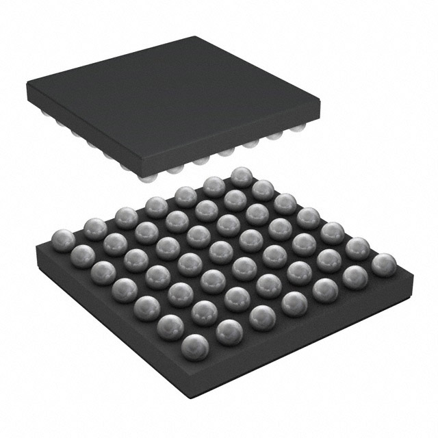


 工商网监
湘ICP备2023018690号
工商网监
湘ICP备2023018690号
