1N5518BUR-1 thru 1N5546BUR-1
Available on
commercial
versions
Qualified Levels:
JAN, JANTX and
JANTXV
Low Voltage Avalanche
500 mW Zener Diodes
Qualified per MIL-PRF-19500/437
DESCRIPTION
The 1N5518BUR-1 thru 1N5546BUR-1 series of 0.5 watt glass surface mount Zener voltage
regulators provides a selection from 3.3 to 33 volts with tolerances ranging from plus/minus
1% to 20%. The standard tolerance is plus/minus 5% with the B suffix unless ordered
otherwise. These glass surface mount devices are available with an internal metallurgical
bond option. This type of bonded Zener package construction is also in JAN, JANTX, and
JANTXV military qualifications. Microsemi also offers numerous other Zener products to meet
higher and lower power applications.
DO-213AA MELF
Package
Important: For the latest information, visit our website http://www.microsemi.com.
FEATURES
•
•
•
•
•
JEDEC registered 1N5518 thru 1N5546.
Voltage tolerances of plus/minus 20%, 10%, 5%, 2%, and 1% available. See Note 1 on page 3.
Internal metallurgical bond.
JAN, JANTX, and JANTXV qualification per MIL-PRF-19500/437 available.
RoHS compliant versions available (commercial grade only).
Also available in:
DO-35 (DO-204AH)
(axial-leaded)
1N5518B-1 thru 1N5546B-1
APPLICATIONS / BENEFITS
•
•
•
•
•
•
Regulates voltage over a broad operating current and temperature range.
Extensive selection from 3.3 to 33 V.
Hermetically sealed surface mount package.
Nonsensitive to ESD per MIL-STD-750 Method 1020.
Minimal capacitance (see Figure 3).
Inherently radiation hard as described in Microsemi’s “MicroNote 050” which is available at
Microsemi.com.
MAXIMUM RATINGS
Parameters/Test Conditions
Junction and Storage Temperature
(Note 1)
Steady-State Power
Symbol
Value
T J and T STG
PD
-65 to +175
0.5
R ӨJEC
R ӨJA
Z ӨJX
VF
T SP
100
300
35
1.1
260
Unit
o
C
W
(Also see derating in Figure 2)
(Note 2)
Thermal Resistance Junction-to-End Cap
(Note 2)
Thermal Resistance Junction-to-Ambient
Thermal Impedance
Forward Voltage
200mA
Solder Pad Temperature @ 10 s
o
C/W
C/W
o
C/W
V
o
C
o
Notes: 1. At end cap temperature T EC < 125 oC or at ambient T A < 50 ºC when mounted on FR4 PC board as
described for thermal resistance above (see Figure 2 for derating). Derate to 0 at +175 oC.
2. When mounted on FR4 PC board (1 oz Cu) with recommended footprint (see last page).
MSC – Lawrence
6 Lake Street,
Lawrence, MA 01841
1-800-446-1158
(978) 620-2600
Fax: (978) 689-0803
MSC – Ireland
Gort Road Business Park,
Ennis, Co. Clare, Ireland
Tel: +353 (0) 65 6840044
Fax: +353 (0) 65 6822298
Website:
www.microsemi.com
T4-LDS-0037, Rev 2 (111456)
©2011 Microsemi Corporation
Page 1 of 6
�1N5518BUR-1 thru 1N5546BUR-1
MECHANICAL and PACKAGING
•
•
•
•
•
•
•
•
CASE: Hermetically sealed glass DO-213AA (SOD80 or MLL34) MELF style package.
TERMINALS: End caps tin-lead plated or RoHS compliant matte-Tin plating available (on commercial only) solderable per MILSTD-750, method 2026.
POLARITY: Cathode indicated by band where diode is to be operated with the banded end positive with respect to the opposite
end for Zener regulation.
o
MOUNTING SURFACE SELECTION: The Axial Coefficient of Expansion (COE) of this device is approximately +6 PPM/ C. The
COE of the Mounting Surface System should be selected to provide a suitable match with this device.
MARKING: cathode band only.
TAPE & REEL option: Standard per EIA-481-1-A with 12 mm tape (add “TR” suffix to part number). Consult factory for quantities.
WEIGHT: 0.04 grams.
See Package Dimensions on last page.
PART NOMENCLATURE
JAN
1N5518 B UR -1 (e3)
Reliability Level
JAN = JAN Level
JANTX = JANTX Level
JANTXV = JANTXV Level
Blank = Commercial
RoHS Compliance
e3 = RoHS compliant (available
on commercial grady only)
Blank = non-RoHS compliant
Metallurgical Bond
-1 = Metallurgical bond
JEDEC type number
See Electrical Characteristics
table
Package type
UR = surface mount
Zener Voltage Tolerance
A = 10%
B = 5%
C = 2%
D = 1%
Blank = 20%
SYMBOLS & DEFINITIONS
Symbol
IR
I Z , I ZT , I ZK
I ZL
I ZM
VZ
∆V Z
Z ZT or Z ZK
Definition
Reverse Current: The maximum reverse (leakage) current that will flow at the specified voltage and temperature.
Regulator Current: The dc regulator current (I Z ), at a specified test point (I ZT ), near breakdown knee (I ZK ).
Low Regulator (Zener) Current: The lowest rated dc current for the specified power rating.
Maximum Regulator (Zener) Current: The maximum rated dc current for the specified power rating.
Zener Voltage: The zener voltage the device will exhibit at a specified current (I Z ) in its breakdown region.
Voltage Regulation: The change in zener voltage between two specified currents or percentage of I ZM .
Dynamic Impedance: The small signal impedance of the diode when biased to operate in its breakdown region at a
specified rms current modulation (typically 10% of I ZT or I ZK ) and superimposed on I ZT or I ZK respectively.
T4-LDS-0037, Rev 2 (111456)
©2011 Microsemi Corporation
Page 2 of 6
�1N5518BUR-1 thru 1N5546BUR-1
ELECTRICAL CHARACTERISTICS
(T A = 25oC unless otherwise noted. Based on DC measurements at thermal equilibrium; V F = 1.1 Max @ IF = 200 mA for all types.)
JEDEC TYPE
NUMBER
(Note 1)
1N5518BUR-1
1N5519BUR-1
1N5520BUR-1
1N5521BUR-1
1N5522BUR-1
1N5523BUR-1
1N5524BUR-1
1N5525BUR-1
1N5526BUR-1
1N5527BUR-1
1N5528BUR-1
1N5529BUR-1
1N5530BUR-1
1N5531BUR-1
1N5532BUR-1
1N5533BUR-1
1N5534BUR-1
1N5535BUR-1
1N5536BUR-1
1N5537BUR-1
1N5538BUR-1
1N5539BUR-1
1N5540BUR-1
1N5541BUR-1
1N5542BUR-1
1N5543BUR-1
1N5544BUR-1
1N5545BUR-1
1N5546BUR-1
NOMINAL
ZENER
VOLTAGE
TEST
CURRENT
I ZT
MAX. ZENER
IMPEDANCE
B-C-D SUFFIX
V Z @ I ZT
Z ZT @ I ZT
(Note 2)
(Note 3)
MAX. REVERSE CURRENT
(Note 4)
IR
V R – VOLTS
Volts
mA
Ohms
µA
NON &
ASUFFIX
3.3
3.6
3.9
4.3
4.7
5.1
5.6
6.2
6.8
7.5
8.2
9.1
10.0
11.0
12.0
13.0
14.0
15.0
16.0
17.0
18.0
19.0
20.0
22.0
24.0
25.0
28.0
30.0
33.0
20
20
20
20
10
5.0
3.0
1.0
1.0
1.0
1.0
1.0
1.0
1.0
1.0
1.0
1.0
1.0
1.0
1.0
1.0
1.0
1.0
1.0
1.0
1.0
1.0
1.0
1.0
26
24
22
18
22
26
30
30
30
35
40
45
60
80
90
90
100
100
100
100
100
100
100
100
100
100
100
100
100
5.0
3.0
1.0
3.0
2.0
2.0
2.0
1.0
1.0
0.5
0.5
0.1
0.05
0.05
0.05
0.01
0.01
0.01
0.01
0.01
0.01
0.01
0.01
0.01
0.01
0.01
0.01
0.01
0.01
0.90
0.90
0.90
1.0
1.5
2.0
3.0
4.5
5.5
6.0
6.5
7.0
8.0
9.0
9.5
10.5
11.5
12.5
13.0
14.0
15.0
16.0
17.0
18.0
20.0
21.0
23.0
24.0
28.0
B-C-D
SUFFIX
MAXIMUM
DC ZENER
CURRENT
B-C-D SUFFIX
MAX. NOISE
DENSITY
AT I Z = 250 µA
REGULATION
FACTOR
LOW V Z
CURRENT
∆V Z
I ZL
(Note 6)
(Note 6)
ND
I ZM
B-C-D
SUFFIX
(Note 5)
mA
µV/ √Hz
Volts
mA
1.0
1.0
1.0
1.5
2.0
2.5
3.5
5.0
6.2
6.8
7.5
8.2
9.1
9.9
10.8
11.7
12.6
13.5
14.4
15.3
16.2
17.1
18.0
19.8
21.6
22.4
25.2
27.0
29.7
115
105
98
88
81
75
68
61
56
51
46
42
38
35
32
29
27
25
24
22
21
20
19
17
16
15
14
13
12
0.5
0.5
0.5
0.5
0.5
0.5
1.0
1.0
1.0
2.0
4.0
4.0
4.0
5.0
10
15
20
20
20
20
20
20
20
25
30
35
40
45
50
0.90
0.90
0.85
0.75
0.60
0.65
0.30
0.20
0.10
0.05
0.05
0.05
0.10
0.20
0.20
0.20
0.20
0.20
0.20
0.20
0.20
0.20
0.20
0.25
0.30
0.35
0.40
0.45
0.50
2.0
2.0
2.0
2.0
1.0
0.25
0.25
0.01
0.01
0.01
0.01
0.01
0.01
0.01
0.01
0.01
0.01
0.01
0.01
0.01
0.01
0.01
0.01
0.01
0.01
0.01
0.01
0.01
0.01
NOTES:
1. TOLERANCE AND VOLTAGE DESIGNATION –
The JEDEC type numbers without a letter prior to the UR-1 suffix are +/-20% with guaranteed limits for only V Z , I R , and V F . Units with “A”
prior to the UR-1 suffix are +/-10% with guaranteed limits for V Z , I R , and V F . Units with guaranteed limits for all six parameters are
indicated by a B suffix for +/-5.0% units, C suffix for +/-2.0% and D suffix for +/-1.0% prior to the UR-1 suffix.
2. ZENER VOLTAGE (V Z ) MEASUREMENT –
Nominal zener voltage is measured with the device junction in thermal equilibrium with ambient temperature of 25 oC.
3. ZENER IMPEDANCE (Z Z ) MEASUREMENT –
The zener impedance is derived from the 60 Hz ac voltage, which results when an ac current having an rms value equal to 10% of the dc
zener current (I ZT ) is superimposed on I ZT .
4. REVERSE CURRENT (I R ) –
Reverse currents are guaranteed and are measured at V R as shown on the table.
5. MAXIMUM REGULATOR CURRENT (I ZM ) –
The maximum current shown is as shown in MIL-PRF-19500/437.
6. MAXIMUM REGULATION FACTOR (∆V Z ) –
∆V Z is the maximum difference between V Z at I ZT and V Z at I ZL measured with the device junction in thermal equilibrium.
T4-LDS-0037, Rev 2 (111456)
©2011 Microsemi Corporation
Page 3 of 6
�1N5518BUR-1 thru 1N5546BUR-1
GRAPHS
Pd, Rated Maximum dc Operation (mW)
Noise density, (ND) is specified in microvolt-rms per
square-root-hertz. Actual measurement is performed
using a 1 kHz to 3 kHz frequency bandpass filter at a
constant Zener test current (IZT) at 25 oC ambient
temperature.
o
T EC , End Cap Temperature ( C)
FIGURE 1 – Noise Density Measurement Circuit
Typical Capacitance in Picofarads (pf)
FIGURE 2 – Power Derating Curve
At zero volts
At –2 volts (VR)
Zener Voltage V Z
FIGURE 3 – Capacitance vs. Zener Voltage (Typical)
T4-LDS-0037, Rev 2 (111456)
FIGURE 4
Zener Diode Characteristics and Symbol Identification
©2011 Microsemi Corporation
Page 4 of 6
�1N5518BUR-1 thru 1N5546BUR-1
ZENER IMPEDANCE ZZT (Ohms)
GRAPHS (continued)
28 Volt
11 Volt
6.8 Volt
OPERATING CURRENT I ZT (mA)
FIGURE 5
ZENER IMPEDANCE vs. OPERATION CURRENT (typical)
T4-LDS-0037, Rev 2 (111456)
©2011 Microsemi Corporation
Page 5 of 6
�1N5518BUR-1 thru 1N5546BUR-1
PACKAGE DIMENSIONS
Ltr
BD
BL
ECT
S
Dimensions
Inch
Millimeter
Min
Max
Min
Max
.063
.067
1.60
1.70
.130
.146
3.30
3.71
.016
.022
0.41
0.56
.001 min
0.03 min
NOTES:
1. Dimensions are in inch.
2. Millimeters are given for general information only.
3. In accordance with ASME Y14.5M, diameters are equivalent to Φx symbology.
PAD LAYOUT
A
B
C
T4-LDS-0037, Rev 2 (111456)
INCHES
.200
.055
.080
©2011 Microsemi Corporation
mm
5.08
1.40
2.03
Page 6 of 6
�
很抱歉,暂时无法提供与“CDLL5546/TR”相匹配的价格&库存,您可以联系我们找货
免费人工找货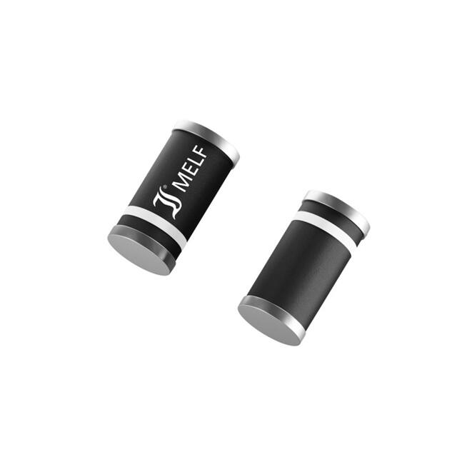


 工商网监
湘ICP备2023018690号
工商网监
湘ICP备2023018690号
