2N4261
Silicon PNP Transistor
D a ta S h e e t
Description
Applications
Semicoa offers:
• General purpose switching transistor
• Low power
• PNP silicon transistor
• Screening and processing per MIL-PRF-19500 Appendix E
• JAN level (2N4261J)
• JANTX level (2N4261JX)
• JANTXV level (2N4261JV)
• JANS level (2N4261JS)
• QCI to the applicable level
• 100% die visual inspection per MIL-STD-750 method
2072 for JANTXV and JANS
• Radiation testing (total dose) upon request
Features
•
•
•
•
Hermetically sealed TO-72 metal can
Also available in chip configuration
Chip geometry 0014
Reference document:
MIL-PRF-19500/511
Benefits
• Qualification Levels: JAN, JANTX,
JANTXV and JANS
• Radiation testing available
Please contact Semicoa for special configurations
www.SEMICOA.com or (714) 979-1900
Absolute Maximum Ratings
Parameter
Collector-Emitter Voltage
TC = 25°C unless otherwise specified
Symbol
VCEO
Rating
15
Collector-Base Voltage
VCBO
15
Unit
Volts
Volts
Emitter-Base Voltage
VEBO
4.5
Volts
Collector Current, Continuous
IC
30
mA
Power Dissipation, TA = 25°C
Derate linearly above 25°C
PT
200
1.14
Thermal Resistance
RθJA
0.86
mW
mW/°C
°C/mW
Operating Junction Temperature
Storage Temperature
TJ
TSTG
-65 to +200
°C
Copyright© 2005
Rev. E
SEMICOA
333 McCormick Avenue, Costa Mesa, California 92626 714.979.1900, FAX 714.557.4541
www.SEMICOA.com
Page 1 of 2
�2N4261
Silicon PNP Transistor
D a ta S h e e t
ELECTRICAL CHARACTERISTICS
characteristics specified at TA = 25°C
Off Characteristics
Parameter
Symbol
Collector-Emitter Breakdown Voltage
Collector-Base Cutoff Current
V(BR)CEO
Test Conditions
Min
IC = 10 mA
VCB = 15 Volts
10
µA
ICEX1
ICEX2
ICEX3
50
5
5
nA
nA
µA
5
nA
10
µA
IEBX
Emitter-Base Cutoff Current
IEBO
VEB = 4.5 Volts
Pulse Test: Pulse Width = 300 µs, Duty Cycle ≤ 2.0%
On Characteristics
Symbol
hFE1
hFE2
hFE3
hFE4
Test Conditions
IC = 1 mA, VCE = 1 Volts
IC = 10 mA, VCE = 1 Volts
IC = 30 mA, VCE = 1 Volts
IC = 10 mA, VCE = 1 Volts
TA = -55°C
VCE = 1 Volts, IC = 1 mA
VCE = 1 Volts, IC = 10 mA
IC = 1 mA, IB = 0.1 mA
IC = 10 mA, IB = 1 mA
Min
25
30
20
15
Min
rb’CC1
rb’CC2
Test Conditions
f = 100 MHz
VCE = 4 Volts, IC = 5 mA
VCE = 10 Volts, IC = 10 mA
VCB = 4 Volts, IE = 0 mA,
100 kHZ < f < 1 MHz
VEB = 0.5 Volts, IC = 0 mA,
100 kHZ < f < 1 MHz
VCE = 4 Volts, f = 31.8 MHz
IC = 5 mA
IC = 10 mA
Saturated Turn-On Time
tON
Saturated Turn-Off Time
tOFF
DC Current Gain
Base-Emitter Voltage
Collector-Emitter Saturation Voltage
Units
Volts
ICBO
Emitter-Base Cutoff Current
Parameter
Max
15
VCE = 10Volts, VBE = 0.4Volts
VCE = 10 Volts, VBE = 2 Volts
VCE = 10 Volts, VBE = 2 Volts,
TA = 150°C
VBE = 2 Volts, VCE = 10 Volts
Collector-Emitter Cutoff Current
Typ
VBE1
VBE2
VCEsat1
VCEsat2
Typ
Max
Units
150
0.8
1.0
0.15
0.35
Volts
Max
Units
2.5
pF
2.5
pF
60
50
ps
VCC = 17 Volts, IC = 10 mA
2.5
ns
VCC = 17 Volts, IC = 10 mA
3.5
ns
Volts
Dynamic Characteristics
Parameter
Symbol
Magnitude – Common Emitter, Short
Circuit Forward Current Transfer Ratio
|hFE1|
|hFE2|
Open Circuit Output Capacitance
COBO
Open Circuit Input Capacitance
CIBO
Collector Base time constant
Typ
15
20
Switching Characteristics
Copyright© 2005
Rev. E
SEMICOA
333 McCormick Avenue, Costa Mesa, California 92626 714.979.1900, FAX 714.557.4541
www.SEMICOA.com
Page 2 of 2
�
很抱歉,暂时无法提供与“JANTX2N4261”相匹配的价格&库存,您可以联系我们找货
免费人工找货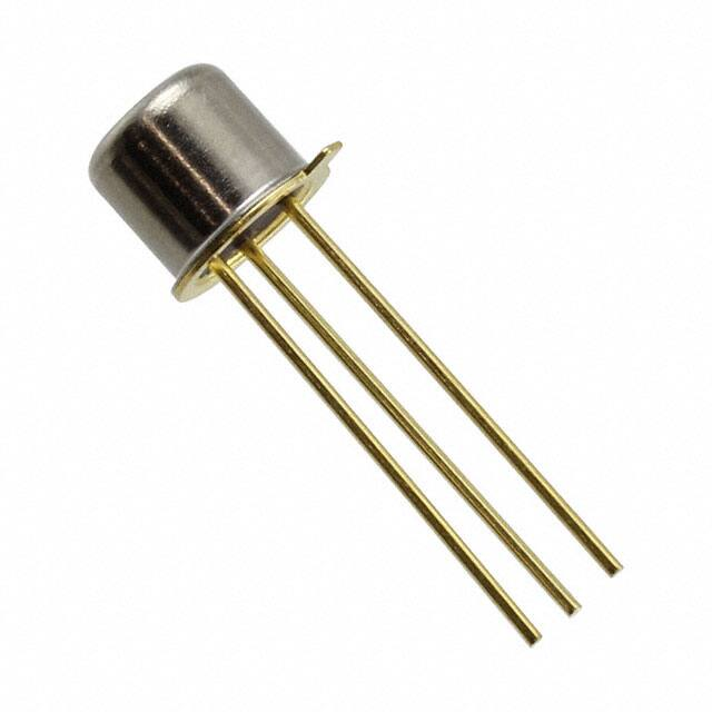


 工商网监
湘ICP备2023018690号
工商网监
湘ICP备2023018690号
