KSZ9131MNX
Gigabit Ethernet Transceiver with GMII/MII
Support
Features
Target Applications
• Single-Chip 10/100/1000 Mbps Ethernet Transceiver Suitable for IEEE 802.3 Applications
• GMII/MII Standard Interface with 3.3V/2.5V/1.8V
Tolerant I/Os
• Auto-Negotiation to Automatically Select the
Highest Link-Up Speed (10/100/1000 Mbps) and
Duplex (Half/Full)
• On-Chip Termination Resistors for the Differential
Pairs
• On-Chip LDO Controller to Support Single 3.3V
Supply Operation
• Jumbo Frame Support Up to 16 KB
• 125 MHz Reference Clock Output
• Energy-Detect Power-Down Mode for Reduced
Power Consumption When Cable is Not Attached
• Energy Efficient Ethernet (EEE) Support with
Low-Power Idle (LPI) Mode and Clock Stoppable
for 100BASE-TX/1000BASE-T and Transmit
Amplitude Reduction with 10BASE-Te Option
• Wake-On-LAN (WOL) Support with Robust
Custom-Packet Detection
• Programmable LED Outputs for Link, Activity, and
Speed
• Baseline Wander Correction
• Quiet-WIRE® EMI Reduction (100BASE-TX)
• LinkMD® TDR-based Cable Diagnostic to Identify
Faulty Copper Cabling
• Signal Quality Indication
• Parametric NAND Tree Support to Detect Faults
Between Chip I/Os and Board
• Loopback Modes for Diagnostics
• Automatic MDI/MDI-X Crossover to Detect and
Correct Pair Swap at All Speeds of Operation
• Automatic Detection and Correction of Pair
Swaps, Pair Skew, and Pair Polarity
• MDC/MDIO Management Interface for PHY Register Configuration
• Interrupt Pin Option
• Power-Down and Power-Saving Modes
• Operating Voltages
- Core (DVDDL, AVDDL, AVDDL_PLL): 1.2V
(External FET or Regulator)
- VDD I/O (DVDDH): 3.3V, 2.5V, or 1.8V
- Transceiver (AVDDH): 3.3V or 2.5V
• 64-pin QFN (8 mm × 8 mm) Package
•
•
•
•
•
•
•
•
•
•
•
2018-2019 Microchip Technology Inc.
Laser/Network Printer
Network Attached Storage (NAS)
Network Server
Broadband Gateway
Gigabit SOHO/SMB Router
IPTV
IP Set-Top Box
Game Console
IP Camera
Triple-Play (Data, Voice, Video) Media Center
Media Converter
DS00002840B-page 1
�KSZ9131MNX
TO OUR VALUED CUSTOMERS
It is our intention to provide our valued customers with the best documentation possible to ensure successful use of your Microchip
products. To this end, we will continue to improve our publications to better suit your needs. Our publications will be refined and
enhanced as new volumes and updates are introduced.
If you have any questions or comments regarding this publication, please contact the Marketing Communications Department via
E-mail at docerrors@microchip.com. We welcome your feedback.
Most Current Data Sheet
To obtain the most up-to-date version of this data sheet, please register at our Worldwide Web site at:
http://www.microchip.com
You can determine the version of a data sheet by examining its literature number found on the bottom outside corner of any page.
The last character of the literature number is the version number, (e.g., DS30000000A is version A of document DS30000000).
Errata
An errata sheet, describing minor operational differences from the data sheet and recommended workarounds, may exist for current devices. As device/documentation issues become known to us, we will publish an errata sheet. The errata will specify the
revision of silicon and revision of document to which it applies.
To determine if an errata sheet exists for a particular device, please check with one of the following:
• Microchip’s Worldwide Web site; http://www.microchip.com
• Your local Microchip sales office (see last page)
When contacting a sales office, please specify which device, revision of silicon and data sheet (include -literature number) you are
using.
Customer Notification System
Register on our web site at www.microchip.com to receive the most current information on all of our products.
DS00002840B-page 2
2018-2019 Microchip Technology Inc.
�KSZ9131MNX
Table of Contents
1.0 Preface ............................................................................................................................................................................................ 4
2.0 Introduction ..................................................................................................................................................................................... 8
3.0 Pin Descriptions and Configuration ................................................................................................................................................. 9
4.0 Functional Description .................................................................................................................................................................. 19
5.0 Register Descriptions .................................................................................................................................................................... 47
6.0 Operational Characteristics ......................................................................................................................................................... 116
7.0 Package Outline .......................................................................................................................................................................... 138
Appendix A: Data Sheet Revision History ......................................................................................................................................... 139
The Microchip Web Site .................................................................................................................................................................... 140
Customer Change Notification Service ............................................................................................................................................. 140
Customer Support ............................................................................................................................................................................. 140
Product Identification System ........................................................................................................................................................... 141
2018-2019 Microchip Technology Inc.
DS00002840B-page 3
�KSZ9131MNX
1.0
PREFACE
1.1
General Terms
TABLE 1-1:
GENERAL TERMS
Term
Description
1000BASE-T
1 Gbps Ethernet over twisted pair, IEEE 802.3 compliant
100BASE-TX
100 Mbps Ethernet over twisted pair, IEEE 802.3 compliant
10BASE-T
10 Mbps Ethernet over twisted pair, IEEE 802.3 compliant
ADC
Analog-to-Digital Converter
AFE
Analog Front End
AN, ANEG
Auto-Negotiation
AOAC
Always on Always Connected
ARP
Address Resolution Protocol
BELT
Best Effort Latency Tolerance
BYTE
8-bits
CSMA/CD
Carrier Sense Multiple Access/Collision Detect
CSR
Control and Status Register
DA
Destination Address
DCQ
Dynamic Channel Quality
DWORD
32-bits
EC
Embedded Controller
EEE
Energy Efficient Ethernet
FCS
Frame Check Sequence
FIFO
First In First Out buffer
FSM
Finite State Machine
FW
Firmware
GMII
Gigabit Media Independent Interface
GPIO
General Purpose I/O
HOST
External system (Includes processor, application software, etc.)
HW
Hardware. Refers to function implemented by digital logic.
IGMP
Internet Group Management Protocol
LDO
Linear Drop-Out Regulator
Level-Triggered Sticky Bit
This type of status bit is set whenever the condition that it represents is asserted.
The bit remains set until the condition is no longer true, and the status bit is cleared
by writing a zero.
LFSR
Linear Feedback Shift Register
LPM
Link Power Management
lsb
Least Significant Bit
DS00002840B-page 4
2018-2019 Microchip Technology Inc.
�KSZ9131MNX
TABLE 1-1:
GENERAL TERMS (CONTINUED)
Term
Description
LSB
Least Significant Byte
LTM
Latency Tolerance Messaging
MAC
Media Access Controller
MDI
Medium Dependent Interface
MDIX
Media Independent Interface with Crossover
MEF
Multiple Ethernet Frames
MII
Media Independent Interface
MLT-3
Multi-Level Transmission Encoding (3-Levels). A tri-level encoding method where a
change in the logic level represents a code bit “1” and the logic output remaining at
the same level represents a code bit “0”.
MSI / MSI-X
Message Signaled Interrupt
N/A
Not Applicable
OTP
One Time Programmable
PCS
Physical Coding Sublayer
PLL
Phase Locked Loop
PMIC
Power Management IC
POR
Power on Reset.
PTP
Precision Time Protocol
QWORD
64-bits
RESERVED
Refers to a reserved bit field or address. Unless otherwise noted, reserved bits must
always be zero for write operations. Unless otherwise noted, values are not guaranteed when reading reserved bits. Unless otherwise noted, do not read or write to
reserved addresses.
RMON
Remote Monitoring
SA
Source Address
SCSR
System Control and Status Registers
SEF
Single Ethernet Frame
SFD
Start of Frame Delimiter - The 8-bit value indicating the end of the preamble of an
Ethernet frame
SMNP
Simple Network Management Protocol
SQI
Signal Quality Indicator
UDP
User Datagram Protocol - A connectionless protocol run on top of IP networks
WORD
16-bits
2018-2019 Microchip Technology Inc.
DS00002840B-page 5
�KSZ9131MNX
1.2
Buffer Types
TABLE 1-2:
BUFFER TYPE DESCRIPTIONS
BUFFER
DESCRIPTION
AI
AI Analog input
AO
AI Analog output
AIO
AIO Analog bidirectional
ICLK
ICLK Crystal oscillator input pin
OCLK
OCLK Crystal oscillator output pin
VI
Variable voltage input
VIS
Variable voltage Schmitt-triggered input
VO8
Variable voltage output with 8 mA sink and 8 mA source
VOD8
Variable voltage open-drain output with 8 mA sink
VO24
Variable voltage output with 24 mA sink and 24 mA source
PU
44/59/96 KΩ (typical @3.3/2.5/1.8V) internal pull-up. Unless otherwise noted in the pin
description, internal pull-ups are always enabled.
Note:
PD
47/58/86 KΩ (typical @3.3/2.5/1.8V) internal pull-down. Unless otherwise noted in the pin
description, internal pull-downs are always enabled.
Note:
P
Internal pull-up resistors prevent unconnected inputs from floating. Do not rely on
internal resistors to drive signals external to the device. When connected to a load
that must be pulled high, an external resistor must be added.
Internal pull-down resistors prevent unconnected inputs from floating. Do not rely on
internal resistors to drive signals external to the device. When connected to a load
that must be pulled low, an external resistor must be added.
Power pin
Note:
Digital signals are not 5V tolerant unless specified.
Note:
Sink and source capabilities are dependent on the supplied voltage.
DS00002840B-page 6
2018-2019 Microchip Technology Inc.
�KSZ9131MNX
1.3
Register Bit Types
Table 1-3 describes the register but attributes used throughout this document.
TABLE 1-3:
REGISTER BIT TYPES
Register Bit Type Notation
Register Bit Description
R
W
RO
WO
W1S
W1C
WAC
RC
LL
LH
SC
Read: A register or bit with this attribute can be read.
Write: A register or bit with this attribute can be written.
Read only: Read only. Writes have no effect.
Write only: If a register or bit is write-only, reads will return unspecified data.
Write One to Set: Writing a one sets the value. Writing a zero has no effect.
Write One to Clear: Writing a one clears the value. Writing a zero has no effect.
Write Anything to Clear: Writing anything clears the value.
Read to Clear: Contents is cleared after the read. Writes have no effect.
Latch Low: Clear on read of register.
Latch High: Clear on read of register.
Self-Clearing: Contents is self-cleared after being set. Writes of zero have no effect.
Contents can be read.
Self-Setting: Contents is self-setting after being cleared. Writes of one have no effect.
Contents can be read.
Read Only, Latch High: This mode is used by the Ethernet PHY registers. Bits with this
attribute will stay high until the bit is read. After it a read, the bit will remain high, but will
change to low if the condition that caused the bit to go high is removed. If the bit has not
been read the bit will remain high regardless of if its cause has been removed.
Not Affected by Software Reset. The state of NASR bits does not change on assertion of a software reset.
This field is “Sticky” in that it is neither initialized nor modified by hot reset or Function
Level Reset.
Reserved Field: Reserved fields must be written with zeros, unless otherwise indicated, to ensure future compatibility. The value of reserved bits is not guaranteed on a
read.
SS
RO/LH
NASR
STKY
RESERVED
Many of these register bit notations can be combined. Come examples of this are:
• R/W: Can be written. Will return current setting on a read.
• R/WAC: Will return current setting on a read. Writing anything clears the bit.
1.4
1.
2.
3.
Reference Documents
IEEE 802.3TM-2015 IEEE Standard for Ethernet,
http://standards.ieee.org/about/get/802/802.3.html
IEEE 802.3bwTM-2015 IEEE Standard for Ethernet Amendment 1,
https://standards.ieee.org/findstds/standard/802.3bw-2015.html
OPEN Alliance TC1 - Advanced diagnostics features for 100BASE-T1 automotive Ethernet PHYs Version 1.0
http://www.opensig.org/download/document/218/Advanced_PHY_features_for_automotive_Ethernet_V1.0.pdf
2018-2019 Microchip Technology Inc.
DS00002840B-page 7
�KSZ9131MNX
2.0
INTRODUCTION
2.1
General Description
The KSZ9131MNX is a completely integrated triple-speed (10BASE-T/100BASE-TX/1000BASE-T) Ethernet physicallayer transceiver for transmission and reception of data on standard CAT-5 as well as CAT-5e and CAT-6 unshielded
twisted pair (UTP) cables.
The KSZ9131MNX offers the industry-standard GMII/MII (Gigabit Media Independent Interface/Media Independent
Interface) for connection to GMII/MII MACs in Gigabit Ethernet processors and switches for data transfer at 1000 Mbps
or 10/100 Mbps.
The KSZ9131MNX reduces board cost and simplifies board layout by using on-chip termination resistors for the four
differential pairs and by integrating an LDO controller to drive a low-cost MOSFET to supply the 1.2V core.
The KSZ9131MNX offers diagnostic features to facilitate system bring-up and debugging in production testing and in
product deployment. Parametric NAND tree support enables fault detection between KSZ9131MNX I/Os and the board.
The LinkMD® TDR-based cable diagnostic identifies faulty copper cabling. Remote, external, and local loopback functions verify analog and digital data paths.
The KSZ9131MNX is available in a 64-pin, RoHS Compliant QFN package.
FIGURE 2-1:
SYSTEM BLOCK DIAGRAM
10/100/1000Mbps
GMII/MII
Ethernet MAC
MDC/MDIO
MANAGEMENT
KSZ9131MNX
INT_N /
PME_N
/ LEDs
SYSTEM POWER CIRCUIT /
INTERUPT CONTROLLER /
LEDs
DS00002840B-page 8
VIN 3.3V,
2.5V
MAGNETICS
GMII/MII
ON-CHIP TERMINATION
RESISTORS
CRYSTAL
RJ-45
CONNECTOR
MEDIA TYPES
10BASE-T
100BASE-TX
1000BASE-T
LDO
CONTROLLER
VOUT 1.2V
2018-2019 Microchip Technology Inc.
�KSZ9131MNX
3.0
PIN DESCRIPTIONS AND CONFIGURATION
3.1
Pin Assignments
AGNDH
ISET
NC
XI
XO
AVDDL_PLL
LDO_O
TX_CLK
RESET_N
CLK125_NDO/LED_MODE
DVDDL
INT_N/PME_N2/ALLPHYAD
COL
MDIO
MDC
CRS
63
62
61
60
59
58
57
56
55
54
53
52
51
50
49
PIN ASSIGNMENTS (TOP VIEW)
64
FIGURE 3-1:
AVDDH
1
48
RX_CLK/PHYAD2
TXRXP_A
2
47
RX_ER
TXRXM_A
3
46
DVDDH
AVDDL
4
45
RX_DV/CLK125_EN
AVDDL
5
44
RXD0/MODE0
NC
6
43
RXD1/MODE1
TXRXP_B
7
42
DVDDL
TXRXM_B
8
41
RXD2/MODE2
40
DVDDH
KSZ9131MNX
64-Q FN
AGNDH
9
TXRXP_C
10
39
RXD3/MODE3
TXRXM_C
11
38
RXD4
AVDDL
12
37
RXD5
AVDDL
13
36
DVDDL
TXRXP_D
14
35
RXD6
34
RXD7
33
TX_EN
( T o p V i ew )
TXRXM_D
15
AVDDH
16
P_VSS
19
20
21
22
23
24
25
26
27
28
29
30
31
32
DVDDL
TXD0
TXD1
TXD2
TXD3
DVDDL
TXD4
TXD5
TXD6
TXD7
DVDDH
TX_ER
GTX_CLK
18
DVDDH
LED1/PME_N1//PHYAD0
17
LED2/PHYAD1
(Connect exposed pad to ground with a via field)
Note: Exposed pad (P_VSS) on bottom of package must be connected to ground with a via field.
Note: Configuration strap inputs are indicated with an underline.
2018-2019 Microchip Technology Inc.
DS00002840B-page 9
�KSZ9131MNX
TABLE 3-1:
KSZ9131MNX PIN ASSIGNMENTS
Pin
Num
Pin Name
Pin
Num
Pin Name
1
AVDDH
33
TX_EN
2
TXRXP_A
34
RXD7
3
TXRXM_A
35
RXD6
4
AVDDL
36
DVDDL
5
AVDDL
37
RXD5
6
NC
38
RXD4
7
TXRXP_B
39
RXD3/MODE3
8
TXRXM_B
40
DVDDH
9
AGNDH
41
RXD2/MODE2
10
TXRXP_C
42
DVDDL
11
TXRXM_C
43
RXD1/MODE1
12
AVDDL
44
RXD0/MODE0
13
AVDDL
45
RX_DV/CLK125_EN
14
TXRXP_D
46
DVDDH
15
TXRXM_D
47
RX_ER
16
AVDDH
48
RX_CLK/PHYAD2
17
LED2/PHYAD1
49
CRS
18
DVDDH
50
MDC
19
LED1/PME_N1/PHYAD0
51
MDIO
20
DVDDL
52
COL
21
TXD0
53
INT_N/PME_N2/ALLPHYAD
22
TXD1
54
DVDDL
23
TXD2
55
CLK125_NDO/LED_MODE
24
TXD3
56
RESET_N
25
DVDDL
57
TX_CLK
26
TXD4
58
LDO_O
27
TXD5
59
AVDDL_PLL
28
TXD6
60
XO
29
TXD7
61
XI
30
DVDDH
62
NC
31
TX_ER
63
ISET
32
GTX_CLK
64
AGNDH
Exposed Pad (P_VSS) must be connected to ground.
DS00002840B-page 10
2018-2019 Microchip Technology Inc.
�KSZ9131MNX
3.2
Pin Descriptions
This section contains descriptions of the various KSZ9131MNX pins. The “_N” symbol in the signal name indicates that
the active, or asserted, state occurs when the signal is at a low voltage level. For example, RESET_N indicates that the
reset signal is active low. When “_N” is not present after the signal name, the signal is asserted when at the high voltage
level.
The pin function descriptions have been broken into functional groups as follows:
•
•
•
•
•
•
Analog Front End
GMII Interface
Crystal
Miscellaneous
Strap Inputs
I/O Power, Core Power and Ground
TABLE 3-2:
ANALOG FRONT END
Name
Symbol
BUFFER
TYPE
Ethernet TX/RX
Positive Channel
A
TXRXP_A
AIO
Ethernet TX/RX
Negative Channel
A
Ethernet TX/RX
Positive Channel
B
Ethernet TX/RX
Negative Channel
B
Ethernet TX/RX
Positive Channel
C
DESCRIPTION
Media Dependent Interface[0], positive signal of differential
pair
1000BT mode: TXRXP_A corresponds to BI_DA+.
TXRXM_A
AIO
10BT/100BT mode: TXRXP_A is the positive transmit signal
(TX+) for MDI configuration and the positive receive signal
(RX+) for MDI-X configuration, respectively.
Media Dependent Interface[0], negative signal of differential
pair
1000BT mode: TXRXM_A corresponds to BI_DA-.
TXRXP_B
AIO
10BT/100BT-TX mode: TXRXM_A is the negative transmit signal (TX-) for MDI configuration and the negative receive signal
(RX-) for MDI-X configuration, respectively.
Media Dependent Interface[1], positive signal of differential
pair
1000BT mode: TXRXP_B corresponds to BI_DB+.
TXRXM_B
AIO
10BT/100BT mode: TXRXP_B is the positive receive signal
(RX+) for MDI configuration and the positive transmit signal
(TX+) for MDI-X configuration, respectively.
Media Dependent Interface[1], negative signal of differential
pair
1000BT mode: TXRXM_B corresponds to BI_DB-.
TXRXP_C
AIO
10BT/100BT mode: TXRXP_B is the negative receive signal
(RX-) for MDI configuration and the negative transmit signal
(TX-) for MDI-X configuration, respectively.
Media Dependent Interface[2], positive signal of differential
pair
1000BT mode: TXRXP_C corresponds to BI_DC+.
10BT/100BT mode: TXRXP_C is not used.
2018-2019 Microchip Technology Inc.
DS00002840B-page 11
�KSZ9131MNX
TABLE 3-2:
ANALOG FRONT END (CONTINUED)
Name
Symbol
BUFFER
TYPE
Ethernet TX/RX
Negative Channel
C
TXRXM_C
AIO
Ethernet TX/RX
Positive Channel
D
TXRXP_D
Ethernet TX/RX
Negative Channel
D
TXRXM_D
DESCRIPTION
Media Dependent Interface[2], negative signal of differential
pair
1000BT mode: TXRXM_C corresponds to BI_DC-.
AIO
10BT/100BT mode: TXRXM_C is not used.
Media Dependent Interface[3], positive signal of differential
pair
1000BT mode: TXRXP_D corresponds to BI_DD+.
AIO
10BT/100BT mode: TXRXP_D is not used.
Media Dependent Interface[3], negative signal of differential
pair
1000BT mode: TXRXM_D corresponds to BI_DD-.
10BT/100BT mode: TXRXM_D is not used.
TABLE 3-3:
GMII INTERFACE
Name
Symbol
Transmit Data
TXD7
TXD6
TXD5
TXD4
TXD3
TXD2
TXD1
TXD0
TX_EN
TX_ER
Transmit Enable
Transmit Error
BUFFER
TYPE
DESCRIPTION
VI
(PD)
The MAC transmits data to the PHY using these signals.
VI
VI
(PD)
Indicates the presence of valid data on TXD[7:0].
Indicates a transmit error condition during frame transmission.
Note:
Bits 7-4 are not used in MII mode and if not driven,
require external pull-down resistors.
Also used to request Low Power Idle for Energy Efficient
Ethernet operation.
Note:
VI
If the GMII/MII MAC does not provide the TX_ER
output signal, this pin should be tied low.
GMII transmit reference clock.
GMII Transmit
Clock
GTX_CLK
MII Transmit Clock
TX_CLK
VO24
This signal is not used in MII mode and if not driven,
requires an external pull-down resistor.
MII transmit reference clock.
Collision Detect
COL
VO24
Note:
This signal is not used in GMII mode.
Asserted to indicate detection of a collision condition.
Carrier Sense
CRS
VO24
Note:
Used in half-duplex mode only.
Indicates detection of carrier.
Note:
Note:
DS00002840B-page 12
Used in half-duplex mode only.
2018-2019 Microchip Technology Inc.
�KSZ9131MNX
TABLE 3-3:
GMII INTERFACE (CONTINUED)
BUFFER
TYPE
Name
Symbol
Receive Data
VO24
Receive Data Valid
RXD7
RXD6
RXD5
RXD4
RXD3
RXD2
RXD1
RXD0
RX_DV
Receive Error
RX_ER
VO24
Receive Clock
TABLE 3-4:
RX_CLK
DESCRIPTION
The PHY transfers data to the MAC using these signals.
Note:
VO24
VO24
Bits 7-4 are not used in MII mode and are driven low.
Indicates that recovered and decoded data is being presented
on the receive data pins.
Asserted to indicate an error has been detected in the frame
presently being transferred from the PHY.
Also used to indicate Low Power Idle for Energy Efficient
Ethernet operation.
Receive reference clock.
CRYSTAL
Name
Symbol
BUFFER
TYPE
Crystal Input
XI
ICLK
DESCRIPTION
When using a 25MHz crystal, this input is connected to one
lead of the crystal.
When using an clock source, this is the input from the oscillator.
Note:
Crystal Output
XO
OCLK
The crystal or oscillator should have a tolerance of
±50ppm.
When using a 25MHz crystal, this output is connected to one
lead of the crystal.
When using an external oscillator, this pin is not connected.
2018-2019 Microchip Technology Inc.
DS00002840B-page 13
�KSZ9131MNX
TABLE 3-5:
MISCELLANEOUS
Name
Symbol
Indicator LEDs
LED2
LED1
MDIO
Management
Interface Data
Management
Interface Clock
Power Management Event
PME_N2
PME_N1
PHY Interrupt
CLK125 MHz
INT_N
CLK125_NDO
System Reset
LDO Controller
Output
MDC
RESET_N
LDO_O
BUFFER
TYPE
VO8
VIS/
VO8
VOD8
(PU)
VIS
(PU)
VO8
DESCRIPTION
Programmable LED outputs.
This is the management data from/to the MAC.
Note:
An external pull-up resistor to DVDDH in the range
of 1.0 kΩ to 4.7 kΩ is required.
This is the management clock input from the MAC.
Programmable PME_N output.
When asserted low, this pin signals that a WOL event has
occurred.
VO8
VO24
VIS
(PU)
AO
PME_N can be mapped to either (or both) pins.
Programmable interrupt output.
125 MHz clock output.
This pin provides a 125 MHz reference clock output option for
use by the MAC.
This pin may also provide a 125 MHz clock output synchronous to the receive data for use in Synchronous Ethernet
(SyncE) applications.
Chip reset (active low).
Hardware pin configurations are strapped-in at the de-assertion (rising edge) of RESET_N. See the Strap Inputs section
for details.
On-chip 1.2V LDO controller output.
This pin drives the input gate of a P-channel MOSFET to generate 1.2V for the chip’s core voltages.
Note:
PHY Bias Resistor
No Connect
ISET
NC
AI
-
If the system provides 1.2V, this pin is not used and
can be left unconnected.
This pin should be connect to ground through a 6.04KΩ 1%
resistor.
APPLICATION NOTE: The resistor value is different from
the 12.1KΩ used on the KSZ9031.
For normal operation, these pins should be left unconnected.
Note:
DS00002840B-page 14
Pin 62 is not bonded and can be connected to
AVDDH power for footprint compatibility with older
generation devices.
2018-2019 Microchip Technology Inc.
�KSZ9131MNX
TABLE 3-6:
STRAP INPUTS
BUFFER
TYPE
Name
Symbol
PHY Address
PHYAD2
PHYAD1
PHYAD0
VI
All PHY Address
Enable
ALLPHYAD
VI
DESCRIPTION
The PHY address, PHYAD[2:0], is sampled and latched at
power-up/reset and is configurable to any value from 0 to 7.
Each PHY address bit is configured as follows:
Pulled-up = 1
Pulled-down = 0
PHY Address Bits [4:3] are always set to ‘00’.
The ALLPHYAD strap-in pin is sampled and latched at powerup/reset and are defined as follows:
0 = PHY will respond to PHY address 0 as well as it’s assigned
PHY address
1= PHY will respond to only it’s assigned PHY address
Note:
Device Mode
125MHz Output
Clock Enable
LED Mode
MODE3
MODE2
MODE1
MODE0
CLK125_EN
LED_MODE
2018-2019 Microchip Technology Inc.
This strap input is inverted compared to the AllPHYAD Enable register bit.
The MODE[3:0] strap-in pins are sampled and
latched at power-up/reset and are defined in Section
3.3.1, "Device Mode Select"
VI
Note:
VI
CLK125_EN is sampled and latched at power-up/reset and is
defined as follows:
Pulled-up (1) = Enable 125 MHz clock output
Pulled-down (0) = Disable 125 MHz clock output
VI
CLK125_NDO provides the 125 MHz reference clock output
option for use by the MAC.
LED_MODE is sampled and latched at power-up/reset and is
defined as follows:
Pulled-up (1) = Individual-LED mode
Pulled-down (0) = Tri-color-LED mode
DS00002840B-page 15
�KSZ9131MNX
TABLE 3-7:
I/O POWER, CORE POWER AND GROUND
Name
Symbol
BUFFER
TYPE
+2.5/3.3V
Analog Power
Supply
AVDDH
P
+2.5/3.3V analog power supply VDD
+1.2V Analog
Power Supply
AVDDL
P
+1.2V analog power supply VDD
+1.2V Analog
PLL Power
Supply
AVDDL_PLL
P
+1.2V analog PLL power supply VDD
+3.3/2.5/1.8V
Variable I/O
Power Supply
Input
DVDDH
P
+3.3/2.5/1.8V variable I/O digital power supply VDD_IO
+1.2V Digital
Core Power
Supply Input
DVDDL
P
+1.2V digital core power supply input
Paddle Ground
P_VSS
GND
Common ground. This exposed paddle must be connected to
the ground plane with a via array.
Analog Ground
High
AGNDH
GND
Analog ground high
DS00002840B-page 16
DESCRIPTION
2018-2019 Microchip Technology Inc.
�KSZ9131MNX
3.3
Configuration Straps
Configuration straps allow various features of the device to be automatically configured to user defined values. Configuration straps are latched upon the release of pin reset (RESET_N). Configuration straps do not include internal resistors and require the use of external resistors.
Note:
• The system designer must ensure that configuration strap pins meet the timing requirements specified in Section
6.6.3, "Reset Pin Configuration Strap Timing". If configuration strap pins are not at the correct voltage level prior
to being latched, the device may capture incorrect strap values.
• When externally pulling configuration straps high, the strap should be tied to DVDDH.
APPLICATION NOTE: All straps should be pulled-up or pulled-down externally on the PCB to enable the desired
operational state.
3.3.1
DEVICE MODE SELECT
The MODE[3:0] configuration straps selects the device mode as follows:
TABLE 3-8:
DEVICE MODE SELECTIONS
Functional Modes
MODE[3:0]
Mode
0000
0001
1000
1001
RESERVED
GMII/MII
RESERVED
GMII/MII
1010
1011
RESERVED
GMII/MII
1100
1101
1110
1111
RESERVED
RESERVED
RESERVED
RESERVED
Auto-negotiation Advertisement
PME Pin
Enable
LED1
(PME_N1)
INT_N
(PME_N2)
1000BT Full
Duplex
1000BT Half
Duplex
10/100BT Full
Duplex
10/100BT Half
Duplex
yes
yes
no
no
yes
yes
yes
yes
yes
no
yes
yes
-
-
-
-
Test Modes
MODE[3:0]
0010
0011
0100
0101
0110
0111
Mode
RESERVED
RESERVED
NAND tree mode
RESERVED
RESERVED
Device power down mode
2018-2019 Microchip Technology Inc.
DS00002840B-page 17
�KSZ9131MNX
3.3.2
PHY ADDRESS
The PHYAD2:0 configuration straps set the value of the PHY’s management address. PHY Address Bits [4:3] are always
set to ‘00’.
3.3.3
ALL PHYs ADDRESS
The ALLPHYAD configuration strap sets the default of the All-PHYAD Enable bit in the Common Control Register which
enables or disables the PHY’s ability to respond to PHY address 0 as well as it’s assigned PHY address.
Note:
3.3.4
This strap input is inverted compared to the register bit.
125MHZ OUTPUT CLOCK ENABLE
The CLK125_EN configuration strap enables the 125 MHz clock output onto the CLK125_NDO pin.
The output clock defaults to a locally generated 125MHz clock. The recovered 125MHz RX clock can be selected for
use in Synchronous Ethernet (SyncE) applications.
3.3.5
LED MODE SELECT
The LED_MODE configuration strap selects between Individual-LED (1) or Tri-color-LED (0) modes. LED operation is
described in Section 4.13, "LED Support".
DS00002840B-page 18
2018-2019 Microchip Technology Inc.
�KSZ9131MNX
4.0
FUNCTIONAL DESCRIPTION
The KSZ9131MNX is a completely integrated triple-speed (10BASE-T/100BASE-TX/1000BASE-T) Ethernet physical
layer transceiver solution for transmission and reception of data over a standard CAT-5 unshielded twisted pair (UTP)
cable.
The KSZ9131MNX reduces board cost and simplifies board layout by using on-chip termination resistors for the four
differential pairs and by integrating an LDO controller to drive a low-cost MOSFET to supply the 1.2V core.
On the copper media interface, the KSZ9131MNX can automatically detect and correct for differential pair misplacements and polarity reversals, and correct propagation delays and re-sync timing between the four differential pairs, as
specified in the IEEE 802.3 standard for 1000BASE-T operation.
The KSZ9131MNX provides the GMII/MII interface for connection to GMACs in Gigabit Ethernet processors and
switches for data transfer at 10/100/1000Mbps.
Figure 4-1 shows a high-level block diagram of the KSZ9131MNX.
FIGURE 4-1:
KSZ9131MNX BLOCK DIAGRAM
PMA
TX10/100/1000
CLOCK
RESET
CONFIGURATIONS
PMA
RX1000
PCS1000
MEDIA
INTERFACE
PMA
RX100
PCS100
PMA
RX10
PCS10
AUTONEGOTIATION
4.1
4.1.1
GMII/MII
INTERFACE
LED
DRIVERS
10BASE-T/100BASE-TX Transceiver
100BASE-TX TRANSMIT
The 100BASE-TX transmit function performs parallel-to-serial conversion, 4B/5B coding, scrambling, NRZ-to-NRZI conversion, and MLT-3 encoding and transmission.
The circuitry starts with a parallel-to-serial conversion, which converts the MII data from the MAC into a 125 MHz serial
bit stream. The data and control stream is then converted into 4B/5B coding, followed by a scrambler. The serialized
data is further converted from NRZ-to-NRZI format, and then transmitted in MLT-3 current output. The output current is
set by an external 6.04 kΩ 1% resistor for the 1:1 transformer ratio.
The output signal has a typical rise/fall time of 4 ns and complies with the ANSI TP-PMD standard regarding amplitude
balance, and overshoot. The wave-shaped 10BASE-T output is also incorporated into the 100BASE-TX transmitter.
4.1.2
100BASE-TX RECEIVE
The 100BASE-TX receiver function performs adaptive equalization, DC restoration, MLT-3-to-NRZI conversion, data
and clock recovery, NRZI-to-NRZ conversion, de-scrambling, 4B/5B decoding, and serial-to-parallel conversion.
2018-2019 Microchip Technology Inc.
DS00002840B-page 19
�KSZ9131MNX
The receiving side starts with the equalization filter to compensate for inter-symbol interference (ISI) over the twisted
pair cable. Because the amplitude loss and phase distortion are a function of the cable length, the equalizer must adjust
its characteristics to optimize performance. In this design, the variable equalizer makes an initial estimation based on
comparisons of incoming signal strength against some known cable characteristics, then tunes itself for optimization.
This is an ongoing process and self-adjusts against environmental changes such as temperature variations.
Next, the equalized signal goes through a DC-restoration and data-conversion block. The DC-restoration circuit compensates for the effect of baseline wander and improves the dynamic range. The differential data conversion circuit converts the MLT-3 format back to NRZI. The slicing threshold is also adaptive.
The clock-recovery circuit extracts the 125 MHz clock from the edges of the NRZI signal. This recovered clock is then
used to convert the NRZI signal into the NRZ format. This signal is sent through the de-scrambler followed by the 4B/
5B decoder. Finally, the NRZ serial data is converted to the GMII/MII format and provided as the input data to the MAC.
4.1.3
SCRAMBLER/DE-SCRAMBLER (100BASE-TX ONLY)
The purpose of the scrambler is to spread the power spectrum of the signal to reduce electromagnetic interference (EMI)
and baseline wander. Transmitted data is scrambled using an 11-bit wide linear feedback shift register (LFSR). The
scrambler generates a 2047-bit non-repetitive sequence, then the receiver de-scrambles the incoming data stream
using the same sequence as at the transmitter.
4.1.4
10BASE-T TRANSMIT
The 10BASE-T output drivers are incorporated into the 100BASE-TX drivers to allow for transmission with the same
magnetic. The drivers perform internal wave-shaping and pre-emphasis, and output signals with typical amplitude of
2.5V peak for standard 10BASE-T mode and 1.75V peak for energy-efficient 10BASE-Te mode. The 10BASE-T/
10BASE-Te signals have harmonic contents that are at least 31 dB below the fundamental frequency when driven by
an all-ones Manchester-encoded signal.
4.1.5
10BASE-T RECEIVE
On the receive side, input buffer and level-detecting squelch circuits are used. A differential input receiver circuit and a
phase-locked loop (PLL) perform the decoding function. The Manchester-encoded data stream is separated into clock
signal and NRZ data. A squelch circuit rejects signals with levels less than 300 mV or with short pulse widths to prevent
noises at the receive inputs from falsely triggering the decoder. When the input exceeds the squelch limit, the PLL locks
onto the incoming signal and the KSZ9131MNX decodes a data frame. The receiver clock is maintained active during
idle periods between receiving data frames.
The KSZ9131MNX removes all 7 bytes of the preamble and presents the received frame starting with the SFD (start of
frame delimiter) to the MAC.
Auto-polarity correction is provided for the receiving differential pair to automatically swap and fix the incorrect +/– polarity wiring in the cabling.
4.2
1000BASE-T Transceiver
The 1000BASE-T transceiver is based-on a mixed-signal/digital-signal processing (DSP) architecture, which includes
the analog front-end, digital channel equalizers, trellis encoders/decoders, echo cancelers, cross-talk cancelers, precision clock recovery scheme, and power-efficient line drivers.
Figure 4-2 shows a high-level block diagram of a single channel of the 1000BASE-T transceiver for one of the four differential pairs.
DS00002840B-page 20
2018-2019 Microchip Technology Inc.
�KSZ9131MNX
FIGURE 4-2:
KSZ9131 1000BASE-T BLOCK DIAGRAM - SINGLE CHANNEL
XTAL
OTHER
CHANNELS
CLOCK
GENERATION
TX
SIGNAL
SIDE -STREAM
SCRAMBLER
&
SYMBOL ENCODER
TRANSMIT
BLOCK
PCS STATE
MACHINES
LED DRIVER
NEXT
CANCELLER
NEXT
Canceller
NEXT Canceller
ECHO
CANCELLER
ANALOG
HYBRID
PAIR SWAP
&
ALIGN UNIT
BASELINE
WANDER
COMPENSATION
RXADC
AGC
RX
SIGNAL
FFE
+
CLOCK & PHASE
RECOVERY
AUTO NEGOTIATION
DESCRAMBLER
+
DECODER
SLICER
DFE
MII
REGISTERS
MII
MANAGEMENT
CONTROL
PMA STATE
MACHINES
4.2.1
ANALOG ECHO-CANCELLATION CIRCUIT
In 1000BASE-T mode, the analog echo-cancellation circuit helps to reduce the near-end echo. This analog hybrid circuit
relieves the burden of the ADC and the adaptive equalizer.
This circuit is disabled in 10BASE-T/100BASE-TX mode.
4.2.2
AUTOMATIC GAIN CONTROL (AGC)
In 1000BASE-T mode, the automatic gain control (AGC) circuit provides initial gain adjustment to boost up the signal
level. This pre-conditioning circuit is used to improve the signal-to-noise ratio of the receive signal.
4.2.3
ANALOG-TO-DIGITAL CONVERTER (ADC)
In 1000BASE-T mode, the analog-to-digital converter (ADC) digitizes the incoming signal. ADC performance is essential to the overall performance of the transceiver.
This circuit is disabled in 10BASE-T/100BASE-TX mode.
4.2.4
TIMING RECOVERY CIRCUIT
In 1000BASE-T mode, the mixed-signal clock recovery circuit together with the digital phase-locked loop is used to
recover and track the incoming timing information from the received data. The digital phase-locked loop has very low
long-term jitter to maximize the signal-to-noise ratio of the receive signal.
The 1000BASE-T slave PHY must transmit the exact receive clock frequency recovered from the received data back to
the 1000BASE-T master PHY. Otherwise, the master and slave will not be synchronized after long transmission. This
also helps to facilitate echo cancellation and NEXT removal.
4.2.5
ADAPTIVE EQUALIZER
In 1000BASE-T mode, the adaptive equalizer provides the following functions:
• Detection for partial response signaling
• Removal of NEXT and ECHO noise
• Channel equalization
Signal quality is degraded by residual echo that is not removed by the analog hybrid because of impedance mismatch.
The KSZ9131MNX uses a digital echo canceler to further reduce echo components on the receive signal.
In 1000BASE-T mode, data transmission and reception occurs simultaneously on all four pairs of wires (four channels).
This results in high-frequency cross-talk coming from adjacent wires. The KSZ9131MNX uses three NEXT cancelers
on each receive channel to minimize the cross-talk induced by the other three channels.
2018-2019 Microchip Technology Inc.
DS00002840B-page 21
�KSZ9131MNX
In 10BASE-T/100BASE-TX mode, the adaptive equalizer needs only to remove the inter-symbol interference and
recover the channel loss from the incoming data.
4.2.6
TRELLIS ENCODER AND DECODER
In 1000BASE-T mode, the transmitted 8-bit data is scrambled into 9-bit symbols and further encoded into 4D-PAM5
symbols. The initial scrambler seed is determined by the specific PHY address to reduce EMI when more than one
KSZ9131 is used on the same board. On the receiving side, the idle stream is examined first. The scrambler seed, pair
skew, pair order, and polarity must be resolved through the logic. The incoming 4D-PAM5 data is then converted into 9bit symbols and de-scrambled into 8-bit data.
4.3
Auto MDI/MDI-X
The Automatic MDI/MDI-X feature eliminates the need to determine whether to use a straight cable or a crossover cable
between the KSZ9131MNX and its link partner. This auto-sense function detects the MDI/MDI-X pair mapping from the
link partner, and assigns the MDI/MDI-X pair mapping of the KSZ9131MNX accordingly.
Table 4-1 shows the KSZ9131MNX 10/100/1000 pin configuration assignments for MDI/MDI-X pin mapping.
TABLE 4-1:
Pin
(RJ-45 Pair)
MDI/MDI-X PIN MAPPING
MDI
MDI-X
1000BASE-T
100BASE-T
10BASE-T
1000BASE-T
100BASE-T
10BASE-T
TXRXP/M_A
(1, 2)
A+/–
TX+/–
TX+/–
A+/–
RX+/–
RX+/–
TXRXP/M_B
(3, 6)
B+/–
RX+/–
RX+/–
B+/–
TX+/–
TX+/–
TXRXP/M_C
(4, 5)
C+/–
Not Used
Not Used
C+/–
Not Used
Not Used
TXRXP/M_D
(7, 8)
D+/–
Not Used
Not Used
D+/–
Not Used
Not Used
Auto MDI/MDI-X is enabled by default. It is disabled by writing a one to the Swap-Off bit in the Auto-MDI/MDI-X Register.
MDI and MDI-X mode is set by the MDI Set bit in the Auto-MDI/MDI-X Register if Auto MDI/MDI-X is disabled.
An isolation transformer with symmetrical transmit and receive data paths is recommended to support Auto MDI/MDI-X.
4.4
Pair-Swap, Alignment, and Polarity Check
In 1000BASE-T mode, the KSZ9131MNX
• Detects incorrect channel order and automatically restores the pair order for the A, B, C, D pairs (four channels).
• Supports 50 ns ±10 ns difference in propagation delay between pairs of channels in accordance with the IEEE
802.3 standard, and automatically corrects the data skew so the corrected four pairs of data symbols are synchronized.
Incorrect pair polarities of the differential signals are automatically corrected for all speeds.
4.5
Wave Shaping, Slew-Rate Control, and Partial Response
In communication systems, signal transmission encoding methods are used to provide the noise-shaping feature and
to minimize distortion and error in the transmission channel.
• For 1000BASE-T, a special partial-response signaling method is used to provide the band-limiting feature for the
transmission path.
• For 100BASE-TX, a simple slew-rate control method is used to minimize EMI.
• For 10BASE-T, pre-emphasis is used to extend the signal quality through the cable.
4.6
PLL Clock Synthesizer
The KSZ9131MNX generates 125 MHz, 25 MHz, and 10 MHz clocks for system timing. Internal clocks are generated
from the external 25 MHz crystal or reference clock.
DS00002840B-page 22
2018-2019 Microchip Technology Inc.
�KSZ9131MNX
4.7
Auto-Negotiation
The KSZ9131MNX conforms to the auto-negotiation protocol, defined in Clause 28 of the IEEE 802.3 Specification.
Auto-negotiation allows UTP (unshielded twisted pair) link partners to select the highest common mode of operation.
During auto-negotiation, link partners advertise capabilities across the UTP link to each other, and then compare their
own capabilities with those they received from their link partners. The highest speed and duplex setting that is common
to the two link partners is selected as the operating mode.
The following list shows the speed and duplex operation mode from highest-to-lowest:
• Priority 1: 1000BASE-T, full-duplex
• Priority 2: 1000BASE-T, half-duplex
Note:
•
•
•
•
The device does not support 1000BASE-T, half-duplex and should not be enabled to advertise such.
Priority 3: 100BASE-TX, full-duplex
Priority 4: 100BASE-TX, half-duplex
Priority 5: 10BASE-T, full-duplex
Priority 6: 10BASE-T, half-duplex
If auto-negotiation is not supported or the KSZ9131MNX link partner is forced to bypass auto-negotiation for 10BASET and 100BASE-TX modes, the KSZ9131MNX sets its operating mode by observing the input signal at its receiver. This
is known as parallel detection, and allows the KSZ9131MNX to establish a link by listening for a fixed signal protocol in
the absence of the auto-negotiation advertisement protocol.
The auto-negotiation link-up process is shown in Figure 4-3.
FIGURE 4-3:
AUTO-NEGOTIATION FLOW CHART
START AUTO-NEGOTIATION
FORCE LINK SETTING
NO
PARALLEL
OPERATION
YES
BYPASS AUTO-NEGOTIATION
AND SET LINK MODE
ATTEMPT AUTONEGOTIATION
LISTEN FOR 100BASE-TX
IDLES
LISTEN FOR 10BASE-T
LINK PULSES
NO
JOIN FLOW
LINK MODE SET?
YES
LINK MODE SET
For 1000BASE-T mode, auto-negotiation is required and always used to establish a link. During 1000BASE-T autonegotiation, the master and slave configuration is first resolved between link partners. Then the link is established with
the highest common capabilities between link partners.
Auto-negotiation is enabled by default after power-up or hardware reset. After that, auto-negotiation can be enabled or
disabled through the Auto-Negotiation Enable bit in the Basic Control Register. If auto-negotiation is disabled, the speed
is set by the Speed Select[0] and Speed Select[1] bits and the duplex is set by the Duplex Mode, all in the Basic Control
Register.
If the speed is changed on the fly, the link goes down and either auto-negotiation or parallel detection initiates until a
common speed between KSZ9131MNX and its link partner is re-established for a link.
2018-2019 Microchip Technology Inc.
DS00002840B-page 23
�KSZ9131MNX
If the link is already established and there is no change of speed on the fly, the changes (for example, duplex and pause
capabilities) will not take effect unless either auto-negotiation is restarted through the Restart Auto-Negotiation
(PHY_RST_AN) bit in the Basic Control Register, or a link-down to link-up transition occurs (that is, disconnecting and
reconnecting the cable).
After auto-negotiation is completed, the link status is updated in the Link Status bit of the Basic Status Register and the
link partner capabilities are updated in the Auto-Negotiation Link Partner Base Page Ability Register, Auto-Negotiation
Expansion Register, and Auto-Negotiation Master Slave Status Register.
The auto-negotiation finite state machines use interval timers to manage the auto-negotiation process. The duration of
these timers under normal operating conditions is summarized in Table 4-2.
TABLE 4-2:
AUTO-NEGOTIATION TIMERS
Auto-Negotiation Interval Timers
Time Duration
Transmit Burst Interval
16 ms
Transmit Pulse Interval
68 µs
FLP Detect Minimum Time
17.2 µs
FLP Detect Maximum Time
185 µs
Receive Minimum Burst Interval
6.8 ms
Receive Maximum Burst Interval
112 ms
Data Detect Minimum Interval
35.4 µs
Data Detect Maximum Interval
95 µs
NLP Test Minimum Interval
4.5 ms
NLP Test Maximum Interval
30 ms
Link Loss Time
52 ms
Break Link Time
1480 ms
Parallel Detection Wait Time
830 ms
Link Enable Wait Time
1000 ms
4.7.1
AUTO-NEGOTIATION NEXT PAGE USAGE
The device supports “Next Page” capability which is used to negotiate Gigabit Ethernet and Energy Efficient Ethernet
functionality as well as to support software controlled pages.
As described in IEEE 802.3 Annex 40C “Add-on interface for additional Next Pages”, the device will autonomously send
and receive the Gigabit Ethernet and Energy Efficient Ethernet next pages and then optionally send and receive software controlled next pages.
Gigabit Ethernet next pages consist of one message and two unformatted pages. The message page contains an 8 as
the message code. The first unformatted page contains the information from the Auto-Negotiation Master Slave Control
Register. The second unformatted page contains the Master-Slave Seed value used to resolve the Master-Slave selection. The result of the Gigabit Ethernet next pages exchange is stored in Auto-Negotiation Master Slave Status Register.
Gigabit Ethernet next pages are always transmitted, regardless of the advertised settings in the Auto-Negotiation Master
Slave Control Register.
Energy Efficient Ethernet (EEE) next pages consist of one message and one unformatted page. The message page
contains a 10 as the message code (this value can be overridden in the EEE Message Code Register). The unformatted
page contains the information from the EEE Advertisement Register. The result of the Gigabit Ethernet next pages
exchange is stored in EEE Link Partner Ability Register.
EEE next pages are transmitted only if the advertised setting in the EEE Advertisement Register is not zero.
APPLICATION NOTE: The Gigabit Ethernet and EEE next pages may be viewed in Auto-Negotiation Next Page
RX Register as they are exchanged.
Following the EEE next page exchange, software controlled next pages are exchanged when the Next Page bit in the
Auto-Negotiation Advertisement Register is set. Software controlled next page status is monitored via the Auto-Negotiation Expansion Register and Auto-Negotiation Next Page RX Register.
DS00002840B-page 24
2018-2019 Microchip Technology Inc.
�KSZ9131MNX
4.8
10/100 Mbps Speeds Only
Some applications require link-up to be limited to 10/100 Mbps speeds only.
After power-up/reset, the KSZ9131MNX can be restricted to auto-negotiate and link-up to 10/100 Mbps speeds only by
programming the following register settings:
1.
2.
Configure the Speed Select[1] bit in the Basic Control Register to ‘0’ to disable the 1000 Mbps speed.
Configure the 1000BASE-T Full Duplex and 1000BASE-T Half Duplex bits in the Auto-Negotiation Master Slave
Control Register to ‘00’ to remove Auto-Negotiation advertisements for 1000 Mbps full/half duplex.
Write a ‘1’ to the Restart Auto-Negotiation (PHY_RST_AN) bit in the Basic Control Register, a self-clearing bit,
to force a restart of Auto-Negotiation.
3.
Auto-Negotiation and 10BASE-T/100BASE-TX speeds use only differential pairs A and B. Differential pairs C and D can
be left as no connects.
4.9
GMII Interface
The Gigabit Media Independent Interface (GMII) is compliant to the IEEE 802.3 Specification. It provides a common
interface between GMII PHYs and MACs, and has the following key characteristics:
• Pin count is 24 pins (11 pins for data transmission, 11 pins for data reception, and 2 pins for carrier and collision
indication).
• 1000 Mbps is supported at both half- and full-duplex.
Note:
The device does not support 1000BASE-T, half-duplex and should not be enabled to advertise such.
• Data transmission and reception are independent and belong to separate signal groups.
• Transmit data and receive data are each 8 bits wide, a byte.
In GMII operation, the GMII pins function as follows:
•
•
•
•
•
The MAC sources the transmit reference clock, GTX_CLK, at 125 MHz for 1000 Mbps.
The PHY recovers and sources the receive reference clock, RX_CLK, at 125 MHz for 1000 Mbps.
TX_EN, TXD[7:0], and TX_ER are sampled by the KSZ9131 on the rising edge of GTX_CLK.
RX_DV, RXD[7:0], and RX_ER are sampled by the MAC on the rising edge of RX_CLK.
CRS and COL are driven by the KSZ9131MNX and do not have to transition synchronously with respect to either
GTX_CLK or RX_CLK.
The KSZ9131MNX combines GMII mode with MII mode to form GMII/MII mode to support data transfer at 10/100/
1000 Mbps. After power-up or reset, the KSZ9131MNX is configured to GMII/MII mode if the MODE[3:0] strap-in pins
are set to ‘0001’, ‘1001’, or ‘1011’. See Section 3.3, "Configuration Straps" for additional information.
The KSZ9131MNX has the option to output a 125 MHz reference clock on CLK125_NDO (Pin 55). This clock provides
a lower-cost reference clock alternative for GMII/MII MACs that require a 125 MHz crystal or oscillator. The 125 MHz
clock output is enabled after power-up or reset if the CLK125_EN strap-in pin is pulled high or the clk125 Enable bit is
set in the Common Control Register.
The KSZ9131MNX provides a dedicated transmit clock input pin (GTX_CLK, Pin 32) for GMII mode, which is sourced
by the MAC for 1000 Mbps speed.
2018-2019 Microchip Technology Inc.
DS00002840B-page 25
�KSZ9131MNX
4.9.1
GMII SIGNAL DEFINITION
Table 4-3 describes the GMII signals. Refer to Clause 35 of the IEEE 802.3 Specification for more detailed information.
TABLE 4-3:
GMII SIGNAL DEFINITION
GMII Signal Name
(per spec)
GMII Signal Name
(per KSZ9131)
GTX_CLK
GTX_CLK
Input
Output
Transmit Reference Clock
(125 MHz for 1000 Mbps)
TX_EN
TX_EN
Input
Output
Transmit Enable
TXD[7:0]
TXD[7:0]
Input
Output
Transmit Data[7:0]
TX_ER
TX_ER
Input
Output
RX_CLK
4.9.2
Pin Type (with
Pin Type (with
Description
respect to PHY) respect to MAC)
Transmit Error
RX_CLK
Output
Input
Receive Reference Clock
(125 MHz for 1000 Mbps)
RX_DV
RX_DV
Output
Input
Receive Data Valid
RXD[7:0]
RXD[7:0]
Output
Input
Receive Data[7:0]
RX_ER
RX_ER
Output
Input
Receive Error
CRS
CRS
Output
Input
Carrier Sense
COL
COL
Output
Input
Collision Detected
GMII SIGNAL DIAGRAM
The KSZ9131MNX GMII pin connections to the MAC are shown in Figure 4-4.
FIGURE 4-4:
KSZ9131MNX GMII INTERFACE
KSZ9131MNX
GTX _CLK
GTX _CLK
TX _EN
TX _EN
TXD[7:0]
TXD[7:0]
TX_ER
DS00002840B-page 26
GMII
ETHERNET MAC
TX_ER
RX_CLK
RX_CLK
RX _DV
RX _DV
RXD[7:0]
RXD[7:0]
RX _ER
RX _ER
CRS
CRS
COL
COL
2018-2019 Microchip Technology Inc.
�KSZ9131MNX
4.10
MII Interface
The Media Independent Interface (MII) is compliant with the IEEE 802.3 Specification. It provides a common interface
between MII PHYs and MACs, and has the following key characteristics:
• Pin count is 16 pins (7 pins for data transmission, 7 pins for data reception, and 2 pins for carrier and collision indication).
• 10 Mbps and 100 Mbps are supported at both half- and full-duplex.
• Data transmission and reception are independent and belong to separate signal groups.
• Transmit data and receive data are each 4 bits wide, a nibble.
In MII operation, the MII pins function as follows:
• The PHY sources the transmit reference clock, TX_CLK, at 25 MHz for 100 Mbps and 2.5 MHz for 10 Mbps.
• The PHY recovers and sources the receive reference clock, RX_CLK, at 25 MHz for 100 Mbps and 2.5 MHz for
10 Mbps.
• TX_EN, TXD[3:0], and TX_ER are driven by the MAC and transition synchronously with respect to TX_CLK.
• RX_DV, RXD[3:0], and RX_ER are driven by the KSZ9131MNX and transition synchronously with respect to
RX_CLK.
• CRS and COL are driven by the KSZ9131MNX and do not have to transition synchronously with respect to either
TX_CLK or RX_CLK.
The KSZ9131MNX combines GMII mode with MII mode to form GMII/MII mode to support data transfer at 10/100/
1000 Mbps. After power-up or reset, the KSZ9131 is configured to GMII/MII mode if the MODE[3:0] strap-in pins are set
to ‘0001’, ‘1001’, or ‘1011’. See Section 3.3, "Configuration Straps" for additional information.
The KSZ9131MNX has the option to output a 125 MHz reference clock on CLK125_NDO (Pin 55). This clock provides
a lower-cost reference clock alternative for GMII/MII MACs that require a 125 MHz crystal or oscillator. The 125 MHz
clock output is enabled after power-up or reset if the CLK125_EN strap-in pin is pulled high or the clk125 Enable bit is
set in the Common Control Register.
The KSZ9131MNX provides a dedicated transmit clock output pin (TX_CLK, Pin 57) for MII mode, which is sourced by
the KSZ9131MNX for 10/100 Mbps speed.
4.10.1
MII SIGNAL DEFINITION
Table 4-4 describes the MII signals. Refer to Clause 22 of the IEEE 802.3 Specification for detailed information.
TABLE 4-4:
MII SIGNAL DEFINITION
MII Signal Name
(per spec)
MII Signal Name
(per KSZ9131)
TX_CLK
TX_CLK
Pin Type (with
Pin Type (with
Description
respect to PHY) respect to MAC)
Output
Input
Transmit Reference Clock
(25 MHz for 100 Mbps, 2.5 MHz for
10 Mbps)
TX_EN
TX_EN
Input
Output
Transmit Enable
TXD[3:0]
TXD[3:0]
Input
Output
Transmit Data[3:0]
TX_ER
TX_ER
Input
Output
Transmit Error
RX_CLK
RX_CLK
Output
Input
Receive Reference Clock
(25 MHz for 100 Mbps, 2.5 MHz for
10 Mbps)
RX_DV
RX_DV
Output
Input
Receive Data Valid
RXD[3:0]
RXD[3:0]
Output
Input
Receive Data[3:0]
RX_ER
RX_ER
Output
Input
Receive Error
CRS
CRS
Output
Input
Carrier Sense
COL
COL
Output
Input
Collision Detection
2018-2019 Microchip Technology Inc.
DS00002840B-page 27
�KSZ9131MNX
4.10.2
MII SIGNAL DIAGRAM
The KSZ9131MNX MII pin connections to the MAC are shown in Figure 4-5.
FIGURE 4-5:
KSZ9131MNX MII INTERFACE
MII
ETHERNET MAC
KSZ9131MNX
TX _CLK
TX _CLK
TX _EN
TX _EN
TXD[3:0]
TXD[3:0]
TX_ER
4.11
TX_ER
RX_CLK
RX_CLK
RX _DV
RX _DV
RXD[3:0]
RXD[3:0]
RX _ER
RX _ER
CRS
CRS
COL
COL
MII Management (MIIM) Interface
The KSZ9131MNX supports the IEEE 802.3 MII management interface, also known as the Management Data Input/
Output (MDIO) interface. This interface allows upper-layer devices to monitor and control the state of the KSZ9131MNX.
An external device with MIIM capability is used to read the PHY status and/or configure the PHY settings. More details
about the MIIM interface can be found in Clause 22.2.4 of the IEEE 802.3 Specification.
The MIIM interface consists of the following:
• A physical connection that incorporates the clock line (MDC) and the data line (MDIO).
• A specific protocol that operates across the physical connection mentioned earlier, which allows an external controller to communicate with one or more KSZ9131MNX devices. Each KSZ9131MNX device is assigned a unique
PHY address between 0h and 7h by the PHYAD[2:0] strapping pins.
• A 32-register address space for direct access to IEEE-defined registers and vendor-specific registers, and for indirect access to MMD addresses and registers. See the Register Map section.
Table 4-5 shows the MII management frame format for the KSZ9131MNX.
TABLE 4-5:
MII MANAGEMENT FRAME FORMAT FOR THE KSZ9131MNX
Preamble
Start of
Frame
Read/Write
OP Code
PHY
Address
Bits [4:0]
REG
Address
Bits [4:0]
TA
Data Bits [15:0]
Idle
Read
32 1’s
01
10
00AAA
RRRRR
Z0
DDDDDDDD_DDDDDDDD
Z
Write
32 1’s
01
01
00AAA
RRRRR
10
DDDDDDDD_DDDDDDDD
Z
4.11.1
ALL PHYS ADDRESS
Normally, the Ethernet PHY is accessed at the PHY address set by the PHYAD[2:0] strapping pins.
PHY Address 0h is optionally supported as the broadcast PHY address, which allows for a single write command to
simultaneously program an identical PHY register for two or more PHY devices (for example, using PHY Address 0h to
set the Basic Control Register to a value of 0x1940 to set Bit [11] to a value of one to enable software power-down).
PHY address 0 is enabled (in addition to the PHY address set by the PHYAD[2:0] strapping pins) when the All-PHYAD
Enable bit in the Common Control Register is a 1.
DS00002840B-page 28
2018-2019 Microchip Technology Inc.
�KSZ9131MNX
4.11.2
MDIO OUTPUT DRIVE MODE
The MDIO output pin drive mode is controlled by the MDIO Drive bit in MDIO Drive Register. When set to a 0, the MDIO
output is open-drain. When set to a 1, the MDIO output is push-pull.
4.12
Interrupt (INT_N)
The INT_N pin is an optional interrupt signal that is used to inform the external controller that there has been a status
update in the KSZ9131MNX PHY register. Bits [15:8] of the Interrupt Control/Status Register are the interrupt control
bits that enable and disable the conditions for asserting the INT_N signal. Bits [7:0] of the Interrupt Control/Status Register are the interrupt status bits that indicate which interrupt conditions have occurred. The interrupt status bits are
cleared after reading the Interrupt Control/Status Register.
The Interrupt Polarity Invert bit of the Control Register sets the interrupt level to active high or active low. The default is
active low.
The MII management bus option gives the MAC processor complete access to the KSZ9131MNX control and status
registers. Additionally, an interrupt pin eliminates the need for the processor to poll the PHY for status change.
4.13
LED Support
The KSZ9131MNX provides two programmable LED output pins, LED2 and LED1, which are configurable to support
three LED modes. The LED mode is configured by the LED_MODE strap-in as well as the KSZ9031 LED Mode bit in
the KSZ9031 LED Mode Register. It is latched at power-up/reset and is defined as follows:
• KSZ9031 LED Mode = 1, LED_MODE strap input high (pulled up): Individual-LED Mode
• KSZ9031 LED Mode = 1, LED_MODE strap input low (pulled down): Tri-Color-LED Mode
• KSZ9031 LED Mode = 0, LED_MODE strap is unused: Enhanced LED Mode
Each LED output pin can directly drive an LED with a series resistor (typically 220Ω to 470Ω).
4.13.1
INDIVIDUAL-LED MODE
In individual-LED mode, the LED2 pin indicates the link status while the LED1 pin indicates the activity status, as shown
in Table 4-6.
Note:
• The LEDs are forced OFF when the Isolate (PHY_ISO) bit in the Basic Control Register is set.
• The LEDs are forced OFF when the Power Down bit in the Basic Control Register is set.
TABLE 4-6:
4.13.2
INDIVIDUAL-LED MODE - PIN DEFINITION
LED Pin
Pin State
LED Definition
Link/Activity
LED2
H
OFF
Link Off
L
ON
Link On (any speed)
LED1
H
OFF
No Activity
Toggle
Blinking
Activity (RX, TX)
TRI-COLOR-LED MODE
In tri-color-LED mode, the link and activity status are indicated by the LED2 pin for 1000BASE-T; by the LED1 pin for
100BASE-TX; and by both LED2 and LED1 pins, working in conjunction, for 10BASE-T. This is summarized in Table 4-7.
Note:
• The LEDs are forced OFF when the Isolate (PHY_ISO) bit in the Basic Control Register is set.
• The LEDs are forced OFF when the Power Down bit in the Basic Control Register is set.
2018-2019 Microchip Technology Inc.
DS00002840B-page 29
�KSZ9131MNX
TABLE 4-7:
TRI-COLOR-LED MODE - PIN DEFINITION
LED Pin (State)
LED Pin (Definition)
Link/Activity
LED2
LED1
LED2
LED1
H
H
OFF
OFF
Link Off
L
H
ON
OFF
1000 Link/No Activity
Toggle
H
Blinking
OFF
1000 Link/Activity (RX, TX)
H
L
OFF
ON
100 Link/No Activity
H
Toggle
OFF
Blinking
L
L
ON
ON
Toggle
Toggle
Blinking
Blinking
4.13.3
100 Link/Activity (RX, TX)
10 Link/No Activity
10 Link/Activity (RX, TX)
ENHANCED LED MODE
Enhanced LED mode is enabled when the KSZ9031 LED Mode bit in the KSZ9031 LED Mode Register is cleared. In
Enhanced LED mode, each LED can be configured to display different status information that can be selected by setting
the corresponding LED Configuration field of the LED Mode Select Register. The modes are shown in Table 4-8. The
blink/pulse-stretch and other LED settings can be configured via the LED Behavior Register.
Note:
The LEDs are forced OFF when the Power Down bit in the Basic Control Register is set.
TABLE 4-8:
LED MODE AND FUNCTION SUMMARY
Mode
0
1
Name
Link/Activity
Link1000/Activity
Description
1 (led off) = No link in any speed on any media interface.
0 (led on) = Valid link at any speed on any media interface.
Blink or pulse stretch (led turns off) = Valid link at any speed on any
media interface with activity present.
1 (led off) = No link at 1000BASE-T.
0 (led on) = Valid link at 1000BASE-T.
2
Link100/Activity
Blink or pulse stretch (led turns off) = Valid link at 1000BASE-T with activity present.
1 (led off) = No link at 100BASE-TX.
0 (led on) = Valid link at 100BASE-TX.
3
Link10/Activity
Blink or pulse stretch (led turns off) = Valid link at 100BASE-TX with
activity present.
1 (led off) = No link at 10BASE-T.
0 (led on) = Valid link at 10BASE-T.
4
Link100/1000/Activity
Blink or pulse stretch (led turns off) = Valid link at 10BASE-T with activity
present.
1 (led off) = No link at 100BASE-TX or 1000BASE-T.
0 (led on) = Valid link at 100BASE-TX or 1000BASE-T.
5
Link10/1000/Activity
Blink or pulse stretch (led turns off) = Valid link at 100BASE-TX or
1000BASE-T, with activity present.
1 (led off) = No link at 10BASE-T or 1000BASE-T.
0 (led on) = Valid link at 10BASE-T or 1000BASE-T.
Blink or pulse stretch (led turns off) = Valid link at 10BASE-T or
1000BASE-T, with activity present.
DS00002840B-page 30
2018-2019 Microchip Technology Inc.
�KSZ9131MNX
TABLE 4-8:
LED MODE AND FUNCTION SUMMARY (CONTINUED)
Mode
6
Name
Link10/100/Activity
Description
1 (led off) = No link at 10BASE-T or 100BASE-TX.
0 (led on) = Valid link at 10BASE-T or 100BASE-TX.
7
8
RESERVED
Duplex/Collision
Blink or pulse stretch (led turns off) = Valid link at 10BASE-T or
100BASE-TX, with activity present.
RESERVED
1 (led off) = Link established in half-duplex mode, or no link established.
0 (led on) = Link established in full-duplex mode.
9
Collision
Blink or pulse stretch (led turns on) = Link established in half-duplex
mode but collisions are present.
1 (led off) = No collisions detected.
10
Activity
Blink or pulse stretch (led turns on) = Collision detected.
1 (led off) = No activity present.
11
12
RESERVED
Auto-Negotiation Fault
13
14
15
RESERVED
Force LED Off
Force LED On
4.13.3.1
Blink or pulse stretch (led turns on) = Activity present. (becomes TX
activity present if the LED Activity Output Select bit in the LED Behavior
Register is set to 1.)
RESERVED
1 (led off) = No Auto-Negotiation fault present.
0 (led on) = Auto-Negotiation fault occurred.
RESERVED
1 (led off) = De-asserts the LED.
0 (led on) = Asserts the LED.
LED Behavior
Using the LED Behavior Register, the following LED behaviors can be configured.:
•
•
•
•
LED Combine
LED Blink or Pulse-Stretch
Rate of LED Blink or Pulse-Stretch
LED Pulsing Enable
4.13.3.1.1
LED Combine
Enables an LED to display the status for a combination of primary and secondary modes. This can be enabled or disabled for each LED pin via the LED Combination Disables field of the LED Behavior Register. For example, a copper
link running in 1000BASE-T mode with activity present can be displayed with one LED by configuring an LED pin to
Link1000/Activity mode. The LED asserts when linked to a 1000BASE-T partner and also blinks or performs pulsestretch when activity is either transmitted by the PHY or received by the Link Partner. When disabled, the combine feature only provides status of the selected primary function. In this example, only Link1000 asserts the LED, and the secondary mode, activity, does not display if the combine feature is disabled.
4.13.3.1.2
LED Blink or Pulse-Stretch
This behavior is used for activity and collision indication. This can be uniquely configured for each LED pin via the LED
Pulse Stretch Enables field of the LED Behavior Register. Activity and collision events can occur randomly and intermittently throughout the link-up period.
Blink is a 50% duty cycle oscillation of asserting and de-asserting an LED pin.
2018-2019 Microchip Technology Inc.
DS00002840B-page 31
�KSZ9131MNX
As shown in Figure 4-6, for a single event, the LED will blink (either on or off depending on the LED function) for half of
the blink period. For continual events, the LED will oscillate at the blink rate.
FIGURE 4-6:
LED BLINK PATTERN
event
LED (blink on)
LED (blink off)
active low LED shown
(up to ½ blink
period delay)
LED blinks
for ½ blink
period
Not to any scale
LED
oscillates at
blink rate
Pulse-stretch ensures that an LED is asserted and de-asserted for a specific period of time when activity is either present or not present.
As shown in Figure 4-7, for a single event, the LED will pulse (either on or off depending on the LED function) for the
full pulse period. For continual events, the LED will remain on (or off) and will extend from a half to one and a half pulse
periods once the events terminate. Once off (or on), the LED will remain in that state for at least a half pulse period.
FIGURE 4-7:
LED PULSE PATTERN
event
LED (pulse on)
LED (pulse off)
active low LED shown
(up to ½ pulse
period delay)
LED pulses for
pulse period
LED remains on (or off)
Not to any scale
LED remains
off (or on) for ½
pulse period
(½ to 1-½ pulse period
stretch)
The blink / pulse stretch rate can be configured, as detailed in Section 4.13.3.1.3, "Rate of LED Blink or Pulse-Stretch".
4.13.3.1.3
Rate of LED Blink or Pulse-Stretch
This behavior controls the LED blink rate or pulse-stretch length when the blink/pulse-stretch is enabled (LED Pulse
Stretch Enables) on an LED pin. This can be uniquely configured for each LED pin via the LED Blink / Pulse-Stretch
Rate field of the LED Behavior Register. The blink rate, which alternates between a high and low voltage level at a 50%
duty cycle, can be set to 2.5 Hz, 5 Hz, 10 Hz, or 20 Hz. For pulse-stretch, the rate can be set to 50 ms, 100 ms, 200 ms,
or 400 ms.
4.13.3.1.4
LED Pulsing Enable
To provide additional power savings, the LEDs (when asserted) can be modulated at 5 kHz, 20% duty cycle, by setting
the LED Pulsing Enable bit of the LED Behavior Register.
4.14
Loopback Modes
The KSZ9131MNX supports the following loopback operations to verify analog and/or digital data paths.
• Digital (near-end) loopback
• Remote (far-end) loopback
• External connector loopback
4.14.1
DIGITAL (NEAR-END) LOOPBACK
This loopback mode checks the GMII/MII transmit and receive data paths between the KSZ9131MNX and the external
MAC, and is supported for all three speeds (10/100/1000 Mbps) at full-duplex.
DS00002840B-page 32
2018-2019 Microchip Technology Inc.
�KSZ9131MNX
The loopback data path is shown in Figure 4-8.
1.
2.
3.
GMII/MII MAC transmits frames to KSZ9131MNX.
Frames are wrapped around inside KSZ9131MNX.
KSZ9131MNX transmits frames back to GMII/MII MAC.
FIGURE 4-8:
DIGITAL (NEAR-END) LOOPBACK
KSZ9131MNX
AFE
PCS
(ANALOG)
(DIGITAL)
GMII /
MII
GMII / MII
MAC
The following programming steps and register settings are used for local loopback mode.
For 1000 Mbps loopback,
1.
2.
3.
-
Configure the following registers:
MMD 1C, Register 15 = EEEE
MMD 1C, Register 16 = EEEE
MMD 1C, Register 18 = EEEE
MMD 1C, Register 1B = EEEE
Configure the Basic Control Register:
Bit [14] = 1
// Enable local loopback mode
Bits [6, 13] = 10
// Select 1000 Mbps speed
Bit [12] = 0
// Disable auto-negotiation
Bit [8] = 1
// Select full-duplex mode
Configure the Auto-Negotiation Master Slave Control Register:
Bit [12] = 1
// Enable master-slave manual configuration
Bit [11] = 0
// Select slave configuration (required for loopback mode)
For 10/100 Mbps loopback,
1.
2.
-
Configure the following registers:
MMD 1C, Register 15 = EEEE
MMD 1C, Register 16 = EEEE
MMD 1C, Register 18 = EEEE
MMD 1C, Register 1B = EEEE
Configure the Basic Control Register:
Bit [14] = 1
// Enable local loopback mode
Bits [6, 13] = 00 / 01
// Select 10 Mbps/100 Mbps speed
Bit [12] = 0
// Disable auto-negotiation
Bit [8] = 1
// Select full-duplex mode
2018-2019 Microchip Technology Inc.
DS00002840B-page 33
�KSZ9131MNX
4.14.2
REMOTE (FAR-END) LOOPBACK
This loopback mode checks the line (differential pairs, transformer, RJ-45 connector, Ethernet cable) transmit and
receive data paths between the KSZ9131MNX and its link partner, and is supported for 1000BASE-T full-duplex mode
only.
The loopback data path is shown in Figure 4-9.
1.
2.
3.
The Gigabit PHY link partner transmits frames to KSZ9131MNX.
Frames are wrapped around inside KSZ9131MNX.
KSZ9131MNX transmits frames back to the Gigabit PHY link partner.
FIGURE 4-9:
REMOTE (FAR-END) LOOPBACK
KSZ9131MNX
AFE
(ANALOG)
RJ-45
PCS
(DIGITAL)
GMII /
MII
CAT-5
(UTP)
RJ-45
1000BASE-T
LINK PARTNER
The following programming steps and register settings are used for remote loopback mode.
1.
Configure the Basic Control Register:
- Bits [6, 13] = 10 // Select 1000 Mbps speed
- Bit [12] = 0
// Disable auto-negotiation
- Bit [8] = 1
// Select full-duplex mode
Or just auto-negotiate and link up at 1000BASE-T full-duplex mode with the link partner.
2.
Configure the Remote Loopback Register:
- Bit [8] = 1
// Enable remote loopback mode
3. Connect RX_CLK to TX_CLK
DS00002840B-page 34
2018-2019 Microchip Technology Inc.
�KSZ9131MNX
4.14.3
EXTERNAL CONNECTOR LOOPBACK
The connector loopback testing feature allows the twisted pair interface to be looped back externally. When using this
feature, the PHY must be connected to a loopback connector or a loopback cable. Pair A should be connected to pair
B, and pair C to pair D, as shown in Figure 4-10. The connector loopback feature functions at all available interface
speeds.
This loopback tests the PHY digital and MAC connectivity.
When using the connector loopback testing feature, the device Auto-Negotiation, speed, and duplex configuration is set
using the Basic Control Register, Auto-Negotiation Advertisement Register, and Auto-Negotiation Master Slave Control
Register.
For 1000BASE-T connector loopback, the following additional writes are required to be executed in the following order:
• Disable Auto-Negotiation and set the speed to 1000Mbps and the duplex to full by setting the Basic Control Register to a value of 0140h.
• Set the Master-Slave configuration to master by setting the Master/Slave Manual Configuration Enable and Master/Slave Manual Configuration Value bits in the Auto-Negotiation Master Slave Control Register.
• Enable the 1000BASE-T connector loopback by setting the Ext_lpbk bit in the External Loopback Register.
FIGURE 4-10:
EXTERNAL CONNECTOR LOOPBACK
A
RXD
B
Cat‐5
PHY
C
MAC
TXD
D
4.15
LinkMD® Cable Diagnostic
The LinkMD function uses time domain reflectometry (TDR) to analyze the cabling plant for common cabling problems,
such as open circuits, short circuits, and impedance mismatches as well as the distance to the fault. Each of the four
twisted pairs is tested separately.
LinkMD operates by sending a pulse of known amplitude and duration down the selected differential pair, then analyzing
the polarity and shape of the reflected signal to determine the type of fault: open circuit for a positive/non-inverted amplitude reflection and short circuit for a negative/inverted amplitude reflection. The time duration for the reflected signal to
return provides the approximate distance to the cabling fault. The LinkMD function processes this TDR information and
presents it as a numerical value that can be translated to a cable distance.
LinkMD is initiated by accessing the LinkMD Cable Diagnostic Register in conjunction with the Auto-MDI/MDI-X Register. The latter register is needed to disable the Auto MDI/MDI-X function before running the LinkMD test. Additionally, a
software reset (PHY Soft Reset (RESET) bit in the Basic Control Register = 1) should be performed before and after
running the LinkMD test. The reset helps to ensure the KSZ9131MNX is in the normal operating state before and after
the test.
Prior to running the cable diagnostics, Auto-negotiation should be disabled, full duplex set and the link speed set to
1000Mbps via the Basic Control Register. The Master-Slave configuration should be set to Slave by writing a value of
0x1000 to the Auto-Negotiation Master Slave Control Register.
To test each individual cable pair, set the cable pair in the Cable Diagnostics Test Pair (VCT_PAIR[1:0]) field of the
LinkMD Cable Diagnostic Register, along with setting the Cable Diagnostics Test Enable (VCT_EN) bit. The Cable Diagnostics Test Enable (VCT_EN) bit will self clear when the test is concluded.
The test results (for the pair just tested) are available in the LinkMD Cable Diagnostic Register. With the Bit[9:0] Definition (VCT_SEL[1:0]) field set to 0, the Cable Diagnostics Status (VCT_ST[1:0]) field will indicate a Normal (properly terminated), Open or Short condition.
2018-2019 Microchip Technology Inc.
DS00002840B-page 35
�KSZ9131MNX
If the test result was Open or Short, the Cable Diagnostics Data or Threshold (VCT_DATA[7:0]) field indicates the distance to the fault in meters as approximately:
• distance to fault = (VCT_DATA - 22) * 4 / cable propagation velocity
With an accuracy of +/- 2% to 3% for short and medium cables and +/- 5% to 6% for long cables.
APPLICATION NOTE: If the Cable Diagnostics Status (VCT_ST[1:0]) field indicates Failed, it is possible the link
partner is forced to 100BASE-TX or 1000BASE-T mode.
4.16
Self-Test Frame Generation and Checking
The device is capable of generating and checking frames. The device must be connected to a loopback connector or a
loopback cable. Pair A should be connected to pair B, and pair C to pair D, as shown in Figure 4-10.
Normally, the device does not require a 125MHz clock to be supplied into the TXC input pin. An external clock may be
used when the Self_test_external_clk_sel bit in the Self-Test Enable Register is set high.
Auto-negotiation should be disabled, full duplex set and the desired link speed set via the Basic Control Register.
For 10BASE-T and 100BASE-TX:
• Auto-MDIX should be disabled and the desired configuration (MDI vs. MDIX) selected via the Swap-Off and MDI
Set bits in the Auto-MDI/MDI-X Register. Selecting MDI vs. MDIX will test different sections of the PHY.
For 1000BASE-T:
• Set the Master-Slave configuration to master by setting the Master/Slave Manual Configuration Enable and Master/Slave Manual Configuration Value bits in the Auto-Negotiation Master Slave Control Register.
• Enable the 1000BASE-T connector loopback by setting the Ext_lpbk bit in the External Loopback Register.
• Set the Ethernet MAC to 1000 Mbps operation (this is necessary so that a 125MHz clock is provided to the TXC
input pin).
The Self-Test mode is enabled by setting a frame count into the Self-Test Packet Count LO Register and Self-Test
Packet Count HI Register and then setting the following in order:
• Self_test_frame_cnt_en bit in the Self-Test Frame Count Enable Register
• Self_test_en bit in the Self-Test Enable Register
• Self_test_pgen_en bit in the Self-Test PGEN Enable Register
Once the Self_test_done bit in the Self-Test Status Register is set, the results can be determined through the following:
• Self-Test Correct Count HI Register / Self-Test Correct Count LO Register
• Self-Test Error Count HI Register / Self-Test Error Count LO Register
• Self-Test Bad SFD Count HI Register / Self-Test Bad SFD Count LO Register
4.17
NAND Tree Support
The KSZ9131MNX provides parametric NAND tree support for fault detection between chip I/Os and board. NAND tree
mode is enabled at power-up/reset with the MODE[3:0] strap-in pins set to ‘0100’. Table 4-9 lists the NAND tree pin
order. To test any given pin, the pin is toggled while holding the lower ranked pins low and the higher ranked pins high,
causing a toggle on the output of the tree.
APPLICATION NOTE: Since the NAND tree output is on the CLK125_NDO pin, the pin must be enabled for output
by using the CLK125_EN strap input.
TABLE 4-9:
NAND TREE TEST PIN ORDER FOR KSZ9131
Pin
Description
LED2
Input
LED1/PME_N1
Input
TXD0
Input
TXD1
Input
TXD2
Input
DS00002840B-page 36
2018-2019 Microchip Technology Inc.
�KSZ9131MNX
TABLE 4-9:
4.18
NAND TREE TEST PIN ORDER FOR KSZ9131 (CONTINUED)
Pin
Description
TXD3
Input
TXD4
Input
TXD5
Input
TXD6
Input
TXD7
Input
TX_ER
Input
GTX_CLK
Input
TX_EN
Input
RXD7
Input
RXD6
Input
RXD5
Input
RXD4
Input
RXD3
Input
RXD2
Input
RXD1
Input
RXD0
Input
RX_DV
Input
RX_ER
Input
RX_CLK
Input
CRS
Input
COL
Input
INT_N/PME_N2
Input
MDC
Input
MDIO
Input
TX_CLK
Input
CLK125_NDO
Output
Power Management
The KSZ9131MNX incorporates a number of power-management modes and features that provide methods to consume less energy. These are discussed in the following sections.
4.18.1
SMART POWER SAVING
For shorter cable lengths (< ~70 meters) the signal to noise ratio is sufficiently high to allow the reduction of ADC resolution as well as DPS taps, Based on the detected cable length, the device automatically reduces power consumption
by approximately 20mW.
4.18.2
ENERGY-DETECT POWER-DOWN MODE (EDPD)
Energy-detect power-down (EDPD) mode is used to further reduce the transceiver power consumption when the cable
is unplugged. It is enabled by writing a one to the EDPD Mode Enable bit in the EDPD Control Register, and is in effect
when auto-negotiation mode is enabled and the cable is disconnected (no link).
In EDPD Mode, the KSZ9131MNX shuts down all transceiver blocks, except for the transmitter and energy detect circuits. Power can be reduced further by extending the time interval between the transmissions of link pulses to check for
the presence of a link partner. The periodic transmission of link pulses is needed to ensure the KSZ9131MNX and its
link partner, when operating in the same low-power state and with Auto MDI/MDI-X disabled, can wake up when the
cable is connected between them. By default, EDPD mode is disabled after power-up. Previous register setting are
maintained when EDPD mode is cleared. EDPD operation may be adjusted via the p_edpd_mask_timer[1:0], p_edpd_timer[1:0] and p_EDPD_random_dis fields in the EDPD Control Register within the MMD address space.
2018-2019 Microchip Technology Inc.
DS00002840B-page 37
�KSZ9131MNX
4.18.3
SOFTWARE POWER-DOWN MODE (SPD)
The KSZ9131MNX supports a software power down (SPD) mode. This mode is used to power down the device when
it is not in use after power-up. Software power-down mode is enabled by writing a one to the Power Down bit in the
Basic Control Register. The device exits the SPD state after a zero is written to the Power Down bit.
In the SPD state, the device disables most internal functions.
During SPD, the crystal oscillator and PLL are enabled and the internal (125MHz and 250MHz) clocks are gated, The
standard registers (0 through 31) and the MII Management Interface operate using the crystal clock.
Previous register settings are maintained during and following the removal of SPD.
APPLICATION NOTE: The internal (125MHz and 250MHz) clock gating maybe overridden by setting the
spd_clock_gate_override bit in the Software Power Down Control Register at the cost of
increased power.
The following remain operational during SPD:
• MII Management Interface
- Only access to the standard registers (0 through 31) is supported.
- Access to MMD address spaces other than MMD address space 1 is possible if the spd_clock_gate_override
bit is set.
- Access to MMD address space 1 is not possible.
• Voltage Regulator Controller (LDO)
- The LDO controller can be disabled by setting the active low LDO enable bit in LDO Control Register. An
external source of 1.2V is necessary for operation in this case.
• PLL
- Normally the PLL is enabled during SPD. It may be disabled by setting the spd_pll_disable bit described in
Section 4.18.3.1, "SPD Extra Power Savings".
• Crystal Oscillator
- Normally the Crystal Oscillator is enabled during SPD. It may be disabled by setting the XTAL Disable bit
described in Section 4.18.3.1, "SPD Extra Power Savings".
The following are normally disabled during SPD:
• TX and RX clocks
- If the above mentioned spd_clock_gate_override bit is set, TX and RX clocks would be enabled. They may
alternately be stopped by setting the Isolate (PHY_ISO) bit in the Basic Control Register.
• CLK125_NDO pin
- If the above mentioned spd_clock_gate_override bit is set, CLK125_NDO would be enabled (if previously
enabled for clock output). It may alternately be disabled by clearing the clk125 Enable bit in Common Control
Register
4.18.3.1
SPD Extra Power Savings
To achieve a lower power usage, the PLL maybe disable during SPD by setting the spd_pll_disable bit in the Software
Power Down Control Register prior to entering SPD.
APPLICATION NOTE: A full device reset occurs following the removal of SPD, therefore previous register settings
are not maintained for this option.
To further reduce power usage, the crystal oscillator maybe disable by setting the XTAL Disable bit in the XTAL Control
Register after setting the spd_pll_disable bit and entering SPD.
Since the MII Management Interface operates using the crystal clock, once this bit is set, the device will become inaccessible. A pin reset or power cycle is required to resume operation.
DS00002840B-page 38
2018-2019 Microchip Technology Inc.
�KSZ9131MNX
4.18.4
CHIP POWER-DOWN MODE (CPD)
This mode provides the lowest power state for the KSZ9131MNX device when it is mounted on the board but not in use.
Chip power-down (CPD) mode is enabled after power-up/reset with the MODE[3:0] strap-in pins set to ‘0111’. Chip
power-down mode can only be exited by removing device power.
4.19
Energy Efficient Ethernet
The KSZ9131MNX implements Energy Efficient Ethernet (EEE), as described in IEEE Standard 802.3az. The Standard
is defined around an EEE-compliant MAC on the host side and an EEE-compliant link partner on the line side that support the special signaling associated with EEE. EEE saves power by keeping the AC signal on the copper Ethernet cable
at approximately 0V peak-to-peak as often as possible during periods of no traffic activity, while maintaining the link-up
status. This is referred to as low-power idle (LPI) mode or state.
The KSZ9131MNX has the EEE function enabled as the power-up default setting. The EEE function can be disabled
by configuring the following EEE advertisement bits in the EEE Advertisement Register, followed by restarting autonegotiation (writing a ‘1’ to the Restart Auto-Negotiation (PHY_RST_AN) bit in the Basic Control Register:
• 1000BASE-T EEE bit = 0
• 100BASE-TX EEE bit = 0
// Disable 1000 Mbps EEE mode
// Disable 100 Mbps EEE mode
During LPI mode, the copper link responds automatically when it receives traffic and resumes normal PHY operation
immediately, without blockage of traffic or loss of packet. This involves exiting LPI mode and returning to normal 100/
1000 Mbps operating mode. The LPI state is controlled independently for transmit and receive paths, allowing the LPI
state to be active (enabled) for:
• Transmit cable path only
• Receive cable path only
• Both transmit and receive cable paths
During LPI mode, refresh transmissions are used to maintain the link; power savings occur in quiet periods. Approximately every 20 to 22 milliseconds, a refresh transmission of 200 to 220 microseconds is sent to the link partner. The
refresh transmissions and quiet periods are shown in Figure 4-11.
LPI MODE (REFRESH TRANSMISSIONS AND QUIET PERIODS)
TR
DATA/
IDLE
TQ
QUIET
IDLE
TS
QUIET
ACTIVE
WAKE
QUIET
REFRESH
LOW-POWER
SLEEP
DATA/
IDLE
ACTIVE
REFRESH
FIGURE 4-11:
TW_PHY
TW_SYSTEM
4.19.1
TRANSMIT DIRECTION CONTROL (MAC-TO-PHY)
The KSZ9131MNX enters LPI mode for the transmit direction when its attached EEE-compliant MAC de-asserts
TX_EN, asserts TX_ER, and sets TXD[7:0] to 0000_0001 for GMII (1000 Mbps) or TXD[3:0] to 0001 for MII (100 Mbps).
The KSZ9131MNX remains in the transmit LPI state while the MAC maintains the states of these signals. When the
MAC changes any of the TX_EN, TX_ER, or TX data signals from their LPI state values, the KSZ9131MNX exits the
LPI transmit state.
For GMII (1000 Mbps), the GTX_CLK clock can be stopped by the MAC to save additional power, after the GMII signals
for the LPI state have been asserted for nine or more GTX_CLK clock cycles.
Figure 4-12 shows the LPI transition for GMII transmit.
2018-2019 Microchip Technology Inc.
DS00002840B-page 39
�KSZ9131MNX
FIGURE 4-12:
LPI TRANSITION - GMII (1000 MBPS) TRANSMIT
9 CLOCKS MINIMUM
GTX_CLK
TX_EN
TXD[7:0]
0x01
WAKE TIME
TX_ER
ENTER LOWPOWER
IDLE MODE
EXIT LOWPOWER IDLE
MODE
For MII (100 Mbps), the TX_CLK is not stopped, because it is sourced from the PHY and is used by the MAC for MII
transmit.
Figure 4-13 shows the LPI transition for MII transmit.
FIGURE 4-13:
LPI TRANSITION - MII (100 MBPS) TRANSMIT
TX_CLK
TX_EN
TXD
0001
WAKE TIME
TX_ER
4.19.2
ENTER LOW
POWER STATE
EXIT LOW
POWER STATE
RECEIVE DIRECTION CONTROL (PHY-TO-MAC)
The KSZ9131MNX enters LPI mode for the receive direction when it receives the /P/ code bit pattern (Sleep/Refresh)
from its EEE-compliant link partner. It then de-asserts RX_DV, asserts RX_ER, and drives RXD[7:0] to 0000_0001 for
GMII (1000 Mbps) or RXD[3:0] to 0001 for MII (100 Mbps). The KSZ9131MNX remains in the receive LPI state while it
continues to receive the refresh from its link partner, so it will continue to maintain and drive the LPI output states for the
GMII/MII receive signals to inform the attached EEE-compliant MAC that it is in the receive LPI state. When the
KSZ9131MNX receives a non /P/ code bit pattern (non-refresh), it exits the receive LPI state and sets the RX_DV,
RX_ER, and RX data signals to set a normal frame or normal idle.
For GMII (1000 Mbps), the KSZ9131MNX stops the RX_CLK clock output to the MAC after nine or more RX_CLK clock
cycles have occurred in the receive LPI state, to save more power. The Clock-stop enable bit in the PCS Control 1 Register controls if the device stops the RX_CLK clock output.
Figure 4-14 shows the LPI transition for GMII receive.
DS00002840B-page 40
2018-2019 Microchip Technology Inc.
�KSZ9131MNX
FIGURE 4-14:
LPI TRANSITION - GMII (1000 MBPS) RECEIVE
AT LEAST 9 CLOCK CYCLES
RX_CLK
RX_DV
0x01
RXD
x
x
x
x
WAKE TIME
ENTER LOWPOWER IDLE
MODE
RX_ER
EXIT LOWPOWER IDLE
MODE
Similarly, for MII (100 Mbps), the KSZ9131MNX stops the RX_CLK clock output to the MAC after nine or more RX_CLK
clock cycles have occurred in the receive LPI state, to save more power. The Clock-stop enable bit in the PCS Control
1 Register controls if the device stops the RX_CLK clock output.
Figure 4-15 shows the LPI transition for MII receive.
FIGURE 4-15:
LPI TRANSITION - MII (100 MBPS) RECEIVE
≥9 CYCLES
RX_CLK
RX_DV
RXD
XX XX XX
0001
XX XX XX XX
RX_ER
4.19.3
10BASE-Te MODE
For standard (non-EEE) 10BASE-T mode, normal link pulses (NLPs) with long periods of no AC signal transmission are
used to maintain the link during the idle period when there is no traffic activity. To save more power, the device provides
the option to enable 10BASE-Te mode, which saves additional power by reducing the transmitted signal amplitude from
2.5V to 1.75V. 10BASE-Te mode is enabled by default and can be disabled by setting the p_cat3 bit in the AFED Control
Register in MMD space.
4.19.4
REGISTERS ASSOCIATED WITH EEE
The following MMD registers are provided for EEE configuration and management:
•
•
•
•
MMD Address 3h, Register 0h — PCS Control 1 Register
MMD Address 3h, Register 1h — PCS Status 1 Register
MMD Address 7h, Register 3Ch — EEE Advertisement Register
MMD Address 7h, Register 3Dh — EEE Link Partner Ability Register
4.20
Dynamic Channel Quality (DCQ) (TC1)
The KSZ9131MNX provides dynamic channel quality features that include Mean Square Error (MSE), Signal Quality
Indicator (SQI), and peak Mean Square Error (pMSE) values. These features are designed to be compliant with Sections 6.1.1, 6.1.2, and 6.1.3 of the OPEN Alliance TC1 - Advanced diagnostics features for 100BASE-T1 automotive
Ethernet PHYs Version 1.0 specification, respectively. These DCQ features are detailed in the following sections:
• Mean Square Error (MSE)
• Signal Quality Indicator (SQI)
• Peak Mean Square Error (pMSE)
2018-2019 Microchip Technology Inc.
DS00002840B-page 41
�KSZ9131MNX
MLT-3 modulation is used for data transmission in 100BASE-TX and PAM5 modulation is used for data transmission in
1000BASE-T.
Logically, 100BASE-TX (MLT-3) and 1000BASE-T (PAM5) have signal values of {-1, 0, +1} and {-2, -1, 0, +1, +2},
respectively. These logic levels are mapped to slicer reference levels of {-128, 0, 128} for 100BASE-TX and {-128, -64,
0, 64, 128} for 1000BASE-T. The middle points (the compare thresholds) are {-64, 64} for 100BASE-TX and are {-96, 32, 32, 96} for 1000BASE-T.
Ideally, each receive data sample would be the maximum distance from the compare thresholds, with error values of 0.
But because of noise and imperfection in real applications, the sampled data may be off from its ideal. The closer to the
compare threshold, the worse the signal quality.
The slicer error is a measurement of how far the processed data off from its ideal location. The largest instantaneous
slicer error for 1000BASE-T is +/-32. The largest instantaneous slicer error for 100BASE-TX is +/-64. A higher absolute
slicer error means a degraded signal receiving condition.
4.20.1
MEAN SQUARE ERROR (MSE)
This section defines the implementation of section 6.1.1 of the TC1 specification. The KSZ9131MNX can provide
detailed information of the dynamic signal quality by means of a MSE value. This mode is enabled by setting the sqi_enable bit in the DCQ Configuration Register. This bit must be set for all DCQ measurements.
With this method, the slicer error is converted into a squared value and then filtered by a programmable low pass filter.
This is similar to taking the average of absolute slicer error over a long moving time window. For each data sample, the
difference between the absolute slicer error (scaled by x2 (before squaring) for 1000BASE-T) and the current filtered
value is added back into the current filtered value.
Note:
The sqi_squ_mode_en bit in the DCQ Configuration Register must be set to choose square mode.
The sqi_kp field in the DCQ Configuration Register sets the weighting of the add back as a divide by 2^sqi_kp, effectively
setting the filter bandwidth. As the sqi_kp value is increased, the weighing is decreased, and the mean slicer error value
takes a longer time to settle to a stable value. Also as the sqi_kp value is increased, there will be less variation in the
mean slicer error value reported.
The scale611 field in the DCQ Configuration Register is used to set a divide by factor (divide by 2^scale611) such that the
MSE value is linearly scaled to the range of 0 to 511. If the divide by factor is too small, the MSE value is capped at a
maximum of 511.
In order to capture the MSE Value, the DCQ Read Capture bit in the DCQ Configuration Register needs to be written
as a high with the desired cable pair specified in the DCQ Channel Number field of the same register. The DCQ Read
Capture bit will immediately self-clear and the result will be available in the DCQ Mean Square Error Register. The filtered error value is saved every 1.0 ms (125,000 symbols).
In addition to the current MSE Value, the worst case MSE value since the last read of DCQ Mean Square Error Register
is stored in DCQ Mean Square Error Worst Case Register.
4.20.2
SIGNAL QUALITY INDICATOR (SQI)
The KSZ9131MNX provides two SQI methods:
• SQI Method A: TC1 Section 6.1.2 compliant
• SQI Method B: Proprietary method
4.20.2.1
SQI Method A
This section defines the implementation of section 6.1.2 of the TC1 specification. This mode builds upon the Mean
Square Error (MSE) method by mapping the MSE value onto a simple quality index. This mode is enabled by setting
the sqi_enable bit, in the DCQ Configuration Register.
Note:
As in the Mean Square Error (MSE) method, the sqi_squ_mode_en bit in the DCQ Configuration Register
must be set to choose square mode and the scale611 field in the DCQ Configuration Register is used to
set the divide by factor (divide by 2^scale611) such that the MSE value is linearly scaled to the range of 0 to
511.
The MSE value is compared to the thresholds set in the DCQ SQI Table Registers to provide a SQI value between 0
(worst value) and 7 (best value) as follows:
DS00002840B-page 42
2018-2019 Microchip Technology Inc.
�KSZ9131MNX
TABLE 4-10:
MSE TO SQI MAPPING
MSE Value
Greater Than
Less Than or Equal To
SQI Value
SQI_TBL7.SQI_VALUE
7
SQI_TBL7.SQI_VALUE
SQI_TBL6.SQI_VALUE
6
SQI_TBL6.SQI_VALUE
SQI_TBL5.SQI_VALUE
5
SQI_TBL5.SQI_VALUE
SQI_TBL4.SQI_VALUE
4
SQI_TBL4.SQI_VALUE
SQI_TBL3.SQI_VALUE
3
SQI_TBL3.SQI_VALUE
SQI_TBL2.SQI_VALUE
2
SQI_TBL2.SQI_VALUE
SQI_TBL1.SQI_VALUE
1
SQI_TBL1.SQI_VALUE
0
In order to capture the SQI value, the DCQ Read Capture bit in the DCQ Configuration Register needs to be written as
a high with the desired cable pair specified in the DCQ Channel Number field of the same register. The DCQ Read Capture bit will immediately self-clear and the result will be available in the DCQ SQI Register.
In addition to the current SQI the worst case (lowest) SQI since the last read is available in the SQI Worst Case field.
The correlation between the SQI values stored in the DCQ SQI Register and an according signal to noise ratio (SNR)
based on AWG noise (bandwidth of 80MHz) is shown in Table 4-11. The bit error rates to be expected in the case of
white noise as interference signal is shown in the table as well for information purposes.
A link loss only occurs if the SQI value is 0.
TABLE 4-11:
SQI VALUE CORRELATION
SQI Value
SNR Value @ MDI - AWG Noise
0
< 18 dB
1
18 dB
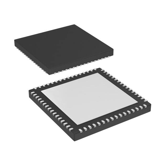


 工商网监
湘ICP备2023018690号
工商网监
湘ICP备2023018690号

