MCP16502
High-Performance PMIC for SAMA5DX/SAM9X6 MPUs
Features
Description
• Input Voltage: 2.7V to 5.5V
• Four 1A Output Current Buck Channels with
100% Maximum Duty Cycle Capability
• 2 MHz Buck Channels PWM Operation
• Two Auxiliary 300 mA Low-Dropout Linear
Regulators (LDOs)
• ±1% Voltage Accuracy for DDR (Buck2 Output),
Core (Buck3 Output) and CPU (Buck4 Output)
• Pin-Selectable Output Voltages for Buck2:
1.2V, 1.35V, 1.8V
• MPU-Specific Built-in Default Channel
Sequencing and nRSTO Assertion Delay
• Support of Hibernate, Low-Power and
High-Performance Modes with DVS
• Push Button Long Press Time-out Function
• 1 MHz I2C Interface for Programming and
Diagnostics
• Low Noise, Forced PWM (FPWM) and Low IQ,
Light Load, High-Efficiency Mode Available
• I2C-Selectable Displacement (±16.5%) of PWM
Switching Frequency
• Leakage-Free Interfacing to MPU in Any
Operating Condition through Optimized
ESD Protection
• Less than 300 µA Low-Power Mode Typical
Quiescent Current Bucks and LDO1 On, No Load
• 10 µA Maximum Shutdown Current (VIN = 4.5V,
TJ = +105°C)
• Cost and Size-Optimized BOM
• Thermal Shutdown and Current Limit Protection
• User-Programmable Overcurrent Fault Response
• 32-Pin 5 mm × 5 mm VQFN Package
• -40°C to +125°C Junction Temperature Range
The MCP16502 is an optimally integrated PMIC,
compatible with Microchip’s EMPUs (Embedded Microprocessor Units), requiring Dynamic Voltage Scaling
(DVS) with the use of High-Performance mode (HPM).
It is compatible with SAMA5DX and SAM9X6 MPUs,
which are supported by dedicated device variants that
optimize the solution BOM.
Applications
• High-Performance MPUs Power Supply Solutions
• µC/µP, FPGA and DSP Power
2019 Microchip Technology Inc.
The MCP16502 integrates four DC-DC Buck regulators
and two auxiliary LDOs, and provides a comprehensive
interface to the MPU, which includes an interrupt flag
and a 1 MHz I2C interface.
All Buck channels can support loads up to 1A and are
100% duty cycle-capable.
Two 300 mA LDOs are provided such that sensitive
analog loads can be supported.
The DDR memory voltage (Buck2 output) is selectable
by means of a 3-state input pin. This method allows
greater precision in the output voltage setting by eliminating inaccuracies due to external feedback resistors,
while minimizing external component count. The
voltage selection set allows easy migration across
different generations of memory.
The default power channel sequencing is built-in
according to the requirements of the MPU. A dedicated
pin (LPM) facilitates the transition to Low-Power modes
and the implementation of Backup mode with DDR in
self-refresh (Hibernate mode).
The MCP16502 features a low no-load operational
quiescent current and it draws less than 10 µA in full
shutdown.
Active discharge resistors are provided on each output.
All Buck channels support safe start-up into pre-biased
outputs.
The MCP16502 is available in a 32-pin 5 mm x 5 mm
VQFN package with an operating junction temperature
range from -40°C to +125°C.
DS20006275B-page 1
�MCP16502
OUT4
PVIN4
SW4
PGND4
PGND3
SW3
PVIN3
OUT3
Package Types
32
31
30
29
28
27
26
25
nINTO
1
24
nSTRT
nRSTO
2
23
HPM
SGND
3
22
LPM
SVIN
4
21
LOUT2
EP
19
LOUT1
nSTRTO
7
18
SELVL1
PWRHLD
8
17
SELV2
10
11
12
13
14
15
16
OUT2
OUT1
9
PVIN2
6
SW2
SCL
PGND2
LVIN
PGND1
20
SW1
5
PVIN1
SDA
32-Pin 5 mm x 5 mm VQFN – Top View
DS20006275B-page 2
2019 Microchip Technology Inc.
�MCP16502
Typical Application Circuit
VDDIODDR
VDDIOP[0,1,2]
VDDISC
VDDSDMMC
VDDUTMII
VDDBU
VDDOSC
VDDAUDIOPLL
VDDANA
VOUT4
1.8V
VIN : 2.7V-5.5V
VOUT2 (DDR) SUPPLY
VOLTAGE SELECTION
VIN
VIN
PVIN2
SELV2
LPDDR2
PGND2
MCP16502AC
VIN
C6
4.7 μF
L2
1.5-2.2 μH
C2
22 μF
SW2
VBAT
BACKUP SUPPLY
(BATTERY
or SUPERCAP)
R6
VOUT2
1.2V/1A
OUT2
VIN
Q1
PVIN1
PIOBU0
LPM
PGND1
SHDN
PWRHLD
C4
4.7 μF
L1
1.5-2.2 μH
C1
22 μF
SW1
3.3V/1A
HPM
OUT1
SAMA5D2
EMPU
VBAT
VIN
VOUT1
SVIN
R1
R2
R3
R4
R5
WKUP0
nRST
GPIOy
SGND
nSTRTO
nRSTO
LOUT1
SDA
SDA
LOUT2
SCL
SCL
C12
4.7�ȝF
nSTRT
VDDFUSE
VIN
C3
22 μF
C7
4.7 μF
L3
1.5-2.2 μH
C10
2.2 μF4.7 μF
VLOUT2
3.3V/0.3A
VLOUT1 DEFAULT OUTPUT
VOLTAGE SELECTION
VIN
PVIN3
VOUT3
1.25V/1A
C11
2.2 μF4.7 μF
VIN
SELVL1
100ȍ
VLOUT1
1.8V-2.5V-3.3V/0.3A
VIN
LVIN
nINTO
VDDCORE
VDDPLLA
VDDHSIC
VDDUTMIC
C9
2.2 μF
PVIN4
PGND4
SW4
C8
4.7 μF
L4
1.5-2.2 μH
C4
22 μF
VOUT4
1.8V/1A
OUT4
Application Schematic of MCP16502AC with SAMA5D2 and LPDDR2 (Wireless SOM Application)
2019 Microchip Technology Inc.
DS20006275B-page 3
�MCP16502
Functional Block Diagram
PVIN1
Buck1
SGND
SVIN
40 kȍ
nSTRT
SW1
PGND1
OUT1
PWRHLD
PVIN2
Buck2
LPM
HPM
SW2
PGND2
OUT2
SELV2
SELVL1
nSTRTO
SYSTEM
CONTROL
Buck3
PVIN3
SW3
PGND3
OUT3
nINTO
PVIN4
Buck4
nRSTO
SW4
PGND4
LVIN
LDO2
SCL
LOUT1
LDO1
SDA
Serial Interface
OUT4
LOUT2
DS20006275B-page 4
2019 Microchip Technology Inc.
�MCP16502
1.0
ELECTRICAL CHARACTERISTICS
Absolute Maximum Ratings†
SVIN to SGND .............................................................................................................................................. -0.3V to +6V
Power Supply Voltage Pins PVINx to PGNDx .............................................................................................. -0.3V to +6V
Power Supply Voltage Pins PVINx to SVIN ............................................................................................... -0.3V to +0.3V
OUTx Sense Pins to SGND .............................................................................................. ............................-0.3V to +6V
LVIN to SGND ................................................................................................................................. -0.3V to VSVIN + 0.3V
Output Switch Voltage SWx to PGNDx ..........................................................................................-0.3V to VPVINx + 0.3V
PGNDx to SGND ....................................................................................................................................... -0.3V to +0.3V
nSTRT, SELV2, SELVL1 to SGND ................................................................................................. -0.3V to VSVIN + 0.3V
SDA, SCL, LPM, HPM, PWRHLD, nRSTO, nSTRTO, nINTO to SGND....................................................... -0.3V to +6V
Maximum Junction Temperature................................................................................................. ............................150°C
Storage Temperature ............................................................................................................................. -65°C to +150°C
ESD Protection on All Pins:
HBM ..................................................................................................................................................................... 2 kV
MM ......................................................................................................................................................................200V
CDM ................................................................................................................................................................ 1000V
† Notice: Stresses above those listed under “Absolute Maximum Ratings” may cause permanent damage to the
device. This is a stress rating only and functional operation of the device at those or any other conditions above
those indicated in the operational listings of this specification is not intended. Exposure to maximum rating
conditions for extended periods may affect device reliability.
AC/DC CHARACTERISTICS
Electrical Specifications: Unless otherwise specified: TA = TJ = +25°C; VIN = SVIN = PVINx = LVIN = 5V; L1 = L2 = L3 = L4 = 2.2 µH;
COUT1, COUT2,, COUT3, COUT4 = 22 µF. Boldface type applies for junction temperatures TJ of -40°C to +125°C.
Parameters
Sym.
Min.
Typ.
Max.
Units
Supply Voltage Range
VIN
Undervoltage Lockout
Threshold
VUVLO_TH
Undervoltage Lockout
Hysteresis
Shutdown (Off) Current
Conditions
2.7
—
5.5
V
2.4
2.55
2.7
V
VUVLO_HYS
—
125
ISHDN
—
7
11
µA
PWRHLD = LPM = HPM = 0,
nSTRT, nRSTO, nSTRTO, nINTO
floating, VIN = 5.5V
ISHDN_105 (1)
—
6
10
µA
PWRHLD = LPM = HPM = 0,
nSTRT, nRSTO, nSTRTO, nINTO
floating, VIN = 4.5V,
TJ = -40°C to +105°C
Hibernate Mode
Non-Switching Quiescent
Current
IQNS_HIB
—
120
150
µA
IOUT2 = 0 mA, Buck2 on,
all other channels off,
VOUT2 > VOUT2_NOM,
LPM = 1, PWRHLD = HPM = 0
Hibernate Mode
Operational Quiescent
Current (Switching, One
Buck Channel On) (Note 2)
IQOP_HIB1
—
120
—
µA
IOUT2 = 0 mA, Buck2 on
(VOUT2 = 1.2V),
all other channels off, LPM = 1,
PWRHLD = HPM = 0
System Input Supply
Note 1:
2:
3:
4:
Turn-on
mV
Maximum limit for TJ = -40°C to +105°C based on characterization data.
Not production tested.
Typical value from bench characterization, maximum value production tested.
Input filters on the SDA and SCL inputs suppress noise spikes of less than 50 ns.
2019 Microchip Technology Inc.
DS20006275B-page 5
�MCP16502
AC/DC CHARACTERISTICS (CONTINUED)
Electrical Specifications: Unless otherwise specified: TA = TJ = +25°C; VIN = SVIN = PVINx = LVIN = 5V; L1 = L2 = L3 = L4 = 2.2 µH;
COUT1, COUT2,, COUT3, COUT4 = 22 µF. Boldface type applies for junction temperatures TJ of -40°C to +125°C.
Parameters
Sym.
Min.
Typ.
Max.
Units
Conditions
Hibernate Mode
Operational Quiescent
Current (Switching, Two
Buck Channels On) (Note 2)
IQOP_HIB2
—
165
—
µA
IOUT2 = IOUT4 = 0 mA,
Buck2 and Buck4 on
(VOUT2 = 1.2V, VOUT4 = 1.8V),
all other channels off, LPM = 1,
PWRHLD = HPM = 0
Low-Power Mode
Operational Quiescent
Current (Switching) (Note 2)
IQOP_LPM
—
290
—
µA
IOUTx = 0 mA, all channels on
except LDO2, default settings,
PWRHLD = LPM = 1, HPM = 0
Active Mode
Operational Quiescent
Current (Switching)(Note 2)
IQOP_ACT
—
16
—
mA
IOUTx = 0 mA, all channels
enabled, default settings,
PWRHLD = 1, LPM = HPM = 0
High-Performance Active
Mode
Operational Quiescent
Current (Switching) (Note 2)
IQOP_HPM
—
16
—
mA
IOUTx = 0 mA, all channels
enabled, default settings,
PWRHLD = HPM = 1, LPM = 0
ACC_TB
-10
—
+10
%
FSD[1:0] = 00, 01
Time Base
Time Base Accuracy
Thermal Protection and Warning
Overtemperature Shutdown
Threshold (Note 2)
TTSD
—
160
—
°C
Bit TSD to ‘1’
Overtemperature Shutdown
Hysteresis (Note 2)
TTSD_HYS
—
20
—
°C
Bit TSD to ‘0’
Overtemperature Warning
Threshold (Note 2)
TTWR
—
135
—
°C
Bit TWR to ‘1’
Overtemperature Warning
Hysteresis (Note 2)
TTWR_HYS
—
10
—
°C
Bit TWR to ‘0’
Input Operating Voltage
Range
VPVIN1
2.7
—
5.5
V
Output Voltage Range
VOUT1
1.2
—
3.7
V
Vstep
—
50
—
mV
IPVIN1_SHDN
—
0.05
2
µA
Regulator disabled, VPVIN1 = 5V
Operational Quiescent
Current, Auto-PFM, Default
Setting (Note 2)
IQOP_PFM1
—
45
—
µA
IOUT1 = 0 mA, Auto-PFM,
PWRHLD = LPM = 1, HPM = 0,
B1HCEN = 0 (default),
ΔIQ for Buck1 activated
Operational Quiescent
Current, Auto-PFM + HCM
(Note 2)
IQOP_HCM
—
47
—
µA
Output Voltage Accuracy,
FPWM
ACC_OUTPWM1
-2
—
+2
%
IOUT1 = 0 mA, Auto-PFM,
PWRHLD = LPM = 1, HPM = 0,
B1HCEN = 1,
ΔIQ for Buck1 activated
IOUT1 = 0 mA
Output Voltage Accuracy,
Auto-PFM
ACC_OUTPFM1
-2
—
+2
%
IOUT1 = 0 mA, B1HCEN = 0
Buck1
Output Voltage Step
PVIN1 Shutdown Current
Note 1:
2:
3:
4:
50 mV steps
Maximum limit for TJ = -40°C to +105°C based on characterization data.
Not production tested.
Typical value from bench characterization, maximum value production tested.
Input filters on the SDA and SCL inputs suppress noise spikes of less than 50 ns.
DS20006275B-page 6
2019 Microchip Technology Inc.
�MCP16502
AC/DC CHARACTERISTICS (CONTINUED)
Electrical Specifications: Unless otherwise specified: TA = TJ = +25°C; VIN = SVIN = PVINx = LVIN = 5V; L1 = L2 = L3 = L4 = 2.2 µH;
COUT1, COUT2,, COUT3, COUT4 = 22 µF. Boldface type applies for junction temperatures TJ of -40°C to +125°C.
Parameters
Sym.
Min.
Typ.
Max.
Units
Conditions
LINE_REGPWM1
—
0.03
—
%
LINE_REGPFM1
—
0.07
—
IOUT1 = 0 mA, FPWM,
VIN = PVIN1 = SVIN = 3.6V to 5.5V
IOUT1 = 0 mA, Auto-PFM,
VIN = PVIN1 = SVIN = 3.6V to 5.5V
LOAD_REGPWM1
—
0.3
—
%
IOUT1 = 0A to 1A, FPWM
LOAD_REGPFM1
—
0.5
—
%
IOUT1 = 0A to 1A, Auto-PFM
Hysteretic Control Mode
Upper Regulation Threshold,
Auto-PFM
HCM_TH
1.7
2.9
4.3
%
IOUT1 = 0 mA,
PWRHLD = LPM = 1, HPM = 0,
B1HCEN = 1,
SVIN = PVIN1 = 1.06, VOUT1_NOM,
OUT1 rising, % of VOUT1_NOM
Hysteretic Control Mode
Disable Threshold,
Auto-PFM
HCM_DIS
—
11.1
—
%
IOUT1 = 0 mA,
PWRHLD = LPM = 1, HPM = 0,
B1HCEN = 1, SVIN = PVIN1 rising,
% of VOUT1_NOM
Hysteretic Control Mode
Enable Threshold,
Auto-PFM
HCM_EN
5
9
13
%
IOUT1 = 0 mA,
PWRHLD = LPM = 1, HPM = 0,
B1HCEN = 1, SVIN = PVIN1 falling,
% of VOUT1_NOM
Switching Frequency
fsw
1.8
2
2.2
MHz
Switching Frequency
Displacement
FSD_10
—
-16.5
—
%
FPWM, FSD[1:0] = 10
FSD_11
—
+16.5
—
%
Maximum Duty Cycle
DMAX
100
—
—
%
FPWM, FSD[1:0] = 11
Functionality test
Minimum On Time
TON_MIN1
—
35
—
ns
FPWM
High-Side Switch
On-Resistance
RDsonP1
—
140
160
mΩ
PVIN1 = SVIN = 3.6V
Low-Side Switch
On-Resistance
RDsonN1
—
120
140
mΩ
PVIN1 = SVIN = 3.6V
Output Voltage Line
Regulation (Note 2)
Output Voltage Load
Regulation (Note 2)
POK (Power OK) Threshold
FPWM, FSD[1:0] = 00, 01
POK_TH1
90
92.5
95
%
OUT1 rising, % of VOUT1_NOM
POK Hysteresis
POK_HYS1
—
4
—
%
OUT1 falling, % of VOUT1_NOM
Start-up POK Bypass
Threshold
VPOKB_TH_B1
360
400
440
mV
PVIN1 – OUT1, OUT1 rising,
PVIN1 = 3.0V, VOUT1_NOM = 3.3V
Start-up POK Bypass
Threshold Hysteresis
VPOKB_HYS_B1
—
50
—
mV
OUT1 falling, PVIN1 = 3.0V
SSR_00
—
16
—
Soft Start Rate
(Switching Frequency Clock
Cycles per DAC Step)
SSR_01
—
32
—
cycles/ SSR[1:0] = 00 (default)
step
SSR[1:0] = 01
SSR_10
—
48
—
SSR[1:0] = 10
SSR_11
—
64
—
Dynamic Voltage Scaling
Rate
(Switching Frequency
Clock Cycles Per DAC
Step)
DVSR_00
16
DVSR_01
32
SSR[1:0] = 11
cycles/ DVSR[1:0] = 00 (default)
step
DVSR[1:0] = 01
DVSR_10
48
DVSR[1:0] = 10
DVSR_11
64
DVSR[1:0] = 11
High-Side Peak Current
Limit (Cycle by Cycle)
ILIM_HS1
Note 1:
2:
3:
4:
1.2
1.8
2.4
A
Maximum limit for TJ = -40°C to +105°C based on characterization data.
Not production tested.
Typical value from bench characterization, maximum value production tested.
Input filters on the SDA and SCL inputs suppress noise spikes of less than 50 ns.
2019 Microchip Technology Inc.
DS20006275B-page 7
�MCP16502
AC/DC CHARACTERISTICS (CONTINUED)
Electrical Specifications: Unless otherwise specified: TA = TJ = +25°C; VIN = SVIN = PVINx = LVIN = 5V; L1 = L2 = L3 = L4 = 2.2 µH;
COUT1, COUT2,, COUT3, COUT4 = 22 µF. Boldface type applies for junction temperatures TJ of -40°C to +125°C.
Parameters
Sym.
Min.
Typ.
Max.
Units
Current Limit Frequency
Foldback VOUT1 Threshold
VTH_FFB1
—
500
—
mV
Hiccup Mode Short-Circuit
Protection Wait Time
tHICCUP
—
3x Soft
Start Time
—
ILIM_NEG1
-1.4
-1
-0.8
A
Zero Current Detection
Threshold
IZCD1
0
50
110
mA
Active
Discharge Resistance
RDISCH_OUT1
—
25
—
Ω
Input Operating Voltage
Range
VPVINx
2.7
—
5.5
V
Output Voltage Range
VOUTx
0.6
—
1.85
V
Low-Side Negative Peak
Current Limit (FPWM)
Conditions
DISCH = 1, enabled when
regulator is disabled
Buck2, Buck3, Buck4
Output Voltage Step
25 mV steps
Vstep
—
25
—
mV
IPVINx_SHDN
—
0.05
2
µA
Regulator disabled, PVINx = 5V
IQOP_PFMx
—
45
—
µA
IOUTx = 0 mA, Auto-PFM,
PWRHLD = LPM = 1, HPM = 0,
ΔIQ for one Buck activated
Output Voltage Accuracy,
FPWM
ACC_OUTPWMx
-1
—
+1
%
IOUTx = 0 mA, 0.9V ≤ VOUTx ≤ 1.3V
-1.5
—
+1.5
Output Voltage Accuracy,
Auto-PFM
ACC_OUTPFMx
Output Voltage Line
Regulation (Note 2)
PVINx Shutdown Current
Operational Quiescent
Current, Auto-PFM (Note 2)
Output Voltage Load
Regulation (Note 2)
-1
—
+1
-1.5
—
+1.5
LINE_REGPWMx
—
0.03
—
LINE_REGPFMx
—
0.07
—
LOAD_REGPWMx
—
0.3
—
LOAD_REGPFMx
—
0.5
—
IOUTx = 0 mA, VOUTx < 0.9V or
VOUTx > 1.3V
%
IOUTx = 0 mA, 0.9V ≤ VOUTx ≤ 1.3V
IOUTx = 0 mA, VOUTx < 0.9V or
VOUTx > 1.3V
%
IOUT1 = 0 mA, FPWM,
VIN = PVIN1 = SVIN = 3.6V to 5.5V
IOUT1 = 0 mA, Auto-PFM,
VIN = PVIN1 = SVIN = 3.6V to 5.5V
%
IOUTx = 0A to 1A, FPWM
IOUTx = 0A to 1A, Auto-PFM
Switching Frequency
fsw
1.8
2
2.2
MHz
Switching Frequency
Displacement
FSD_10
—
-16.5
—
%
FPWM, FSD[1:0] = 10
FSD_11
—
16.5
—
%
Maximum Duty Cycle
DMAX
100
—
—
%
FPWM, FSD[1:0] = 11
Functionality test
Minimum On Time
TON_MINx
—
35
—
ns
FPWM
High-Side Switch
On-Resistance
RDSonPx
—
140
160
mΩ
PVINx = SVIN = 3.6V
Low-Side Switch
On-Resistance
RDSonNx
—
120
140
mΩ
PVINx = SVIN = 3.6V
POK_THx
90
92.5
95
%
OUTx rising, % of VOUTx(NOM)
POK_HYSx
—
4
—
%
OUTx falling, % of VOUTx(NOM)
POK (Power OK) Threshold
POK Hysteresis
Note 1:
2:
3:
4:
FPWM, FSD[1:0] = 00, 01
Maximum limit for TJ = -40°C to +105°C based on characterization data.
Not production tested.
Typical value from bench characterization, maximum value production tested.
Input filters on the SDA and SCL inputs suppress noise spikes of less than 50 ns.
DS20006275B-page 8
2019 Microchip Technology Inc.
�MCP16502
AC/DC CHARACTERISTICS (CONTINUED)
Electrical Specifications: Unless otherwise specified: TA = TJ = +25°C; VIN = SVIN = PVINx = LVIN = 5V; L1 = L2 = L3 = L4 = 2.2 µH;
COUT1, COUT2,, COUT3, COUT4 = 22 µF. Boldface type applies for junction temperatures TJ of -40°C to +125°C.
Parameters
Sym.
Min.
Typ.
Max.
Units
Conditions
Soft Start Rate
(Switching Frequency Clock
Cycles per DAC Step)
SSR_00
—
16
—
SSR_01
—
32
—
cycles/ SSR[1:0] = 00 (default)
step
SSR[1:0] = 01
SSR_10
—
48
—
SSR[1:0] = 10
SSR_11
—
64
—
DVSR_00
—
16
—
DVSR_01
—
32
—
SSR[1:0] = 11
cycles/ DVSR[1:0] = 00 (default)
step
DVSR[1:0] = 01
DVSR_10
—
48
—
DVSR[1:0] = 10
DVSR_11
—
64
—
High-Side Peak Current
Limit (Cycle-by-Cycle)
ILIM_HSx
1.2
1.8
2.4
A
Current Limit Frequency
Foldback VOUTx Threshold
VTH_FFBx
—
500
—
mV
Hiccup Mode Short-Circuit
Protection Wait Time
tHICCUP
—
3x Soft
Start Time
—
ILIM_NEGx
-1.4
-1
-0.8
A
IZCDx
0
33
110
mA
RDISCH_OUTx
—
25
—
Ω
VLVIN
2.7
—
5.5
V
VLOUTx
1.2
—
3.7
V
Vstep
—
50
—
mV
CLOUTx
2.2
—
20
µF
ILOUT1,2 ≤ 150 mA – application
requirement
4.7
—
20
µF
ILOUT1,2 ≤ 300 mA – application
requirement
Dynamic Voltage Scaling
Rate
(Switching Frequency Clock
Cycles per DAC Step)
Low-Side Negative Peak
Current Limit (FPWM)
Zero Current Detection
Threshold
Active Discharge
Resistance
DVSR[1:0] = 11
DISCH = 1, enabled when
regulator is disabled
LDO1, LDO2
Input Operating Voltage
Range
Output Voltage Range
Output Voltage Step
Stable Output Capacitor
Range (Note 2)
LVIN Shutdown Current
ILVIN_SHDN
—
—
2
µA
LDOs disabled, LVIN = 5V
Operational Quiescent
Current
ILVIN_Qx
—
40
—
µA
ILOUT1,2 = 0 mA, one LDO block
ACC_LOUTx
-3
—
+3
%
LVIN = SVIN = 3.6V,
ILOUT1,2 = 0.1 mA
Output Voltage Accuracy
Dropout Voltage (Note 3)
VDOx
—
170
500
mV
ILOUT1,2 = 300 mA
Output Voltage Line
Regulation
LINE_REGx
—
0.024
—
%
LVIN = SVIN = 3.6V to 5.5V,
ILOUT1,2 = 0.1 mA
Output Voltage Load
Regulation
LOAD_REGx
—
0.3
—
%
ILOUT1,2 = 0.1 mA to 300 mA
Note 1:
2:
3:
4:
Maximum limit for TJ = -40°C to +105°C based on characterization data.
Not production tested.
Typical value from bench characterization, maximum value production tested.
Input filters on the SDA and SCL inputs suppress noise spikes of less than 50 ns.
2019 Microchip Technology Inc.
DS20006275B-page 9
�MCP16502
AC/DC CHARACTERISTICS (CONTINUED)
Electrical Specifications: Unless otherwise specified: TA = TJ = +25°C; VIN = SVIN = PVINx = LVIN = 5V; L1 = L2 = L3 = L4 = 2.2 µH;
COUT1, COUT2,, COUT3, COUT4 = 22 µF. Boldface type applies for junction temperatures TJ of -40°C to +125°C.
Parameters
Sym.
Min.
Typ.
Max.
Units
PSRRx
—
63
—
dB
f = 1 kHz, IOUT = 20 mA,
VLOUT1,2 = 1.8V, SVIN and LVIN
modulated
—
63
—
dB
f = 1 kHz, IOUT = 20 mA,
VLOUT1,2 = 1.8V, SVIN = 5V,
LVIN modulated
—
46
—
dB
f = 10 kHz, IOUT = 20 mA,
VLOUT1,2 = 1.8V, SVIN and LVIN
modulated
—
47
—
dB
f = 10 kHz, IOUT = 20 mA,
VLOUT1,2 = 1.8V, SVIN = 5V,
LVIN modulated
POK_THL
90
92.3
95
%
LOUT1,2 rising,
% of VLOUT1,2(NOM)
POK Hysteresis
POK_HYSL
—
4
—
%
LOUT1,2 falling,
% of VLOUT1,2(NOM)
Start-up POK Bypass
Threshold
VPOKB_TH_Lx
400
500
600
mV
LVIN – LOUTx, LOUTx rising,
LVIN = 3.0V, VLOUTx_NOM = 3.3V
Start-up POK Bypass
Threshold Hysteresis
(Note 2)
VPOKB_HYS_Lx
—
50
—
mV
LOUTx falling, LVIN = 3.0V
SSR_00
—
16
—
SSR_01
—
32
—
cycles/ SSR[1:0] = 00 (default)
step
SSR[1:0] = 01
SSR_10
—
48
—
SSR[1:0] = 10
SSR_11
—
64
—
Dynamic Voltage Scaling
Rate
(Switching Frequency Clock
Cycles per DAC Step) –
Rising Only
DVSR_00
—
16
—
DVSR_11
—
64
—
Current Limit
ILIM_LOUTx
310
420
550
mA
RDISCH_LOUTx
—
25
—
Ω
DISCH = 1, enabled when
regulator is disabled and during
negative DVS
Logic High Input Voltage,
VIH
VIH_nSTRT
0.66 VSVIN
—
—
V
SVIN = 3.6V-5.5V
Logic Low Input Voltage,
VIL
VIL_nSTRT
—
—
0.36 VSVIN
V
SVIN = 3.6V-5.5V
Pull-up Resistance
RPU_nSTRT
—
40
—
kΩ
nSTRT Deglitch Time
tDT_nSTRT
—
10
—
µs
PSRR (Note 2)
POK (Power OK) Threshold
Soft Start Rate
(Switching Frequency Clock
Cycles per DAC Step)
Active Discharge
Resistance
Conditions
DVSR_01
—
32
—
SSR[1:0] = 11
cycles/ DVSR[1:0] = 00 (default)
step
DVSR[1:0] = 01
DVSR_10
—
48
—
DVSR[1:0] = 10
DVSR[1:0] = 11
SVIN = LVIN = 4.5V,
VLOUT1,2 = 80% of nominal
nSTRT Input
Note 1:
2:
3:
4:
Falling edge of nSTRT pin
Maximum limit for TJ = -40°C to +105°C based on characterization data.
Not production tested.
Typical value from bench characterization, maximum value production tested.
Input filters on the SDA and SCL inputs suppress noise spikes of less than 50 ns.
DS20006275B-page 10
2019 Microchip Technology Inc.
�MCP16502
AC/DC CHARACTERISTICS (CONTINUED)
Electrical Specifications: Unless otherwise specified: TA = TJ = +25°C; VIN = SVIN = PVINx = LVIN = 5V; L1 = L2 = L3 = L4 = 2.2 µH;
COUT1, COUT2,, COUT3, COUT4 = 22 µF. Boldface type applies for junction temperatures TJ of -40°C to +125°C.
Parameters
Sym.
Min.
Typ.
Max.
Units
Conditions
SELV2, SELVL1 Three-State Inputs (x = 2, L1)
High State Threshold
Voltage, VIHT
VIHT_SELVx
VSVIN – 0.9V
—
VSVIN – 0.4V
V
Low State Threshold
Voltage, VILT
VILT_SELVx
0.5
—
1.0
V
Input Leakage Current High
IlkgH_SELVx
—
0.01
1
µA
SELVx = SVIN – 0.4V
Input Leakage Current Low
IlkgL_SELVx
-1
0.01
—
µA
SELVx = 0.4V
V
SVIN = 3.6V-5.5V
SVIN = 3.6V-5.5V
PWRHLD, LPM, HPM Logic Inputs (x= PWRHLD, LPM, HPM)
Logic High Input Voltage,
VIH
VIH_x
1.5
—
—
Logic Low Input Voltage, VIL
VIL_x
—
—
0.4
V
Input Leakage Current
Ilkg_x
-1
—
1
µA
Deglitch Time
tDT_x
—
10
—
µs
nRSTO, nSTRTO, nINTO Logic Outputs (x = nRSTO, nSTRTO, nINTO)
Output Voltage Low, VOL
VOL_x
—
—
0.4
V
SVIN = 3.6V-5.5V, IOL = 2 mA
Leakage Current
Ilkg_x
—
—
1
µA
5.5V applied, output driver off
SDA, SCL I2C Interface Pins (x = SDA, SCL)
SCL, SDA Logic High Input
Voltage, VIH
VIH_x
1.5
—
—
V
SVIN = 3.6V-5.5V
SCL, SDA Logic Low Input
Voltage, VIL
VIL_x
—
—
0.4
V
SVIN = 3.6V-5.5V
Hysteresis of Schmitt
Trigger Inputs
Vhys_x
—
0.2
—
V
SVIN = 3.6V-5.5V
SDA, SCL Leakage Current
Ilkg_x
—
—
1
µA
SDA driver off, VSDA = 5.5V,
VSCL= 5.5V
SDA Output Voltage Low,
VOL
VOL
—
—
0.4
V
SVIN = 3.6V-5.5V, IOL = 20 mA
Maximum SCL Clock
Frequency
fSCL
—
1
—
MHz
Functional test only
Maximum Pulse Width of
Input Spikes that Must be
Suppressed (Notes 2, 4)
tSP
—
50
—
ns
Functional test only
Note 1:
2:
3:
4:
Maximum limit for TJ = -40°C to +105°C based on characterization data.
Not production tested.
Typical value from bench characterization, maximum value production tested.
Input filters on the SDA and SCL inputs suppress noise spikes of less than 50 ns.
TEMPERATURE SPECIFICATIONS(1)
Parameters
Sym.
Min.
Typ.
Max.
Units
Conditions
Operating Junction Temperature
Range
TJ
-40
—
+125
°C
Steady state
Maximum Junction Temperature
TJ_MAX
—
—
+150
°C
Transient
θJA
—
25.8
—
°C/W
Temperature Ranges
Package Thermal Resistance
Note 1:
TA = +25°C; VIN = SVIN = PVINx = LVIN = 5V; unless otherwise specified.
Bold values indicate -40°C ≤ TJ ≤ +125°C.
2019 Microchip Technology Inc.
DS20006275B-page 11
�MCP16502
2.0
TYPICAL PERFORMANCE CURVES
Note:
The graphs and tables provided following this note are a statistical summary based on a limited number of
samples and are provided for informational purposes only. The performance characteristics listed herein
are not tested or guaranteed. In some graphs or tables, the data presented may be outside the specified
operating range (e.g., outside specified power supply range) and therefore outside the warranted range.
180
VIN Operating Current (μA)
V2872� = 1.2V
170
TA = 125°C
V2874� = 1.8V
Efficiency (%)
160
TA = 105°C
150
140
TA = 25°C
130
TA = -40°C
120
110
100
2.7
3.1
3.5
3.9
4.3
4.7
Input Voltage (V)
5.1
VIN Operating Current (μA)
B1HCEN = '0'
Efficiency (%)
B1HCEN = '1'
500
400
TA = 125°C TA = 105°C
TA = 25°C
300
TA = -40°C
200
2.7
3.1
3.5
3.9
4.3
4.7
Input Voltage (V)
5.1
VIN Operating Current (mA)
Efficiency (%)
TA = 125°C
14
TA = 25°C
12
TA = -40°C
10
8
6
2.7
3.1
3.5
3.9
4.3
4.7
Input Voltage (V)
5.1
5.5
FIGURE 2-3:
VIN Quiescent Current vs.
Input Voltage and Temperature – Active Mode
(LPM = Low, PWRHLD = High, HPM = Low).
DS20006275B-page 12
100.0
1000.0
AUTO�PFM
1.0
10.0
IOUT (mA)
100.0
1000.0
FIGURE 2-5:
Buck2 Efficiency vs. Load
Current (VOUT2 = 1.2V).
18
TA = 105°C
10.0
IOUT (mA)
VIN = 5V
FPWM
0.1
20
16
1.0
100
90
80
70
60
50
40
30
20
10
0
5.5
FIGURE 2-2:
VIN Quiescent Current vs.
Input Voltage and Temperature – Low-Power
Mode (LPM = PWRHLD = High, HPM = Low).
AUTO�PFM
FIGURE 2-4:
Buck1 Efficiency vs. Load
Current (VOUT1 = 3.3V).
800
600
VIN = 5V
FPWM
0.1
5.5
FIGURE 2-1:
VIN Operating Current vs.
Input Voltage and Temperature – Hibernate
Mode (LPM = High, PWRHLD = HPM = Low).
700
100
90
80
70
60
50
40
30
20
10
0
100
90
80
70
60
50
40
30
20
10
0
VIN = 5V
FPWM
AUTO�PFM
0.1
1.0
10.0
IOUT (mA)
100.0
1000.0
FIGURE 2-6:
Buck3 Efficiency vs. Load
Current (VOUT3 = 1.25V).
2019 Microchip Technology Inc.
�100
90
80
70
60
50
40
30
20
10
0
0.20
0.19
0.18
0.17
0.16
0.15
0.14
0.13
0.12
0.11
0.10
VIN = 5V
FPWM
AUTO�PFM
0.1
1.0
10.0
IOUT (mA)
100.0
VIN = 5V
Buck2: VOUT2 = 1.8V
VIN = 3.6V
Buck3: VOUT3 = 1.25V VIN = 3.3V
2.05
2.00
Buck1
Buck2
1.95
1.90
Buck3
Output Voltage (V)
Switching Frequency (MHz)
2.10
Buck1: VOUT1 = 3.3V
1.85
1.80
-40 -25 -10
3.310
3.305
3.300
3.295
3.290
3.285
3.280
3.275
3.270
3.265
3.260
5 20 35 50 65 80 95 110 125
Ambient Temperature (°C)
MOSFET RDS(ON) vs.
VIN = 5V
TA = -40°C
TA = 25°C
TA = 125°C
0
5 20 35 50 65 80 95 110 125
Ambient Temperature (°C)
FIGURE 2-8:
Switching Frequency vs.
Temperature – Active Mode (LPM = Low,
PWRHLD = High, HPM = Low).
1.260
N-MOS
FIGURE 2-10:
Temperature.
2.20
2.15
P-MOS
-40 -25 -10
1000.0
FIGURE 2-7:
Buck4 Efficiency vs. Load
Current (VOUT3 = 1.8V).
50
100
150
200
Output Current (mA)
250
300
FIGURE 2-11:
LDO1 Output Voltage vs.
Output Current and Temperature (Load
Regulation – VLOUT1 = 3.3V).
1.810
VIN = 5V
VOUT3 = 1.25V VIN = 5V
1.805
Output Voltage (V)
1.255
Output Voltage (V)
VIN = 5V
RDS(ON) (Ω)
Efficiency (%)
MCP16502
1.250
1.245
1.240
1.800
1.795
TA = -40°C
1.790
1.785
1.235
1.780
1.230
1.775
TA = 25°C
TA = 125°C
-40 -25 -10 5 20 35 50 65 80 95 110 125
Ambient Temperature (°C)
FIGURE 2-9:
Buck3 Output Voltage vs.
Temperature – VOUT3 = 1.25V, Active Mode
(LPM = Low, PWRHLD = High, HPM = Low).
2019 Microchip Technology Inc.
0
50
100
150
200
Output Current (mA)
250
300
FIGURE 2-12:
LDO2 Output Voltage vs.
Output Current and Temperature (VLOUT2 = 1.8V).
DS20006275B-page 13
�MCP16502
180
Dropout Voltage (mV)
160
LDO2
LPM=’0’
PWRHLD
140
LDO1
120
VOUT1 (3.3V)
2V/div
100
80
VOUT2 (1.8V)
2V/div
60
40
VOUT3 (1.2V)
2V/div
nRSTO
5V/div
20
0
0
50
100
150
200
Output Current (mA)
250
300
FIGURE 2-13:
LDO1, LDO2 Dropout
Voltage vs. Load Current.
800 s/div
FIGURE 2-16:
Sequence.
PWRHLD Shutdown
LPM=’1’
PWRHLD
PWRHLD= ‘1’
nSTRT
VOUT1 (3.3V)
2V/div
VOUT1 (3.3V)
2V/div
VOUT2 (1.8V)
2V/div
VOUT2 (1.8V)
2V/div
VOUT3 (1.25V)
2V/div
nRSTO
5V/div
VOUT3 (1.25V)
2V/div
nRSTO
800 s/div
4 ms/div
FIGURE 2-14:
nSTRT Start-up Sequence.
FIGURE 2-17:
Entering Hibernate Mode.
VOUT3 (1.25V)
AC Coupled
VOUT3= 1.2V
20AC
mV/div
Coupled
LPM=’0’
PWRHLD
20 mV/div
VOUT1 (3.3V)
2V/div
VOUT2 (1.8V)
1V/div
VOUT3 (1.25V)
1V/div
nRSTO
5V/div
DS20006275B-page 14
500 mA
2 mA
4 ms/div
FIGURE 2-15:
Sequence.
IOUT3
IOUT3
500 mA/div
mA/div
500
PWRHLD Start-up
40 s/div
Buck3 Transient
FIGURE 2-18:
Response (Active Mode, VOUT3 = 1.25V).
2019 Microchip Technology Inc.
�MCP16502
VOUT1
AC Coupled
10 mV/div
HPM
VOUT4 = 1.1V to 1.375V
500 mV/div
VOUT2
AC Coupled
10 mV/div
VOUT3 AC Coupled
VOUT4
AC Coupled
10 mV/div
SW4
10 mV/div
nRSTO
2 s/div
400 s/div
FIGURE 2-19:
Buck4 DVS Transition.
FIGURE 2-22:
Buck Channels Output
Voltage Ripple, Active (FPWM) Mode.
VOUT1
AC Coupled
20 mV/div
SHORT
CIRCUIT
IOUT1
5A/div
VOUT2
AC Coupled
20 mV/div
VOUT1(3.3V)
2V/div
SW1
VOUT3
AC Coupled
20 mV/div
nRSTO
4 ms/div
FIGURE 2-20:
Output Short Circuit on
VOUT1 – HCPEN = 1.
ILOUT1
200 mA/div
30 mA
VLOUT1
AC Coupled
50 mV/div
270 mA
40 ms/div
FIGURE 2-23:
Buck Channels Output
Voltage Ripple, Low-Power (Auto-PFM)
Mode.
LPM
PWRHLD
FAULT
nSTRTO
nRSTO
LDO2
LDO1
BUCK4
BUCK3
BUCK2
BUCK1
270 mA
IOUT2
200 mA/div
30 mA
VOUT2
AC Coupled
50 mV/div
VOUT4
AC Coupled
20 mV/div
20 ms/div
10 s/div
FIGURE 2-21:
LDO1, LDO2 Load
Transient Response.
2019 Microchip Technology Inc.
FIGURE 2-24:
Hibernate Mode.
Automatic Wake-up Pulse,
DS20006275B-page 15
�MCP16502
3.0
PIN DESCRIPTION
The descriptions of the pins are listed in Table 3-1.
TABLE 3-1:
PIN FUNCTION TABLE
Pin Name
Pin
Number
Description
1
nINTO
Active-Low, Open-Drain Interrupt Output.
2
nRSTO
Active-Low, Open-Drain Reset Output.
3
SGND
Signal Ground. Connect to reference ground plane.
4
SVIN
Input Voltage for the Analog Control Circuitry. Decouple SVIN to SGND with a 1 µF
(minimum) ceramic capacitor.
5
SDA
I2C Interface Serial Data.
6
SCL
I2C Interface Serial Clock.
7
nSTRTO
8
PWRHLD Power Hold Input. Typically asserted as high by the MPU to maintain power after the
initial start-up is triggered by nSTRT. PWRHLD is to be asserted as low by the MPU
to initiate a PMIC shutdown sequence.
Active-Low, Open-Drain Start Event Output. nSTRTO is asserted low whenever
nSTRT is low.
9
OUT1
Output Sensing for Buck Channel 1. Connect to the regulation point for VOUT1.
10
PVIN1
Power Input Voltage of Buck Channel 1. Connect a ceramic capacitor from PVIN1 to
the PGND1 pin, to localize pulsed current loops and decouple switching noise.
11
SW1
12
PGND1
Power Ground of Buck Channel 1.
13
PGND2
Power Ground of Buck Channel 2.
14
SW2
15
PVIN2
Power Input Voltage of Buck Channel 2. Connect a ceramic capacitor from PVIN2 to
the PGND2 pin to localize pulsed current loops and decouple switching noise.
16
OUT2
Output Sensing for Buck Channel 2. Connect to the regulation point for VOUT2.
Switch Node of Buck Channel 1. Internal power MOSFET switches and external
inductor connection.
Switch Node of Buck Channel 2. Internal power MOSFET switches and external
inductor connection.
17
SELV2
Buck Channel 2 Output Voltage Selection Pin. Three-state input.
18
SELVL1
LDO1 Default Output Voltage Selection Pin. Three-state input.
19
LOUT1
LDO1 Output. Decouple LOUT1 to ground with a 2.2 µF (minimum) ceramic capacitor.
Default start-up state is on. LDO1 can be disabled by I2C.
20
LVIN
21
LOUT2
LDO2 Output. If LDO2 is in use, decouple LOUT2 to SGND with a 2.2 µF (minimum)
ceramic capacitor.
22
LPM
Low-Power Mode Input Pin. In combination with PWRHLD and HPM, this pin defines
the power mode status of the MCP16502.
23
HPM
High-Performance Mode Input Pin. In combination with PWRHLD and LPM, this pin
defines the power mode status of the MCP16502. Connect to ground if not used.
24
nSTRT
Start Event Input. Drive nSTRT to low to initiate a start-up sequence. nSTRT is
pulled up internally. A capacitor can be connected to nSTRT to automatically initiate
a power-up sequence when the main supply rises.
25
OUT3
Output Sensing for Buck Channel 3. Connect to the regulation point for VOUT3.
26
PVIN3
Power Input Voltage of Buck Channel 3. Connect a ceramic capacitor from PVIN3 to
the PGND3 pin to localize pulsed current loops and decouple switching noise.
27
SW3
DS20006275B-page 16
Input Voltage for LDO1 and LDO2. Decouple LVIN to ground with a 2.2 µF
(minimum) ceramic capacitor.
Switch Node of Buck Channel 3. Internal power MOSFET switches and external
inductor connection.
2019 Microchip Technology Inc.
�MCP16502
TABLE 3-1:
PIN FUNCTION TABLE (CONTINUED)
Pin Name
Pin
Number
28
PGND3
Power Ground of Buck Channel 3.
29
PGND4
Power Ground of Buck Channel 4.
30
SW4
31
PVIN4
Power Input Voltage of Buck Channel 4. Connect a ceramic capacitor from PVIN4 to
the PGND4 pin to localize pulsed current loops and decouple switching noise.
32
OUT4
-
EP
Output Sensing for Buck Channel 4. Connect to the regulation point for VOUT4.
Exposed Pad. Connect to ground plane with vias to ensure good thermal properties.
2019 Microchip Technology Inc.
Description
Switch Node of Buck Channel 4. Internal power MOSFET switches and external
inductor connection.
DS20006275B-page 17
�MCP16502
4.0
DEVICE OPTIONS
The MCP16502 is offered in different options,
depending on the target MPU platform and external
memory type. The options currently available, also
shown in Table 4-1, are the following:
1.
MCP16502AA
This variant is intended for a high-performance (i.e.,
500 MHz) SAMA5D2 application; therefore, the voltage
of Buck3 (core voltage) is set to 1.25V by default.
Buck4 is typically not used by the SAMA5D2 MPU, so
it is disabled during the start-up sequence. If needed, it
can be turned on through I2C commands after the
start-up sequence has concluded.
Buck4 components can therefore be left not populated
if the end user does not need Buck4, thus saving board
space and BOM cost.
2.
MCP16502AB
This variant is intended for use cases where MPUs with
DVS support use ordinary DDRx memories.
3.
MCP16502AC
This variant is intended for an efficiency optimized,
high-performance (i.e., 500 MHz) SAMA5D2 application
with LPDDR2 memories.
Hibernate mode. LDO2 is not part of the start-up
sequence and is free for other purposes (turned on by
I2C command).
4.
MCP16502AD
This variant is intended for use cases where MPUs with
DVS support use LPDDRx memories.
5.
MCP16502AE
This variant is intended for the SAM9X6 MPU series.
Buck3 default voltage has been set to 1.15V to enable
600 MHz core and CPU operation.
Buck4 is excluded from the start-up sequence and is,
by default, off in any power state. Therefore, Buck4
external components can be removed if not needed,
thus saving overall cost and board space.
Buck4 components can also be populated and Buck4
can always be activated outside of the start-up
sequence by an I2C command.
The SAM9X6 series, just like its predecessor, SAM9X5
series, can ONLY support 1.8V memories (DDR2/
LPSDR/LPDDR). This implies that Buck2 should be set
accordingly.
Note:
Buck3 (core voltage) is therefore set to 1.25V for
500 MHz operation. Buck2 will be used for the 1.2V rail
of the LPDDR2, while Buck4 will be used for the 1.8V
rail of the LPDDR2 and will have a different sequencing
than in other variants. Buck2 should NOT be set to any
other voltage but 1.2V. Buck4 will also stay on during
TABLE 4-1:
All device variants are generated at the
factory with One-Time-Programmable
memory, which configures default settings
at power-up. Please contact your nearest
Microchip Sales Office for further assistance on the development of customized
device variants.
DEFAULT CONFIGURATIONS
Device
Options
MCP16502AA
MCP16502AB
MCP16502AC
MCP16502AD
MCP16502AE
VOUT1
3.3V
3.3V
3.3V
3.3V
3.3V
VOUT2
SELV2 Selectable
SELV2 Selectable
SELV2 Selectable
(set to 1.2V)
SELV2 Selectable
(set to 1.2V)
SELV2 Selectable
VOUT3
1.25V
1.15V
1.25V
1.15V
1.15V
Off
1.15V
1.8V
1.15V
Off
VOUT4
VLOUT1
SELVL1 Selectable SELVL1 Selectable SELVL1 Selectable SELVL1 Selectable SELVL1 Selectable
VLOUT2
Off
Off
Off
1.8V
Off
Platform
SAMA5D2
Reserved
SAMA5D2
with LPDDR2
Reserved
SAM9X6
DS20006275B-page 18
2019 Microchip Technology Inc.
�MCP16502
4.1
Buck Channels and Related
External Components
The MCP16502 Buck channels are based on Peak
Current mode control architecture and have internal
frequency compensation for the voltage regulation
loop. The slope compensation is optimized for inductors in the 1.5 µH to 2.2 µH range. A minimum output
capacitor of 22 µF is required for stability. Output
capacitance can be increased if necessary; however,
the maximum output capacitance value should be limited to avoid engaging the Hiccup mode overcurrent
protection during the initial soft start ramp and during
DVS operation. Further details are given in
Section 5.6 “Maximum Simultaneous Capacitive
and DC Loading in Soft Start and DVS”.
The recommended input decoupling capacitance on
each Buck channel is 4.7 µF.
The Buck channels can operate in either Forced PWM
mode (Continuous Inductor Current mode), where the
inductor current is allowed to go negative, or in Automatic PFM mode, where the inductor current is
prevented from going negative through Zero-Current
Detection (ZCD) and diode emulation of the low-side
MOSFET.
The switching frequency in Forced PWM Mode is
nominally 2 MHz and can be displaced through I2C by
±16.5% to prevent interference with other sensitive
system blocks.
4.2
LDO Channels and Related
External Components
The MCP16502 LDOs are designed for operation with
low-ESR ceramic output capacitors of 2.2 µF (minimum
value) for loads up to 150 mA, and of 4.7 µF (minimum
value) for loads up to 300 mA. The total output capacitance should not exceed 20 µF. The LDOs can be used
with an input voltage (VLVIN) less than or equal to the
voltage at pin SVIN. As such, they can operate as
post-regulators cascaded to the Buck1 output if its output voltage is programmed above 2.7V. Recommended
capacitor part numbers are given in Section 5.1
“Recommended External Components”.
4.3
4.3.1
Control Signals and Power States
INTERFACING SIGNALS
The MCP16502 is interfaced to the host MPU by means
of the following signals: nSTRTO (open-drain output),
nRSTO (open-drain output), nINTO (open-drain output),
PWRHLD (input), LPM (input) and HPM (input). SDA
and SCL are I2C interface pins. The MCP16502 is a
2019 Microchip Technology Inc.
slave only device without clock stretching capability, and
therefore, the SCL pin is an input only. Further details
about the I2C interface of the MCP16502 are given in
Section 4.8 “I2C Interface Description”. The ESD
protection on each interfacing signal is purposely
designed to prevent any leakage from the MPU I/Os,
even in the case where the main input power is removed
from the MCP16502.
4.3.2
nSTRT, nSTRTO, PWRHLD
FUNCTIONALITY
The nSTRT (push button input) serves as an external
wake-up input to the PMIC+MPU system. nSTRT is
internally pulled up to SVIN and monitored. When the
nSTRT is pulled/detected as low (e.g., by means of a
push button or any other pull-down device) for longer
than a minimum debouncing time, the MCP16502
initiates the turn-on sequence.
The nSTRTO signal is asserted low whenever the
nSTRT is detected to be low; otherwise, it is High-Z
(typically, nSTRTO has an external pull-up resistor).
The only exception to this input (nSTRT)/output
(nSTRTO) relationship is the so called Automatic
Wake-up Pulse (AWKP) that is described in
Section 4.4.6 “Restart Sequence After Fault and
Automatic Wake-up Pulse (AWKP) Generation”.
After the start-up sequence has been initiated, the
MCP16502 expects the assertion of the PWRHLD
signal (Power-Hold) from the MPU to validate the
start-up. PWRHLD could already be high in a typical
application using a backup supply. If PWRHLD has not
been asserted high by the MPU before the completion
of the start-up sequence (i.e., when nRSTO is about to
be asserted high), the MCP16502 will automatically
initiate a turn-off sequence.
After the assertion of PWRHLD, nSTRT should be
released before the long press time-out timer expires
(see Section 4.4.4 “Typical Power-Down Sequence
and Timing”). During run time (PWRHLD = High), the
nSTRT (thus nSTRTO) can again be asserted low. No
automatic action is taken by the MCP16502 in this case
unless the push button interrupt assertion time-out
delay expires without any action from the MPU.
4.3.3
nSTRT/PWRHLD TYPICAL USE
CASES
Depending on the presence of a backup supply and the
availability of an external wake-up signal connected at
nSTRT (“Button”), four different scenarios can be
defined for the turn-on of the MCP16502, as described
in Figure 4-1.
DS20006275B-page 19
�MCP16502
Applications With a Backup Supply
Applications Without Start-up Push Button
V IN
C
PVINx,
SVIN
VDDIO
VDDCORE
nSTRT
VDDIODDR
MCP16502
V IN
–
SHDN
LPM
nSTRTO
WKUP
VDDIO
PVINx,
SVIN
nSTRT
C
MCP16502
PWRHLD
LPM
The application starts when VIN ramps up because of the capacitor C,
which delays the rise of nSTRT with respect to VIN and causes nSTRT
to appear low as soon as the MCP16502 is powered.
Note that PWRHLD (= SHDN from MPU) was set to ‘1’ at the time the
battery was mounted on the PCB (i.e., at the time of manufacturing).
The power channels of MCP16502 are turned off by the MPU by setting
SHDN = 0. The MPU is then in Backup mode.
If supported, the DDR can also be placed in Backup Self-Refresh
(BSR) mode by setting LPM = 1 before SHDN = 0.
To wake up the application from Backup mode, a wake-up event must
be generated for the SHDWC (Shutdown and Wake-up Controller) of
the MPU. This can be an internal event (e.g., RTC, RTT alarm,
TAMPER detection) or an event on an I/O of the SHDWC
(e.g., wake-up from a wireless module). The MPU will then set
SHDN = 1 and the low-to-high transition of PWRHLD will cause the
MCP16502 to restart.
If VIN is cycled while the MPU is in Backup mode (SHDN = 0), the
MCP16502 restarts automatically and sends a wake-up event to the
MPU on nSTRTO (WKUP).
If this wake-up event was not enabled in the MPU SHDWC
configuration, SHDN will stay low and the MCP16502 will turn off at the
end of the start-up sequence, because PWRHLD has not been set
high. If this wake-up event is enabled, SHDN will immediately go high,
thus confirming the start-up sequence for the MCP16502 and the
application will restart.
VDDIO
VDDCORE
VDDIODDR
PVINx,
SVIN
nSTRT
MCP16502
VBAT
MPU
PWRHLD
SHDN
LPM
nSTRTO
LPM
WKUP
The application does not immediately start when VIN ramps up.
The button must be pressed (nSTRT = Low) to start the MCP16502.
Note that PWRHLD (= SHDN from MPU) was set to ‘1’ at the time the
battery was mounted on the PCB (i.e., at the time of manufacturing).
The power channels of MCP16502 are turned off by the MPU by setting
SHDN = 0. The MPU is then in Backup mode.
If supported, the DDR can also be placed in backup self-refresh mode
(BSR) by setting LPM = 1 before SHDN = 0.
To wake up the application from Backup mode, a wake-up event must
be generated for the SHDWC (Shutdown and Wake-up Controller) of
the MPU. This can be an internal event (e.g., RTC, RTT alarm,
TAMPER detection) or an event on an I/O of the SHDWC
(e.g., wake-up from a wireless module). The MPU will then set
SHDN = 1 and the low-to-high transition of PWRHLD will cause the
MCP16502 to restart.
If VIN is cycled while the MPU is in Backup mode (SHDN = 0), the
MCP16502 does not restart automatically.
To restart the application, the button must be pressed and nSTRTO
(WKUP) be an enabled wake-up event.
The DDR supply loss, due to an input power loss while in BSR mode, will
be managed by software (i.e., by reloading the contents of the DDR).
FIGURE 4-1:
DS20006275B-page 20
MPU
SHDN
LPM
WKUP
The application starts when VIN ramps up because of the capacitor C, which
delays the rise of nSTRT with respect to VIN and causes nSTRT to appear low
as soon as the MCP16502 is powered.
PWRHLD (= SHDN from MPU) is set to ‘1’ as soon as VBAT (= VDDIO) is above
its internal POR threshold (around 1.5V).
The power channels of MCP16502 are turned off by the MPU by setting
SHDN = 0. In this case, the MPU is not in Backup mode; it is simply completely
off. LPM cannot be used, nor can SHDN be set to ‘1’ because the supply voltage
of the SHDWC controller is missing. From the OFF state, the application can
only be restarted by cycling power on VIN.
VIN
–
VBAT
VDDCORE
VDDIODDR
nSTRTO
V IN
Applications With Start-up Push Button
(at nSTRT)
VBAT
MPU
PWRHLD
LPM
Applications Without a Backup Supply
VDDIO
VDDCORE
VDDIODDR
PVINx,
SVIN
nSTRT
MCP16502
VBAT
MPU
PWRHLD
SHDN
LPM
nSTRTO
LPM
WKUP
The application does not immediately start when VIN ramps up. The button must
be pressed to start the MCP16502.
PWRHLD (= SHDN from MPU) is set to ‘1’ as soon as VBAT (= VDDIO) is above
its internal POR threshold (around 1.5V).
The power channels of MCP16502 are turned off by the MPU by setting
SHDN = 0. In this case, the MPU is not in Backup mode; it is simply completely
off. LPM cannot be used, nor can SHDN be set to ‘1’ because the supply voltage
of the SHDWC controller is missing.
To restart the application, the push button must be pressed.
Illustration of Start-up Mechanisms for Various MPU Configurations.
2019 Microchip Technology Inc.
�MCP16502
4.3.4
PWRHLD, LPM, HPM AND POWER
STATES DEFINITIONS
PWRHLD, LPM and HPM define different power states
which are illustrated in Table 4-2. These are default definitions for the targeted typical application scenario of
the SAMA5D2 MPU when powering LPDDR2 DDR
memories (MCP16502AC), and therefore, may be
different for other application configurations and product
variants.
TABLE 4-2:
The logic value of the HPM input pin is masked
(processed by the internal logic as ‘0’) until a specific
I2C command is issued (HPMEN bit must be set to ‘1’),
because HPM is a generic GPIO with a status at the
MPU power-up time that can be undefined.
After the software has issued the unmask HPM
command through I2C, it is safe to assume that the
HPM status is well defined and the HPM signal can be
used to enter and exit the High-Performance mode.
DEFAULT POWER STATES DEFINITION (MCP16502AC)
PWRHLD LPM HPM
Buck1
Buck2
Buck3
Off
Buck4
Power State
0
0
0
Off
Off
Off
Off
Low
Off
0
1
0
Off
On
Off
Auto-PFM
On
Off
Auto-PFM
Off
Low
Hibernate mode
1
1
0
On
On
On
On
On
Auto-PFM Auto-PFM Auto-PFM Auto-PFM
Off
High-Z
Low-Power mode
1
0
0
On
FPWM
On
FPWM
On
FPWM
On
FPWM
On
Off
High-Z
Active
1
0
1
On
FPWM
On
FPWM
On
FPWM
On
FPWM
On
Off
High-Z
High-Performance
Active (not used by
SAMA5D2, SAM9X6)
Other logic combinations of PWRHLD, LPM and HPM
(occurring after the HPM unmasking) are forbidden.
The initial state is the OFF state (shutdown).
The process by which the MCP16502 abandons the
OFF state and enters the other possible power states is
defined as the power-up sequence, which is described
2019 Microchip Technology Inc.
Off
LDO1 LDO2 nRSTO
in Section 4.4.1 “Typical Power-up Sequence and
Timing”. The following state diagram in Figure 4-2 illustrates the power states of MCP16502 and their typical
and/or permissible dynamic transitions.
DS20006275B-page 21
�MCP16502
VIN > UVLO
- HPM Pin Logic State Detection Requires
Unmasking I 2C Command (HPMPEN = 1)
- HPM = x (internally seen as ‘0’) Before
Unmasking
OFF
All Bucks are Off
PWRHLD = 0
and LPM = 0
PWRHLD
Low-to-High
Transition
LPM = Don’t Care
PWRHLD = 1
and LPM = 1
PWRHLD = 0
and LPM = 1
HIBERNATE
Buck2,4 in Auto-PFM
Buck1, Buck3 Off
- nRSTO = 0
PWRHLD
Low-to-High
Transition
Start Event
(nSTRT Pulled Low)
Start-up
Sequence
- nRSTO = 0
PWRHLD = 0
and LPM = 0
PWRHLD = 0
and LPM = 0
PWRHLD = 1
and LPM = 0
PWRHLD = 1
and LPM = 0
PWRHLD = 0
and LPM = 1
PWRHLD = 0
and LPM = 1
Active
All Bucks in FPWM
- nRSTO = 1
PWRHLD = 1
and LPM = 0
PWRHLD = 1
and LPM = 1
Low-Power
All Bucks in Auto-PFM
- nRSTO = 1
Finite State Machine (FSM) States Diagram for MCP16502AC.
SELVL1 AND SELV2 PINS
Pins SELVL1 and SELV2 are meant to program the
default settings of some rails that must be activated
during the power-up sequence, but whose voltage
values are application-dependent. These are LDO1 and
Buck2, the latter being dedicated to DDRx/LPDDRx
power.
The default values are selectable among three options,
corresponding to three different states of the relevant
pin: connected to ground (Low), connected to input
supply (High) or left unconnected (High-Z).
The LDO1 default voltage can be selected by means of
the SELVL1 pin as follows:
TABLE 4-3:
PWRHLD = 1
and HPM = 0
and LPM=1
PWRHLD = 1
and LPM = 1
Blue Dashed Paths
Indicate Power State
Transitions which are
Possible for the
MCP16502, but not Used
in Typical MPU Applications
4.3.5
PWRHLD = 1
and HPM = 1 High-Performance
and LPM = 0
Active
- Buck Regulators
Programmed by I2C
PWRHLD = 1
Settings
and HPM = 0
- nRSTO = 1
LPM = 0
PWRHLD = 0
and LPM = 1
HPM = Don’t Care
FIGURE 4-2:
PWRHLD = 0
and LPM = 0
HPM = Don’t Care
VLOUT1 VOLTAGE VS. SELVL1
PIN
SELVL1 Status
VLOUT1 Voltage
Low
1.8V
High-Z
2.5V
High
3.3V
DS20006275B-page 22
The Buck2 default voltage can be selected by means of
the SELV2 pin as follows:
TABLE 4-4:
VOUT2 DEFAULT VOLTAGE
VS. SELV2 PIN
SELV2 Status
VOUT2 Voltage
DDR Type
Low
1.2V
LPDDR2,
LPDDR3
High-Z
1.35V
DDR3L
High
1.8V
DDR2
Note:
SELVL1 and SELV2 are always hardwired
in the final application and they cannot be
changed on-the-fly during operation.
The statuses of SELVL1 and SELV2 are frozen in a snapshot as soon as the SVIN voltage exceeds the turn-on
Undervoltage Lockout Threshold (UVLO), as specified in
the “Electrical Characteristics” table. Any changes of
the SELVL1 and SELV2 pins will have no effect after the
snapshot, and SVIN must fall under the turn-off (lower)
UVLO threshold to unfreeze the snapshot.
2019 Microchip Technology Inc.
�MCP16502
Both pins are intended to be connected to GND (0V),
to SVIN or left floating in the application. When left
floating, internal circuitry is initially activated to bias
SELVL1 and SELV2 at start-up for proper three-state
(floating state) detection.
For “Electrical Characteristics” table specification
purposes, the High State Threshold Voltage (VIHT)
and Low State Threshold Voltage (VILT) of pins
SELVL1 and SELV2 are given. They have both a
minimum and a maximum value specification.
At the time the snapshot is taken, those Min. and Max.
values should be used and interpreted as follows:
• If VIHT(MAX) < V(SELVx) ≤ V(SVIN) SELVx is
considered HIGH
• If 0V ≤ V(SELVx) < VILT(MIN) SELVx is
considered LOW
• If VILT(MAX) < V(SELVx) < VIHT(MIN) SELVx is
considered floating
If VIHT(MIN) ≤ V(SELVx) ≤ VIHT(MAX) or VILT(MIN) ≤
V(SELVx) ≤ VILT(MAX), then the logic status of SELVx
may not be interpreted correctly. Therefore, if the end
user chooses a connection different than the recommended connection to GND, SVIN or no connection,
then any usage of the SELVx pins within those boundaries should be avoided. This is also illustrated in
Figure 4-3 shown below:
0V
VILT(MIN)
LOW
VILT(MAX)
UNDEFINED
FIGURE 4-3:
States Threshold.
4.3.6
VIHT(MIN)
FLOAT
VIHT(MAX)
UNDEFINED
V(SVIN)
HIGH
SELVx High, Low and Float
nINTO (INTERRUPT OUTPUT) PIN
Pin nINTO is an active-low, open-drain interrupt output
pin. The nINTO pin goes low every time a Fault is
detected and the corresponding interrupt masking bit is
cleared.
By default, all interrupt generating events are masked
(masking bits are ‘1’ by default) and the end user needs
to unmask those to enable interrupt generation on
Faults.
Only one interrupt generation event is always enabled
and cannot be disabled (i.e., the long press push button
time-out described in Section 4.4.4 “Typical
Power-Down Sequence and Timing”).
4.3.7
nRSTO (RESET OUTPUT) PIN
Pin nRSTO is an active-low, open-drain output pin that
keeps the MPU in a Reset state. The nRSTO pin is
released (i.e., goes High-Z) with a programmable delay
upon successful completion of a start-up sequence.
The Reset delay is programmable over a wide range of
values, as shown in Section 4.5.4 “Reset Deassertion Delay (t4) Programming Bits”, and defaults to
2019 Microchip Technology Inc.
16 ms on all MCP16502 variants. nRSTO is immediately asserted low when either the SVIN voltage falls
below the UVLO threshold, or a Fault condition is
detected at system level (such as a Thermal Shutdown) or an overcurrent condition is detected on the
Buck channels. Please see Section 5.5 “Protections”
for more details on the Faults that would cause the
nRSTO signal low assertion. nRSTO also goes low
when the Hibernate mode is entered.
4.4
Power-up/Power-Down/Hibernate
Sequences and Timings
4.4.1
TYPICAL POWER-UP SEQUENCE
AND TIMING
The typical scenario applies to MPU applications,
where:
• I/O voltage (VDDIO) and, if applicable, auxiliary
LDO rails (LDOx) are started first (at time t1).
• DDR supply/DDRIO voltage (VDDIODDR) is
started next after delay t2. From the MPU
perspective, t2 is not mandatory, but it facilitates
the use of an external 1.8V DC-DC or LDO for
LPDDR2/3 (VDDIODDR being the 1.2V supply of
the LPDDR2/3). This DC-DC can be initially
sequenced to VDDIO at start-up and maintained
on by VDDIODDR for Hibernate mode (backup
self-refresh).
• VDDCORE (and VDDCPU for other MPUs)
voltages are started last, after a delay of t3.
• Upon successful start-up of all the rails in the
power-up sequence, after delay t4, the Reset
signal (nRSTO) is deasserted and software
execution can start.
The start-up sequence can be initiated in two different
ways, also depending on the presence of a back-up
supply in the application:
1.
2.
nSTRT event (nSTRT pin pulled low),
maintained by PWRHLD assertion. In
applications with a backup battery, the PWRHLD
signal is typically already high before the nSTRT
event.
A low-to-high transition of the PWRHLD
signal, regardless of the nSTRT event. This is
only possible in applications with backup supply.
This mode is typically originated by an external
wake-up event asserted by a peripheral device
of the MPU Shutdown and Wake-up Controller
(SHDWC), which is still powered in Backup mode.
Note:
The nSTRT event needs the assertion of
PWRHLD to have the power-up sequence
completed successfully. If PWRHLD is not
yet high at the time nRSTO is to be
asserted, the MCP16502 automatically
initiates a turn-off sequence without any
positive glitches on nRSTO.
DS20006275B-page 23
�MCP16502
Delay t1 acts as a debouncing delay of the nSTRT
event. Therefore, nSTRT must be detected as low
continuously during t1 to validate the start-up event and
initiate the first sequence step. After the first sequence
step is started (at t1), nSTRT can be released to its high
level at any time (provided that the push button
time-out delay is not exceeded, see Section 4.4.4
“Typical Power-Down Sequence and Timing”).
Also, subsequent high-low-high toggling of nSTRT
during the execution of the start-up sequence, while
visible at the nSTRTO output, will be ignored by the
sequencer and it will NOT reset the start-up sequence
under execution.
The following timing diagram in Figure 4-4 shows the
typical sequence for Case 1:
t1 to t3 are programmable through the DELAY[2:0] bits;
t4 is programmable through the RSTDLY[2:0] bits, as
described in the respective tables in Section 4.5.4
“Reset Deassertion Delay (t4) Programming Bits”
and Section 4.5.5 “Soft Start, Start-up Sequence
Step Assignment and Sequence Step Delay (t1, t2,
t3) Programming Bits”.
For power supplies starting at t1, the DELAY[2:0] bits
value is the additional delay time interval added to the
device wake-up time.
The following timing diagram in Figure 4-5 shows the
typical sequence for Case 2:
VIN
nSTRT
LPM
VIN
t5
nSTRT
PWRHLD
PWRHLD
VDDIO, LDOx
(VOUT1, VLOUTx)
VDDIO, LDOx
(VOUT1, VLOUTx)
t5
VDDIODDR
(VOUT2)
t1
VDDIODDR
(VOUT2)
VDDCORE
(VOUT3)
t1
VDDCORE
(VOUT3)
t2
t3
t2
t3
VDDCPU
(VOUT4)
VDDCPU
(VOUT4)
nRSTO
t4
time
nRSTO
t4
time
Where:
Where:
t1 = Delay from nSTRT falling to first output
VOUT1 starting (SEQ[1:0] = 00, default
DELAY[2:0] = 001; i.e., 0.5 ms + device
wake-up time, about 100 µs)
t2 = Time from VOUT1 established to VOUT2
starting (SEQ[1:0] = 01, default
DELAY[2:0] = 101; i.e., 8 ms)
t3 = Time from VOUT2 established to VOUT3,
VOUT4 starting (SEQ[1:0] = 10, default
DELAY[2:0] = 100; i.e., 4 ms)
t4 = Time from VOUT3 established to nRSTO
deassertion (default RSTDLY[2:0] = 100;
i.e., 16 ms)
t5 = Setup/hold times, min. 0 µs (internal
filtering applies)
FIGURE 4-4:
Diagram.
DS20006275B-page 24
Start-up from nSTRT Timing
t1 = Delay from PWRHLD asserted to first
output VOUT1 starting (SEQ[1:0] = 00,
default DELAY[2:0] = 001; i.e., 0.5 ms +
device wake-up time, about 100 µs)
t2 = Time from VOUT1 established to VOUT2
starting (SEQ[1:0] = 01, default
DELAY[2:0] = 101; i.e. 8 ms)
t3 = Time from VOUT2 established to VOUT3,
VOUT4 starting (SEQ[1:0] = 10, default
DELAY[2:0] = 100; i.e., 4 ms)
t4 = Time from VOUT3 established to nRSTO
deassertion (default RSTDLY[2:0] = 100;
i.e., 16 ms)
FIGURE 4-5:
Timing Diagram.
Start-up from PWRHLD
For all sequences described above, LPM can be
assumed to be low. The MPU will assert LPM after
some time, based on software decision, to enter the
Low-Power mode.
2019 Microchip Technology Inc.
�MCP16502
4.4.2
POWER-UP SEQUENCE
PROGRAMMING AND FLOWCHART
The power-up sequence management is flexible enough
to accommodate different power-up sequences than the
typical one.
The start-up sequence is divided into three steps and
each regulator (Bucks and LDOs) is included in the
start-up sequence ONLY if its SEQEN bit is set. Each
regulator is then assigned to a specific sequence step:
• Step 1 (SEQ[1:0] = 00): Enabled (SEQEN = 1)
regulator(s) are started after a delay (t1) from the
start-up event. If the start-up event is no longer
valid as the instant t1 expires, the start-up
sequence is aborted before the first regulator is
started.
• Step 2 (SEQ[1:0] = 01): Enabled (SEQEN = 1)
regulator(s) are started after a delay (t2) since the
completion of the sequence Step 1 (all regulators
enabled at Step 1 have been powered up
correctly).
• Step 3 (SEQ[1:0] = 1x): Enabled (SEQEN = 1)
regulator(s) are started after a delay (t3) from the
completion of the sequence Step 2 (all regulators
enabled at Steps 1 and 2 have been powered up
correctly).
If more than one regulator is assigned to power up at a
given sequence step, their DELAY[2:0] bits might still
be different. Therefore, they might initiate their soft start
ramps at different times, even if they are assigned to
the same sequence step. This is useful to reduce input
inrush currents at start-up.
The subsequent assertion of nRSTO is determined
only by the status of all regulators that have been
turned on during the power-up sequence (SEQEN = 1).
Their status is checked before starting counter t4 and
again checked at the expiration of t4 to have nRSTO
deasserted.
2019 Microchip Technology Inc.
The status of the regulators that have NOT been turned
on during the power-up sequence (SEQEN = 0) is not
taken into account for the deassertion of nRSTO.
After the completion of the power-up sequence (i.e., at
the time instant nRSTO is deasserted), the MCP16502
will enter the Power modes state machine operation
defined by the LPM, HPM and PWRHLD signals, and
the content of registers, 0x10-0x13, 0x20-0x23,
0x30-0x33, 0x40-0x43, 0x50-0x53 and 0x60-0x63,
applies.
Note that there might be a conflict between the enable
status of regulator(s) which have been powered up
(SEQEN = 1), or left off (SEQEN = 0) during the start-up
sequence, and their EN bit (ON or OFF state) in the
Power modes states (i.e., bit 7 of registers, 0x10-0x13,
and so on).
For example, LDO2 might not have been enabled to
turn on during the power-up sequence (SEQEN = 0),
but it is defined as on in the Power Modes Definition
registers, 0x60-0x63.
In this case, the Power Modes Definition registers,
0x60-0x63, prevail as soon as the power-up sequence
is completed; so LDO2 will be turned on immediately
after nRSTO has been deasserted.
Some regulators which are supposed to turn on in the
power-up sequence may fail to power up correctly.
In this case, the sequencing engine adds a 32 ms
waiting time to allow the affected regulators to recover.
After the expiration of the 32 ms period, if the affected
regulators have still not recovered, the start-up
sequence is aborted and the MCP16502 returns to its
OFF state.
The start-up sequence flowchart is described in
Figure 4-6 on the next page.
DS20006275B-page 25
�MCP16502
VIN > UVLO
Start-up
Event and
VIN > UVLO?
Restart Delay Counter
Restart Delay Counter
Enable Regulator(s)
Assigned at
SEQ[1:0] = 01 with
SEQEN = 1 and
Counter = DELAY[2:0]
Enable Regulator(s)
Assigned at
SEQ[1:0] = 10 with
SEQEN = 1 and
Counter = DELAY[2:0]
All Regs in
SEQ = 01 and
SEQEN = 1
Enabled?
All Regs in
SEQ = 10 and
SEQEN = 1
Enabled?
N
Y
Start Delay Counter
Enable Regulator(s)
Assigned at
SEQ[1:0] = 00 with
SEQEN = 1 and
Counter = DELAY[2:0]
All Regs in
SEQ = 00 and
SEQEN = 1
Enabled?
N
N
Y
Y
Restart Delay Counter
Start t4 Counter
(nRSTO dassertion
delay)
Restart Delay Counter
N
All Started
Regs OK?
Y
All Started
Regs OK?
Y
N
t4 Counter
Expired?
Y
Y
N
Counter =
32 ms?
Y
All Started
Regs OK?
N
N
Restart Delay Counter
N
Counter =
32 ms?
All Started
Regs OK?
N
Y
Y
Y
Valid
Start-up
N
N
Deassert nRSTO
(goes to High-Z)
Counter =
32 ms?
Y
Start-up
NOT Valid
ACTIVE
STATE
Shut Down All
Started Regulators
SHUTDOWN
FIGURE 4-6:
DS20006275B-page 26
Start-up Sequence Flowchart.
2019 Microchip Technology Inc.
�MCP16502
4.4.3
DROPOUT SAFE START-UP
SEQUENCE FEATURE
The start-up sequence management of MCP16502
ensures predictable timing between subsequent steps,
even if some power channels may operate in dropout
conditions with moderate loading.
This situation might occur for Buck1 or the LDOs
because their achievable output voltage range (up to
3.7V) is overlapping the input supply range
(2.7V-5.5V).
This operating condition is frequently encountered in
battery-powered applications. For example, some
loads designed for a 3.3V nominal supply voltage may
not be able to withstand the fully replenished battery
voltage (around 4.2V), and therefore, they would
require a front-end regulator. However, they could still
operate when the battery voltage has decreased low
enough to push their front-end regulator into dropout.
For example, if the battery voltage is around 3.1V and the
Buck1 output voltage is also set to 3.3V, it is still desirable
to start Buck1 and proceed throughout the start-up
sequence, even if the POK (Power OK) threshold for
Buck1 may not be reached, since Buck1 is still delivering
a voltage within the I/O operating voltage range. This
would allow a better exploitation of the battery because
the cutoff voltage is no longer dictated by the onset of the
dropout of the 3.3V regulator (Buck1) and by its POK
threshold.
By means of a dedicated circuit that monitors the
input-output differential during start-up of the potentially
affected regulators, the MCP16502 can still ensure a
proper start-up and report an out-of-regulation
condition of the relevant voltage rail (i.e., POK = 0) after
the start-up sequence has been completed. The MPU
can then detect the anomaly and decide either to
continue operation or to shut down the system.
The Start-up POK Bypass Threshold is the relevant
“Electrical Characteristics” table parameter that
defines the acceptable level of input-output differential,
to continue through the start-up sequence, in lack of
the normal POK.
4.4.4
After PWRHLD has been deasserted or t9 has reached
End-of-Count (EOC), nRSTO will immediately be
asserted low by the MCP16502. After that, all active
channels will be turned off.
The turn-off of each channel also activates the active
discharge (if enabled by bit DISCH) on the same
channel.
The timing diagram in Figure 4-7 shows the typical
sequence for Case 1:
VIN
LPM
t5
PWRHLD
nRSTO
VDDIO
(VOUT1)
t6
t7
VDDIODDR
(VOUT2)
VDDCORE
(VOUT3)
VDDCPU
(VOUT4)
time
Where:
t5 = Setup time, LPM = 0 to PWRHLD = 0:
Min. 0 µs (internal filtering applies)
t6 = Delay from PWRHLD deasserted to
nRSTO asserted: Min. 0 µs, max. 10 µs
(not a strict requirement)
t7 = Delay from nRSTO asserted to first
VOUTx turn-off: Min. 0 µs, max. 10 µs (not
a strict requirement)
FIGURE 4-7:
Power-Down (Shutdown)
Sequence Timing Diagram.
TYPICAL POWER-DOWN
SEQUENCE AND TIMING
The power-down (shutdown) sequence can be initiated
in two ways:
1.
2.
Initiated by the MPU by deasserting PWRHLD
(LPM being already low or deasserted
simultaneously). This is the usual method, which
assumes that the MCP16502 is in any operating
state (i.e., is outside the start-up sequence).
Initiated externally by long press of nSTRT, after
t8 (push button time-out delay) + t9 (push button
interrupt assertion time-out delay) if no action is
taken by the MPU within t9. This is the push
button long press time-out function.
2019 Microchip Technology Inc.
DS20006275B-page 27
�MCP16502
The following timing diagram in Figure 4-8 shows the
typical sequence for Case 2:
VIN
nSTRT/
nSTRTO
nINTO
The push button time-out delay t8 is user-programmable
with the PBTO[1:0] bits, from 2s to 16s (2s-4s-8s-16s).
Interrupt NOT
Serviced within t9
PWRHLD
t8
The push button interrupt assertion time-out delay t9 is
user-programmable with the PBINTTO[1:0] bits, from
100 ms to 2s (100 ms-500 ms-1s-2s).
PBINT
STS-SYS[5]
nRSTO
t9
VDDIO, LDOx
(VOUT1, VLOUTx)
VDDIODDR
(VOUT2)
VDDCORE
(VOUT3)
VDDCPU
(VOUT4)
time
Where:
t8 = Push button (nSTRT long press)
time-out delay (default PBTO[1:0] = 01;
i.e., 4s)
t9 = Push button interrupt assertion time-out
delay (default PBINTTO[1:0] = 01;
i.e., 0.5s)
t7 = Delay from nRSTO asserted to first
VOUTX turn-off: Min. 0 µs, max. 10 µs
(not a strict requirement)
FIGURE 4-8:
Push Button Long Press
Time-out Shutdown Sequence Timing Diagram.
If nSTRT is pressed continuously for the entire t8
duration, an interrupt signal will be asserted (nINTO
goes low) and bit PBINT (Push Button Interrupt) in
STS-SYS register 0x04h (STS-SYS[5]) will be set. This
interrupt is not maskable.
If the MPU reads the STS-SYS register before t9
expires, bit PBINT is acquired and Reset-on-Read.
Then, the MPU can decide either to continue operating
or to initiate a shutdown by deasserting PWRHLD.
Once the PBINT bit is cleared by the MPU upon
reading the STS-SYS register, the MCP16502
deasserts the interrupt line nINTO, stops the t9 counting, resets both t8 (which reached EOC) and t9, and if
the push button condition (nSTRT = low) is no longer
active, it does not take any countermeasure and
continues operating.
If the MPU does NOT read the STS-SYS register
before t9 expires, then the MCP16502 will go into shutdown (OFF state). A new valid start-up event will be
needed to retrieve operation.
DS20006275B-page 28
If the MPU reads the STS-SYS register before the t9
expires and decides to take no action, but the push button condition is still present, the t8 (and then t9) counter
starts again. This way, the long press condition can be
extended indefinitely by simply reading the STS-SYS
register each time the nINTO signal is asserted.
It may happen that during run time (i.e., PWRHLD = 1),
the nSTRT input goes low first, and then PWRHLD is
set low by the MPU before the expiration of t8 + t9. In
this case, no automatic restart action is generated by
the steady nSTRT = Low condition.
If PWRHLD goes low during run-time, that means the
MPU software has decided to go to off/Hibernate mode
(by deasserting SHDN from the SHDWC controller),
regardless of the nSTRTO pin status (which is also
monitored in the SHDWC controller).
Therefore, the MCP16502 will NOT attempt a new
start-up based on a prior nSTRT = Low Level.
To initiate another start-up sequence after PWRHLD
has entered low status following a prior nSTRT = Low
(yet not long enough to trigger the push button
time-out), nSTRT should be at first released (i.e., go
high), then pressed again (for longer than t1) to generate
a new valid wake-up event.
4.4.5
TYPICAL HIBERNATE SEQUENCES
AND TIMING
The Hibernate mode entering sequence is similar to the
power-down, with the only difference is that LPM will be
asserted high by the MPU before deassertion of
PWRHLD, or at least at the same time PWRHLD is
deasserted (due to internal filtering, the setup time t5
can be as low as 0 µs). For example, taking the
MCP16502AB variant into consideration, the VOUT2 rail
(and/or other rails which are defined as on in Hibernate
mode by overwriting the default settings) will remain
active, while VOUT1, VOUT3, VOUT4 and VLOUT1 will be
immediately disabled. In Hibernate mode, the
DDRx/LPDDRx will typically be in Backup Self-Refresh
mode (BSR).
The following timing diagram in Figure 4-9 shows the
typical Hibernate mode sequence for a device variant
that keeps only VOUT2 on in Hibernate mode (such as
MCP16502AB).
2019 Microchip Technology Inc.
�MCP16502
VIN
VIN
t5
LPM
LPM
PWRHLD
PWRHLD
VDDIO
(VOUT1)
t5
nRSTO
VDDIODDR
(VOUT2)
t6
VDDIO
(VOUT1)
VDDCPU
(VOUT4)
VDDIODDR
(VOUT2)
nRSTO
Power
State
VDDCORE
(VOUT3)
VDDCPU
(VOUT4)
Active
time
t3 = Time from VOUT1 established to VOUT3,
VOUT4 starting (SEQ[1:0] = 10, default
DELAY[2:0] = 100; i.e., 4 ms)
t6 = Delay from PWRHLD deasserted to
nRSTO asserted: Min. 0 µs,
max. 10 µs (not a strict requirement)
t4 = Time from VOUT3, VOUT4 established to
nRSTO deassertion (default
RSTDLY[2:0] = 100; i.e., 16 ms)
t7 = Delay from nRSTO asserted to first
VOUTX turn-off: Min. 0 µs, max. 10 µs
(not a strict requirement)
t5 = Minimum hold time, PWRHLD = 1 to
LPM = 0: Min. 0 µs (internal filtering
applies)
Entering Hibernate Mode
From the Hibernate state, the system can:
2.
Low Power
t1 = Delay from PWRHLD asserted to first
supply VOUT1 starting (SEQ[1:0] = 00,
default DELAY[2:0] = 001; i.e., 0.5 ms)
t5 = Setup time, LPM = 1 to PWRHLD = 0:
Min. 0 µs (internal filtering applies)
1.
Hibernate
Where:
time
Where:
FIGURE 4-9:
Timing Diagram.
t3
VDDCORE
(VOUT3)
FIGURE 4-10:
Start-up Sequence Exiting
Hibernate Mode Timing Diagram.
Move to OFF state (if LPM also goes low, the
VOUT2 can be immediately turned off); or
Initiate another start-up sequence (with the
exception of Buck2 which is already active and
has its SEQEN = 1) by a low-to-high transition of
PWRHLD.
Note:
Upon exit of Hibernate mode, Buck2 is not
part of the sequence because it is already
on (being in Auto-PFM mode) and its
SEQEN = 1. However, also depending on
the instant at which the MPU deasserts
LPM, it can toggle to FPWM mode at the
time nRSTO is deasserted.
The timing diagram of a start-up sequence from Hibernate
mode is shown in Figure 4-10. After the assertion of
PWRHLD, the MPU may deassert LPM at any time. Due
to internal filtering, simultaneous transition of LPM and
PWRHLD is allowed (hold time t5 can be 0 µs).
Similar to Buck2, any other regulator defined as on in
the Hibernate state with its bit SEQEN = 1, will NOT be
turned off when exiting the Hibernate state for a new
start-up sequence.
Depending on the time at which LPM is deasserted, the
MCP16502 may transition through the Low-Power
state or not.
If the regulator is defined on in the Hibernate state, but
its bit SEQEN = 0, it will be turned off as soon as the
new start-up sequence is initiated.
In conclusion, for a regulator to stay on continuously
from the Hibernate state throughout the new start-up
sequence, two conditions must be satisfied:
1.
2.
2019 Microchip Technology Inc.
The regulator is set on in the Hibernate state.
SEQEN bit = 1.
DS20006275B-page 29
�MCP16502
4.4.6
RESTART SEQUENCE AFTER
FAULT AND AUTOMATIC WAKE-UP
PULSE (AWKP) GENERATION
The power-up sequence is also automatically executed
when reacting to severe Fault conditions. Please see
Section 5.5 “Protections” for information on which
Faults may trigger a new restart sequence. In the
default configuration (i.e., HCPEN bit is ‘0’ for the Buck
channels), as soon as a Fault is detected, the power
delivery on all channels is terminated and the
MCP16502 waits for 100 ms. After this wait time, a new
start-up sequence is generated in the attempt to restart
the system correctly.
A special feature is provided to enable system recovery
if there is a restart sequence after a Fault occurs while
in Hibernate mode. In Hibernate mode, the PWRHLD
had been previously set to low by the MPU and the
MPU expects a wake-up event in order to set PWRHLD
to high again. This must be a hardware event, which is
flagged to some I/O inside the MPU Shutdown and
Wake-up Controller (SHDWC) block (e.g., a logic
transition on a WKUPx or PIOBUx pin).
However, if a Fault (e.g., a short circuit on a Buck channel having HCPEN = 0 and left on during Hibernate)
causes a restart sequence while in Hibernate mode,
the restart sequence is not successfully completed until
a wake-up event is generated for the MPU SHDWC,
because the PWRHLD remains low. It is necessary for
the PWRHLD signal to be high just prior to the completion of the start-up sequence so that nRSTO can be
deasserted.
This is solved by generating from the MCP16502 an
Automatic Wake-up Pulse (AWKP) on the nSTRTO
output if the Fault that generates a restart sequence
has occurred while in Hibernate mode.
The Automatic Wake-up Pulse generation can be
optionally disabled by the user by setting the AWKPDIS
bit (bit 4) in the SYS-CFG register (0x03). The AWKP
function is enabled by default.
The timing diagram of a restart sequence caused by a
Fault while in Hibernate mode is shown in Figure 4-11.
Just before initiating the restart sequence, the
MCP16502 generates a 25 ms (nominal duration)
Automatic Wake-up Pulse on the nSTRTO output, even
in lack of a low level on the nSTRT input. This is the
only situation where the nSTRTO logic level does not
reflect the nSTRT input status. The duration of the
AWK Pulse erodes into the 100 ms waiting time that
precedes the automatic restart sequence.
PWRHLD will typically return high as soon as the
nSTRTO signal is detected to be low by the MPU
SHDWC. If LPM stays high for any reason, the
MCP16502 will go in Low-Power mode immediately after
the automatic start-up sequence. This behavior is shown
in Figure 2-24 in Section 2.0 “Typical Performance
Curves”.
If the restart sequence after a Fault is executed in any
other operational state but Hibernate, PWRHLD will
either be already high (in applications with backup
power) or it would return high as soon as the VDDIO rail
is started, thus making the generation of the Automatic
Wake-up Pulse not necessary.
VIN
LPM
t5
t5
PWRHLD
Fault
Event
Wait 100 ms
(internal logic signal)
nSTRTO
100 ms
75 ms
25 ms
nSTRT
trestart
nRSTO
State Hibernate
Wait after Fault
Automatic Start-up Sequence
ACTIVE
time
Where:
trestart = Duration of the automatic start-up
(restart) sequence
t5 = Minimum setup/hold time: Min. 0 µs
(internal filtering applies)
FIGURE 4-11:
Automatic Wake-up Pulse
Generation Timing Diagram (Fault during
Hibernate).
DS20006275B-page 30
2019 Microchip Technology Inc.
�MCP16502
4.5
Configuration Words, Register
Definitions and Maps
The position of the Configuration Word bits in the global
register maps is described in Section 4.6 “I2C Registers
Maps and Bit Definitions”.
TABLE 4-5:
VSET[5:0]
111111
4.5.1
VSET[5:0] CODES DEFINITION
For Buck regulators (OUTx) and LDOs (LOUTx), the
voltage code definitions listed in Table 4-5 below apply:
VOLTAGE CODE DEFINITION BITS (VSET[5:0])
Buck1,
LDO1, LDO2
Buck2, Buck3,
Buck4
VOUT (V)
VOUT (V)
3.700
1.850
VSET[5:0]
100101
Buck1,
LDO1, LDO2
Buck2, Buck3,
Buck4
VOUT (V)
VOUT (V)
2.400
1.200
111110
3.650
1.825
100100
2.350
1.175
111101
3.600
1.800
100011
2.300
1.150
111100
3.550
1.775
100010
2.250
1.125
111011
3.500
1.750
100001
2.200
1.100
111010
3.450
1.725
100000
2.150
1.075
111001
3.400
1.700
011111
2.100
1.050
111000
3.350
1.675
011110
2.050
1.025
110111
3.300
1.650
011101
2.000
1.000
110110
3.250
1.625
011100
1.950
0.975
110101
3.200
1.600
011011
1.900
0.950
110100
3.150
1.575
011010
1.850
0.925
110011
3.100
1.550
011001
1.800
0.900
110010
3.050
1.525
011000
1.750
0.875
110001
3.000
1.500
010111
1.700
0.850
110000
2.950
1.475
010110
1.650
0.825
101111
2.900
1.450
010101
1.600
0.800
101110
2.850
1.425
010100
1.550
0.775
101101
2.800
1.400
010011
1.500
0.750
101100
2.750
1.375
010010
1.450
0.725
101011
2.700
1.350
010001
1.400
0.700
101010
2.650
1.325
010000
1.350
0.675
101001
2.600
1.300
001111
1.300
0.650
101000
2.550
1.275
001110
1.250
0.625
100111
2.500
1.250
001101
1.200
0.600
100110
2.450
1.225
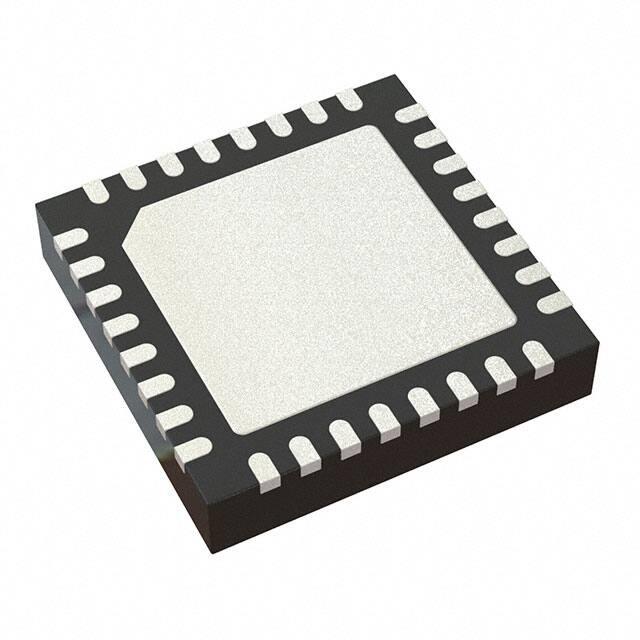


 工商网监
湘ICP备2023018690号
工商网监
湘ICP备2023018690号
