MCP47A1
6-Bit Volatile DAC with Command Code
• 6-Bit DAC
- 65 Taps: 64 Resistors with Taps to Full-Scale
and Zero-Scale (Wiper Code 00h to 40h)
• VREF Pull-down Resistance: 20 k (typical)
• VOUT Voltage Range
- VSS to VREF
• I2C™ Protocol
- Supports SMBus 2.0 Write Byte/Word
Protocol Formats
- Supports SMBus 2.0 Read Byte/Word
Protocol Formats
- Slave Addresses: 5Ch and 7Ch
• Brown-out Reset Protection (1.5V typical)
• Power-on Default Wiper Setting (Mid-scale)
• Low-Power Operation: 90 µA Static Current (typical)
• Wide Operating Voltage Range:
- 1.8V to 5.5V
• Low Tempco: 15 ppm (typical)
• 100 kHz (typical) Bandwidth (-3 dB) Operation
• Extended Temperature Range (-40°C to +125°C)
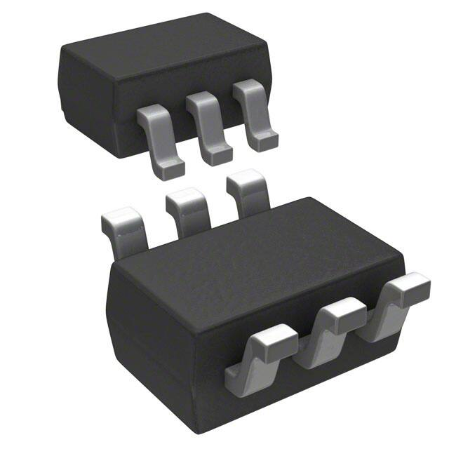
• Small Packages, SC70-6
• Lead Free (Pb-free) Package
Package Types
MCP47A1
VDD 1
A
VSS 2
B
6 VREF
W
5 VOUT
SCL 3
4 SDA
SC70-6
Device Block Diagram
VDD
VSS
SDA
SCL
Power-up
and
Brown-out
Control
2-Wire
Interface
and
Control
Logic
A
Wiper Register (RAB = 20K)
Features:
VREF
VOUT
B
Applications
Description
• Set point or offset trimming
• Cost-sensitive mechanical trim pot replacement
The MCP47A1 devices are volatile, 6-Bit digital
potentiometers with a buffered output. The wiper
setting is controlled through an I2C serial interface. The
I2C slave addresses of “010 1110” and “011 1110”
are supported.
2012 Microchip Technology Inc.
DS25154A-page 1
�MCP47A1
VDD
Operating
Range
65
64
20
00h - 40h
20h
5Ch, 7Ch 1.8V (1)
to 5.5V
VSS to VREF
SC70-6
MCP47DA1(2)
I2C
65
64
30
00h - 7Fh
40h
5Ch, 7Ch 1.8V (1)
to 5.5V
1/3 VREF to
2/3 VREF
SC70-6,
SOT-23-6
MCP4706
I2C 256
256
210
00h - FFh
7Fh
Cxh (3)
2.7V to
5.5V
VSS to VDD or SOT-23-6,
VSS to VREF (5) DFN-6 (2x2)
MCP4716
I2C 1024 1024
210
000h - 3FFh 1FFh
Cxh (3)
2.7V to
5.5V
VSS to VDD or SOT-23-6,
VSS to VREF (5) DFN-6 (2x2)
MCP4726
I2C 4096 4096
210
000h - FFFh 3FFh
Cxh (3)
2.7V to
5.5V
VSS to VDD or SOT-23-6,
VSS to VREF (5) DFN-6 (2x2)
MCP4725
I2C 4096 4096
N.A.
000h - FFFh 3FFh
Cxh (4)
2.7V to
5.5V
VOUT
Range
I2C
I2C Slave
Address
# of
Resistors
POR/BOR
Value
# of Taps
MCP47A1
Device
Data
Value
Range
Interface
VREF
Resistance
(k)
Device Features
VSS to VDD
Package(s)
SOT-23-6
Note 1: Analog characteristics only tested from 2.7V to 5.5V.
2: Refer to MCP47DA1 Data Sheet (DS25118).
3: The A2:A0 bits are determined by device ordered.
4: The A2 and A1 bits are determined by device ordered and A0 is determined by the state of the A0 pin.
5: User programmable.
DS25154A-page 2
2012 Microchip Technology Inc.
�MCP47A1
1.0
ELECTRICAL CHARACTERISTICS
Absolute Maximum Ratings †
Voltage on VDD with respect to VSS .......................................................................................................... 0.6V to +7.0V
Voltage on SCL, and SDA with respect to VSS ..................................................................................................... -0.6V to VDD + 0.3V
Voltage on all other pins (VOUT and VREF) with respect to VSS ..................................................................... -0.3V to VDD + 0.3V
Input clamp current, IIK (VI < 0, VI > VDD) ............................................................................................................ ±20 mA
Output clamp current, IOK (VO < 0 or VO > VDD).................................................................................................. ±20 mA
Maximum output current sunk by any Output pin .................................................................................................. 25 mA
Maximum output current sourced by any Output pin ............................................................................................ 25 mA
Maximum current out of VSS pin .......................................................................................................................... 100 mA
Maximum current into VDD pin ............................................................................................................................. 100 mA
Maximum current into VREF pin............................................................................................................................. 250 uA
Maximum current sourced by VOUT pin ................................................................................................................. 40 mA
Maximum current sunk by VREF pin ....................................................................................................................... 40 mA
Package power dissipation (TA = +50°C, TJ = +150°C)
SC70-6 ..................................................................................................................................................... 480 mW
Storage temperature .............................................................................................................................. -65°C to +150°C
Ambient temperature with power applied .............................................................................................. -40°C to +125°C
ESD protection on all pins .......................................................................................................................... 6 kV (HBM)
..................................................................................................................................................................... 400V (MM)
1.5 kV (CDM)
Latchup (JEDEC JESD78A) at +125°C ............................................................................................................. ±100 mA
Soldering temperature of leads (10 seconds) ...................................................................................................... +300°C
Maximum Junction Temperature (TJ) .................................................................................................................. +150°C
† Notice: Stresses above those listed under “Maximum Ratings” may cause permanent damage to the device. This is
a stress rating only and functional operation of the device at those or any other conditions above those indicated in the
operational listings of this specification is not implied. Exposure to maximum rating conditions for extended periods may
affect device reliability.
2012 Microchip Technology Inc.
DS25154A-page 3
�MCP47A1
AC/DC CHARACTERISTICS
Standard Operating Conditions (unless otherwise specified)
Operating Temperature
–40°C TA +125°C (extended)
DC Characteristics
All parameters apply across the specified operating ranges unless noted.
VDD = +2.7V to +5.5V. CL = 1 nF, RL = 5 k .
Typical specifications represent values for VDD = 5.5V, TA = +25°C.
Parameters
Sym
Min
Typ
Max
Units
Supply Voltage
VDD
2.7
—
5.5
V
Analog Characteristics specified
1.8
—
5.5
V
Digital Characteristics specified
—
—
1.65
V
RAM retention voltage (VRAM) < VBOR
VDD Start Voltage
to ensure Wiper to
default reset state
VBOR
VDD Rise Rate to
ensure Power-on
Reset
VDDRR
Delay after device
exits the reset
state
(VDD > VBOR) to
Digital Interface
Active
TBORD
Delay after device
exits the reset
state
(VDD > VBOR) to
VOUT valid
TOUTV
Supply Current
(Note 6)
VREF Input Range
Note 1:
2:
3:
4:
5:
6:
7:
IDD
VREF
Note 5
—
—
Conditions
V/ms
1
µS
20
µS
Within ± 0.5 LSb of VREF / 2
(for default POR/BOR wiper value).
—
130
220
µA
Serial Interface Active,
Write all 0’s to Volatile Wiper,
No Load on VOUT
VDD = 5.5V, VREF = VDD,
FSCL = 400 kHz
—
90
130
µA
Serial Interface Inactive (Static),
(Stop condition, SCL = SDA = VIH),
No Load on VOUT
Wiper = 0, VDD = 5.5V, VREF = VDD
1
—
VDD
V
Note 7
Resistance is defined as the resistance between the VREF pin and the VSS pin.
INL and DNL are measured at VOUT from Code = 00h (Zero-Scale) through Code = 3Fh (Full-Scale - 1).
This specification by design.
Nonlinearity is affected by wiper resistance (RW), which changes significantly over voltage and
temperature.
POR/BOR is not rate dependent.
Supply current is independent of VREF current.
See Section 7.1.3.
DS25154A-page 4
2012 Microchip Technology Inc.
�MCP47A1
AC/DC CHARACTERISTICS (CONTINUED)
Standard Operating Conditions (unless otherwise specified)
Operating Temperature
–40°C TA +125°C (extended)
DC Characteristics
Parameters
All parameters apply across the specified operating ranges unless noted.
VDD = +2.7V to +5.5V. CL = 1 nF, RL = 5 k .
Typical specifications represent values for VDD = 5.5V, TA = +25°C.
Sym
Min
Typ
Max
Units
Conditions
Minimum Output
Voltage
VOUT(MIN)
—
VSS
—
V
Device Output minimum drive
Maximum Output
Voltage
VOUT(MAX)
—
VREF
—
V
Device Output maximum drive
Output Amplifier
Degree (°) CL = 400 pF, RL =
Phase Margin
PM
—
66
—
Slew Rate
SR
—
0.55
—
V/µs
Short Circuit
Current
ISC
5
15
24
mA
Settling Time
tSETTLING
—
15
—
µs
External Reference (VREF) (Note 3)
CVREF
—
7
—
pF
THD
—
-73
—
dB
Major Code
Transition Glitch
—
45
—
nV-s
Digital
Feedthrough
—
很抱歉,暂时无法提供与“MCP47A1T-A1E/LT”相匹配的价格&库存,您可以联系我们找货
免费人工找货