MCP6441/2/4
450 nA, 9 kHz Op Amp
Features:
Description:
•
•
•
•
•
•
•
•
•
The MCP6441/2/4 device is a single nanopower
operational amplifier (op amp), which has low
quiescent current (450 nA, typical) and rail-to-rail input
and output operation. This op amp is unity gain stable
and has a gain bandwidth product of 9 kHz (typical).
These devices operate with a single supply voltage as
low as 1.4V. These features make the family of op
amps well suited for single-supply, battery-powered
applications.
Low Quiescent Current: 450 nA (typical)
Gain Bandwidth Product: 9 kHz (typical)
Supply Voltage Range: 1.4V to 6.0V
Rail-to-Rail Input and Output
Unity Gain Stable
Slew Rate: 3V/ms (typical)
Extended Temperature Range: -40°C to +125°C
No Phase Reversal
Small Packages
Applications:
•
•
•
•
•
•
Portable Equipment
Battery Powered System
Data Acquisition Equipment
Sensor Conditioning
Battery Current Sensing
Analog Active Filters
The MCP6441/2/4 op amp is designed with Microchip’s
advanced CMOS process and offered in single
(MCP6441), dual (MCP6442), and quad (MCP6444)
configurations. All devices are available in the
extended temperature range, with a power supply
range of 1.4V to 6.0V.
Typical Application
IDD
1.4V
to
6.0V
Design Aids:
•
•
•
•
•
To load
VDD
10Ω
100 kΩ
SPICE Macro Models
FilterLab® Software
Microchip Advanced Part Selector (MAPS)
Analog Demonstration and Evaluation Boards
Application Notes
VOUT
MCP6441
1 MΩ
V DD – VOUT
IDD = -----------------------------------------( 10 V/V ) ⋅ ( 10 Ω )
Battery Current Sensing
Package Types
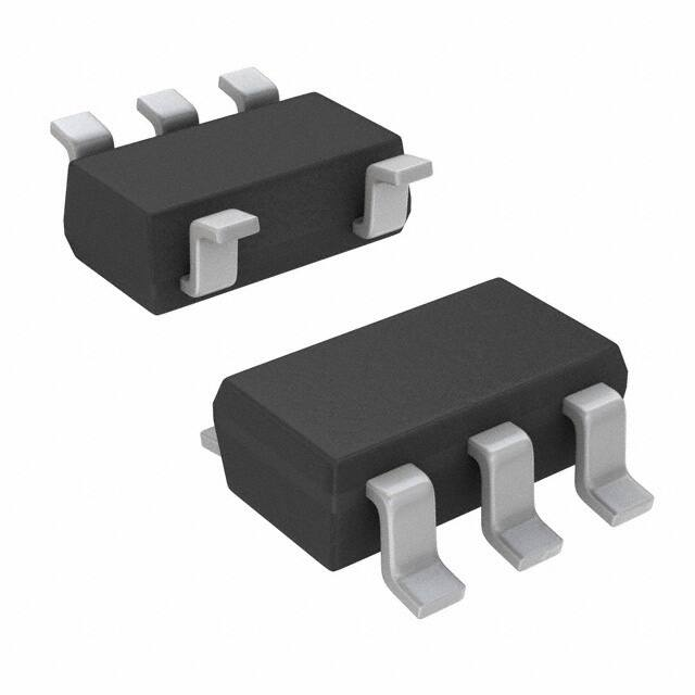
MCP6441
SC70-5, SOT-23-5
VOUT 1
VSS 2
VIN+ 3
5 VDD
4 VIN–
MCP6442
2x3 TDFN *
MCP6442
SOIC, MSOP
VOUTA 1
VINA– 2
VIN+ 3
VSS 4
8
7
6
5
VDD
VOUTB
VOUTA 1
VIN–
VINB+
VIN+ 3
VSS 4
* Includes Exposed Thermal Pad (EP); see Table 3-1.
© 2010-2012 Microchip Technology Inc.
VIN– 2
8 VDD
EP
9
7 VOUTB
6 VINB–
5 VINB+
MCP6444
SOIC, TSSOP
VOUTA
VINA–
VIN+
VDD
VINB+
VINB–
VOUTB
1
2
14 VOUTD
13 VIND–
3
4
12 VIND+
5
10 VINC+
11 VSS
6
9 VINC–
7
8 VOUTC
DS22257C-page 1
�MCP6441/2/4
NOTES:
DS22257C-page 2
© 2010-2012 Microchip Technology Inc.
�MCP6441/2/4
1.0
ELECTRICAL CHARACTERISTICS
1.1
Absolute Maximum Ratings †
Current at Output and Supply Pins ............................±30 mA
† Notice: Stresses above those listed under “Absolute
Maximum Ratings” may cause permanent damage to
the device. This is a stress rating only and functional
operation of the device at those or any other conditions
above those indicated in the operational listings of this
specification is not implied. Exposure to maximum rating conditions for extended periods may affect device
reliability.
Storage Temperature ....................................-65°C to +150°C
†† See Section 4.1.2 “Input Voltage Limits”.
VDD – VSS ........................................................................7.0V
Current at Input Pins .....................................................±2 mA
Analog Inputs (VIN+, VIN-)†† .......... VSS – 1.0V to VDD + 1.0V
All Other Inputs and Outputs ......... VSS – 0.3V to VDD + 0.3V
Difference Input Voltage ...................................... |VDD – VSS|
Output Short-Circuit Current ................................ Continuous
Maximum Junction Temperature (TJ) .......................... +150°C
ESD Protection on All Pins (HBM; MM) ............... ≥ 4 kV; 200V
DC ELECTRICAL SPECIFICATIONS
Electrical Characteristics: Unless otherwise indicated, VDD = +1.4V to +6.0V, VSS= GND, TA= +25°C, VCM = VDD/2,
VOUT ≈ VDD/2, VL = VDD/2 and RL = 1 MΩ to VL. (Refer to Figure 1-1).
Parameters
Sym
Min
Typ
Max
Units
VOS
-4.5
—
+4.5
mV
ΔVOS/ΔTA
—
±2.5
—
PSRR
65
86
—
dB
IB
—
±1
—
pA
Conditions
Input Offset
Input Offset Voltage
Input Offset Drift with Temperature
Power Supply Rejection Ratio
VCM = VSS
µV/°C TA= -40°C to +125°C,
VCM = VSS
VCM = VSS
Input Bias Current and Impedance
Input Bias Current
—
20
—
pA
TA = +85°C
—
400
—
pA
TA = +125°C
—
±1
—
pA
—
1013||6
—
Ω||pF
ZDIFF
—
1013||6
—
Ω||pF
Common Mode Input Voltage Range
VCMR
VSS-0.3
—
VDD+0.3
V
Common Mode Rejection Ratio
CMRR
60
76
—
dB
VCM = -0.3V to 6.3V,
VDD = 6.0V
AOL
90
110
—
dB
VOUT = 0.1V to VDD-0.1V
RL = 10 kΩ to VL
VOL, VOH
VSS+20
—
VDD–20
mV
VDD = 6.0V, RL = 10 kΩ
0.5V input overdrive
Input Offset Current
Common Mode Input Impedance
Differential Input Impedance
IOS
ZCM
Common Mode
Open-Loop Gain
DC Open-Loop Gain
(Large Signal)
Output
Maximum Output Voltage Swing
Output Short-Circuit Current
ISC
—
±3
—
mA
VDD = 1.4V
—
±22
—
mA
VDD = 6.0V
VDD
1.4
—
6.0
V
IQ
250
450
650
nA
Power Supply
Supply Voltage
Quiescent Current per Amplifier
© 2010-2012 Microchip Technology Inc.
IO = 0, VDD = 5.0V
DS22257C-page 3
�MCP6441/2/4
AC ELECTRICAL SPECIFICATIONS
Electrical Characteristics: Unless otherwise indicated, TA = +25°C, VDD = +1.4V to +6.0V, VSS = GND,
VCM = VDD/2, VOUT ≈ VDD/2, VL = VDD/2, RL = 1 MΩ to VL and CL = 60 pF. (Refer to Figure 1-1).
Parameters
Sym
Min
Typ
Max
Units
kHz
Conditions
AC Response
Gain Bandwidth Product
GBWP
—
9
—
Phase Margin
PM
—
65
—
°
Slew Rate
SR
—
3
—
V/ms
Input Noise Voltage
Eni
—
5
—
µVp-p
f = 0.1 Hz to 10 Hz
Input Noise Voltage Density
eni
—
190
—
nV/√Hz
f = 1 kHz
Input Noise Current Density
ini
—
0.6
—
fA/√Hz
f = 1 kHz
G = +1 V/V
Noise
TEMPERATURE SPECIFICATIONS
Electrical Characteristics: Unless otherwise indicated, VDD = +1.4V to +6.0V and VSS = GND.
Parameters
Sym
Min
Typ
Max
Units
Operating Temperature Range
TA
-40
—
+125
°C
Storage Temperature Range
TA
-65
—
+150
°C
Conditions
Temperature Ranges
Note 1
Thermal Package Resistances
Thermal Resistance, 5L-SC70
θJA
—
331
—
°C/W
Thermal Resistance, 5L-SOT-23
θJA
—
220.7
—
°C/W
Thermal Resistance, 8L-MSOP
θJA
—
211
—
°C/W
Thermal Resistance, 8L-SOIC
θJA
—
149.5
—
°C/W
Thermal Resistance, 8L-2x3 TDFN
θJA
—
52.5
—
°C/W
Thermal Resistance, 14L-SOIC
θJA
—
95.3
—
°C/W
Thermal Resistance, 14L-TSSOP
θJA
—
100
—
°C/W
Note 1:
1.2
The internal junction temperature (TJ) must not exceed the absolute maximum specification of +150°C.
Test Circuits
The circuit used for most DC and AC tests is shown in
Figure 1-1. This circuit can independently set VCM and
VOUT (see Equation 1-1). Note that VCM is not the
circuit’s Common Mode voltage ((VP + VM)/2), and that
VOST includes VOS plus the effects (on the input offset
error, VOST) of the temperature, CMRR, PSRR and
AOL.
EQUATION 1-1:
G DM = RF ⁄ RG
CF
6.8 pF
RG
100 kΩ
VP
VDD
VIN+
CB1
100 nF
MCP6441
V CM = ( V P + V DD ⁄ 2 ) ⁄ 2
VDD/2
CB2
1 µF
VIN–
V OST = VIN– – VIN+
V OUT = ( V DD ⁄ 2 ) + ( V P – V M ) + VOST ( 1 + G DM )
Where:
GDM = Differential Mode Gain
(V/V)
VCM = Op Amp’s Common Mode
Input Voltage
(V)
VOST = Op Amp’s Total Input Offset Voltage (mV)
DS22257C-page 4
RF
100 kΩ
VM
RG
100 kΩ
RL
1 MΩ
RF
100 kΩ
CF
6.8 pF
VOUT
CL
60 pF
VL
FIGURE 1-1:
AC and DC Test Circuit for
Most Specifications.
© 2010-2012 Microchip Technology Inc.
�MCP6441/2/4
2.0
TYPICAL PERFORMANCE CURVES
Note:
The graphs and tables provided following this note are a statistical summary based on a limited number of
samples and are provided for informational purposes only. The performance characteristics listed herein
are not tested or guaranteed. In some graphs or tables, the data presented may be outside the specified
operating range (e.g., outside specified power supply range) and therefore outside the warranted range.
Note: Unless otherwise indicated, TA = +25°C, VDD = +1.4V to +6.0V, VSS = GND, VCM = VDD/2, VOUT ≈ VDD/2,
VL = VDD/2, RL = 1 MΩ to VL and CL = 60 pF.
4000
Input Offset Voltage (µV)
FIGURE 2-3:
Input Offset Voltage vs.
Common Mode Input Voltage with VDD = 6.0V.
© 2010-2012 Microchip Technology Inc.
1.7
1.5
1.3
6.0
5.5
4.5
4.0
5.0
6.5
6.0
5.5
6.5
6.0
5.5
5.0
4.5
4.0
3.5
3.0
2.5
2.0
1.5
1.0
0.5
0.0
-0.5
Common Mode Input Voltage (V)
Representative Part
5.0
0
-500
+125°C
+85°C
+25°C
-40°C
4.5
500
TA =
TA =
TA =
TA =
4.0
1000
1.0
TA = +125°C
TA = +85°C
TA = +25°C
TA = -40°C
2000
1600
1200
800
400
0
-400
-800
-1200
-1600
-2000
3.0
VDD = 6.0V
Representative Part
Input Offset Voltage (µV)
Input Offset Voltage (µV)
3000
Input Offset Voltage vs.
3.5
FIGURE 2-5:
Output Voltage.
2.5
Input Offset Voltage Drift.
1500
3.5
Output Voltage (V)
Input Offset Voltage Drift (µV/°C)
2000
3.0
0.0
10
8
6
4
2
0
-2
-4
-6
-10
-8
0%
Representative Part
2.5
5%
2.0
10%
VDD = 6.0V
1.5
15%
VDD = 1.4V
1.0
20%
1000
800
600
400
200
0
-200
-400
-600
-800
-1000
0.5
Input Offset Voltage (µV)
Percentage of Occurences
1700 Samples
VCM = VSS
TA = -40°C to +125°C
2500
1.1
FIGURE 2-4:
Input Offset Voltage vs.
Common Mode Input Voltage with VDD = 1.4V.
30%
FIGURE 2-2:
0.9
Common mode input voltage (V)
Input Offset Voltage.
25%
0
-0.3
Input Offset Voltage (mV)
FIGURE 2-1:
500
-500
4.5
3.5
2.5
1.5
0.5
-0.5
-1.5
-2.5
-3.5
0%
1000
0.7
5%
1500
0.5
10%
2000
0.3
15%
2500
0.1
20%
VDD = 1.4V
Representative Part
TA = +125°C
TA = +85°C
TA = +25°C
TA = -40°C
3000
2.0
25%
3500
-0.1
1700 Samples
VCM = VSS
1.5
30%
-4.5
Percentage of Occurences
35%
Power Supply Voltage (V)
FIGURE 2-6:
Input Offset Voltage vs.
Power Supply Voltage.
DS22257C-page 5
�MCP6441/2/4
Note: Unless otherwise indicated, TA = +25°C, VDD = +1.4V to +6.0V, VSS = GND, VCM = VDD/2, VOUT ≈ VDD/2,
VL = VDD/2, RL = 1 MΩ to VL and CL = 60 pF.
CMRR,PSRR (dB)
Input Noise Voltage Density
(nV/�Hz)
1,000
100
0.1
0.1
11
10
100
10
100
Frequency (Hz)
10k
10000
Input Noise Voltage Density
PSRR (VDD = 1.4V to 6.0V, VCM = VSS)
CMRR (VDD = 6.0V, VCM = -0.3V to 6.3V)
CMRR (VDD = 1.4V, VCM = -0.3V to 1.7V)
-50
-25
100
125
CMRR, PSRR vs. Ambient
1000
350
300
250
VDD = 6.0V
100
200
150
100
f = 1 kHz
VDD = 6.0 V
50
Input Bias Current
10
Input Offset Current
1
6.5
6.0
5.5
5.0
4.5
4.0
3.5
3.0
2.5
2.0
1.5
1.0
0.5
0.0
-0.5
0
25
45
65
85
105
Ambient Temperature (°C)
Common Mode Input Voltage (V)
FIGURE 2-8:
Input Noise Voltage Density
vs. Common Mode Input Voltage.
100
125
FIGURE 2-11:
Input Bias, Offset Current
vs. Ambient Temperature.
1000
Input Bias Current (pA)
Representative Part
PSRR-
90
80
PSRR+
70
CMRR
60
c
50
40
30
TA = +125°C
100
TA = +85°C
10
VDD = 6.0V
FIGURE 2-9:
Frequency.
DS22257C-page 6
CMRR, PSRR vs.
6.0
5.5
5.0
4.5
4.0
3.5
3.0
1000
2.5
100
2.0
10
Frequency (Hz)
1.5
1
1.0
0.1
0.5
1
20
0.0
CMRR, PSRR (dB)
0
25
50
75
Ambient Temperature (°C)
FIGURE 2-10:
Temperature.
Input Bias and Offset Currents
(pA)
Input Noise Voltage Density
(nV/�Hz)
FIGURE 2-7:
vs. Frequency.
1k
1000
100
95
90
85
80
75
70
65
60
55
50
Common Mode Input Voltage (V)
FIGURE 2-12:
Input Bias Current vs.
Common Mode Input Voltage.
© 2010-2012 Microchip Technology Inc.
�MCP6441/2/4
Note: Unless otherwise indicated, TA = +25°C, VDD = +1.4V to +6.0V, VSS = GND, VCM = VDD/2, VOUT ≈ VDD/2,
VL = VDD/2, RL = 1 MΩ to VL and CL = 60 pF.
130
DC Open-Loop Gain (dB)
600
VDD = 6.0V
500
450
400
350
VDD = 1.4V
300
250
110
100
90
80
RL = 10 kΩ
VSS + 0.1V < VOUT < VDD - 0.1V
70
FIGURE 2-13:
Quiescent Current vs.
Ambient Temperature.
6.0
5.5
5.0
4.5
4.0
3.5
125
3.0
0
25
50
75
100
Ambient Temperature (°C)
2.5
-25
1.0
-50
2.0
60
200
Power Supply Voltage (V)
FIGURE 2-16:
DC Open-Loop Gain vs.
Power Supply Voltage.
700
130
DC O
Open-Lo
oop Ga
ain (dB
B)
600
Quiescent Current
(nA/Amplifier)
120
1.5
Quiescent Current
(nA/Amplifier)
550
500
400
300
TA =
TA =
TA =
TA =
200
100
+125°C
+85°C
+25°C
-40°C
7.0
6.5
6.0
5.5
4.5
5.0
4.0
3.5
3.0
2.5
2.0
1.5
1.0
0.5
0.0
0
VDD = 6.0V
120
110
100
VDD = 1.4V
90
80
L
Large
Signal
Si
l AOL
70
RL = 10k:
60
0.00
0.05
0.10
0.15
0.20
0.25
Power Supply Voltage (V)
100
80
18
-30
16
-60
Open-Loop Phase
60
40
-90
-120
20
0
0
-150
-180
VDD = 6.0V
-20
-210
1.0E-03 1.0E-02 1.0E-01 1.0E+00 1.0E+01 1.0E+02 1.0E+03 1.0E+04 1.0E+05
1m 10m 0.1 1 10 100 1k 10k 100k
Frequency (Hz)
FIGURE 2-15:
Frequency.
Open-Loop Gain, Phase vs.
© 2010-2012 Microchip Technology Inc.
Gain Bandwidth Product
(kHz)
Open-Loop Gain
Open-Loop Phase (°)
Open-Loop Gain (dB)
120
FIGURE 2-17:
DC Open-Loop Gain vs.
Output Voltage Headroom.
90
Phase Margin
80
14
70
12
60
10
50
8
40
Gain Bandwidth Product
6
30
4
20
VDD = 6.0V
2
10
0
-50
Phase Margin (°)
FIGURE 2-14:
Quiescent Current vs.
Power Supply Voltage.
-25
0
25
50
75 100
Ambient Temperature (°C)
0
125
FIGURE 2-18:
Gain Bandwidth Product,
Phase Margin vs. Ambient Temperature.
DS22257C-page 7
�MCP6441/2/4
90
Phase Margin
16
80
14
70
12
60
10
50
Gain Bandwidth Product
8
40
6
30
4
20
VDD = 1.4V
2
10
0
-50
-25
Phase Margin (°)
Gain Bandwidth Product
(kHz)
18
0
25
50
75 100
Ambient Temperature (°C)
0
125
1000
10
RL = 10 kΩ
0.1
0.01
10
0.1
1
100
1000
Output Current (mA)
10
10000
FIGURE 2-22:
Output Voltage Headroom
vs. Output Current.
Output Voltage Headroom
VDD - VOH or VOL - VSS (mV)
TA = -40°C
TA = +25°C
TA = +85°C
TA = +125°C
25
20
15
10
5
15
10
5
FIGURE 2-20:
Output Short Circuit Current
vs. Power Supply Voltage.
VDD - VOH @ VDD = 1.4V
VOL - VSS @ VDD = 1.4V
0
6.0
5.5
5.0
4.5
4.0
3.5
3.0
2.5
2.0
1.5
1.0
0.5
0
VDD - VOH @ VDD = 6.0V
VOL - VSS @ VDD = 6.0V
20
-50
Power Supply Voltage (V)
-25
0
25
50
75
100
Ambient Temperature (°C)
125
FIGURE 2-23:
Output Voltage Headroom
vs. Ambient Temperature.
6
VDD = 6.0V
Falling Edge, VDD = 6.0V
Rising Edge, VDD = 6.0V
5
Slew Rate (V/ms)
Output Voltage Swing (V P-P)
VDD - VOH @ VDD = 6.0V
VOL - VSS @ VDD = 6.0V
1
25
30
10
VDD - VOH @ VDD = 1.4V
VOL - VSS @ VDD = 1.4V
100
35
0.0
Output Short Circuit Current
(mA)
FIGURE 2-19:
Gain Bandwidth Product,
Phase Margin vs. Ambient Temperature.
Output Voltage Headroom (mV)
Note: Unless otherwise indicated, TA = +25°C, VDD = +1.4V to +6.0V, VSS = GND, VCM = VDD/2, VOUT ≈ VDD/2,
VL = VDD/2, RL = 1 MΩ to VL and CL = 60 pF.
VDD = 1.4V
1
4
3
2
Falling Edge, VDD = 1.4V
Rising Edge, VDD = 1.4V
1
0
0.1
10
FIGURE 2-21:
Frequency.
DS22257C-page 8
100
1k
100
1000
Frequency (Hz)
10k
10000
Output Voltage Swing vs.
-50
-25
FIGURE 2-24:
Temperature.
0
25
50
75
Ambient Temperature (°C)
100
125
Slew Rate vs. Ambient
© 2010-2012 Microchip Technology Inc.
�MCP6441/2/4
VDD = 6.0V
G = +1 V/V
6.0
5.5
5.0
4.5
4.0
3.5
3.0
2.5
2.0
1.5
1.0
0.5
0.0
Output Voltage (V)
Output Voltage (20 mv/div)
Note: Unless otherwise indicated, TA = +25°C, VDD = +1.4V to +6.0V, VSS = GND, VCM = VDD/2, VOUT ≈ VDD/2,
VL = VDD/2, RL = 1 MΩ to VL and CL = 60 pF.
Time (200 µs/div)
FIGURE 2-25:
Pulse Response.
Small Signal Non-Inverting
VDD = 6.0V
G = -1 V/V
Time (2 ms/div)
FIGURE 2-28:
Response.
Large Signal Inverting Pulse
VDD = 6.0V
G = -1 V/V
Input,Output Voltage (V)
Output Voltage (20 mv/div)
7.0
6.0
5.0
VOUT
VIN
4.0
3.0
2.0
1.0
VDD = 6.0V
G = +2 V/V
0.0
-1.0
Time (2 ms/div)
Time (200 µs/div)
6.0
5.5
5.0
4.5
4.0
3.5
3.0
2.5
2.0
1.5
1.0
0.5
0.0
Small Signal Inverting Pulse
1M
1000000
VDD = 6.0V
G = +1 V/V
Time (2 ms/div)
FIGURE 2-27:
Pulse Response.
FIGURE 2-29:
The MCP6441/2/4 Device
Shows No Phase Reversal.
Large Signal Non-Inverting
© 2010-2012 Microchip Technology Inc.
Closed Loop Output
Impedance (Ω)
Output Voltage (V)
FIGURE 2-26:
Response.
100k
100000
10k
10000
1k
1000
G N:
101 V/V
11 V/V
1 V/V
100
100
10
10
1
1
1
1
10
10
100
100
1000
1k
10000
10k
Frequency (Hz)
FIGURE 2-30:
Closed Loop Output
Impedance vs. Frequency.
DS22257C-page 9
�MCP6441/2/4
100µ
1.E-04
-IIN (A)
10µ
1.E-05
1µ
1.E-06
100n
1.E-07
10n
1.E-08
1n
1.E-09
100p
1.E-10
10p
1.E-11
TA = -40°C
TA = +25°C
TA = +85°C
TA = +125°C
1p
1.E-12
-1.0 -0.9 -0.8 -0.7 -0.6 -0.5 -0.4 -0.3 -0.2 -0.1 0.0
Input Voltage (V)
FIGURE 2-31:
Measured Input Current vs.
Input Voltage (below VSS).
DS22257C-page 10
n 150
o
ti
140
a
r
a 130
p
e
S 120
l
e ) 110
n
n B
a (d 100
h
C
90
to
l
80
e
n
n
70
a
h
60
C
(dB)
1m
1.E-03
Channel to Channel Separation
Note: Unless otherwise indicated, TA = +25°C, VDD = +1.4V to +6.0V, VSS = GND, VCM = VDD/2, VOUT ≈ VDD/2,
VL = VDD/2, RL = 1 MΩ to VL and CL = 60 pF.
Input Referred
100
100
100
1k
1000
1k
Frequency (Hz)
10k
10000
FIGURE 2-32:
Channel-to-Channel
Separation vs. Frequency (MCP6442/4 only).
© 2010-2012 Microchip Technology Inc.
�MCP6441/2/4
3.0
PIN DESCRIPTIONS
Descriptions of the pins are listed in Table 3-1.
TABLE 3-1:
PIN FUNCTION TABLE
MCP6441
MCP6442
MCP6444
SC70-5,
SOT-23-5
SOIC,
MSOP
2x3 TDFN
SOIC,
TSSOP
1
1
1
1
3.1
Description
VOUT, VOUTA Analog Output (op amp A)
4
2
2
2
VIN–, VINA–
Inverting Input (op amp A)
3
3
3
3
VIN+, VINA+
Non-inverting Input (op amp A)
5
8
8
4
VDD
—
5
5
5
VINB+
—
6
6
6
VINB-
Inverting Input (op amp B)
—
7
7
7
VOUTB
Analog Output (op amp B)
—
—
—
8
VOUTC
Analog Output (op amp C)
—
—
—
9
VINC-
Inverting Input (op amp C)
—
—
—
10
VINC+
Non-inverting Input (op amp C)
2
4
4
11
VSS
Positive Power Supply
Non-inverting Input (op amp B)
Negative Power Supply
—
—
—
12
VIND+
Non-inverting Input (op amp D)
—
—
—
13
VIND-
Inverting Input (op amp D)
—
—
—
14
VOUTD
Analog Output (op amp D)
—
—
9
—
EP
Analog Output (VOUT)
The output pin is a low-impedance voltage source.
3.2
Symbol
Power Supply Pins (VDD, VSS)
The positive power supply (VDD) is 1.4V to 6.0V higher
than the negative power supply (VSS). For normal
operation, the other pins are at voltages between VSS
and VDD.
Typically, these parts are used in a single (positive)
supply configuration. In this case, VSS is connected to
ground and VDD is connected to the supply. VDD will
need bypass capacitors.
© 2010-2012 Microchip Technology Inc.
3.3
Exposed Thermal Pad (EP);
must be connected to VSS
Analog Inputs (VIN+, VIN-)
The non-inverting and inverting inputs are highimpedance CMOS inputs with low bias currents.
3.4
Exposed Thermal Pad (EP)
There is an internal connection between the Exposed
Thermal Pad (EP) and the VSS pin; they must be connected to the same potential on the Printed Circuit
Board (PCB).
This pad can be connected to a PCB ground plane to
provide a larger heat sink. This improves the package
thermal resistance (θJA).
DS22257C-page 11
�MCP6441/2/4
Notes:
DS22257C-page 12
© 2010-2012 Microchip Technology Inc.
�MCP6441/2/4
4.0
APPLICATION INFORMATION
The MCP6441/2/4 op amp is manufactured using
Microchip’s state-of-the-art CMOS process, specifically
designed for low power applications.
4.1
In some applications, it may be necessary to prevent
excessive voltages from reaching the op amp inputs;
Figure 4-2 shows one approach to protecting these
inputs.
VDD
Rail-to-Rail Input
4.1.1
PHASE REVERSAL
The MCP6441/2/4 op amp is designed to prevent
phase reversal, when the input pins exceed the supply
voltages. Figure 2-29 shows the input voltage
exceeding the supply voltage with no phase reversal.
4.1.2
D1
D2
V1
MCP644X
VOUT
V2
INPUT VOLTAGE LIMITS
In order to prevent damage and/or improper operation
of the amplifier, the circuit must limit the voltages at the
input pins (see Section 1.1, Absolute Maximum
Ratings †).
The Electrostatic Discharge (ESD) protection on the
inputs can be depicted as shown in Figure 4-1. This
structure was chosen to protect the input transistors
against many, but not all, over-voltage conditions, and
to minimize the input bias current (IB).
VDD
Bond
Pad
VIN+ Bond
Pad
Input
Stage
Bond V –
IN
Pad
FIGURE 4-2:
Inputs.
Protecting the Analog
A significant amount of current can flow out of the
inputs when the Common Mode voltage (VCM) is below
ground (VSS); see Figure 2-31.
4.1.3
INPUT CURRENT LIMITS
In order to prevent damage and/or improper operation
of the amplifier, the circuit must limit the currents into
the input pins (see Section 1.1 “Absolute Maximum
Ratings †”).
Figure 4-3 shows one approach to protecting these
inputs. The resistors R1 and R2 limit the possible
currents in or out of the input pins (and the ESD diodes,
D1 and D2). The diode currents will go through either
VDD or VSS.
VDD
VSS Bond
Pad
FIGURE 4-1:
Structures.
D1
Simplified Analog Input ESD
The input ESD diodes clamp the inputs when they try
to go more than one diode drop below VSS. They also
clamp any voltages that go well above VDD; their
breakdown voltage is high enough to allow normal
operation, but not low enough to protect against slow
over-voltage (beyond VDD) events. Very fast ESD
events that meet the spec are limited so that damage
does not occur.
© 2010-2012 Microchip Technology Inc.
D2
V1
VOUT
R1
MCP644X
V2
R2
min(R1,R2) >
VSS – min(V1, V2)
2 mA
min(R1,R2) >
max(V1,V2) – VDD
2 mA
FIGURE 4-3:
Inputs.
Protecting the Analog
DS22257C-page 13
�MCP6441/2/4
NORMAL OPERATION
The input stage of the MCP6441/2/4 op amp uses two
differential input stages in parallel. One operates at a
low Common Mode input voltage (VCM), while the other
operates at a high VCM. With this topology, the device
operates with a VCM up to 300 mV above VDD and
300 mV below VSS. The input offset voltage is
measured at VCM = VSS – 0.3V and VDD + 0.3V, to
ensure proper operation.
Figure 4-5 gives the recommended RISO values for the
different capacitive loads and gains. The x-axis is the
normalized load capacitance (CL/GN), where GN is the
circuit's noise gain. For non-inverting gains, GN and the
Signal Gain are equal. For inverting gains, GN is
1+|Signal Gain| (e.g., -1 V/V gives GN = +2 V/V).
1000000
1M
Recommended RISO (Ω)
4.1.4
The transition between the input stages occurs when
VCM is near VDD – 0.6V (see Figures 2-3 and 2-4). For
the best distortion performance and gain linearity, with
non-inverting gains, avoid this region of operation.
4.2
Rail-to-Rail Output
The output voltage range of the MCP6441/2/4 op amp
is VSS + 20 mV (minimum) and VDD – 20 mV (maximum) when RL = 10 kΩ is connected to VDD/2 and
VDD = 6.0V. Refer to Figures 2-22 and 2-23 for more
information.
4.3
Capacitive Loads
Driving large capacitive loads can cause stability
problems for voltage feedback op amps. As the load
capacitance increases, the feedback loop’s phase
margin decreases, and the closed-loop bandwidth is
reduced. This produces gain peaking in the frequency
response, with overshoot and ringing in the step
response. While a unity-gain buffer (G = +1 V/V) is the
most sensitive to the capacitive loads, all gains show
the same general behavior.
When driving large capacitive loads with the
MCP6441/2/4 op amp (e.g., > 100 pF when
G = +1 V/V), a small series resistor at the output (RISO
in Figure 4-4) improves the feedback loop’s phase margin (stability) by making the output load resistive at
higher frequencies. The bandwidth will be generally
lower than the bandwidth with no capacitance load.
–
VIN
MCP644X
+
RISO
VOUT
CL
100k
100000
10k
10000
G N:
1 V/V
2 V/V
≥ 5 V/V
1k
1000
10p 1.E-10
100p 1.E-09
1n
10n
0.1µ
1µ
1.E-11
1.E-08
1.E-07
1.E-06
Normalized Load Capacitance; CL/GN (F)
FIGURE 4-5:
Recommended RISO Values
for Capacitive Loads.
After selecting RISO for your circuit, double-check the
resulting frequency response peaking and step
response overshoot. Modify RISO’s value until the
response is reasonable. Bench evaluation and
simulations with the MCP6441/2/4 SPICE macro
model are very helpful.
4.4
Supply Bypass
The MCP6441/2/4 op amp’s power supply pin (VDD for
single-supply) should have a local bypass capacitor
(i.e., 0.01 µF to 0.1 µF) within 2 mm for good high
frequency performance. It can use a bulk capacitor
(i.e., 1 µF or larger) within 100 mm to provide large,
slow currents. This bulk capacitor can be shared with
other analog parts.
4.5
PCB Surface Leakage
In applications where low input bias current is critical,
Printed Circuit Board (PCB) surface leakage effects
need to be considered. Surface leakage is caused by
humidity, dust or other contamination on the board.
Under low humidity conditions, a typical resistance
between nearby traces is 1012Ω. A 5V difference would
cause 5 pA of current to flow, which is greater than the
MCP6441/2/4 op amp’s bias current at +25°C (±1 pA,
typical).
FIGURE 4-4:
Output Resistor, RISO
Stabilizes Large Capacitive Loads.
DS22257C-page 14
© 2010-2012 Microchip Technology Inc.
�MCP6441/2/4
The easiest way to reduce surface leakage is to use a
guard ring around sensitive pins (or traces). The guard
ring is biased at the same voltage as the sensitive pin.
An example of this type of layout is shown in
Figure 4-6.
Guard Ring
FIGURE 4-6:
for Inverting Gain.
1.
2.
VIN– VIN+
VSS
Example Guard Ring Layout
Non-inverting Gain and Unity-Gain Buffer:
a) Connect the non-inverting pin (VIN+) to the
input with a wire that does not touch the
PCB surface.
b) Connect the guard ring to the inverting input
pin (VIN–). This biases the guard ring to the
Common Mode input voltage.
Inverting Gain and Transimpedance Gain
Amplifiers (convert current to voltage, such as
photo detectors):
a) Connect the guard ring to the non-inverting
input pin (VIN+). This biases the guard ring
to the same reference voltage as the op
amp (e.g., VDD/2 or ground).
b) Connect the inverting pin (VIN–) to the input
with a wire that does not touch the PCB
surface.
© 2010-2012 Microchip Technology Inc.
4.6
4.6.1
Application Circuits
BATTERY CURRENT SENSING
The MCP6441/2/4 op amp’s Common Mode Input
Range, which goes 0.3V beyond both supply rails,
supports their use in high-side and low-side battery
current sensing applications. The low quiescent current
(450 nA, typical) helps prolong battery life, and the
rail-to-rail output supports detection of low currents.
Figure 4-7 shows a high side battery current sensor
circuit. The 10Ω resistor is sized to minimize power
losses. The battery current (IDD) through the 10Ω
resistor causes its top terminal to be more negative
than the bottom terminal. This keeps the Common
Mode input voltage of the op amp below VDD, which is
within its allowed range. The output of the op amp will
also be below VDD, within its Maximum Output Voltage
Swing specification.
IDD
1.4V
to
6.0V
To load
10Ω
100 kΩ
VDD
VOUT
MCP6441
1 MΩ
VDD – VOUT
I DD = -----------------------------------------( 10 V/V ) ⋅ ( 10 Ω )
FIGURE 4-7:
Battery Current Sensing.
DS22257C-page 15
�MCP6441/2/4
4.6.2
PRECISION HALF-WAVE
RECTIFIER
4.6.3
The precision half-wave rectifier, which is also known
as a super diode, is a configuration obtained with an
operational amplifier in order to have a circuit behaving
like an ideal diode and rectifier. It effectively cancels the
forward voltage drop of the diode in such a way that
very low level signals can still be rectified, with minimal
error. This can be useful for high-precision signal
processing. The MCP6441/2/4 op amp has high input
impedance, low input bias current and rail-to-rail
input/output, which makes this device suitable for
precision rectifier applications.
Figure 4-8 shows a precision half-wave rectifier and its
transfer characteristic. The rectifier’s input impedance
is determined by the input resistor R1. To avoid the
loading effect, it must be driven from a low-impedance
source.
When VIN is greater than zero, D1 is OFF, D2 is ON, and
VOUT is zero. When VIN is less than zero, D1 is ON, D2
is OFF, and VOUT is the VIN with an amplification of
-R2/R1.
The rectifier circuit shown in Figure 4-8 has the benefit
that the op amp never goes in saturation, so the only
thing affecting its frequency response is the
amplification and the gain bandwidth product.
INSTRUMENTATION AMPLIFIER
The MCP6441/2/4 op amp is well suited for conditioning sensor signals in battery-powered applications.
Figure 4-9 shows a two op amp instrumentation
amplifier, using the MCP6441/2/4 device, that works
well for applications requiring rejection of Common
Mode noise at higher gains. The reference voltage
(VREF) is supplied by a low-impedance source. In single supply applications, VREF is typically VDD/2.
RG
VREF R1
R2
R2
R1
VOUT
V2
1/2 MCP6442
1/2 MCP6442
V1
R1 2R 1
VOUT = ( V1 – V 2 ) ⎛⎝ 1 + ------ + ---------⎞⎠ + VREF
R2 RG
FIGURE 4-9:
Two Op Amp
Instrumentation Amplifier.
.
R2
D2
VIN
R1
VOUT
MCP6441
D1
Precision Half-Wave Rectifier
VOUT
-R2/R1
VIN
Transfer Characteristic
FIGURE 4-8:
Rectifier.
DS22257C-page 16
Precision Half-Wave
© 2010-2012 Microchip Technology Inc.
�MCP6441/2/4
5.0
DESIGN AIDS
Microchip provides the basic design tools needed for
the MCP6441/2/4 op amp.
5.1
SPICE Macro Model
The latest SPICE macro model for the MCP6441/2/4
op amp is available on the Microchip web site at
www.microchip.com. The model was written and tested
in the official OrCAD (Cadence®) owned PSpice®. For
the other simulators, translation may be required.
5.4
Analog Demonstration and
Evaluation Boards
Microchip offers a broad spectrum of Analog
Demonstration and Evaluation Boards that are
designed to help you achieve faster time to market. For
a complete listing of these boards and their
corresponding user’s guides and technical information,
visit
the
Microchip
web
site
at
www.microchip.com/analogtools.
Some boards that are especially useful are:
The model covers a wide aspect of the op amp's
electrical specifications. Not only does the model cover
voltage, current and resistance of the op amp, but it
also covers the temperature and the noise effects on
the behavior of the op amp. The model has not been
verified outside of the specification range listed in the
op amp data sheet. The model behaviors under these
conditions cannot ensure it will match the actual op
amp performance.
•
•
•
•
•
•
Moreover, the model is intended to be an initial design
tool. Bench testing is a very important part of any
design and cannot be replaced with simulations. Also,
simulation results using this macro model need to be
validated by comparing them to the data sheet
specifications and characteristic curves.
The following Microchip Analog Design Note and
Application Notes are available on the Microchip web
site at www.microchip.com/appnotes, and are
recommended as supplemental reference resources.
5.2
FilterLab® Software
Microchip’s FilterLab software is an innovative software
tool that simplifies analog active filter design using op
amps. Available at no cost from the Microchip web site
at www.microchip.com/filterlab, the FilterLab design
tool provides full schematic diagrams of the filter circuit
with component values. It also outputs the filter circuit
in SPICE format, which can be used with the macro
model to simulate the actual filter performance.
5.3
Microchip Advanced Part Selector
(MAPS)
MAPS is a software tool that helps semiconductor
professionals efficiently identify the Microchip devices
that fit a particular design requirement. Available at no
cost
from
the
Microchip
website
at
www.microchip.com/ maps, the MAPS is an overall
selection tool for Microchip’s product portfolio that
includes Analog, Memory, MCUs and DSCs. Using this
tool, you can define a filter to sort features for a
parametric search of devices and export side-by-side
technical comparison reports. Helpful links are also
provided for Data Sheets, Purchase and Sampling of
Microchip parts.
© 2010-2012 Microchip Technology Inc.
MCP6XXX Amplifier Evaluation Board 1
MCP6XXX Amplifier Evaluation Board 2
MCP6XXX Amplifier Evaluation Board 3
MCP6XXX Amplifier Evaluation Board 4
Active Filter Demo Board Kit
5/6-Pin SOT-23 Evaluation Board, P/N VSUPEV2
5.5
Application Notes
• ADN003 – “Select the Right Operational Amplifier
for your Filtering Circuits”, DS21821
• AN722 – “Operational Amplifier Topologies and
DC Specifications”, DS00722
• AN723 – “Operational Amplifier AC Specifications
and Applications”, DS00723
• AN884 – “Driving Capacitive Loads With Op
Amps”, DS00884
• AN990 – “Analog Sensor Conditioning Circuits –
An Overview”, DS00990
• AN1177 – “Op Amp Precision Design: DC Errors”,
DS01177
• AN1228 – “Op Amp Precision Design: Random
Noise”, DS01228
• AN1297 – “Microchip’s Op Amp SPICE Macro
Models”, DS01297
• AN1332: “Current Sensing Circuit Concepts and
Fundamentals”’ DS01332
These application notes and others are listed in the
design guide:
• “Signal Chain Design Guide”, DS21825
DS22257C-page 17
�MCP6441/2/4
NOTES:
DS22257C-page 18
© 2010-2012 Microchip Technology Inc.
�MCP6441/2/4
6.0
PACKAGING INFORMATION
6.1
Package Marking Information
5-Lead SC70 (MCP6441)
Example:
DG25
5-Lead SOT-23 (MCP6441)
Example:
XXNN
WU25
8-Lead MSOP (MCP6442)
Example:
6442E
211256
Legend: XX...X
Y
YY
WW
NNN
e3
*
Note:
Customer-specific information
Year code (last digit of calendar year)
Year code (last 2 digits of calendar year)
Week code (week of January 1 is week ‘01’)
Alphanumeric traceability code
Pb-free JEDEC designator for Matte Tin (Sn)
This package is Pb-free. The Pb-free JEDEC designator ( e3 )
can be found on the outer packaging for this package.
In the event the full Microchip part number cannot be marked on one line, it
will be carried over to the next line, thus limiting the number of available
characters for customer-specific information.
© 2010-2012 Microchip Technology Inc.
DS22257C-page 19
�MCP6441/2/4
8-Lead SOIC (150 mil) (MCP6442)
Example:
MCP6442E
e3 1211
SN^^
256
NNN
8-Lead TDFN (2x3x0.75 mm)(MCP6442)
Example:
AAX
211
25
14-Lead SOIC (150 mil) (MCP6444)
Example:
MCP6444
E/SL e^^3
1211256
14-Lead TSSOP (MCP6444)
XXXXXXXX
YYWW
NNN
Legend: XX...X
Y
YY
WW
NNN
e3
*
Note:
DS22257C-page 20
Example:
6444E/ST
1211
256
Customer-specific information
Year code (last digit of calendar year)
Year code (last 2 digits of calendar year)
Week code (week of January 1 is week ‘01’)
Alphanumeric traceability code
Pb-free JEDEC designator for Matte Tin (Sn)
This package is Pb-free. The Pb-free JEDEC designator ( e3 )
can be found on the outer packaging for this package.
In the event the full Microchip part number cannot be marked on one line, it will
be carried over to the next line, thus limiting the number of available
characters for customer-specific information.
© 2010-2012 Microchip Technology Inc.
�MCP6441/2/4
�������
���
�����
����
��������
����������������
�����
.
�#����
#��$ ��#����/����! �-��� 0����� �� ���#������
�����1��/�����������%���#�
���
��#�!��#�
�##�+22---����
������
�2���/�����
D
b
3
1
2
E1
E
4
e
A
e
5
A2
c
A1
L
3��#
����� �
��4���#
5$�8� �
%�1��
��44��"
"��
��5
5
56�
��7
(
1�#��
�
6,� ����:����#
�
��;�
��9(�)�*
<
�
�!�!�1��/����
���/��
��
��;�
<
����
�#��!
%%
��
����
<
����
����
6,� ����=�!#�
"
��;�
����
����
�
�!�!�1��/����=�!#�
"�
���(
���(
���(
6,� ����4���#�
�
��;�
����
���(
.
#�4���#�
4
����
����
���9
4��!�
���/��
�
���;
<
���9
4��!�=�!#�
8
���(
<
����
������
�� ����� �
� �����!�"��!
��
#�����$!���
�!�%�� ��
��
# $ �
� ���
�!�%�� ��
��
# $ �
� � ������
#��&���!������������ � �!��
�� ����� �
�������!�#
�� ��������� ����"�'���(��
)�*+ )� �������� �
���
��
�#��������&��#�,��$�� �
-��-�#�
$#�#
�� ���� �
���
����
����
�
�� � �-��� *����9�)
© 2010-2012 Microchip Technology Inc.
DS22257C-page 21
�MCP6441/2/4
5-Lead Plastic Small Outline Transistor (LT) [SC70]
�����
.
�#����
#��$ ��#����/����! �-��� 0����� �� ���#������
�����1��/�����������%���#�
���
��#�!��#�
�##�+22---����
������
�2���/�����
DS22257C-page 22
© 2010-2012 Microchip Technology Inc.
�MCP6441/2/4
�������
���
�����
����
��������
��������������� !�
�����
.
�#����
#��$ ��#����/����! �-��� 0����� �� ���#������
�����1��/�����������%���#�
���
��#�!��#�
�##�+22---����
������
�2���/�����
b
N
E
E1
3
2
1
e
e1
D
A2
A
c
φ
A1
L
L1
3��#
����� �
��4���#
5$�8� �
%�1��
��44��"
"��
��5
56�
��7
5
(
4��!�1�#��
�
���(�)�*
6$# �!��4��!�1�#��
��
6,� ����:����#
�
����
<
�
�!�!�1��/����
���/��
��
��;�
<
����
�#��!
%%
��
����
<
���(
6,� ����=�!#�
"
����
<
����
�
�!�!�1��/����=�!#�
"�
����
<
��;�
6,� ����4���#�
�
����
<
����
�����)�*
���(
.
#�4���#�
4
����
<
��9�
.
#� ��#
4�
���(
<
��;�
.
#������
�
�>
<
��>
4��!�
���/��
�
���;
<
���9
4��!�=�!#�
8
����
<
��(�
������
�� ����� �
� �����!�"��!
��
#�����$!���
�!�%�� ��
��
# $ �
� ���
�!�%�� ��
��
# $ �
� � ������
#��&���!������������ � �!��
�� ����� �
�������!�#
�� ��������� ����"�'���(��
)�*+ )� �������� �
���
��
�#��������&��#�,��$�� �
-��-�#�
$#�#
�� ���� �
���
����
����
�
�� � �-��� *������)
© 2010-2012 Microchip Technology Inc.
DS22257C-page 23
�MCP6441/2/4
Note:
For the most current package drawings, please see the Microchip Packaging Specification located at
http://www.microchip.com/packaging
DS22257C-page 24
© 2010-2012 Microchip Technology Inc.
�MCP6441/2/4
Note:
For the most current package drawings, please see the Microchip Packaging Specification located at
http://www.microchip.com/packaging
© 2010-2012 Microchip Technology Inc.
DS22257C-page 25
�MCP6441/2/4
Note:
For the most current package drawings, please see the Microchip Packaging Specification located at
http://www.microchip.com/packaging
DS22257C-page 26
© 2010-2012 Microchip Technology Inc.
�MCP6441/2/4
Note:
For the most current package drawings, please see the Microchip Packaging Specification located at
http://www.microchip.com/packaging
© 2010-2012 Microchip Technology Inc.
DS22257C-page 27
�MCP6441/2/4
Note:
For the most current package drawings, please see the Microchip Packaging Specification located at
http://www.microchip.com/packaging
DS22257C-page 28
© 2010-2012 Microchip Technology Inc.
�MCP6441/2/4
Note:
For the most current package drawings, please see the Microchip Packaging Specification located at
http://www.microchip.com/packaging
© 2010-2012 Microchip Technology Inc.
DS22257C-page 29
�MCP6441/2/4
"������
���
�����
����
��������#������$%�!&'�����(��)����*��
�����
.
�#����
#��$ ��#����/����! �-��� 0����� �� ���#������
�����1��/�����������%���#�
���
��#�!��#�
�##�+22---����
������
�2���/�����
DS22257C-page 30
© 2010-2012 Microchip Technology Inc.
�MCP6441/2/4
Note:
For the most current package drawings, please see the Microchip Packaging Specification located at
http://www.microchip.com/packaging
© 2010-2012 Microchip Technology Inc.
DS22257C-page 31
�MCP6441/2/4
Note:
For the most current package drawings, please see the Microchip Packaging Specification located at
http://www.microchip.com/packaging
DS22257C-page 32
© 2010-2012 Microchip Technology Inc.
�MCP6441/2/4
"������
���
��+��
�,
��%��������� ��-�.���/���#� 0!0�&������(��)���+,��
�����
.
�#����
#��$ ��#����/����! �-��� 0����� �� ���#������
�����1��/�����������%���#�
���
��#�!��#�
�##�+22---����
������
�2���/�����
© 2010-2012 Microchip Technology Inc.
DS22257C-page 33
�MCP6441/2/4
Note:
For the most current package drawings, please see the Microchip Packaging Specification located at
http://www.microchip.com/packaging
DS22257C-page 34
© 2010-2012 Microchip Technology Inc.
�MCP6441/2/4
Note:
For the most current package drawings, please see the Microchip Packaging Specification located at
http://www.microchip.com/packaging
© 2010-2012 Microchip Technology Inc.
DS22257C-page 35
�MCP6441/2/4
�����
.
�#����
#��$ ��#����/����! �-��� 0����� �� ���#������
�����1��/�����������%���#�
���
��#�!��#�
�##�+22---����
������
�2���/�����
DS22257C-page 36
© 2010-2012 Microchip Technology Inc.
�MCP6441/2/4
Note:
For the most current package drawings, please see the Microchip Packaging Specification located at
http://www.microchip.com/packaging
© 2010-2012 Microchip Technology Inc.
DS22257C-page 37
�MCP6441/2/4
Note:
For the most current package drawings, please see the Microchip Packaging Specification located at
http://www.microchip.com/packaging
DS22257C-page 38
© 2010-2012 Microchip Technology Inc.
�MCP6441/2/4
Note:
For the most current package drawings, please see the Microchip Packaging Specification located at
http://www.microchip.com/packaging
© 2010-2012 Microchip Technology Inc.
DS22257C-page 39
�MCP6441/2/4
NOTES:
DS22257C-page 40
© 2010-2012 Microchip Technology Inc.
�MCP6441/2/4
APPENDIX A:
REVISION HISTORY
Revision C (April 2012)
The following is the list of modifications:
1.
2.
3.
4.
Added new package type (8-Lead 2x3 TDFN)
for MCP6442, and the related information
throughout the document.
Updated Table 3-1 with TDFN package pinouts.
Updated Section 6.0, Packaging Information.
Updated the Product Identification SysteM
section.
Revision B (March 2011)
The following is the list of modifications:
1.
2.
3.
4.
5.
6.
Added the MCP6442 and MCP6444 package
information.
Updated the ESD protection value on all pins in
Section 1.1, Absolute Maximum Ratings †.
Added Figure 2-32.
Updated Table 3-1.
Updated the package markings information and
drawings.
Updated the Product Identification SysteM
section.
Revision A (September 2010)
• Original Release of this Document.
© 2010-2012 Microchip Technology Inc.
DS22257C-page 41
�MCP6441/2/4
NOTES:
DS22257C-page 42
© 2010-2012 Microchip Technology Inc.
�MCP6441/2/4
PRODUCT IDENTIFICATION SYSTEM
To order or obtain information, e.g., on pricing or delivery, refer to the factory or the listed sales office.
PART NO.
Device
Device:
T
-X
/XX
Examples:
a)
MCP6441T-E/LT:
b)
MCP6441T-E/OT:
c)
MCP6442T-E/MNY:
d)
MCP6442T-E/MS:
e)
MCP6442-E/MS:
f)
MCP6442T-E/SN:
g)
MCP6442-E/SN:
h)
MCP6444T-E/SL:
i)
MCP6444-E/SL:
j)
MCP6444T-E/ST:
k)
MCP6444-E/ST:
Tape and Reel Temperature Package
Range
MCP6441T:
MCP6442:
MCP6442T:
MCP6444:
MCP6444T:
Temperature
Range:
E
Package:
LT
MNY*
MS
OT
SL
SN
ST
Single Op Amp (Tape and Reel)
(SC70, SOT-23)
Dual Op Amp (Tube)
(SOIC, MSOP)
Dual Op Amp (Tape and Reel)
(SOIC, MSOP, 2x3 TDFN)
Quad Op Amp (Tube)
(SOIC, TSSOP)
Quad Op Amp (Tape and Reel)
(SOIC, TSSOP)
= -40°C to +125°C (Extended)
=
=
=
=
=
=
=
Plastic Package (SC70), 5-lead
Thin Plastic Dual Flat (2x3 TDFN), 8-lead
Plastic MSOP, 8-lead
Plastic Small Outline Transistor (SOT-23), 5-lead
Plastic SOIC, (3.99 mm body), 14-lead
Plastic SOIC, (3.99 mm body), 8-lead
Plastic TSSOP (4.4 mm body), 14-lead
* Y = Nickel palladium gold manufacturing designator. Only
available on the TDFN package.
© 2010-2012 Microchip Technology Inc.
Tape and Reel,
Extended Temperature
5LD SC70 Package
Tape and Reel,
Extended Temperature
5LD SOT-23 Package
Tape and Reel,
Extended Temperature
8LD 2x3 TDFN Package
Tape and Reel,
Extended Temperature
8LD MSOP Package
Tube,
Extended Temperature
8LD MSOP Package
Tube,
Extended Temperature
8LD SOIC Package
Tube,
Extended Temperature
8LD SOIC Package
Tape and Reel,
Extended Temperature
14LD SOIC Package
Tube,
Extended Temperature
14LD SOIC Package
Tape and Reel,
Extended Temperature
14LD TSSOP Package
Tube,
Extended Temperature
14LD TSSOP Package
DS22257C-page 43
�MCP6441/2/4
NOTES:
DS22257C-page 44
© 2010-2012 Microchip Technology Inc.
�Note the following details of the code protection feature on Microchip devices:
•
Microchip products meet the specification contained in their particular Microchip Data Sheet.
•
Microchip believes that its family of products is one of the most secure families of its kind on the market today, when used in the
intended manner and under normal conditions.
•
There are dishonest and possibly illegal methods used to breach the code protection feature. All of these methods, to our
knowledge, require using the Microchip products in a manner outside the operating specifications contained in Microchip’s Data
Sheets. Most likely, the person doing so is engaged in theft of intellectual property.
•
Microchip is willing to work with the customer who is concerned about the integrity of their code.
•
Neither Microchip nor any other semiconductor manufacturer can guarantee the security of their code. Code protection does not
mean that we are guaranteeing the product as “unbreakable.”
Code protection is constantly evolving. We at Microchip are committed to continuously improving the code protection features of our
products. Attempts to break Microchip’s code protection feature may be a violation of the Digital Millennium Copyright Act. If such acts
allow unauthorized access to your software or other copyrighted work, you may have a right to sue for relief under that Act.
Information contained in this publication regarding device
applications and the like is provided only for your convenience
and may be superseded by updates. It is your responsibility to
ensure that your application meets with your specifications.
MICROCHIP MAKES NO REPRESENTATIONS OR
WARRANTIES OF ANY KIND WHETHER EXPRESS OR
IMPLIED, WRITTEN OR ORAL, STATUTORY OR
OTHERWISE, RELATED TO THE INFORMATION,
INCLUDING BUT NOT LIMITED TO ITS CONDITION,
QUALITY, PERFORMANCE, MERCHANTABILITY OR
FITNESS FOR PURPOSE. Microchip disclaims all liability
arising from this information and its use. Use of Microchip
devices in life support and/or safety applications is entirely at
the buyer’s risk, and the buyer agrees to defend, indemnify and
hold harmless Microchip from any and all damages, claims,
suits, or expenses resulting from such use. No licenses are
conveyed, implicitly or otherwise, under any Microchip
intellectual property rights.
Trademarks
The Microchip name and logo, the Microchip logo, dsPIC,
KEELOQ, KEELOQ logo, MPLAB, PIC, PICmicro, PICSTART,
PIC32 logo, rfPIC and UNI/O are registered trademarks of
Microchip Technology Incorporated in the U.S.A. and other
countries.
FilterLab, Hampshire, HI-TECH C, Linear Active Thermistor,
MXDEV, MXLAB, SEEVAL and The Embedded Control
Solutions Company are registered trademarks of Microchip
Technology Incorporated in the U.S.A.
Analog-for-the-Digital Age, Application Maestro, chipKIT,
chipKIT logo, CodeGuard, dsPICDEM, dsPICDEM.net,
dsPICworks, dsSPEAK, ECAN, ECONOMONITOR,
FanSense, HI-TIDE, In-Circuit Serial Programming, ICSP,
Mindi, MiWi, MPASM, MPLAB Certified logo, MPLIB,
MPLINK, mTouch, Omniscient Code Generation, PICC,
PICC-18, PICDEM, PICDEM.net, PICkit, PICtail, REAL ICE,
rfLAB, Select Mode, Total Endurance, TSHARC,
UniWinDriver, WiperLock and ZENA are trademarks of
Microchip Technology Incorporated in the U.S.A. and other
countries.
SQTP is a service mark of Microchip Technology Incorporated
in the U.S.A.
All other trademarks mentioned herein are property of their
respective companies.
© 2010-2012, Microchip Technology Incorporated, Printed in
the U.S.A., All Rights Reserved.
Printed on recycled paper.
ISBN: 978-1-62076-244-8
QUALITY MANAGEMENT SYSTEM
CERTIFIED BY DNV
== ISO/TS 16949 ==
© 2010-2012 Microchip Technology Inc.
Microchip received ISO/TS-16949:2009 certification for its worldwide
headquarters, design and wafer fabrication facilities in Chandler and
Tempe, Arizona; Gresham, Oregon and design centers in California
and India. The Company’s quality system processes and procedures
are for its PIC® MCUs and dsPIC® DSCs, KEELOQ® code hopping
devices, Serial EEPROMs, microperipherals, nonvolatile memory and
analog products. In addition, Microchip’s quality system for the design
and manufacture of development systems is ISO 9001:2000 certified.
DS22257C-page 45
�Worldwide Sales and Service
AMERICAS
ASIA/PACIFIC
ASIA/PACIFIC
EUROPE
Corporate Office
2355 West Chandler Blvd.
Chandler, AZ 85224-6199
Tel: 480-792-7200
Fax: 480-792-7277
Technical Support:
http://www.microchip.com/
support
Web Address:
www.microchip.com
Asia Pacific Office
Suites 3707-14, 37th Floor
Tower 6, The Gateway
Harbour City, Kowloon
Hong Kong
Tel: 852-2401-1200
Fax: 852-2401-3431
India - Bangalore
Tel: 91-80-3090-4444
Fax: 91-80-3090-4123
India - New Delhi
Tel: 91-11-4160-8631
Fax: 91-11-4160-8632
Austria - Wels
Tel: 43-7242-2244-39
Fax: 43-7242-2244-393
Denmark - Copenhagen
Tel: 45-4450-2828
Fax: 45-4485-2829
India - Pune
Tel: 91-20-2566-1512
Fax: 91-20-2566-1513
France - Paris
Tel: 33-1-69-53-63-20
Fax: 33-1-69-30-90-79
Japan - Osaka
Tel: 81-66-152-7160
Fax: 81-66-152-9310
Germany - Munich
Tel: 49-89-627-144-0
Fax: 49-89-627-144-44
Atlanta
Duluth, GA
Tel: 678-957-9614
Fax: 678-957-1455
Boston
Westborough, MA
Tel: 774-760-0087
Fax: 774-760-0088
Chicago
Itasca, IL
Tel: 630-285-0071
Fax: 630-285-0075
Cleveland
Independence, OH
Tel: 216-447-0464
Fax: 216-447-0643
Dallas
Addison, TX
Tel: 972-818-7423
Fax: 972-818-2924
Detroit
Farmington Hills, MI
Tel: 248-538-2250
Fax: 248-538-2260
Indianapolis
Noblesville, IN
Tel: 317-773-8323
Fax: 317-773-5453
Los Angeles
Mission Viejo, CA
Tel: 949-462-9523
Fax: 949-462-9608
Santa Clara
Santa Clara, CA
Tel: 408-961-6444
Fax: 408-961-6445
Toronto
Mississauga, Ontario,
Canada
Tel: 905-673-0699
Fax: 905-673-6509
Australia - Sydney
Tel: 61-2-9868-6733
Fax: 61-2-9868-6755
China - Beijing
Tel: 86-10-8569-7000
Fax: 86-10-8528-2104
China - Chengdu
Tel: 86-28-8665-5511
Fax: 86-28-8665-7889
China - Chongqing
Tel: 86-23-8980-9588
Fax: 86-23-8980-9500
Netherlands - Drunen
Tel: 31-416-690399
Fax: 31-416-690340
Korea - Daegu
Tel: 82-53-744-4301
Fax: 82-53-744-4302
Spain - Madrid
Tel: 34-91-708-08-90
Fax: 34-91-708-08-91
China - Hangzhou
Tel: 86-571-2819-3187
Fax: 86-571-2819-3189
Korea - Seoul
Tel: 82-2-554-7200
Fax: 82-2-558-5932 or
82-2-558-5934
China - Hong Kong SAR
Tel: 852-2401-1200
Fax: 852-2401-3431
Malaysia - Kuala Lumpur
Tel: 60-3-6201-9857
Fax: 60-3-6201-9859
China - Nanjing
Tel: 86-25-8473-2460
Fax: 86-25-8473-2470
Malaysia - Penang
Tel: 60-4-227-8870
Fax: 60-4-227-4068
China - Qingdao
Tel: 86-532-8502-7355
Fax: 86-532-8502-7205
Philippines - Manila
Tel: 63-2-634-9065
Fax: 63-2-634-9069
China - Shanghai
Tel: 86-21-5407-5533
Fax: 86-21-5407-5066
Singapore
Tel: 65-6334-8870
Fax: 65-6334-8850
China - Shenyang
Tel: 86-24-2334-2829
Fax: 86-24-2334-2393
Taiwan - Hsin Chu
Tel: 886-3-5778-366
Fax: 886-3-5770-955
China - Shenzhen
Tel: 86-755-8203-2660
Fax: 86-755-8203-1760
Taiwan - Kaohsiung
Tel: 886-7-536-4818
Fax: 886-7-330-9305
China - Wuhan
Tel: 86-27-5980-5300
Fax: 86-27-5980-5118
Taiwan - Taipei
Tel: 886-2-2500-6610
Fax: 886-2-2508-0102
China - Xian
Tel: 86-29-8833-7252
Fax: 86-29-8833-7256
Thailand - Bangkok
Tel: 66-2-694-1351
Fax: 66-2-694-1350
UK - Wokingham
Tel: 44-118-921-5869
Fax: 44-118-921-5820
China - Xiamen
Tel: 86-592-2388138
Fax: 86-592-2388130
China - Zhuhai
Tel: 86-756-3210040
Fax: 86-756-3210049
DS22257C-page 46
Italy - Milan
Tel: 39-0331-742611
Fax: 39-0331-466781
Japan - Yokohama
Tel: 81-45-471- 6166
Fax: 81-45-471-6122
11/29/11
© 2010-2012 Microchip Technology Inc.
�