MCP6V61/1U/2/4
80 µA, 1 MHz Zero-Drift Op Amps
Features
General Description
• High DC Precision:
- VOS Drift: ±15 nV/°C (maximum, VDD = 5.5V)
- VOS: ±8 µV (maximum)
- AOL: 125 dB (minimum, VDD = 5.5V)
- PSRR: 117 dB (minimum, VDD = 5.5V)
- CMRR: 120 dB (minimum, VDD = 5.5V)
- Eni: 0.54 µVP-P (typical), f = 0.1 Hz to 10 Hz
- Eni: 0.17 µVP-P (typical), f = 0.01 Hz to 1 Hz
• Enhanced EMI Protection:
- Electromagnetic Interference Rejection Ratio
(EMIRR) at 1.8 GHz: 101 dB
• Low Power and Supply Voltages:
- IQ: 80 µA/amplifier (typical)
- Wide Supply Voltage Range: 1.8V to 5.5V
• Small Packages:
- Singles in SC70, SOT-23
- Duals in MSOP-8, 2x3 TDFN
- Quads in TSSOP-14
• Easy to Use:
- Rail-to-Rail Input/Output
- Gain Bandwidth Product: 1 MHz (typical)
- Unity Gain Stable
• Extended Temperature Range: -40°C to +125°C
The Microchip Technology Inc. MCP6V61/1U/2/4
family of operational amplifiers provides input offset
voltage correction for very low offset and offset drift.
These devices have a gain bandwidth product of
1 MHz (typical). They are unity-gain stable, have
virtually no 1/f noise and have good Power Supply
Rejection Ratio (PSRR) and Common Mode Rejection
Ratio (CMRR). These products operate with a single
supply voltage as low as 1.8V, while drawing
80 µA/amplifier (typical) of quiescent current.
Typical Applications
•
•
•
•
•
Portable Instrumentation
Sensor Conditioning
Temperature Measurement
DC Offset Correction
Medical Instrumentation
The Microchip Technology Inc. MCP6V61/1U/2/4 op
amps are offered in single (MCP6V61 and
MCP6V61U), dual (MCP6V62) and quad (MCP6V64)
packages. They were designed using an advanced
CMOS process.
Package Types
MCP6V61
SOT-23
VOUT 1
VSS 2
VIN+ 3
5 VDD VOUTA
VINA–
4 VIN– VINA+
VSS
MCP6V61U
SC70, SOT-23
SPICE Macro Models
FilterLab® Software
Microchip Advanced Part Selector (MAPS)
Analog Demonstration and Evaluation Boards
Application Notes
Related Parts
•
•
•
•
•
MCP6V11/1U/2/4: Zero-Drift, Low Power
MCP6V31/1U/2/4: Zero-Drift, Low Power
MCP6V71/1U/2/4: Zero-Drift, 2 MHz
MCP6V81/1U: Zero-Drift, 5 MHz
MCP6V91/1U: Zero-Drift, 10 MHz
2014-2015 Microchip Technology Inc.
1
2
3
4
8
7
6
5
VDD
VOUTB
VINB–
VINB+
MCP6V62
2×3 TDFN *
8 VDD
VOUTA 1
VIN+ 1
5 VDD
VSS 2
VIN– 3
VINA– 2
4 VOUT VINA+ 3
VSS 4
Design Aids
•
•
•
•
•
MCP6V62
MSOP
EP
9
7 VOUTB
6 VINB–
5 VINB+
MCP6V64
TSSOP
1
2
3
4
VINB+ 5
VINB– 6
VOUTB 7
VOUTA
VINA–
VINA+
VDD
14 VOUTD
13 VIND–
12 VIND+
11 VSS
10 VINC+
9 VINC–
8 VOUTC
* Includes Exposed Thermal Pad (EP); see Table 3-1.
DS20005367B-page 1
�MCP6V61/1U/2/4
Figures 1 and 2 show input offset voltage versus ambient temperature for different power supply voltages.
Typical Application Circuit
R1
R3
R2
R4
C2
+
R2
VDD/2
+
R5
U2
VOUT
-
U1
MCP6XXX
VDD/2
MCP6V61
Offset Voltage Correction for Power Driver
8
Input Offset Voltage (µV)
VIN
28 Samples
VDD = 1.8V
6
4
2
0
-2
-4
-6
-8
-50
-25
0
25
50
75
Ambient Temperature (°C)
100
125
FIGURE 1:
Input Offset Voltage vs.
Ambient Temperature with VDD = 1.8V.
Input Offset Voltage (µV)
8
28 Samples
VDD = 5.5V
6
4
2
0
-2
-4
-6
-8
-50
-25
0
25
50
75
Temperature (°C)
100
125
FIGURE 2:
Input Offset Voltage vs.
Ambient Temperature with VDD = 5.5V.
As seen in Figures 1 and 2, the MCP6V61/1U/2/4 op
amps have excellent performance across temperature.
The input offset voltage temperature drift (TC1) shown
is well within the specified maximum values of
15 nV/°C at VDD = 5.5V and 30 nV/°C at VDD = 1.8V.
This performance supports applications with stringent
DC precision requirements. In many cases, it will not be
necessary to correct for temperature effects (i.e.,
calibrate) in a design. In the other cases, the correction
will be small.
DS20005367B-page 2
2014-2015 Microchip Technology Inc.
�MCP6V61/1U/2/4
1.0
ELECTRICAL
CHARACTERISTICS
1.1
Absolute Maximum Ratings †
VDD – VSS .................................................................................................................................................................6.5V
Current at Input Pins ..............................................................................................................................................±2 mA
Analog Inputs (VIN+ and VIN-) (Note 1).....................................................................................VSS – 1.0V to VDD + 1.0V
All Other Inputs and Outputs ....................................................................................................VSS – 0.3V to VDD + 0.3V
Difference Input Voltage .................................................................................................................................|VDD – VSS|
Output Short Circuit Current ........................................................................................................................... Continuous
Current at Output and Supply Pins ...................................................................................................................... ±30 mA
Storage Temperature .............................................................................................................................-65°C to +150°C
Maximum Junction Temperature .......................................................................................................................... +150°C
ESD protection on all pins (HBM, CDM, MM)
MCP6V61/1U 4 kV, 1.5 kV, 400V
MCP6V62/4 4 kV, 1.5 kV, 300V
† Notice: Stresses above those listed under “Absolute Maximum Ratings” may cause permanent damage to the
device. This is a stress rating only, and functional operation of the device at those or any other conditions above those
indicated in the operational listings of this specification is not implied. Exposure to maximum rating conditions for
extended periods may affect device reliability.
Note 1: See Section 4.2.1 “Rail-to-Rail Inputs”.
1.2
Specifications
TABLE 1-1:
DC ELECTRICAL SPECIFICATIONS
Electrical Characteristics: Unless otherwise indicated, TA = +25°C, VDD = +1.8V to +5.5V, VSS = GND,
VCM = VDD/3, VOUT = VDD/2, VL = VDD/2, RL = 20 kΩ to VL and CL = 30 pF (refer to Figures 1-4 and 1-5).
Parameters
Sym.
Min.
Typ.
Max.
Units
Conditions
Input Offset
Input Offset Voltage
VOS
-8
—
+8
µV
Input Offset Voltage Drift with
Temperature (Linear Temp. Co.)
TC1
-30
—
+30
nV/°C
TA = -40 to +125°C,
VDD = 1.8V (Note 1)
TC1
-15
—
+15
nV/°C
TA = -40 to +125°C,
VDD = 5.5V
(Note 1)
TC2
—
-30
—
pV/°C2 TA = -40 to +125°C
VDD = 1.8V
TC2
—
-6
—
pV/°C2 TA = -40 to +125°C
VDD = 5.5V
Input Offset Voltage Aging
∆VOS
—
±0.45
—
µV
Power Supply Rejection Ratio
PSRR
117
134
—
dB
Input Offset Voltage Quadratic
Temp. Co.
Note 1:
2:
3:
4:
TA = +25°C
408 hours Life Test at
+150°,
measured at +25°C.
For design guidance only; not tested.
Figure 2-19 shows how VCML and VCMH changed across temperature for the first production lot.
Parts with date codes prior to September 2015 (week code 27) were screened to a +5 nA maximum limit.
Parts with date codes prior to September 2015 (week code 27) were screened to ±2 nA minimum/maximum limits.
2014-2015 Microchip Technology Inc.
DS20005367B-page 3
�MCP6V61/1U/2/4
TABLE 1-1:
DC ELECTRICAL SPECIFICATIONS (CONTINUED)
Electrical Characteristics: Unless otherwise indicated, TA = +25°C, VDD = +1.8V to +5.5V, VSS = GND,
VCM = VDD/3, VOUT = VDD/2, VL = VDD/2, RL = 20 kΩ to VL and CL = 30 pF (refer to Figures 1-4 and 1-5).
Parameters
Sym.
Min.
Typ.
Max.
Units
Conditions
Input Bias Current
IB
-50
±1
+50
pA
Input Bias Current across
Temperature
IB
—
+20
—
pA
TA = +85°C
IB
0
+0.2
+1.5
nA
TA = +125°C (Note 3)
Input Offset Current
IOS
-200
±60
+200
pA
Input Offset Current across
Temperature
IOS
—
±50
—
pA
TA = +85°C
IOS
-800
±50
+800
pA
TA = +125°C (Note 4)
Common Mode Input Impedance
ZCM
—
1013||8
—
Ω||pF
ZDIFF
—
13
10 ||8
—
Ω||pF
Common Mode
Input Voltage Range Low
VCML
—
—
VSS-0.2
V
Note 2
Common Mode
Input Voltage Range High
VCMH
VDD+0.3
—
—
V
Note 2
Common Mode Rejection Ratio
CMRR
111
128
—
dB
VDD = 1.8V,
VCM = -0.2V to 2.1V
(Note 2)
CMRR
120
134
—
dB
VDD = 5.5V,
VCM = -0.2V to 5.8V
(Note 2)
AOL
114
146
—
dB
VDD = 1.8V,
VOUT = 0.3V to 1.6V
AOL
125
158
—
dB
VDD = 5.5V,
VOUT = 0.3V to 5.3V
VOL
VSS
VSS+35
VSS+121
mV
RL = 2 kΩ, G = +2,
0.5V input overdrive
VOL
—
VSS+3.5
—
mV
RL = 20 kΩ, G = +2,
0.5V input overdrive
VOH
VDD-121
VDD–35
VDD
mV
RL = 2 kΩ, G = +2,
0.5V input overdrive
VOH
—
VDD–3.5
—
mV
RL = 20 kΩ, G = +2,
0.5V input overdrive
ISC
—
±7
—
mA
VDD = 1.8V
ISC
—
±23
—
mA
VDD = 5.5V
VDD
1.8
—
5.5
V
IQ
40
80
130
µA
VPOR
0.9
—
1.6
V
Input Bias Current and Impedance
Differential Input Impedance
Common Mode
Open-Loop Gain
DC Open-Loop Gain (Large Signal)
Output
Minimum Output Voltage Swing
Maximum Output Voltage Swing
Output Short Circuit Current
Power Supply
Supply Voltage
Quiescent Current per Amplifier
Power-on Reset (POR) Trip Voltage
Note 1:
2:
3:
4:
IO = 0
For design guidance only; not tested.
Figure 2-19 shows how VCML and VCMH changed across temperature for the first production lot.
Parts with date codes prior to September 2015 (week code 27) were screened to a +5 nA maximum limit.
Parts with date codes prior to September 2015 (week code 27) were screened to ±2 nA minimum/maximum limits.
DS20005367B-page 4
2014-2015 Microchip Technology Inc.
�MCP6V61/1U/2/4
TABLE 1-2:
AC ELECTRICAL SPECIFICATIONS
Electrical Characteristics: Unless otherwise indicated, TA = +25°C, VDD = +1.8V to +5.5V, VSS = GND,
VCM = VDD/3, VOUT = VDD/2, VL = VDD/2, RL = 20 kΩ to VL and CL = 30 pF (refer to Figures 1-4 and 1-5).
Parameters
Sym.
Min.
Typ.
Max.
Units
GBWP
—
1
—
MHz
Conditions
Amplifier AC Response
Gain Bandwidth Product
Slew Rate
SR
—
0.45
—
V/µs
Phase Margin
PM
—
60
—
°C
Eni
—
0.17
—
µVP-P
f = 0.01 Hz to 1 Hz
µVP-P
f = 0.1 Hz to 10 Hz
G = +1
Amplifier Noise Response
Input Noise Voltage
Eni
—
0.54
—
Input Noise Voltage Density
eni
—
26
—
nV/√Hz f < 2 kHz
Input Noise Current Density
ini
—
5
—
fA/√Hz
IMD
—
48
—
µVPK
Start-Up Time
tSTR
—
250
—
µs
G = +1, 0.1% VOUT settling (Note 2)
Offset Correction Settling Time
tSTL
—
30
—
µs
G = +1, VIN step of 2V,
VOS within 100 µV of its final value
Output Overdrive Recovery Time
tODR
—
60
—
µs
G = -10, ±0.5V input overdrive to VDD/2,
VIN 50% point to VOUT 90% point (Note 3)
EMIRR
—
80
—
dB
VIN = 0.1 VPK, f = 400 MHz
—
96
—
VIN = 0.1 VPK, f = 900 MHz
—
101
—
VIN = 0.1 VPK, f = 1800 MHz
—
102
—
VIN = 0.1 VPK, f = 2400 MHz
Amplifier Distortion (Note 1)
Intermodulation Distortion (AC)
VCM tone = 50 mVPK at 1 kHz,
GN = 11, RTI
Amplifier Step Response
EMI Protection
EMI Rejection Ratio
Note 1:
2:
3:
These parameters were characterized using the circuit in Figure 1-6. In Figures 2-40 and 2-41, there is an
IMD tone at DC, a residual tone at 1 kHz and other IMD tones and clock tones. IMD is Referred to
Input (RTI).
High gains behave differently; see Section 4.3.3 “Offset at Power-Up”.
tSTL and tODR include some uncertainty due to clock edge timing.
TABLE 1-3:
TEMPERATURE SPECIFICATIONS
Electrical Characteristics: Unless otherwise indicated, all limits are specified for: VDD = +1.8V to +5.5V, VSS = GND
Parameters
Sym.
Min.
Typ.
Max.
Units
Specified Temperature Range
TA
-40
—
+125
°C
Operating Temperature Range
TA
-40
—
+125
°C
Storage Temperature Range
TA
-65
—
+150
°C
Thermal Resistance, 5LD-SC70
JA
—
209
—
°C/W
Thermal Resistance, 5LD-SOT-23
JA
—
201
—
°C/W
Thermal Resistance, 8L-2x3 TDFN
JA
—
53
—
°C/W
Thermal Resistance, 8L-MSOP
JA
—
211
—
°C/W
Thermal Resistance, 14L-TSSOP
JA
—
100
—
°C/W
Conditions
Temperature Ranges
Note 1
Thermal Package Resistances
Note 1:
Operation must not cause TJ to exceed the Maximum Junction Temperature specification (+150°C).
2014-2015 Microchip Technology Inc.
DS20005367B-page 5
�MCP6V61/1U/2/4
1.3
Timing Diagrams
1.4
1.8V to 5.5V
1.8V
VDD 0V
tSTR
1.001(VDD/3)
VOUT
Test Circuits
The circuits used for most DC and AC tests are shown
in Figures 1-4 and 1-5. Lay the bypass capacitors out
as discussed in Section 4.3.10 “Supply Bypassing
and Filtering”. RN is equal to the parallel combination
of RF and RG to minimize bias current effects.
0.999(VDD/3)
FIGURE 1-1:
Amplifier Start-Up.
VDD
VIN
VIN
VOS + 100 µV
FIGURE 1-2:
Time.
100 nF
RG
RL
VL
RF
FIGURE 1-4:
AC and DC Test Circuit for
Most Non-Inverting Gain Conditions.
VDD
VDD/3 RN
MCP6V6X
tODR
RISO
100 nF
RG
tODR
VDD/2
VSS
Output Overdrive Recovery.
1 µF
+
VIN
VDD
FIGURE 1-3:
CL
VOUT
Offset Correction Settling
VIN
VOUT
-
VDD/3
VOS
VOS – 100 µV
RISO
+
MCP6V6X
tSTL
1 µF
RN
CL
VOUT
RL
VL
RF
FIGURE 1-5:
AC and DC Test Circuit for
Most Inverting Gain Conditions.
The circuit in Figure 1-6 tests the input’s dynamic
behavior (i.e., IMD, tSTR, tSTL and tODR). The
potentiometer balances the resistor network (VOUT
should equal VREF at DC). The op amp’s Common
Mode Input Voltage is VCM = VIN/2. The error at the
input (VERR) appears at VOUT with a noise gain of
10 V/V.
11.0 kΩ 100 kΩ 500Ω
0.1%
0.1% 25 turn
VREF = VDD/3
VDD
1 µF
VIN
100 nF
MCP6V6X
11.0 kΩ 100 kΩ 249Ω
1%
0.1%
0.1%
FIGURE 1-6:
Input Behavior.
DS20005367B-page 6
RISO
0Ω
VOUT
RL
open
CL
30 pF
VL
Test Circuit for Dynamic
2014-2015 Microchip Technology Inc.
�MCP6V61/1U/2/4
2.0
TYPICAL PERFORMANCE CURVES
The graphs and tables provided following this note are a statistical summary based on a limited number of
samples and are provided for informational purposes only. The performance characteristics listed herein
are not tested or guaranteed. In some graphs or tables, the data presented may be outside the specified
operating range (e.g., outside specified power supply range) and therefore outside the warranted range.
Note:
Note: Unless otherwise indicated, TA = +25°C, VDD = +1.8V to 5.5V, VSS = GND, VCM = VDD/3, VOUT = VDD/2,
VL = VDD/2, RL = 20 kΩ to VL and CL = 30 pF.
DC Input Precision
8
FIGURE 2-1:
Input Offset Voltage.
Input Offset Voltage (µV)
VDD = 5.5V
VDD = 1.8V
20%
10%
Representative Part
VCM = VCMH
6
TA = -40°C
TA = +25°C
TA = +85°C
TA = +125°C
4
2
0
-2
-4
-6
FIGURE 2-2:
Input Offset Voltage Drift.
6.5
6.0
5.5
5.0
4.5
4.0
3.5
3.0
2.5
0.0
-12 -10 -8 -6 -4 -2 0 2 4 6 8 10 12
Input Offset Voltage Drift; TC1 (nV/°C)
2.0
-8
0%
1.5
Percentage of Occurrences
6.5
8
30%
Power Supply Voltage (V)
FIGURE 2-5:
Input Offset Voltage vs.
Power Supply Voltage with VCM = VCMH.
8
28 Samples
TA = -40°C to +125°C
Input Offset Voltage (µV)
Percentage of Occurrences
2.5
FIGURE 2-4:
Input Offset Voltage vs.
Power Supply Voltage with VCM = VCML.
28 Samples
TA = -40°C to +125°C
40%
40%
2.0
Power Supply Voltage (V)
60%
45%
1.5
0.0
-2 -1.5 -1 -0.5 0 0.5 1 1.5 2 2.5 3 3.5 4
Input Offset Voltage (µV)
1.0
-8
0%
50%
TA = -40°C
TA = +25°C
TA = +85°C
TA = +125°C
-6
6.0
5%
-4
5.5
10%
-2
5.0
15%
4.5
20%
0
4.0
25%
2
3.5
VDD = 1.8V
4
3.0
VDD = 5.5V
35%
30%
Representative Part
VCM = VCML
6
0.5
40%
28 Samples
TA = 25ºC
1.0
45%
Input Offset Voltage (µV)
Percentage of Occurences
50%
0.5
2.1
35%
30%
VDD = 5.5V
25%
20%
VDD = 1.8V
15%
10%
5%
Representative Part
VDD = 1.8V
6
4
2
0
-2
TA = - 40°C
TA = +25°C
TA = +85°C
TA = +125°C
-4
-6
0%
-80
-60
-40
-20
0
20
40
60
Input Offset Voltage Quadratric Temp Co;
TC2 (pV/°C2)
FIGURE 2-3:
Input Offset Voltage
Quadratic Temp. Co.
2014-2015 Microchip Technology Inc.
80
-8
0.0
0.2
0.4
0.6 0.8 1.0 1.2
Output Voltage (V)
1.4
1.6
1.8
FIGURE 2-6:
Input Offset Voltage vs.
Output Voltage with VDD = 1.8V.
DS20005367B-page 7
�MCP6V61/1U/2/4
Note: Unless otherwise indicated, TA = +25°C, VDD = +1.8V to 5.5V, VSS = GND, VCM = VDD/3, VOUT = VDD/2,
VL = VDD/2, RL = 20 kΩ to VL and CL = 30 pF.
90%
Representative Part
VDD = 5.5V
6
4
Percentage of Occurrences
Input Offset Voltage (µV)
8
TA = - 40°C
TA = +25°C
TA = +85°C
TA = +125°C
2
0
-2
-4
-6
80%
70%
60%
40%
30%
VDD = 1.8V
20%
10%
-1.6 -1.2 -0.8 -0.4
0
0.4
1/CMRR (µV/V)
0.0 0.5 1.0 1.5 2.0 2.5 3.0 3.5 4.0 4.5 5.0 5.5
Power Supply Voltage (V)
FIGURE 2-7:
Input Offset Voltage vs.
Output Voltage with VDD = 5.5V.
FIGURE 2-10:
Ratio.
0.8
1.2
1.6
Common Mode Rejection
80%
Percentage of Occurrences
8
Input Offset Voltage (µV)
VDD = 5.5V
50%
0%
-8
6
4
TA = +125°C
TA = +85°C
TA = +25°C
TA = - 40°C
2
0
-2
-4
Representative Part
VDD = 1.8V
-6
70%
60%
0.0
0.5
1.0
1.5
2.0
Common Mode Input Voltage (V)
50%
40%
30%
20%
10%
-1 -0.8 -0.6 -0.4 -0.2 0 0.2 0.4 0.6 0.8
1/PSRR (µV/V)
2.5
FIGURE 2-11:
Ratio.
FIGURE 2-8:
Input Offset Voltage vs.
Common Mode Voltage with VDD = 1.8V.
8
Percentage of Occurrences
70%
6
4
TA = +125°C
TA = +85°C
TA = +25°C
TA = - 40°C
2
0
-2
-4
-6
Representative Part
VDD = 5.5V
DS20005367B-page 8
6.0
5.5
5.0
4.5
4.0
3.5
3.0
2.5
2.0
1.5
1.0
0.5
0.0
Common Mode Input Voltage (V)
FIGURE 2-9:
Input Offset Voltage vs.
Common Mode Voltage with VDD = 5.5V.
60%
50%
1
Power Supply Rejection
Tester Data
617 Samples
TA = +25°C
VDD = 5.5V
40%
30%
20%
10%
VDD = 1.8V
0%
-8
-0.5
Tester Data
617 Samples
TA = +25ºC
0%
-8
-0.5
Input Offset Voltage (µV)
Tester Data
617 Samples
TA = +25°C
-0.5 -0.4 -0.3 -0.2 -0.1 0 0.1 0.2 0.3 0.4 0.5
1/AOL (µV/V)
FIGURE 2-12:
DC Open-Loop Gain.
2014-2015 Microchip Technology Inc.
�MCP6V61/1U/2/4
Note: Unless otherwise indicated, TA = +25°C, VDD = +1.8V to 5.5V, VSS = GND, VCM = VDD/3, VOUT = VDD/2,
VL = VDD/2, RL = 20 kΩ to VL and CL = 30 pF.
170
Input Bias, Offset Currents (A)
6.0
5.5
5.0
1p
FIGURE 2-14:
DC Open-Loop Gain vs.
Ambient Temperature.
125
125
115
100
105
0
25
50
75
Ambient Temperature (°C)
95
0.1p
110
85
120
Input Bias Current
75
VDD=1.8V
130
Input Offset Current
10p
65
140
100p
55
150
VDD = 5.5 V
25
DC Open-Loop Gain (dB)
160
Ambient Temperature (°C)
FIGURE 2-17:
Input Bias and Offset
Currents vs. Ambient Temperature with
VDD = 5.5V.
10000
1m
500
400
300
200
100
0
-100
-200
-300
-400
-500
Input Current Magnitude (A)
VDD = 5.5 V
TA = +85 ºC
Input Offset Current
6.0
5.5
5.0
4.5
4.0
3.5
3.0
2.5
2.0
1.5
1.0
0.5
0.0
Input Bias Current
-0.5
Input Bias and Offset Currents
(pA)
4.5
1n
VDD= 5.5V
-25
4.0
Input Common Mode Voltage (V)
FIGURE 2-16:
Input Bias and Offset
Currents vs. Common Mode Input Voltage with
TA = +125°C.
FIGURE 2-13:
CMRR and PSRR vs.
Ambient Temperature.
-50
3.5
125
3.0
0
25
50
75
100
Ambient Temperature (°C)
45
-25
35
-50
2.5
110
2.0
CMRR @ VDD = 5.5V
@ VDD = 1.8V
1.5
PSRR
120
Input Offset Current
1.0
130
Input Bias Current
0.5
140
VDD = 5.5 V
TA = +125 ºC
0.0
150
500
400
300
200
100
0
-100
-200
-300
-400
-500
-0.5
Input Bias and Offset Currents
(pA)
CMRR, PSRR (dB)
160
Input Common Mode Voltage (V)
FIGURE 2-15:
Input Bias and Offset
Currents vs. Common Mode Input Voltage with
TA = +85°C.
2014-2015 Microchip Technology Inc.
1000
100µ
100
10µ
10
1µ
1
100n
0.1
10n
0.01
1n
TA = +125°C
TA = +85°C
TA = +25°C
TA = -40°C
0.001
100p
-1.0 -0.9 -0.8 -0.7 -0.6 -0.5 -0.4 -0.3 -0.2 -0.1 0.0
Input Voltage (V)
FIGURE 2-18:
Input Bias Current vs. Input
Voltage (Below VSS).
DS20005367B-page 9
�MCP6V61/1U/2/4
Note: Unless otherwise indicated, TA = +25°C, VDD = +1.8V to 5.5V, VSS = GND, VCM = VDD/3, VOUT = VDD/2,
VL = VDD/2, RL = 20 kΩ to VL and CL = 30 pF.
Other DC Voltages and Currents
40
Input Common Mode Voltage
Headroom (V)
0.7
0.6
0.5
0.4
0.3
0.2
0.1
0.0
-0.1
-0.2
-0.3
-0.4
-0.5
1 Wafer Lot
Output Short Circuit Current
(mA)
2.2
Upper (VCMH – VDD)
Lower (VCML – VSS)
-50
-25
0
25
50
75
100
Ambient Temperature (°C)
0
Representative Part
-10
TA = +125°C
TA = +85°C
TA = +25°C
TA = -40°C
-20
-30
-40
FIGURE 2-22:
Output Short Circuit Current
vs. Power Supply Voltage.
120
Representative Part
100
VDD = 1.8V
Quiescent Current
(µA/Amplifier)
Output Voltage Headroom (mV)
10
0 0.5 1 1.5 2 2.5 3 3.5 4 4.5 5 5.5 6 6.5
Power Supply Voltage (V)
1000
VDD – VOH
100
VDD = 5.5V
10
VOL – VSS
80
60
TA = +125°C
TA = +85°C
TA = +25°C
TA = -40°C
40
20
1
0
0.1
1
Output Current Magnitude (mA)
10
FIGURE 2-20:
Output Voltage Headroom
vs. Output Current.
VDD – VOH
70
50
FIGURE 2-23:
Supply Voltage.
Percentage of Occurrences
RL = 2 kΩ
80
60
0 0.5 1 1.5 2 2.5 3 3.5 4 4.5 5 5.5 6 6.5
Power Supply Voltage (V)
Supply Current vs. Power
100%
90
Output Headroom (mV)
20
125
FIGURE 2-19:
Input Common Mode
Voltage Headroom (Range) vs. Ambient
Temperature.
TA = +125°C
TA = +85°C
TA = +25°C
TA = -40°C
30
VDD = 5.5V
VOL – VSS
40
30
20
VDD = 1.8V
10
VDD – VOH
0
-50
-25
0
25
50
75
Ambient Temperature (°C)
100
125
FIGURE 2-21:
Output Voltage Headroom
vs. Ambient Temperature.
DS20005367B-page 10
615 Samples
1 Wafer Lot
TA = +25°C
90%
80%
70%
60%
50%
40%
30%
20%
10%
0%
0.9
1.0
FIGURE 2-24:
Voltage.
1.1
1.2
1.3
1.4
POR Trip Voltage (V)
1.5
1.6
Power-On Reset Trip
2014-2015 Microchip Technology Inc.
�MCP6V61/1U/2/4
Note: Unless otherwise indicated, TA = +25°C, VDD = +1.8V to 5.5V, VSS = GND, VCM = VDD/3, VOUT = VDD/2,
VL = VDD/2, RL = 20 kΩ to VL and CL = 30 pF.
POR Trip Voltage (V)
1.6
1.5
1.4
1.3
1.2
1.1
1
615 Samples
1 Wafer Lot
0.9
-50
-25
0
25
50
75
Ambient Temperature (°C)
100
125
FIGURE 2-25:
Power-On Reset Voltage vs.
Ambient Temperature.
2014-2015 Microchip Technology Inc.
DS20005367B-page 11
�MCP6V61/1U/2/4
Note: Unless otherwise indicated, TA = +25°C, VDD = +1.8V to 5.5V, VSS = GND, VCM = VDD/3, VOUT = VDD/2,
VL = VDD/2, RL = 20 kΩ to VL and CL = 30 pF.
Frequency Response
140
130
120
110
100
90
80
70
60
50
40
30
20
10
4.0
80
Representative Part
CMRR
PSRR-
PSRR+
3.5
70
PM
3.0
60
2.5
50
VDD = 5.5V
2.0
40
VDD = 1.8V
GBWP
1.5
30
1.0
20
0.5
10
0.0
10
10
100
100
FIGURE 2-26:
Frequency.
1000
1k
Frequency (Hz)
10000
100k
-25
0
25
50
75 100
Ambient Temperature (°C)
125
FIGURE 2-29:
Gain Bandwidth Product
and Phase Margin vs. Ambient Temperature.
CMRR and PSRR vs.
40
0
-50
100000
10k
Phase Margin (°)
Gain Bandwidth Product
(MHz)
CMRR, PSRR (dB)
2.3
-60
1.4
100
10
-150
Open-Loop Gain
0
-180
-10
-210
-20
VDD = 1.8V
CL = 30 pF
-30
1.E+04
10k
-240
1.E+05
100k
f (Hz)
1.E+06
1M
-270
1.E+07
10M
-90
20
-120
10
-150
Open-Loop Gain
0
-180
-10
-210
-20
VDD = 5.5V
CL = 30 pF
-30
10k
1.E+04
-240
100k
1.E+05
f (Hz)
1M
1.E+06
-270
10M
1.E+07
FIGURE 2-28:
Open-Loop Gain vs.
Frequency with VDD = 5.5V.
DS20005367B-page 12
Open-Loop Phase (°)
Open-Loop Gain (dB)
Open-Loop Phase
0.8
70
GBWP
0.6
60
VDD = 5.5V
VDD = 1.8V
0.4
50
0.2
40
0
30
0
1
2
3
4
5
6
Common Mode Input Voltage (V)
7
FIGURE 2-30:
Gain Bandwidth Product
and Phase Margin vs. Common Mode Input
Voltage.
-60
30
80
-1
FIGURE 2-27:
Open-Loop Gain vs.
Frequency with VDD = 1.8V.
40
90
1
Phase Margin (°)
-120
1.2
3
80
2.5
70
2
60
VDD = 5.5V
1.5
GBWP
1
50
PM
40
VDD = 1.8V
0.5
Phase Margin (°)
20
-90
Gain Bandwith Product (MHz)
Open-Loop Phase
Gain Bandwidth Product (MHz)
30
Open-Loop Phase (°)
Open-Loop Gain (dB)
PM
30
0
20
0
1
2
3
4
Output Voltage (V)
5
6
FIGURE 2-31:
Gain Bandwidth Product
and Phase Margin vs. Output Voltage.
2014-2015 Microchip Technology Inc.
�MCP6V61/1U/2/4
Note: Unless otherwise indicated, TA = +25°C, VDD = +1.8V to 5.5V, VSS = GND, VCM = VDD/3, VOUT = VDD/2,
VL = VDD/2, RL = 20 kΩ to VL and CL = 30 pF.
100000
100k
VDD = 1.8V
1000
1k
GN = 101 V/V
GN = 11 V/V
GN = 1 V/V
100
10
1.0E+03
1k
1.0E+04
10k
1.0E+05
100k
Frequency (Hz)
1.0E+06
1.0E+07
1M
Closed-Loop Output
Impedance (Ω)
VIN = 100 mVPK
VDD = 5.5V
10
10M
10M
FIGURE 2-32:
Closed-Loop Output
Impedance vs. Frequency with VDD = 1.8V.
100000
100k
EMIRR (dB)
Closed-Loop Output
Impedance (Ω)
10000
10k
120
110
100
90
80
70
60
50
40
30
20
10
0
FIGURE 2-35:
100
1000
100M
1G
Frequency (Hz)
10000
10G
EMIRR vs. Frequency.
120
VDD = 5.5V
VDD = 5.5V
100
EMIRR (dB)
10000
10k
1000
1k
GN = 101 V/V
GN = 11 V/V
GN = 1 V/V
100
10
1.0E+03
1k
1.0E+04
10k
1.0E+05
100k
Frequency (Hz)
1.0E+06
1M
1.0E+07
10M
EMIRR @ 2400 MHz
EMIRR @ 1800 MHz
EMIRR @ 900 MHz
EMIRR @ 400 MHz
40
20
0
0.01
0.1
1
Input Voltage (VPK)
10
EMIRR vs. Input Voltage.
130
Channel-to-Channel Separation;
RTI (dB)
10
Output Voltage Swing (VP-P)
60
FIGURE 2-36:
FIGURE 2-33:
Closed-Loop Output
Impedance vs. Frequency with VDD = 5.5V.
VDD = 5.5V
VDD = 1.8V
1
0.1
80
1000
1k
10000
100000
10k
100k
Frequency (Hz)
1000000
1M
FIGURE 2-34:
Maximum Output Voltage
Swing vs. Frequency.
2014-2015 Microchip Technology Inc.
120
110
VDD = 5.5V
100
90
VDD = 1.8V
80
70
60
10k
1.E+04
100k
1.E+05
Frequency (Hz)
1M
1.E+06
FIGURE 2-37:
Channel-to-Channel
Separation vs. Frequency.
DS20005367B-page 13
�MCP6V61/1U/2/4
Note: Unless otherwise indicated, TA = +25°C, VDD = +1.8V to 5.5V, VSS = GND, VCM = VDD/3, VOUT = VDD/2,
VL = VDD/2, RL = 20 kΩ to VL and CL = 30 pF.
Input Noise and Distortion
1000
VDD
1.8V
VDD==1.8V
VDD
5.5V
VDD == 5.5V
100
100
eni
10
10
E (0 Hz to f)
ni
1
1
1.E+0
1.E+1
1.E+2
1.E+4
1
10
100 1.E+3
1k
10k 1.E+5
100k
Frequency (Hz)
1.E-3
1m
IMD Spectrum, RTI (VPK)
Input Noise Voltage Density;
eni (nV/√Hz)
1000
Integrated Input Noise Voltage;
Eni (µVP-P)
2.4
G = 11 V/V
VDD tone = 100 mVPK, f = 1 kHz
1.E-4
100µ
1.E-5
10µ
Residual
1 kHz tone
DC tone
1.E-6
1µ
Δf = 2 Hz
1.E-7
100n
1.E-8
10n
1
1.E+0
FIGURE 2-38:
Input Noise Voltage Density
and Integrated Input Noise Voltage vs.
Frequency.
VDD = 1.8V
VDD = 5.5V
Δf = 64 Hz
10
1.E+1
100
1k
1.E+2
1.E+3
Frequency (Hz)
10k
1.E+4
100k
1.E+5
FIGURE 2-41:
Inter-Modulation Distortion
vs. Frequency with VDD Disturbance
(see Figure 1-6).
f < 2 kHz
VDD = 1.8V
30
25
VDD = 5.5V
20
15
10
5
,QSXW�1RLVH�9ROWDJH��HQL�W��
�����9�GLY��
�
Input Noise Voltage Density
�Q9�¥+]�
35
9''� ����9�
13%:� ����+]�
13%:� ���+]�
0
-1 -0.5 0 0.5 1 1.5 2 2.5 3 3.5 4 4.5 5 5.5 6
Common Mode Input Voltage (V)
IMD Spectrum, RTI (VPK)
1.E-3
1m
G = 11 V/V
VCM tone = 100 mVPK, f = 1 kHz
VDD = 1.8V
VDD = 5.5V
1.E-4
100µ
1.E-5
10µ
Residual
1 kHz tone
(due to resistor
mismatch)
DC tone
1.E-6
1µ
Δf = 2 Hz
1.E-7
100n
1.E-8
10n
1
1.E+0
��
��
��
��
�� ��
7LPH��V��
��
��
��
���
FIGURE 2-42:
Input Noise vs. Time with
1 Hz and 10 Hz Filters and VDD = 1.8V.
VDD = 5.5V
Input Noise Voltage; eni(t)
(0.2 µV/div)
FIGURE 2-39:
Input Noise Voltage Density
vs. Input Common Mode Voltage.
�
NPBW = 10 Hz
NPBW = 1 Hz
Δf = 64 Hz
10
1.E+1
100
1k
1.E+2
1.E+3
Frequency (Hz)
10k
1.E+4
100k
1.E+5
FIGURE 2-40:
Intermodulation Distortion
vs. Frequency with VCM Disturbance (see
Figure 1-6).
DS20005367B-page 14
0
10
20
30
40
50 60
Time (s)
70
80
90
100
FIGURE 2-43:
Input Noise vs. Time with
1 Hz and 10 Hz Filters and VDD = 5.5V.
2014-2015 Microchip Technology Inc.
�MCP6V61/1U/2/4
Note: Unless otherwise indicated, TA = +25°C, VDD = +1.8V to 5.5V, VSS = GND, VCM = VDD/3, VOUT = VDD/2,
VL = VDD/2, RL = 20 kΩ to VL and CL = 30 pF.
Time Response
80
60
TPCB
30
40
25
20
0
20
VDD = 1.8V
15
10
-20
-40
VDD = 5.5V
5
-60
VOS
0
-80
-5
-100
0
6
20
4
15
3
VDD Bypass = 1 µF
VDD = 5.5V
G = 1 V/V
10
2
5
1
VOS
0
0
-5
-1
POR Trip Point
-10
0
1
2
3
4
5
6
Time (ms)
8
9
4
5
Time (µs)
6
7
8
9
10
Non-Inverting Small Signal
VDD = 5.5 V
G = +1 V/V
4
3
2
1
0
0
10
FIGURE 2-45:
Input Offset Voltage vs.
Time at Power-Up.
3
5
-2
7
2
6
Output Voltage (V)
5
VDD
Power Supply Voltage (V)
Input Offset Voltage (mV)
30
1
FIGURE 2-47:
Step Response.
FIGURE 2-44:
Input Offset Voltage vs.
Time with Temperature Change.
25
VDD = 5.5V
G = +1 V/V
-120
120
110
90
Time (s)
100
80
70
60
30
20
0
10
-10
50
Temperature increased
by using heat gun for 5 seconds.
40
Input Offset Voltage (µV)
35
Output Voltage (50 mV/div)
40
PCB Temperature (ºC)
2.5
5
10
15
FIGURE 2-48:
Step Response.
20 25 30
Time (µs)
35
40
45
50
Non-Inverting Large Signal
VDD = 5.5 V
G = 1 V/V
5
VIN
4
VOUT
3
2
1
0
-1
Time (0.1 ms/div)
FIGURE 2-46:
The MCP6V61/1U/2/4
Family Shows No Input Phase Reversal with
Overdrive.
2014-2015 Microchip Technology Inc.
Output Voltage (20 mV/div)
Input/Output Voltages (V)
6
VDD = 5.5 V
G = -1 V/V
0
0.5
1
FIGURE 2-49:
Response.
1.5
2
2.5
3
Time (µs)
3.5
4
4.5
5
Inverting Small Signal Step
DS20005367B-page 15
�MCP6V61/1U/2/4
Note: Unless otherwise indicated, TA = +25°C, VDD = +1.8V to 5.5V, VSS = GND, VCM = VDD/3, VOUT = VDD/2,
VL = VDD/2, RL = 20 kΩ to VL and CL = 30 pF.
10m
Overdrive Recovery Time (s)
6
Output Voltage (V)
5
4
3
2
1
VDD = 5.5 V
G = -1 V/V
0
0
5
10
15
FIGURE 2-50:
Response.
20 25 30
Time (μs)
35
40
45
50
Inverting Large Signal Step
0.5V Input Overdrive
VDD = 1.8V
1m
tODR, high
100µ
tODR, low
10µ
VDD = 5.5V
1µ
1
10
100
Inverting Gain Magnitude (V/V)
1000
FIGURE 2-53:
Output Overdrive Recovery
Time vs. Inverting Gain.
1.0
Falling Edge, VDD = 5.5V
0.9
Slew Rate (V/µs)
0.8
Rising Edge, VDD = 5.5V
0.7
0.6
Falling Edge, VDD = 1.8V
0.5
0.4
Rising Edge, VDD = 1.8V
0.3
0.2
0.1
0.0
-50
-25
0
25
50
75
Ambient Temperature (°C)
FIGURE 2-51:
Temperature.
100
125
Slew Rate vs. Ambient
Input and Output Voltages (V)
6
5
GVIN
4
VDD = 5.5V
G = -10 V/V
0.5V Overdrive
VOUT
3
2
1
GVIN
VOUT
0
-1
Time (50 µs/div)
FIGURE 2-52:
Output Overdrive Recovery
vs. Time with G = -10 V/V.
DS20005367B-page 16
2014-2015 Microchip Technology Inc.
�MCP6V61/1U/2/4
3.0
PIN DESCRIPTIONS
Descriptions of the pins are listed in Table 3-1.
TABLE 3-1:
PIN FUNCTION TABLE
MCP6V61
MCP6V61U
SOT-23
SOT-23,
SC-70
2×3 TDFN
MSOP
TSSOP
1
4
1
1
1
2
2
4
4
11
VSS
3
1
3
3
3
VIN+, VINA+
4
3
2
2
2
VIN-, VINA-
5
5
8
8
4
VDD
—
—
5
5
5
VINB+
Non-inverting Input (Op Amp B)
—
—
6
6
6
VINB-
Inverting Input (Op Amp B)
—
—
7
7
7
VOUTB
Output (Op Amp B)
—
—
—
—
8
VOUTC
Output (Op Amp C)
3.1
MCP6V62
MCP6V64
VOUT, VOUTA Output (Op Amp A)
Negative Power Supply
Non-inverting Input (Op Amp A)
Inverting Input (Op Amp A)
Positive Power Supply
—
—
—
—
9
VINC-
Inverting Input (Op Amp C)
—
—
—
10
VINC+
Non-inverting Input (Op Amp C)
—
—
—
—
12
VIND+
Non-inverting Input (Op Amp D)
—
—
—
—
13
VIND-
Inverting Input (Op Amp D)
—
—
—
—
14
VOUTD
—
—
9
—
—
EP
Analog Outputs
Analog Inputs
The non-inverting and inverting inputs (VIN+, VIN-, …)
are high-impedance CMOS inputs with low bias
currents.
3.3
Description
—
The analog output pins (VOUT) are low-impedance
voltage sources.
3.2
Symbol
3.4
Output (Op Amp D)
Exposed Thermal Pad (EP); must be
connected to VSS
Exposed Thermal Pad (EP)
There is an internal connection between the exposed
thermal pad (EP) and the VSS pin; they must be
connected to the same potential on the printed circuit
board (PCB).
This pad can be connected to a PCB ground plane to
provide a larger heat sink. This improves the package
thermal resistance (θJA).
Power Supply Pins
The positive power supply (VDD) is 1.8V to 5.5V higher
than the negative power supply (VSS). For normal
operation, the other pins are between VSS and VDD.
Typically, these parts are used in a single (positive)
supply configuration. In this case, VSS is connected to
ground and VDD is connected to the supply. VDD will
need bypass capacitors.
2014-2015 Microchip Technology Inc.
DS20005367B-page 17
�MCP6V61/1U/2/4
4.0
APPLICATIONS
The MCP6V61/1U/2/4 family of zero-drift op amps is
manufactured using Microchip’s state-of-the-art CMOS
process. It is designed for precision applications with
requirements for small packages and low power. Its low
supply voltage and low quiescent current make the
MCP6V61/1U/2/4 devices ideal for battery-powered
applications.
4.1
Overview of Zero-Drift Operation
Figure 4-1 shows a simplified diagram of the
MCP6V61/1U/2/4 zero-drift op amps. This diagram will
be used to explain how slow voltage errors are reduced
in this architecture (much better VOS, VOS/TA (TC1),
CMRR, PSRR, AOL and 1/f noise).
VREF
Output
Buffer
VOUT
+
-
VIN–
+
-
+
-
Main
Amp.
The Output Buffer drives external loads at the VOUT pin
(VREF is an internal reference voltage).
The Oscillator runs at fOSC1 = 200 kHz. Its output is
divided by two to produce the chopping clock rate of
fCHOP = 100 kHz.
The internal Power-on Reset (POR) starts the part in a
known good state, protecting against power supply
brown-outs.
The Digital Control block controls switching and POR
events.
4.1.2
VIN–
NC
CHOPPING ACTION
Figure 4-2 shows the amplifier connections for the first
phase of the chopping clock, and Figure 4-3 shows the
connections for the second phase. Its slow voltage
errors alternate in polarity, making the average error
small.
VIN+
+
VIN+
The Low-Pass Filter reduces high-frequency content,
including harmonics of the chopping clock.
+
+
-
+
-
Main
Amp.
Low-Pass
Filter
Low-Pass
Filter
Chopper
Input
Switches
+ Aux.
- Amp.
+
-
NC
+ Aux.
- Amp.
Chopper
Output
Switches
+
-
FIGURE 4-2:
First Chopping Clock Phase;
Equivalent Amplifier Diagram.
Oscillator
Digital Control
POR
FIGURE 4-1:
Simplified Zero-Drift Op
Amp Functional Diagram.
4.1.1
BUILDING BLOCKS
The Main Amplifier is designed for high gain and
bandwidth, with a differential topology. Its main input
pair (+ and - pins at the top left) is used for the higher
frequency portion of the input signal. Its auxiliary input
pair (+ and - pins at the bottom left) is used for the
low-frequency portion of the input signal, and corrects
the op amp’s input offset voltage. Both inputs are
added together internally.
The Auxiliary Amplifier, Chopper Input Switches and
Chopper Output Switches provide a high DC gain to the
input signal. DC errors are modulated to higher
frequencies, while white noise is modulated to low
frequency.
DS20005367B-page 18
VIN+
VIN–
+
+
-
+
-
Main
Amp.
NC
Low-Pass
Filter
+ Aux.
- Amp.
+
-
FIGURE 4-3:
Second Chopping Clock
Phase; Equivalent Amplifier Diagram.
2014-2015 Microchip Technology Inc.
�MCP6V61/1U/2/4
4.1.3
INTERMODULATION DISTORTION
(IMD)
These op amps will show intermodulation distortion
(IMD) products when an AC signal is present.
The signal and clock can be decomposed into sine
wave tones (Fourier series components). These tones
interact with the zero-drift circuitry’s nonlinear response
to produce IMD tones at sum and difference
frequencies. Each of the square wave clock’s
harmonics has a series of IMD tones centered on it.
See Figures 2-40 and 2-41.
4.2
4.2.1
Other Functional Blocks
RAIL-TO-RAIL INPUTS
The input stage of the MCP6V61/1U/2/4 op amps uses
two differential CMOS input stages in parallel. One
operates at low Common Mode Input Voltage (VCM,
which is approximately equal to VIN+ and VIN- in normal
operation) and the other at high VCM. With this
topology, the input operates with VCM up to VDD + 0.3V
and down to VSS – 0.2V, at +25°C (see Figure 2-19).
The input offset voltage (VOS) is measured at
VCM = VSS – 0.2V and VDD + 0.3V to ensure proper
operation.
4.2.1.1
Phase Reversal
The input devices are designed to not exhibit phase
inversion when the input pins exceed the supply
voltages. Figure 2-46 shows an input voltage
exceeding both supplies with no phase inversion.
4.2.1.2
VDD Bond
Pad
VIN+ Bond
Pad
VSS Bond
Pad
FIGURE 4-4:
Structures.
Simplified Analog Input ESD
The input ESD diodes clamp the inputs when they try
to go more than one diode drop below VSS. They also
clamp any voltages well above VDD; their breakdown
voltage is high enough to allow normal operation but
not low enough to protect against slow overvoltage
(beyond VDD) events. Very fast ESD events (that meet
the specification) are limited so that damage does not
occur.
In some applications, it may be necessary to prevent
excessive voltages from reaching the op amp inputs;
Figure 4-5 shows one approach to protecting these
inputs. D1 and D2 may be small signal silicon diodes,
Schottky diodes for lower clamping voltages or
diode-connected FETs for low leakage.
VDD
Input Voltage Limits
In order to prevent damage and/or improper operation
of these amplifiers, the circuit must limit the voltages at
the input pins (see Section 1.1 “Absolute Maximum
Ratings †”). This requirement is independent of the
current limits discussed later on.
The ESD protection on the inputs can be depicted as
shown in Figure 4-4. This structure was chosen to
protect the input transistors against many (but not all)
overvoltage conditions and to minimize input bias
current (IB).
2014-2015 Microchip Technology Inc.
Bond V –
IN
Pad
Input
Stage
U1
D1
MCP6V6X
V1
+
D2
V2
-
VOUT
FIGURE 4-5:
Protecting the Analog Inputs
Against High Voltages.
DS20005367B-page 19
�MCP6V61/1U/2/4
4.2.1.3
Input Current Limits
4.3
In order to prevent damage and/or improper operation
of these amplifiers, the circuit must limit the currents
into the input pins (see Section 1.1 “Absolute
Maximum Ratings †”). This requirement is
independent of the voltage limits discussed previously.
Figure 4-6 shows one approach to protecting these
inputs. The R1 and R2 resistors limit the possible
current in or out of the input pins (and into D1 and D2).
The diode currents will dump onto VDD.
V1
V2
R1
MCP6V6X
D2
Table 1-1 gives both the linear and quadratic
temperature coefficients (TC1 and TC2) of input offset
voltage. The input offset voltage, at any temperature in
the specified range, can be calculated as follows:
EQUATION 4-1:
2
T
=
TA – 25°C
VOS(TA)
=
Input offset voltage at TA
VOS
=
Input offset voltage at +25°C
TC1
=
Linear temperature coefficient
TC2
=
Quadratic temperature coefficient
VOUT
-
R2
VSS – min(V1, V2)
2 mA
max(V1, V2) – VDD
min(R1, R2) >
2 mA
min(R1, R2) >
FIGURE 4-6:
Protecting the Analog Inputs
Against High Currents.
It is also possible to connect the diodes to the left of the
R1 and R2 resistors. In this case, the currents through
the D1 and D2 diodes need to be limited by some other
mechanism. The resistors then serve as in-rush current
limiters; the DC current into the input pins (VIN+ and
VIN-) should be very small.
A significant amount of current can flow out of the inputs
(through the ESD diodes) when the Common Mode
Voltage (VCM) is below ground (VSS) (see Figure 2-18).
4.2.2
INPUT OFFSET VOLTAGE OVER
TEMPERATURE
Where:
U1
+
4.3.1
V OS T A = VOS + TC 1 T + TC2 T
VDD
D1
Application Tips
RAIL-TO-RAIL OUTPUT
The Output Voltage Range of the MCP6V61/1U/2/4
zero-drift op amps is VDD – 5.9 mV (typical) and
VSS + 4.7 mV (typical) when RL = 20 kΩ is connected to
VDD/2 and VDD = 5.5V. Refer to Figures 2-20 and 2-21
for more information.
This op amp is designed to drive light loads; use
another amplifier to buffer the output from heavy loads.
4.3.2
DC GAIN PLOTS
Figures 2-10 to 2-12 are histograms of the reciprocals
(in units of µV/V) of CMRR, PSRR and AOL,
respectively. They represent the change in Input Offset
Voltage (VOS) with a change in Common Mode Input
Voltage (VCM), Power Supply Voltage (VDD) and Output
Voltage (VOUT). The histograms are based on data
taken with the production test equipment and the
results reflect the trade-off between accuracy and test
time. The actual performance of the devices is typically
higher than shown in Figures 2-10 to 2-12.
The 1/AOL histogram is centered near 0 µV/V because
the measurements are dominated by the op amp’s
input noise. The negative values shown represent
noise and tester limitations, not unstable behavior.
Production tests make multiple VOS measurements,
which validates an op amp's stability; an unstable part
would show greater VOS variability or the output would
stick at one of the supply rails.
4.3.3
OFFSET AT POWER-UP
When these parts power up, the input offset (VOS)
starts at its uncorrected value (usually less than
±5 mV). Circuits with high DC gain can cause the
output to reach one of the two rails. In this case, the
time to a valid output is delayed by an output overdrive
time (like tODR) in addition to the start-up time (like
tSTR).
It can be simple to avoid this extra start-up time.
Reducing the gain is one method. Adding a capacitor
across the feedback resistor (RF) is another method.
DS20005367B-page 20
2014-2015 Microchip Technology Inc.
�MCP6V61/1U/2/4
SOURCE RESISTANCES
The input bias currents have two significant
components: switching glitches that dominate at room
temperature and below and input ESD diode leakage
currents that dominate at +85°C and above.
Make the resistances seen by the inputs small and
equal. This minimizes the output offset caused by the
input bias currents.
The inputs should see a resistance on the order of 10Ω
to 1 kΩ at high frequencies (i.e., above 1 MHz). This
helps minimize the impact of switching glitches, which
are very fast, on overall performance. In some cases it
may be necessary to add resistors in series with the
inputs to achieve this improvement in performance.
Small input resistances may be needed for high gains.
Without them, parasitic capacitances might cause
positive feedback and instability.
4.3.5
SOURCE CAPACITANCE
The capacitances seen by the two inputs should be
small. Large input capacitances and source
resistances, together with high gain, can lead to
positive feedback and instability.
4.3.6
CAPACITIVE LOADS
Driving large capacitive loads can cause stability
problems for voltage feedback op amps. As the load
capacitance increases, the feedback loop’s phase
margin decreases and the closed-loop bandwidth is
reduced. This produces gain peaking in the frequency
response, with overshoot and ringing in the step
response. These zero-drift op amps have a different
output impedance than most op amps, due to their
unique topology.
When driving a capacitive load with these op amps, a
series resistor at the output (RISO in Figure 4-7)
improves the feedback loop’s phase margin (stability)
by making the output load resistive at higher
frequencies. The bandwidth will be generally lower
than the bandwidth with no capacitive load.
GN is the circuit’s noise gain. For non-inverting gains,
GN and the Signal Gain are equal. For inverting gains,
GN is 1+|Signal Gain| (e.g., -1 V/V gives GN = +2 V/V).
10000
Recommended R ISO (ȍ)
4.3.4
VDD = 5.5V
RL = 20 kȍ
1000
100
GN :
1 V/V
10 V/V
100 V/V
10
1
1.E-10
1.E-09
1.E-08
1.E-07
1.E-06
100p
1n
10n
100n
1µ
Normalized Load Capacitance; CL/
GN (F)
FIGURE 4-8:
Recommended RISO values
for Capacitive Loads.
After selecting RISO for your circuit, double check the
resulting frequency response peaking and step
response overshoot. Modify the RISO value until the
response is reasonable. Bench evaluation is helpful.
4.3.7
STABILIZING OUTPUT LOADS
This family of zero-drift op amps has an output
impedance (Figures 2-32 and 2-33) that has a double
zero when the gain is low. This can cause a large phase
shift in feedback networks that have low-impedance
near the part’s bandwidth. This large phase shift can
cause stability problems.
Figure 4-9 shows that the load on the output is
(RL + RISO)||(RF + RG), where RISO is before the load
(like Figure 4-7). This load needs to be large enough to
maintain stability; it should be at least 10 kΩ.
RG
+
CL
RISO
VOUT
-
RL
CL
+
U1
RISO
VOUT
RF
MCP6V6X
FIGURE 4-9:
Output Load.
U1
MCP6V6X
FIGURE 4-7:
Output Resistor, RISO,
Stabilizes Capacitive Loads.
Figure 4-8 gives recommended RISO values for
different capacitive loads and gains. The x-axis is the
load capacitance (CL). The y-axis is the resistance
(RISO).
2014-2015 Microchip Technology Inc.
DS20005367B-page 21
�MCP6V61/1U/2/4
4.3.8
GAIN PEAKING
4.3.9
Figure 4-10 shows an op amp circuit that represents
non-inverting amplifiers (VM is a DC voltage and VP is
the input) or inverting amplifiers (VP is a DC voltage
and VM is the input). The CN and CG capacitances
represent the total capacitance at the input pins; they
include the op amp’s Common Mode Input
Capacitance (CCM), board parasitic capacitance and
any capacitor placed in parallel. The CFP capacitance
represents the parasitic capacitance coupling the
output and non-inverting input pins.
RN
VP
CN
CFP
U1
+
MCP6V6X
-
VM
RG
FIGURE 4-10:
Capacitance.
CG
RF
Amplifier with Parasitic
CG acts in parallel with RG (except for a gain of +1 V/V),
which causes an increase in gain at high frequencies.
CG also reduces the phase margin of the feedback
loop, which becomes less stable. This effect can be
reduced by either reducing CG or RF||RG.
CN and RN form a low-pass filter that affects the signal
at VP. This filter has a single real pole at 1/(2πRNCN).
The largest value of RF that should be used depends
on noise gain (see GN in Section 4.3.6 “Capacitive
Loads”), CG and the open-loop gain’s phase shift. An
approximate limit for RF is:
EQUATION 4-2:
3.5 pF
R F 10 k --------------- G N2
CG
Some applications may modify these values to reduce
either output loading or gain peaking (step-response
overshoot).
At high gains, RN needs to be small in order to prevent
positive feedback and oscillations. Large CN values
can also help.
DS20005367B-page 22
Reduce undesired noise and signals with:
• Low bandwidth signal filters:
- Minimize random analog noise
- Reduce interfering signals
• Good PCB layout techniques:
- Minimize crosstalk
- Minimize parasitic capacitances and
inductances that interact with fast switching
edges
• Good power supply design:
- Isolation from other parts
- Filtering of interference on supply line(s)
4.3.10
VOUT
REDUCING UNDESIRED NOISE
AND SIGNALS
SUPPLY BYPASSING AND
FILTERING
With this family of operational amplifiers, the power
supply pin (VDD for single supply) should have a local
bypass capacitor (i.e., 0.01 µF to 0.1 µF) within 2 mm
of the pin for good high-frequency performance.
These parts also need a bulk capacitor (i.e., 1 µF or
larger) within 100 mm to provide large, slow currents.
This bulk capacitor can be shared with other low-noise
analog parts.
In some cases, high-frequency power supply noise
(e.g., switched mode power supplies) may cause
undue intermodulation distortion with a DC offset shift;
this noise needs to be filtered. Adding a small resistor
into the supply connection can be helpful.
4.3.11
PCB DESIGN FOR DC PRECISION
In order to achieve DC precision on the order of ±1 µV,
many physical errors need to be minimized. The design
of the Printed Circuit Board (PCB), the wiring and the
thermal environment have a strong impact on the
precision achieved. A poor PCB design can easily be
more than 100 times worse than the MCP6V61/1U/2/4
op amps’ minimum and maximum specifications.
4.3.11.1
PCB Layout
Any time two dissimilar metals are joined together, a
temperature-dependent voltage appears across the
junction (the Seebeck or thermojunction effect). This
effect is used in thermocouples to measure
temperature. The following are examples of
thermojunctions on a PCB:
• Components (resistors, op amps, …) soldered to
a copper pad
• Wires mechanically attached to the PCB
• Jumpers
• Solder joints
• PCB vias
2014-2015 Microchip Technology Inc.
�MCP6V61/1U/2/4
Typical thermojunctions have temperature-to-voltage
conversion coefficients of 1 to 100 µV/°C (sometimes
higher).
4.4
Microchip’s AN1258 (“Op Amp Precision Design: PCB
Layout Techniques”) contains in-depth information on
PCB layout techniques that minimize thermojunction
effects. It also discusses other effects, such as
crosstalk, impedances, mechanical stresses and
humidity.
Many sensors are configured as Wheatstone bridges.
Strain gauges and pressure sensors are two common
examples. These signals can be small and the
Common mode noise large. Amplifier designs with high
differential gain are desirable.
4.3.11.2
Crosstalk
DC crosstalk causes offsets that appear as a larger
input offset voltage. Common causes include:
Typical Applications
4.4.1
WHEATSTONE BRIDGE
Figure 4-11 shows how to interface to a Wheatstone
bridge with a minimum of components. Because the
circuit is not symmetric, the ADC input is single-ended
and there is a minimum of filtering; the CMRR is good
enough for moderate Common mode noise.
• Common mode noise (remote sensors)
• Ground loops (current return paths)
• Power supply coupling
0.01C
VDD
R R
Interference from the mains (usually 50 Hz or 60 Hz)
and other AC sources can also affect the DC
performance. Nonlinear distortion can convert these
signals to multiple tones, including a DC shift in voltage.
When the signal is sampled by an ADC, these AC
signals can also be aliased to DC, causing an apparent
shift in offset.
FIGURE 4-11:
To reduce interference:
4.4.2
-
Keep traces and wires as short as possible
Use shielding
Use ground plane (at least a star ground)
Place the input signal source near the DUT
Use good PCB layout techniques
Use a separate power supply filter (bypass
capacitors) for these zero-drift op amps
4.3.11.3
Miscellaneous Effects
Keep the resistances seen by the input pins as small
and as near to equal as possible to minimize bias
current-related offsets.
Make the (trace) capacitances seen by the input pins
small and equal. This is helpful in minimizing switching
glitch-induced offset voltages.
Bending a coax cable with a radius that is too small
causes a small voltage drop to appear on the center
conductor (the triboelectric effect). Make sure the
bending radius is large enough to keep the conductors
and insulation in full contact.
Mechanical stresses can make some capacitor types
(such as some ceramics) output small voltages. Use
more appropriate capacitor types in the signal path and
minimize mechanical stresses and vibration.
Humidity can cause electrochemical potential voltages
to appear in a circuit. Proper PCB cleaning helps, as
does the use of encapsulants.
2014-2015 Microchip Technology Inc.
0.2R
R R
1 kΩ
+
- ADC
100R
0.2R
VDD
U1
+
MCP6V61
Simple Design.
RTD SENSOR
The ratiometric circuit in Figure 4-12 conditions a
two-wire RTD for applications with a limited
temperature range. U1 acts as a difference amplifier
with a low-frequency pole. The sensor’s wiring
resistance (RW) is corrected in firmware. Failure (open)
of the RTD is detected by an out-of-range voltage.
VDD
RT
RN
34.8 kΩ 10.0 kΩ
RW
RRTD
100Ω
RW
10 nF
RF
2.00 MΩ
U1 +
MCP6V61 RG
RF
10.0 kΩ 2.00 MΩ
1.00 kΩ
100 nF
RB
4.99 kΩ
1.0 µF
10 nF
VDD
+
- ADC
FIGURE 4-12:
RTD Sensor.
DS20005367B-page 23
�MCP6V61/1U/2/4
4.4.3
OFFSET VOLTAGE CORRECTION
Figure 4-13 shows MCP6V61 (U2) correcting the input
offset voltage of another op amp (U1). R2 and C2
integrate the offset error seen at U1’s input; the
integration needs to be slow enough to be stable (with
the feedback provided by R1 and R3). R4 and R5
attenuate the integrator’s output; this shifts the
integrator pole down in frequency.
R1
VIN
R3
R2
R2
-
+
R5
+
VDD/2
R4
C2
VOUT
U1
MCP6XXX
U2
VDD/2
MCP6V61
FIGURE 4-13:
4.4.4
Offset Correction.
PRECISION COMPARATOR
Use high gain before a comparator to improve the
latter’s performance. Do not use MCP6V61/1U/2/4 as
a comparator by itself; the VOS correction circuitry does
not operate properly without a feedback loop.
U1
VIN
+
R1
MCP6V61
-
R2
VDD/2
R3
R4
R5
VOUT
+
-
U2
MCP6541
FIGURE 4-14:
DS20005367B-page 24
Precision Comparator.
2014-2015 Microchip Technology Inc.
�MCP6V61/1U/2/4
5.0
DESIGN AIDS
Microchip provides the basic design aids needed for
the MCP6V61/1U/2/4 family of op amps.
5.1
SPICE Macro Model
The latest SPICE macro model for the
MCP6V61/1U/2/4 op amps is available on the Microchip web site at www.microchip.com. This model is
intended to be an initial design tool that works well in
the op amp’s linear region of operation over the temperature range. See the model file for information on its
capabilities.
Bench testing is a very important part of any design and
cannot be replaced with simulations. Also, simulation
results using this macro model need to be validated by
comparing them to the data sheet specifications and
characteristics curves.
5.2
FilterLab® Software
Microchip’s FilterLab® software is an innovative
software tool that simplifies analog active filter (using
op amps) design. Available at no cost from the
Microchip web site at www.microchip.com/filterlab, the
FilterLab design tool provides full schematic diagrams
of the filter circuit with component values. It also
outputs the filter circuit in SPICE format, which can be
used with the macro model to simulate actual filter
performance.
5.3
Microchip Advanced Part Selector
(MAPS)
MAPS is a software tool that helps efficiently identify
Microchip devices that fit a particular design
requirement. Available at no cost from the Microchip
web site at www.microchip.com/maps, MAPS is an
overall selection tool for Microchip’s product portfolio
that includes Analog, Memory, MCUs and DSCs. Using
this tool, a customer can define a filter to sort features
for a parametric search of devices and export
side-by-side technical comparison reports. Helpful links
are also provided for data sheets, purchase and
sampling of Microchip parts.
5.4
Analog Demonstration and
Evaluation Boards
Microchip offers a broad spectrum of Analog
Demonstration and Evaluation Boards that are
designed to help customers achieve faster time to
market. For a complete listing of these boards and their
corresponding user’s guides and technical information,
visit
the
Microchip
web
site
at
www.microchip.com/analog tools.
Some boards that are especially useful are:
• MCP6V01 Thermocouple Auto-Zeroed Reference
Design (P/N MCP6V01RD-TCPL)
• MCP6XXX Amplifier Evaluation Board 1 (P/N
DS51667)
• MCP6XXX Amplifier Evaluation Board 2 (P/N
DS51668)
• MCP6XXX Amplifier Evaluation Board 3 (P/N
DS51673)
• MCP6XXX Amplifier Evaluation Board 4 (P/N
DS51681)
• Active Filter Demo Board Kit (P/N DS51614)
• 8-Pin SOIC/MSOP/TSSOP/DIP Evaluation Board
(P/N SOIC8EV)
• 14-Pin SOIC/TSSOP/DIP Evaluation Board (P/N
SOIC14EV)
5.5
Application Notes
The following Microchip Application Notes are
available on the Microchip web site at www.microchip.
com/appnotes and are recommended as supplemental
reference resources.
ADN003: “Select the Right Operational Amplifier for
your Filtering Circuits”, DS21821
AN722: “Operational Amplifier Topologies and DC
Specifications”, DS00722
AN723: “Operational Amplifier AC Specifications and
Applications”, DS00723
AN884: “Driving Capacitive Loads With Op Amps”,
DS00884
AN990: “Analog Sensor Conditioning Circuits –
An Overview”, DS00990
AN1177: “Op Amp Precision Design: DC Errors”,
DS01177
AN1228: “Op Amp Precision Design: Random Noise”,
DS01228
AN1258: “Op Amp Precision Design: PCB Layout
Techniques”, DS01258
These Application Notes and others are listed in the
design guide:
“Signal Chain Design Guide”, DS21825
2014-2015 Microchip Technology Inc.
DS20005367B-page 25
�MCP6V61/1U/2/4
6.0
PACKAGING INFORMATION
6.1
Package Marking Information
5-Lead SC70 (MCP6V61U)
Example
Device
MCP6V61UT-E/LTY
Code
DTNN
5-Lead SOT-23 (MCP6V61, MCP6V61U)
Device
Example
Code
MCP6V61T-E/OT
AAAWY
MCP6V61UT-E/OT
AAAXY
8-Lead MSOP (3x3 mm) (MCP6V62)
DT56
AAAW4
42256
Example
6V62E
542256
Legend: XX...X
Y
YY
WW
NNN
e3
*
Note:
DS20005367B-page 26
Customer-specific information
Year code (last digit of calendar year)
Year code (last 2 digits of calendar year)
Week code (week of January 1 is week ‘01’)
Alphanumeric traceability code
Pb-free JEDEC® designator for Matte Tin (Sn)
This package is Pb-free. The Pb-free JEDEC designator ( e3 )
can be found on the outer packaging for this package.
In the event the full Microchip part number cannot be marked on one line, it will
be carried over to the next line, thus limiting the number of available
characters for customer-specific information.
2014-2015 Microchip Technology Inc.
�MCP6V61/1U/2/4
8-Lead TDFN (2x3x0.75 mm) (MCP6V62)
Device
MCP6V62T-E/MNY
Note:
14-Lead TSSOP (4.4 mm) (MCP6V64)
XXXXXXXX
YYWW
NNN
2014-2015 Microchip Technology Inc.
Example
Code
ACS
Applies to 8-Lead 2x3 TDFN.
ACS
542
25
Example
6V64E/ST
1542
256
DS20005367B-page 27
�MCP6V61/1U/2/4
5-Lead Plastic Small Outine Transistor (LTY) [SC70]
Note:
For the most current package drawings, please see the Microchip Packaging Specification located at
http://www.microchip.com/packaging
D
b
3
1
2
E1
E
4
5
e
A
e
A2
c
A1
L
+ ��
����
�� �-����
/��2������3�
�,--,��&�.�
�,/
/
/0�
��1
"
3����
�
0(��
���5�����
�
��6�
��4"�#�$
7
�������3
�8
���&���8 �
��
��6�
7
����
��
����
��
����
7
����
��!�
����
0(��
���9����
�
��6�
����
�������3
�8
���9����
��
���"
���"
��:"
0(��
���-� ���
�
��6�
����
���"
;����-� ���
-
����
����
��!4
-�
��&���8 �
�
���6
7
���4
-�
��9����
2
���"
7
��!�
����
�� ����
��
���
�������� ���� �������������
�����������
��
���������
�����������
��
�
�
��� �����������������������
����
�� ����
�� � ��
�������
�� ����������� �!�"��
#�$% #
�������
�� ��&��������
��'���
���(
����
��* �*������������
��
�
Microchip
Technology
Drawing
C04-083B
���������
&��� ����'
��
*� �
$�!����
��
�����������������3
�8
�� ����������
��� ����
����
��
����%??***��������������?�
�8
�� �
b
N
E
E1
3
2
1
e
e1
D
A2
A
c
φ
A1
L
L1
+ ��
����
�� �-����
/��2������3�
�,--,��&�.�
�,/
/0�
��1
/
"
-�
��3����
�
��="�#�$
0��
����-�
��3����
��
0(��
���5�����
�
��=�
7
�������3
�8
���&���8 �
��
��6=
7
��:�
��
����
��
����
7
���"
0(��
���9����
�
����
7
:���
�������3
�8
���9����
��
��:�
7
��6�
0(��
���-� ���
�
����
7
:���
��=��#�$
��!"
;����-� ���
-
����
7
��4�
;������ �
-�
��:"
7
��6�
;����� ���
�
�@
7
:�@
-�
��&���8 �
�
���6
7
���4
-�
��9����
2
����
7
��"�
����
�� ����
��
���
�������� ���� �������������
�����������
��
���������
�����������
��
�
�
��� �����������������������
����
�� ����
�� � ��
�������
�� ����������� �!�"��
#�$% #
�������
�� ��&��������
��'���
���(
����
��* �*������������
��
�
��������� &��� ����' ��
*� � $�!
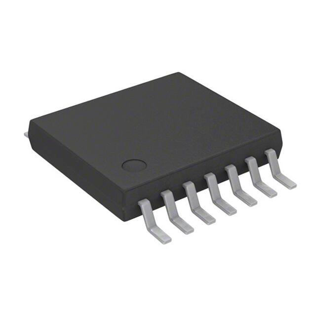


 工商网监
湘ICP备2023018690号
工商网监
湘ICP备2023018690号
