SST39VF3201C/SST39VF3202C
32-Mbit (x16) Multi-Purpose Flash Plus
The SST39VF3201C and SST39VF3202C devices are 2M x16, CMOS Multi-Purpose Flash Plus (MPF+) manufactured
with proprietary, high-performance CMOS SuperFlash® technology. The split-gate cell design and thick-oxide tunneling
injector attain better reliability and manufacturability compared with alternate approaches. The SST39VF3201C and
SST39VF3202C write (Program or Erase) with a 2.7V-3.6V power supply. This device conforms to JEDEC standard
pinouts for x16 memories.
Features
• Organized as 2M x16
• Single Voltage Read and Write Operations:
- 2.7V-3.6V
• Superior Reliability:
- Endurance: 100,000 Cycles (Typical)
- Greater than 100 years Data Retention
• Low-Power Consumption (typical values at
5 MHz):
- Active Current: 6 mA (typical)
- Standby Current: 4 µA (typical)
- Auto Low-Power Mode: 4 µA (typical)
• Hardware Block Protection/WP# Input Pin:
- Top Block Protection (top two 4-KWord
blocks)
for SST39VF3202C
- Bottom Block-Protection (bottom two 4KWord blocks) for SST39VF3201C
• Sector-Erase Capability:
- Uniform 2 KWord sectors
• Block-Erase Capability:
- Flexible block architecture
- Eight 4-KWord blocks, 63 32-KWord blocks
• Chip-Erase Capability
• Erase-Suspend/Erase-Resume Capabilities
• Hardware Reset Pin (RST#)
• Security-ID Feature:
- Microchip: 128 bits; User: 128 words
• Fast Read Access Time:
- 70 ns
• Latched Address and Data
2009-2020 Microchip Technology Inc.
• Fast Erase and Word-Program:
- Sector-Erase Time: 18 ms (typical)
- Block-Erase Time: 18 ms (typical)
- Chip-Erase Time: 35 ms (typical)
- Word-Program Time: 7 µs (typical)
• Automatic Write Timing:
- Internal VPP Generation
• End-of-Write Detection:
- Toggle Bits
- Data# Polling
- RY/BY# Pin
• CMOS I/O Compatibility
• JEDEC Standard:
- Flash EEPROM Pin Assignments
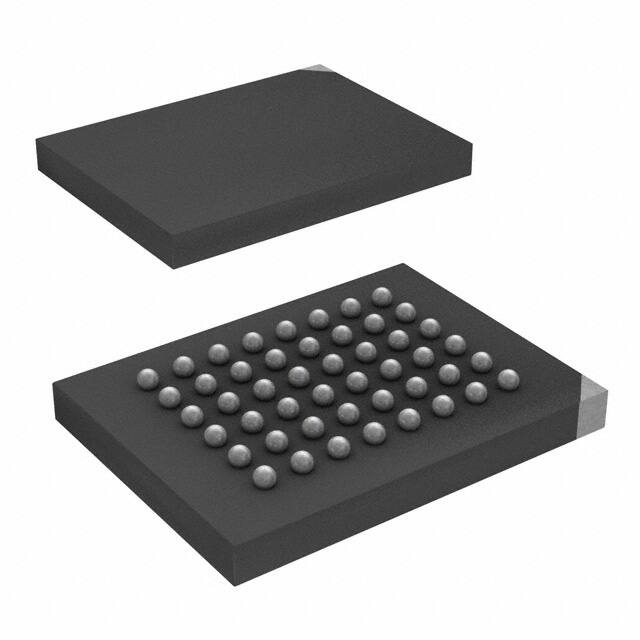
• Packages Available:
- 48-lead TSOP (12 mm x 20 mm)
- 48-ball TFBGA (6 mm x 8 mm)
• All devices are RoHS compliant
Packages
- 48-lead TSOP (12 mm x 20 mm)
- 48-ball TFBGA (6 mm x 8 mm)
DS20005020C-page 1
�SST39VF3201C/SST39VF3202C
DESCRIPTION
The SST39VF3201C and SST39VF3202C devices are 2M x16 CMOS Multi-Purpose Flash Plus (MPF+) manufactured
with proprietary, high-performance CMOS SuperFlash technology. The split-gate cell design and thick-oxide tunneling
injector attain better reliability and manufacturability compared with alternate approaches. The SST39VF3201C/
SST39VF3202C write (Program or Erase) with a 2.7V-3.6V power supply. These devices conform to JEDEC standard
pin assignments for x16 memories.
Featuring high-performance Word Program, the SST39VF3201C/SST39VF3202C devices provide a typical Word Program time of 7 µsec. These devices use Toggle Bit, Data# Polling or RY/BY# pin to indicate the completion of Program
operation. To protect against inadvertent write, they have on-chip hardware and Software Data Protection schemes.
Designed, manufactured and tested for a wide spectrum of applications, these devices are offered with a typical endurance of 100,000 cycles. Data retention is rated at greater than 100 years.
The SST39VF3201C/SST39VF3202C devices are suited for applications that require convenient and economical updating of program, configuration or data memory. For all system applications, they significantly improve performance and
reliability, while lowering power consumption. They inherently use less energy during Erase and Program than alternative Flash technologies. The total energy consumed is a function of the applied voltage, current and time of application.
Since for any given voltage range, the SuperFlash technology uses less current to program and has a shorter erase
time, the total energy consumed during any Erase or Program operation is less than alternative Flash technologies.
These devices also improve flexibility while lowering the cost for program, data and configuration storage applications.
The SuperFlash technology provides fixed Erase and Program times, independent of the number of Erase/Program
cycles that have occurred. Therefore, the system software or hardware does not have to be modified or derated as is
necessary with alternative Flash technologies, whose Erase and Program times increase with accumulated Erase/Program cycles.
To meet high-density, surface mount requirements, the SST39VF3201C/SST39VF3202C devices are offered in 48-lead
TSOP and 48-ball TFBGA packages. See Figure 2 and Figure 3 for pin assignments.
BLOCK DIAGRAM
FIGURE 1:
FUNCTIONAL BLOCK DIAGRAM
X-Decoder
Memory Address
SuperFlash
Memory
®
Address Buffer & Latches
CE#
OE#
WE#
WP#
RESET#
RY/BY#
Y-Decoder
Control Logic
I/O Buffers and Data Latches
DQ15 - DQ0
2009-2020 Microchip Technology Inc.
DS20005020C-page 2
�SST39VF3201C/SST39VF3202C
PIN DESCRIPTION
FIGURE 2:
PIN ASSIGNMENTS FOR 48-LEAD TSOP
A15
A14
A13
A12
A11
A10
A9
A8
A19
A20
WE#
RST#
NC
WP#
RY/BY#
A18
A17
A7
A6
A5
A4
A3
A2
A1
FIGURE 3:
1
2
3
4
5
6
7
8
9
10
11
12
13
14
15
16
17
18
19
20
21
22
23
24
Standard Pinout
Top View
Die Up
48
47
46
45
44
43
42
41
40
39
38
37
36
35
34
33
32
31
30
29
28
27
26
25
A16
NC
VSS
DQ15
DQ7
DQ14
DQ6
DQ13
DQ5
DQ12
DQ4
VDD
DQ11
DQ3
DQ10
DQ2
DQ9
DQ1
DQ8
DQ0
OE#
VSS
CE#
A0
PIN ASSIGNMENTS FOR 48-BALL TFBGA
TOP VIEW (balls facing down)
6
5
4
3
2
1
A13 A12 A14
A15 A16 NC DQ15 VSS
A8
A10
A11 DQ7 DQ14 DQ13 DQ6
WE# RST#
NC
A19 DQ5 DQ12 VDD DQ4
RY/BY# WP# A18
A20 DQ2 DQ10 DQ11 DQ3
A9
A7
A17
A6
A5
DQ0 DQ8 DQ9 DQ1
A3
A4
A2
A1
A0 CE# OE# VSS
A B C D E F G H
2009-2020 Microchip Technology Inc.
DS20005020C-page 3
�SST39VF3201C/SST39VF3202C
TABLE 1:
PIN DESCRIPTION
Symbol
Pin Name
Functions
AMS(1)-A0
Address Inputs
To provide memory addresses.
During Sector-Erase AMS-A11 address lines will select the sector.
During Block-Erase AMS-A15 address lines will select the block.
DQ15-DQ0
Data Input/output
To output data during Read cycles and receive input data during Write cycles.
Data is internally latched during a Write cycle.
The outputs are in tri-state when OE# or CE# is high.
WP#
Write-Protect
To protect the top/bottom boot block from Erase/Program operation when
grounded.
RST#
Reset
To reset and return the device to Read mode.
CE#
Chip Enable
To activate the device when CE# is low.
OE#
Output Enable
To gate the data output buffers.
WE#
Write Enable
To control the Write operations.
VDD
Power Supply
To provide power supply voltage: 2.7V-3.6V
VSS
Ground
NC
No Connection
Unconnected pins.
RY/BY#
Ready/Busy#
To output the status of a Program or Erase operation
RY/BY# is a open-drain output, so a 10 KW-100 KW pull-up resistor is required
to allow RY/BY# to transition high indicating the device is ready to read.
Note 1: AMS = Most Significant address.
AMS = A20 for SST39VF3201C/SST39VF3202C.
TABLE 2:
TOP/BOTTOM BOOT BLOCK ADDRESS
Top Boot Block Address SST39VF3202C
#
Size
(KWord)
70
69
Bottom Boot Block Address SST39VF3201C
Address Range
#
Size
(KWord)
Address Range
4
1FF000H-1FFFFFH
70
32
1F8000H-1FFFFFH
4
1FE000H-1FEFFFH
69
32
1F0000H-1F7FFFH
68
4
1FD000H-1FDFFFH
68
32
1E8000H-1EFFFFH
67
4
1FC000H-1FCFFFH
67
32
1E0000H-1E7FFFH
66
4
1FB000H-1FBFFFH
66
32
1D8000H-1DFFFFH
65
4
1FA000H-1FAFFFH
65
32
1D0000H-1D7FFFH
64
4
1F9000H-1F9FFFH
64
32
1C8000H-1CFFFFH
63
4
1F8000H-1F8FFFH
63
32
1C0000H-1C7FFFH
62
32
1F0000H-1F7FFFH
62
32
1B8000H-1BFFFFH
61
32
1E8000H-1EFFFFH
61
32
1B0000H-1B7FFFH
60
32
1E0000H-1E7FFFH
60
32
1A8000H-1AFFFFH
59
32
1D8000H-1DFFFFH
59
32
1A0000H-1A7FFFH
58
32
1D0000H-1D7FFFH
58
32
198000H-19FFFFH
57
32
1C8000H-1CFFFFH
57
32
190000H-197FFFH
56
32
1C0000H-1C7FFFH
56
32
188000H-18FFFFH
55
32
1B8000H-1BFFFFH
55
32
180000H-187FFFH
54
32
1B0000H-1B7FFFH
54
32
178000H-17FFFFH
53
32
1A8000H-1AFFFFH
53
32
170000H-177FFFH
52
32
1A0000H-1A7FFFH
52
32
168000H-16FFFFH
51
32
198000H-19FFFFH
51
32
160000H-167FFFH
2009-2020 Microchip Technology Inc.
DS20005020C-page 4
�SST39VF3201C/SST39VF3202C
TABLE 2:
TOP/BOTTOM BOOT BLOCK ADDRESS (CONTINUED)
Top Boot Block Address SST39VF3202C
Bottom Boot Block Address SST39VF3201C
50
32
190000H-197FFFH
50
32
158000H-15FFFFH
49
32
188000H-18FFFFH
49
32
150000H-157FFFH
48
32
180000H-187FFFH
48
32
148000H-14FFFFH
47
32
178000H-17FFFFH
47
32
140000H-147FFFH
46
32
170000H-177FFFH
46
32
138000H-13FFFFH
45
32
168000H-16FFFFH
45
32
130000H-137FFFH
44
32
160000H-167FFFH
44
32
128000H-12FFFFH
43
32
158000H-15FFFFH
43
32
120000H-127FFFH
42
32
150000H-157FFFH
42
32
118000H-11FFFFH
41
32
148000H-14FFFFH
41
32
110000H-117FFFH
40
32
140000H-147FFFH
40
32
108000H-10FFFFH
39
32
138000H-13FFFFH
39
32
100000H-107FFFH
38
32
130000H-137FFFH
38
32
0F8000H-0FFFFFH
37
32
128000H-12FFFFH
37
32
0F0000H-0F7FFFH
36
32
120000H-127FFFH
36
32
0E8000H-0EFFFFH
35
32
118000H-11FFFFH
35
32
0E0000H-0E7FFFH
34
32
110000H-117FFFH
34
32
0D8000H-0DFFFFH
33
32
108000H-10FFFFH
33
32
0D0000H-0D7FFFH
32
32
100000H-107FFFH
32
32
0C8000H-0CFFFFH
31
32
0F8000H-0FFFFFH
31
32
0C0000H-0C7FFFH
30
32
0F0000H-0F7FFFH
30
32
0B8000H-0BFFFFH
29
32
0E8000H-0EFFFFH
29
32
0B0000H-0B7FFFH
28
32
0E0000H-0E7FFFH
28
32
0A8000H-0AFFFFH
27
32
0D8000H-0DFFFFH
27
32
0A0000H-0A7FFFH
26
32
0D0000H-0D7FFFH
26
32
098000H-09FFFFH
25
32
0C8000H-0CFFFFH
25
32
090000H-097FFFH
24
32
0C0000H-0C7FFFH
24
32
088000H-08FFFFH
23
32
0B8000H-0BFFFFH
23
32
080000H-087FFFH
22
32
0B0000H-0B7FFFH
22
32
078000H-07FFFFH
21
32
0A8000H-0AFFFFH
21
32
070000H-077FFFH
20
32
0A0000H-0A7FFFH
20
32
068000H-06FFFFH
19
32
098000H-09FFFFH
19
32
060000H-067FFFH
18
32
090000H-097FFFH
18
32
058000H-05FFFFH
17
32
088000H-08FFFFH
17
32
050000H-057FFFH
16
32
080000H-087FFFH
16
32
048000H-04FFFFH
15
32
078000H-07FFFFH
15
32
040000H-047FFFH
14
32
070000H-077FFFH
14
32
038000H-03FFFFH
13
32
068000H-06FFFFH
13
32
030000H-037FFFH
12
32
060000H-067FFFH
12
32
028000H-02FFFFH
11
32
058000H-05FFFFH
11
32
020000H-027FFFH
10
32
050000H-057FFFH
10
32
018000H-01FFFFH
9
32
048000H-04FFFFH
9
32
010000H-017FFFH
8
32
040000H-047FFFH
8
32
008000H-00FFFFH
7
32
038000H-03FFFFH
7
4
007000H-007FFFH
2009-2020 Microchip Technology Inc.
DS20005020C-page 5
�SST39VF3201C/SST39VF3202C
TABLE 2:
TOP/BOTTOM BOOT BLOCK ADDRESS (CONTINUED)
Top Boot Block Address SST39VF3202C
Bottom Boot Block Address SST39VF3201C
6
32
030000H-037FFFH
6
4
006000H-006FFFH
5
32
028000H-02FFFFH
5
4
005000H-005FFFH
4
32
020000H-027FFFH
4
4
004000H-004FFFH
3
32
018000H-01FFFFH
3
4
003000H-003FFFH
2
32
010000H-017FFFH
2
4
002000H-002FFFH
1
32
008000H-00FFFFH
1
4
001000H-001FFFH
0
32
000000H-007FFFH
0
4
000000H-000FFFH
DEVICE OPERATION
Comments are used to initiate the memory operation functions of the device. Commands are written to the device using
standard microprocessor write sequences. A command is written by asserting WE# low while keeping CE# low. The
address bus is latched on the falling edge of WE# or CE#, whichever occurs last. The data bus is latched on the rising
edge of WE# or CE#, whichever occurs first.
The SST39VF3201C/SST39VF3202C also have the Auto-Low-Power mode which puts the device in a near Standby mode
after data has been accessed with a valid Read operation. This reduces the IDD active read current from typically 9 mA to typically
4 µA. The Auto-Low-Power mode reduces the typical IDD active read current to the range of 2 mA/MHz of Read cycle time. The
device exits the Auto-Low-Power mode with any address transition or control signal transition used to initiate another Read cycle,
with no access time penalty. Note that the device does not enter Auto-Low-Power mode after power-up with CE# held steadily
low, until the first address transition or CE# is driven high.
Read
The Read operation of the SST39VF3201C/SST39VF3202C is controlled by CE# and OE#, both have to be low for the system
to obtain data from the outputs. CE# is used for device selection. When CE# is high, the chip is deselected and only standby
power is consumed. OE# is the output control and is used to gate data from the output pins. The data bus is in high-impedance
state when either CE# or OE# is high. Refer to Figure 5 for further details.
Word Program Operation
The SST39VF3201C/SST39VF3202C are programmed on a word-by-word basis. Before programming, the sector where
the word exists must be fully erased. The Program operation is accomplished in three steps. The first step is the threebyte load sequence for Software Data Protection. The second step is to load word address and word data. During the
Word Program operation, the addresses are latched on the falling edge of either CE# or WE#, whichever occurs last.
The data is latched on the rising edge of either CE# or WE#, whichever occurs first. The third step is the internal Program
operation which is initiated after the rising edge of the fourth WE# or CE#, whichever occurs first. The Program operation, once initiated, will be completed within 10 µs. See Figure 6 and Figure 7 for WE# and CE# controlled Program
operation timing diagrams and Figure 21 for flowcharts. During the Program operation, the only valid reads are Data#
Polling and Toggle Bit. During the internal Program operation, the host is free to perform additional tasks. Any commands issued during the internal Program operation are ignored. During the command sequence, WP# should be statically held high or low.
2009-2020 Microchip Technology Inc.
DS20005020C-page 6
�SST39VF3201C/SST39VF3202C
Sector/Block-Erase Operation
The Sector- (or Block-) Erase operation allows the system to erase the device on a sector-by-sector (or block-by-block)
basis. The SST39VF3201C/SST39VF3202C offer both Sector-Erase and Block-Erase mode. The sector architecture is
based on uniform sector size of 2 KWord. The Block-Erase mode is based on block sizes of 4 and 32 KWord. The Sector-Erase operation is initiated by executing a six-byte command sequence with Sector-Erase command (50H) and sector address (SA) in the last bus cycle. The Block-Erase operation is initiated by executing a six-byte command sequence
with Block-Erase command (30H) and block address (BA) in the last bus cycle. The sector or block address is latched
on the falling edge of the sixth WE# pulse, while the command (50H or 30H) is latched on the rising edge of the sixth
WE# pulse. The internal Erase operation begins after the sixth WE# pulse. The End-of-Erase operation can be determined using either Data# Polling or Toggle Bit methods. See Figure 11 and Figure 12 for timing waveforms and
Figure 25 for the flowchart. Any commands issued during the Sector- or Block-Erase operation are ignored. When WP#
is low, any attempt to Sector- (Block-) Erase the protected block will be ignored. During the command sequence, WP#
should be statically held high or low.
Erase-Suspend/Erase-Resume Commands
The Erase-Suspend operation temporarily suspends a Sector- or Block-Erase operation thus allowing data to be read
from any memory location, or program data into any sector/block that is not suspended for an Erase operation. The
operation is executed by issuing one byte command sequence with Erase-Suspend command (B0H). The device automatically enters Read mode typically within 10 µs after the Erase-Suspend command had been issued. Valid data can
be read from any sector or block that is not suspended from an Erase operation. Reading at address location within
erase-suspended sectors/blocks will output DQ2 toggling and DQ6 at ‘1’. While in Erase-Suspend mode, a Word-Program operation is allowed except for the sector or block selected for Erase-Suspend.
To resume Sector-Erase or Block-Erase operation that has been suspended, the system must issue a Erase Resume
command. The operation is executed by issuing one byte command sequence with Erase Resume command (30H) at
any address in the last Byte sequence.
Chip-Erase Operation
The SST39VF3201C/SST39VF3202C provide a Chip-Erase operation, which allows the user to erase the entire memory array to the ‘1’ state. This is useful when the entire device must be quickly erased.
The Chip-Erase operation is initiated by executing a six-byte command sequence with Chip-Erase command (10H) at
address 555H in the last byte sequence. The Erase operation begins with the rising edge of the sixth WE# or CE#,
whichever occurs first. During the Erase operation, the only valid read is Toggle Bit or Data# Polling. See Table 7 for the
command sequence, Figure 10 for timing diagram and Figure 25 for the flowchart. Any commands issued during the
Chip-Erase operation are ignored. When WP# is low, any attempt to Chip-Erase will be ignored. During the command
sequence, WP# should be statically held high or low.
Write Operation Status Detection
The SST39VF3201C/SST39VF3202C provide two software means to detect the completion of a Write (Program or Erase)
cycle, in order to optimize the system write cycle time. The software detection includes two Status bits: Data# Polling
(DQ7) and Toggle Bit (DQ6). The End-of-Write Detection mode is enabled after the rising edge of WE#, which initiates
the internal Program or Erase operation.
The actual completion of the nonvolatile write is asynchronous with the system; therefore, either a Data# Polling or Toggle Bit read may be simultaneous with the completion of the write cycle. If this occurs, the system may possibly get an
erroneous result (i.e., valid data may appear to conflict with either DQ7 or DQ6). In order to prevent spurious rejection,
if an erroneous result occurs, the software routine should include a loop to read the accessed location an additional two
(2) times. If both reads are valid, then the device has completed the Write cycle, otherwise the rejection is valid.
Data# Polling (DQ7)
When the SST39VF3201C/SST39VF3202C are in the internal Program operation, any attempt to read DQ7 will produce
the complement of the true data. Once the Program operation is completed, DQ7 will produce true data. Note that even
though DQ7 may have valid data immediately following the completion of an internal Write operation, the remaining data outputs
may still be invalid: valid data on the entire data bus will appear in subsequent successive Read cycles after an interval of 1 µs.
During internal Erase operation, any attempt to read DQ7 will produce a ‘0’. Once the internal Erase operation is com-
2009-2020 Microchip Technology Inc.
DS20005020C-page 7
�SST39VF3201C/SST39VF3202C
pleted, DQ7 will produce a ‘1’. The Data# Polling is valid after the rising edge of fourth WE# (or CE#) pulse for Program
operation. For Sector-, Block- or Chip-Erase, the Data# Polling is valid after the rising edge of sixth WE# (or CE#) pulse.
See Figure 8 for Data# Polling timing diagram and Figure 22 for a flowchart.
Toggle Bits (DQ6 and DQ2)
During the internal Program or Erase operation, any consecutive attempts to read DQ6 will produce alternating ‘1’s and
‘0’s (i.e., toggling between ‘1’ and ‘0’.) When the internal Program or Erase operation is completed, the DQ6 bit will stop
toggling. The device is then ready for the next operation. For Sector-, Block-, or Chip-Erase, the toggle bit (DQ6) is valid
after the rising edge of sixth WE# (or CE#) pulse. DQ6 will be set to ‘1’ if a Read operation is attempted on an EraseSuspended Sector/Block. If Program operation is initiated in a sector/block not selected in Erase-Suspend mode, DQ6
will toggle.
An additional Toggle Bit is available on DQ2, which can be used in conjunction with DQ6 to check whether a particular
sector is being actively erased or erase-suspended. Table 3 shows detailed Status bits information. The Toggle Bit (DQ2)
is valid after the rising edge of the last WE# (or CE#) pulse of Write operation. See Figure 9 for Toggle Bit timing diagram
and Figure 22 for a flowchart.
TABLE 3:
WRITE OPERATION STATUS
DQ7(1)
DQ6(1)
DQ2(1)
RY/BY#
DQ7#
Toggle
No Toggle
0
Toggle
Toggle
0
1
1
Toggle
Read from Non- Erase-Suspended Sector/
Block
Data
Data
Data
Program
DQ7#
Toggle
N/A
Status
Normal Operation
Standard Program
Standard Erase
Erase-Suspend Mode Read from Erase-Suspended Sector/Block
Note 1: DQ7, DQ6 and DQ2 require a valid address when reading status information.
0
1
1
0
Ready/Busy# (RY/BY#)
The devices include a Ready/Busy# (RY/BY#) output signal. RY/BY# is an open-drain output pin that indicates whether
an Erase or Program operation is in progress. Since RY/BY# is an open-drain output, it allows several devices to be tied
in parallel to VDD via an external pull-up resistor. After the rising edge of the final WE# pulse in the command sequence,
the RY/BY# status is valid.
When RY/BY# is actively pulled low, it indicates that an Erase or Program operation is in progress. When RY/BY# is
high (Ready), the devices may be read or left in Standby mode.
Data Protection
The SST39VF3201C/SST39VF3202C provide both hardware and software features to protect nonvolatile data from inadvertent writes.
Hardware Data Protection
Noise/Glitch Protection: A WE# or CE# pulse of less than 5 ns will not initiate a write cycle.
VDD Power Up/Down Detection: The Write operation is inhibited when VDD is less than 1.5V.
Write Inhibit Mode: Forcing OE# low, CE# high, or WE# high will inhibit the Write operation.
This prevents inadvertent writes during power-up or power-down.
Hardware Block Protection
The SST39VF3202C supports top hardware block protection, which protects the top two 4-KWord blocks of the device.
The SST39VF3201C supports bottom hardware block protection, which protects the bottom two 4-KWord blocks of the
device. The Boot Block address ranges are described in Table 4. Program and Erase operations are prevented on the
two 4-KWord blocks when WP# is low. If WP# is left floating, it is internally held high via a pull-up resistor, and the Boot
Block is unprotected, enabling Program and Erase operations on that block.
2009-2020 Microchip Technology Inc.
DS20005020C-page 8
�SST39VF3201C/SST39VF3202C
TABLE 4:
BOOT BLOCK ADDRESS RANGES
Product
Address Range
Bottom Boot Block
SST39VF3201C
000000H-001FFFH
Top Boot Block
SST39VF3202C
1FE000H-1FFFFFH
Hardware Reset (RST#)
The RST# pin provides a hardware method of resetting the device to read array data. When the RST# pin is held low
for at least TRP, any in-progress operation will terminate and return to Read mode. When no internal Program/Erase
operation is in progress, a minimum period of TRHR is required after RST# is driven high before a valid Read can take
place. See Figure 17.
The Erase or Program operation that has been interrupted needs to be re-initiated after the device resumes normal
operation mode to ensure data integrity.
Software Data Protection (SDP)
The SST39VF3201C/SST39VF3202C provide the JEDEC approved Software Data Protection scheme for all data alteration operations (i.e., Program and Erase). Any Program operation requires the inclusion of the three-byte sequence.
The three-byte load sequence is used to initiate the Program operation, providing optimal protection from inadvertent
Write operations (e.g., during the system power-up or power-down). Any Erase operation requires the inclusion of sixbyte sequence. These devices are shipped with the Software Data Protection permanently enabled. See Table 7 for the
specific software command codes. During the SDP command sequence, invalid commands will abort the device to Read
mode within TRC. The contents of DQ15-DQ8 can be VIL or VIH, but no other value, during any SDP command sequence.
Common Flash Memory Interface (CFI)
The SST39VF3201C/SST39VF3202C also contain the CFI information to describe the characteristics of the device. In
order to enter the CFI Query mode, the system must write the three-byte sequence, same as product ID entry command
with 98H (CFI Query command) to address 555H in the last byte sequence. The system can also enter the CFI Query
mode, by using the one-byte sequence with 55H on Address and 98H on Data Bus. Once the device enters the CFI
Query mode, the system can read CFI data at the addresses given in Table 9 through Table 11. The system must write
the CFI Exit command to return to Read mode from the CFI Query mode.
Product Identification
The Product Identification mode identifies the devices as the SST39VF3201C and SST39VF3202C and the manufacturer as Microchip. This mode may be accessed through software operations. Users may use the Software Product
Identification operation to identify the part (i.e., using the device ID) when using multiple manufacturers in the same
socket. For details, see Table 7 for software operation, Figure 13 for the Software ID Entry and Read timing diagram
and Figure 23 for the Software ID Entry command sequence flowchart.
TABLE 5:
PRODUCT IDENTIFICATION
Manufacturer’s ID
Device ID
Address
Data
0000H
BFH
l
SST39VF3201C
0001H
235F
SST39VF3202C
0001H
235E
2009-2020 Microchip Technology Inc.
DS20005020C-page 9
�SST39VF3201C/SST39VF3202C
Product Identification Mode Exit/CFI Mode Exit
In order to return to the standard Read mode, the Software Product Identification mode must be exited. Exit is accomplished by issuing the Software ID Exit command sequence, which returns the device to the Read mode. This command
may also be used to reset the device to the Read mode after any inadvertent transient condition that apparently causes
the device to behave abnormally (e.g., not read correctly). Note that the Software ID Exit/CFI Exit command is ignored
during an internal Program or Erase operation. See Table 7 for software command codes, Figure 15 for timing waveform
and Figure 23 and Figure 24 for flowcharts.
Security ID
The SST39VF3201C/SST39VF3202C devices offer a 136-word Security ID space. The Secure ID space is divided into
two segments - one factory-programmed segment and one user-programmed segment. The first segment is programmed and locked at Microchip with a random 128-bit number.
The 128-word user segment is left unprogrammed for the customer to program as desired.
To program the user segment of the Security ID, the user must use the Security ID Word-Program command. To detect
end-of-write for the SEC ID, read the toggle bits. Do not use Data# Polling. Once this is complete, the Sec ID should be
locked using the User Sec ID Program Lock-Out. This disables any future corruption of this space. Note that regardless
of whether or not the Sec ID is locked, neither Sec ID segment can be erased.
The Secure ID space can be queried by executing a three-byte command sequence with Enter Sec ID command (88H)
at address 555H in the last byte sequence. To exit this mode, the Exit Sec ID command should be executed. Refer to
Table 7 for more details.
OPERATIONS
TABLE 6:
OPERATION MODES SELECTION
Mode
CE#
OE#
WE#
DQ
Address
Read
VIL
VIL
VIH
DOUT
AIN
Program
VIL
VIH
VIL
DIN
AIN
Erase
VIL
VIH
VIL
Standby
VIH
X
X
Write Inhibit
Sector or block address, XXH for Chip-Erase
High-Z
X
X
VIL
X
High-Z/ DOUT X
X
X
VIH
High-Z/ DOUT X
VIL
VIL
VIH
Product Identification
Software Mode
See Table 7
Note 1: X can be VIL or VIH, but no other value.
2009-2020 Microchip Technology Inc.
DS20005020C-page 10
�SST39VF3201C/SST39VF3202C
TABLE 7:
SOFTWARE COMMAND SEQUENCE
Command
Sequence
1st Bus Write
Cycle
Addr(1)
2nd Bus Write
Cycle
Data(2) Addr(1)
3rd Bus Write
Cycle
4th Bus Write
Cycle
5th Bus Write
Cycle
6th Bus Write
Cycle
Data(2) Addr(1) Data(2) Addr(1) Data(2) Addr(1) Data(2) Addr(1) Data(2)
Word Program
555H
AAH
2AAH
55H
555H
A0H
WA(3)
Data
Sector Erase
555H
AAH
2AAH
55H
555H
80H
555H
AAH
2AAH
55H
Block Erase
555H
AAH
2AAH
55H
555H
80H
555H
AAH
2AAH
55H
BAX(4)
Chip Erase
555H
AAH
2AAH
55H
555H
80H
555H
AAH
2AAH
55H
555H
Erase Suspend
XXXXH
B0H
Erase Resume
XXXXH
30H
Query Sec ID
(5)
555H
AAH
2AAH
55H
555H
88H
User Security ID
Word Program
555H
AAH
2AAH
55H
555H
A5H
WA(6)
Data
User Security ID
Program LockOut
555H
AAH
2AAH
55H
555H
85H
XXH(6)
0000H
Software ID
Entry(7,8)
555H
AAH
2AAH
55H
555H
90H
CFI Query Entry
555H
AAH
2AAH
55H
555H
98H
CFI Query Entry
55H
98H
Software ID
Exit(9,10)/CFI Exit/
Sec ID Exit
555H
AAH
2AAH
55H
555H
F0H
Software ID
Exit(9,10)/CFI Exit/
Sec ID Exit
XXH
F0H
2009-2020 Microchip Technology Inc.
SAX(4)
DS20005020C-page 11
50H
30H
10H
�SST39VF3201C/SST39VF3202C
TABLE 7:
SOFTWARE COMMAND SEQUENCE
Command
Sequence
1st Bus Write
Cycle
Addr(1)
2nd Bus Write
Cycle
Data(2) Addr(1)
3rd Bus Write
Cycle
4th Bus Write
Cycle
5th Bus Write
Cycle
6th Bus Write
Cycle
Data(2) Addr(1) Data(2) Addr(1) Data(2) Addr(1) Data(2) Addr(1) Data(2)
Note 1: Address format A10-A0 (Hex).
Addresses A11- A20 can be VIL or VIH, but no other value, for Command sequence for SST39VF3201C/
SST39VF3202C.
2: DQ15-DQ8 can be VIL or VIH, but no other value, for Command sequence.
3: WA = Program Word Address
4: SAX for Sector-Erase; uses AMS-A11 address lines
BAX, for Block-Erase; uses AMS-A15 address lines
AMS = Most Significant address
AMS = A20 for SST39VF3201C/SST39VF3202C
5: With AMS-A4 = 0;Sec ID is read with A3-A0,
Microchip ID is read with A3 = 0 (Address range = 000000H to 000007H),
User ID is read with A3 = 1 (Address range = 000008H to 000087H).
Lock Status is read with A7-A0 = 0000FFH. Unlocked: DQ3 = 1 / Locked: DQ3 = 0.
6: Valid Word Addresses for Sec ID are from 000000H-000007H and 000008H to 000087H.
7: The device does not remain in Software Product ID mode if powered down.
8: For Manufacture ID
With AMS-A0 =0;Microchip Manufacturer ID = 00BFH is read
For Device ID Device ID can be read in one cycle (address 01H)
One-cycle method With AMS-A1=0, A0=1; Microchip39VF3201C/3202C Device ID = 235F/235E is read
AMS = Most Significant address
AMS = A20 for SST39VF3201C/SST39VF3202C
9: Both Software ID Exit operations are equivalent
10: If users never lock after programming, Sec ID can be programmed over the previously unprogrammed bits (data=1)
using the Sec ID mode again (the programmed ‘0’ bits cannot be reversed to ‘1’). Valid Word-Addresses for Sec ID are
from 000000H-000007H and 000008H to 000087H.
TABLE 8:
CFI QUERY IDENTIFICATION STRING (1) FOR SST39VF3201C/SST39VF3202C
Address
Data
10H
0051H
11H
0052H
12H
0059H
13H
0002H
14H
0000H
15H
0000H
16H
0000H
17H
0000H
18H
0000H
19H
0000H
1AH
0000H
Data
Query Unique ASCII string “QRY”
Primary OEM command set
Address for Primary Extended Table
Alternate OEM command set (00H = none exists)
Address for Alternate OEM extended Table (00H = none exits)
Note 1: Refer to CFI publication 100 for more details.
2009-2020 Microchip Technology Inc.
DS20005020C-page 12
�SST39VF3201C/SST39VF3202C
TABLE 9:
SYSTEM INTERFACE INFORMATION FOR SST39VF3201C/SST39VF3202C
Address
Data
Data
1BH
0027H
VDD Min (Program/Erase); DQ7-DQ4: Volts, DQ3-DQ0: 100 millivolts
1CH
0036H
VDD Max (Program/Erase); DQ7-DQ4: Volts, DQ3-DQ0: 100 millivolts
1DH
0000H
VPP min. (00H = no VPP pin)
1EH
0000H
1FH
0003H
20H
0000H
21H
0004H
22H
0005H
23H
0001H
24H
0000H
25H
0001H
26H
0001H
TABLE 10:
VPP max. (00H = no VPP pin)
Typical time out for Word-Program 2N µs (23 = 8 µs)
Typical time out for min. size buffer program 2N µs (00H = not supported)
Typical time out for individual Sector/Block-Erase 2N ms (24 = 16 ms)
Typical time out for Chip-Erase 2N ms (25 = 32 ms)
Maximum time out for Word-Program 2N times typical (21 x 23 = 16 µs)
Maximum time out for buffer program 2N times typical
Maximum time out for individual Sector/Block-Erase 2N times typical (21 x 24 = 32 ms)
Maximum time out for Chip-Erase 2N times typical (21 x 25 = 64 ms)
DEVICE GEOMETRY FOR SST39VF3201C/SST39VF3202C
Address
Data
27H
0016H
Device size = 2N Bytes (16H = 22; 222 = 4MByte)
28H
0001H
Flash Device Interface description; 0001H = x16-only asynchronous interface
29H
0000H
2AH
0000H
2BH
0000H
2CH
0003H
Number of Erase Sector/Block sizes supported by device
2DH
0007H
Erase Block1 region information
2EH
0000H
2FH
0020H
30H
0000H
31H
003EH
32H
0000H
33H
0000H
34H
0001H
35H
0000H
36H
0000H
37H
0000H
38H
0000H
39H
0000H
3AH
0000H
3BH
0000H
3CH
0000H
2009-2020 Microchip Technology Inc.
Data
Maximum number of bytes in multi-byte write = 2N (00H = not supported)
Erase Block2 region information
Erase Block3 region information
Erase Block4 region information
DS20005020C-page 13
�SST39VF3201C/SST39VF3202C
Absolute Maximum Stress Ratings (Applied conditions greater than those listed under “Absolute Maximum Stress Ratings” may cause permanent damage to the device. This is a stress rating only and functional operation of the device at
these conditions or conditions greater than those defined in the operational sections of this data sheet is not implied. Exposure to absolute maximum stress rating conditions may affect device reliability.)
Temperature Under Bias ......................................................................................................................... -55°C to +125°C
Storage Temperature ............................................................................................................................. --65°C to +150°C
D. C. Voltage on Any Pin to Ground Potential .....................................................................................-0.5V to VDD+0.5V
Transient Voltage ( 100 μs
VDD min
VDD
0V
VIH
RESET#
TRHR > 50 ns
CE#
TABLE 13:
DC OPERATING CHARACTERISTICS VDD = 2.7V-3.6V(1)
Symbol
IDD
Parameter
Limits
Min
Max
Units
Test Conditions
Address Input = VILT/VIHT(2) at f = 5 MHz,
VDD = VDD Max
Power Supply Current
Read(3)
15
mA
CE#=VIL, OE#=WE#=VIH, all I/Os open
Program and Erase
45
mA
CE#=WE#=VIL, OE#=VIH
ISB
Standby VDD Current
50
µA
CE#=VIHC, VDD=VDD Max
IALP
Auto Low Power
50
µA
CE#=VILC, VDD=VDD Max
All inputs=VSS or VDD, WE#=VIHC
ILI
Input Leakage Current
1
µA
VIN=GND to VDD, VDD=VDD Max
ILIW
Input Leakage Current
on WP# pin and RST#
10
µA
WP#=GND to VDD or RST#=GND to VDD
ILO
Output Leakage Current
1
µA
VOUT=GND to VDD, VDD=VDD Max
VIL
Input Low Voltage
0.8
V
VDD=VDD Min
VILC
Input Low Voltage (CMOS)
0.3
V
VDD=VDD Max
VIH
Input High Voltage
0.7VDD
V
VDD=VDD Max
VIHC
Input High Voltage (CMOS)
VDD0.3
V
VDD=VDD Max
VOL
Output Low Voltage
V
IOL=100 µA, VDD=VDD Min
VOH
Output High Voltage
V
IOH=-100 µA, VDD=VDD Min
0.2
VDD0.2
Note 1: Typical conditions for the Active Current shown on the front page of the data sheet are average values at
25°C (room temperature), and VDD = 3V. Not 100% tested.
2: See Figure 19.
3: The IDD current listed is typically less than 2 mA/MHz, with OE# at VIH. Typical VDD is 3V.
2009-2020 Microchip Technology Inc.
DS20005020C-page 15
�SST39VF3201C/SST39VF3202C
TABLE 14:
RECOMMENDED SYSTEM POWER-UP TIMINGS
Symbol
TPU-READ(1)
TPU-WRITE(1)
Parameter
Minimum
Units
Power-up to Read Operation
100
µs
Power-up to Program/Erase Operation
100
µs
Note 1: This parameter is measured only for initial qualification and after a design or process change that could
affect this parameter.
TABLE 15:
CAPACITANCE (TA = 25°C, F = 1 MHZ, OTHER PINS OPEN)
Parameter
CI/O(1)
CIN(1)
Description
Test Condition
Maximum
I/O Pin Capacitance
VI/O = 0V
10 pF
Input Capacitance
VIN = 0V
10 pF
Note 1: This parameter is measured only for initial qualification and after a design or process change that could
affect this parameter.
TABLE 16:
Symbol
RELIABILITY CHARACTERISTICS
Parameter
NEND(1,2)
DR(1)
Endurance
ILTH(1)
Latch-Up
T
Minimum Specification
Units
10,000
Cycles
JEDEC Standard A117
100
Years
JEDEC Standard A103
100 - IDD
mA
JEDEC Standard 78
Data Retention
Test Method
Note 1: This parameter is measured only for initial qualification and after a design or process change that could
affect this parameter.
2: NEND endurance rating is qualified as a 10,000 cycle minimum for the whole device, A sector- or blocklevel rating would result in higher minimum specification.
AC CHARACTERISTICS
TABLE 17:
READ CYCLE TIMING PARAMETERS VDD = 2.7V-3.6V
Symbol
Parameter
Min
Max
TRC
Read Cycle Time
TCE
Chip Enable Access Time
70
ns
TAA
Address Access Time
70
ns
TOE
Output Enable Access Time
35
ns
TCLZ(1)
OLZ(1)
T
TCHZ(1)
OHZ(1)
T
TOH(1)
RP(1)
T
TRHR(1)
RY(1,2)
T
70
Units
ns
CE# Low to Active Output
0
ns
OE# Low to Active Output
0
ns
CE# High to High-Z Output
16
ns
OE# High to High-Z Output
16
ns
Output Hold from Address Change
0
ns
RST# Pulse Width
500
ns
RST# High before Read
50
RST# Pin Low to Read Mode
ns
20
µs
Note 1: This parameter is measured only for initial qualification and after a design or process change that could
affect this parameter.
2: This parameter applies to Sector-Erase, Block-Erase and Program operations. This parameter does not
apply to Chip-Erase operations.
2009-2020 Microchip Technology Inc.
DS20005020C-page 16
�SST39VF3201C/SST39VF3202C
TABLE 18:
PROGRAM/ERASE CYCLE TIMING PARAMETERS
Symbol
Parameter
TBP
Word-Program Time
Min
Max
Units
10
µs
TAS
Address Setup Time
0
ns
TAH
Address Hold Time
30
ns
TCS
WE# and CE# Setup Time
0
ns
TCH
WE# and CE# Hold Time
0
ns
TOES
OE# High Setup Time
0
ns
TOEH
OE# High Hold Time
10
ns
TCP
CE# Pulse Width
40
ns
TWP
WE# Pulse Width
40
ns
WE# Pulse Width High
30
ns
CE# Pulse Width High
30
ns
Data Setup Time
30
ns
Data Hold Time
0
ns
TWPH(1)
TCPH(1)
TDS
TDH(1)
TIDA(1)
Software ID Access and Exit Time
150
ns
TSE
Sector-Erase
25
ms
TBE
Block-Erase
25
ms
TSCE
Chip-Erase
50
ms
0
µs
TBY(1,2)
BR(1)
RY/BY# Delay Time
90
ns
Bus Recovery Time
T
Note 1: This parameter is measured only for initial qualification and after a design or process change that could
affect this parameter.
2: This parameter applies to Sector-Erase, Block-Erase and Program operations.
FIGURE 5:
READ CYCLE TIMING DIAGRAM
TRC
TAA
ADDRESS AMS-0
TCE
CE#
TOE
OE#
VIH
TOHZ
TOLZ
WE#
TCLZ
DQ15-0
HIGH-Z
TOH
DATA VALID
TCHZ
DATA VALID
HIGH-Z
Note 1: AMS = Most Significant address
AMS = A20 for SST39VF3201C/SST39VF3202C
2009-2020 Microchip Technology Inc.
DS20005020C-page 17
�SST39VF3201C/SST39VF3202C
FIGURE 6:
WE# CONTROLLED PROGRAM CYCLE TIMING DIAGRAM
TBP
ADDRESSES
555
2AA
555
ADDR
TAH
TWP
WE#
TWPH
TAS
OE#
TCH
CE#
TCS
TBY
TBR
RY/BY#
TDS
DQ15-0
XXAA
XX55
XXA0
TDH
DATA
VALID
WORD
(ADDR/DATA)
Note 1: WP# must be held in proper logic state (VIL or VIH) 1 µs prior to and 1 µs after the command sequence.
X can be VIL or VIH, but no other value.
FIGURE 7:
CE# CONTROLLED PROGRAM CYCLE TIMING DIAGRAM
TBP
ADDRESSES
555
2AA
555
ADDR
TAH
TCP
WE#
TAS
TCPH
OE#
TCH
CE#
TCS
TBY
TBR
RY/BY#
TDS
DQ15-0
XXAA
XX55
XXA0
DATA
TDH
VALID
WORD
(ADDR/DATA)
Note 1: WP# must be held in proper logic state (VIL or VIH) 1 µs prior to and 1 µs after the command sequence.
X can be VIL or VIH, but no other value.
2009-2020 Microchip Technology Inc.
DS20005020C-page 18
�SST39VF3201C/SST39VF3202C
FIGURE 8:
DATA# POLLING TIMING DIAGRAM
ADDRESS A19-0-AMS-0
TCE
CE#
TOEH
TOES
OE#
TOE
WE#
TBY
RY/BY#
DQ7
DATA#
DATA
DATA#
DATA
Note 1: AMS = Most Significant address
2: AMS = A20 for SST39VF3201C/SST39VF3202C
FIGURE 9:
TOGGLE BITS TIMING DIAGRAM
ADDRESS AMS-0
TCE
CE#
TOEH
TOES
TOE
OE#
WE#
DQ6 and DQ2
TWO READ CYCLES
WITH SAME OUTPUTS
Note 1: AMS = Most Significant address
2: AMS = A20 for SST39VF3201C/SST39VF3202C
2009-2020 Microchip Technology Inc.
DS20005020C-page 19
�SST39VF3201C/SST39VF3202C
FIGURE 10:
WE# CONTROLLED CHIP ERASE TIMING DIAGRAM
TSCE
SIX-BYTE CODE FOR CHIP-ERASE
ADDRESSES
555
2AA
555
555
2AA
555
CE#
OE#
TOEH
WE#
TBY
TBR
RY/BY#
DQ15-0
XXAA
XX55
XX80
XXAA
XX55
XX10
VALID
Note 1: This device also supports CE# controlled Chip Erase operation. The WE# and CE# signals are interchangeable as long
as minimum timings are met. (see Table 18)
WP# must be held in proper logic state (VIL or VIH) 1 µs prior to and 1 µs after the command sequence.
X can be VIL or VIH, but no other value.
FIGURE 11:
WE# CONTROLLED BLOCK ERASE TIMING DIAGRAM
TBE
SIX-BYTE CODE FOR BLOCK-ERASE
ADDRESSES
555
2AA
555
555
2AA
BAX
CE#
OE#
TWP
WE#
TBY
TBR
RY/BY#
DQ15-0
Note 1:
XXAA
XX55
XX80
XXAA
XX55
XX30
VALID
This device also supports CE# controlled Block Erase operation. The WE# and CE# signals are interchangeable as long
as minimum timings are met. (see Table 18)
WP# must be held in proper logic state (VIL or VIH) 1 µs prior to and 1 µs after the command sequence.
X can be VIL or VIH, but no other value.
2009-2020 Microchip Technology Inc.
DS20005020C-page 20
�SST39VF3201C/SST39VF3202C
FIGURE 12:
WE# CONTROLLED SECTOR ERASE TIMING DIAGRAM
TSE
SIX-BYTE CODE FOR SECTOR-ERASE
ADDRESSES
555
2AA
555
555
2AA
SAX
CE#
OE#
TWP
WE#
TBY
TBR
RY/BY#
DQ15-0
XXAA
XX55
XX80
XXAA
XX55
XX50
VALID
2: This device also supports CE# controlled Sector Erase operation The WE# and CE# signals are interchangeable as long
as minimum timings are met. (see Table 18)
SAX = Block Address
WP# must be held in proper logic state (VIL or VIH) 1 µs prior to and 1 µs after the command sequence.
X can be VIL or VIH, but no other value.
FIGURE 13:
SOFTWARE ID ENTRY AND READ
Three-Byte Sequence for Software ID Entry
ADDRESS
555
2AA
555
0000
0001
CE#
OE#
TIDA
TWP
WE#
TWPH
DQ15-0
TAA
XXAA
XX55
XX90
SW0
SW1
SW2
00BF
Device ID
Note 1: Device ID = 235E for SST39VF3201C and 235E for SST39VF3202C.
WP# must be held in proper logic state (VIL or VIH) 1 µs prior to and 1 µs after the command sequence.
X can be VIL or VIH, but no other value.
2009-2020 Microchip Technology Inc.
DS20005020C-page 21
�SST39VF3201C/SST39VF3202C
FIGURE 14:
CFI QUERY AND READ
Three-Byte Sequence for CFI Query Entry
555
ADDRESS
2AA
555
CE#
OE#
TIDA
TWP
WE#
TWPH
DQ15-0
TAA
XXAA
XX55
XX98
SW0
SW1
SW2
Note 1: WP# must be held in proper logic state (VIL or VIH) 1 µs prior to and 1 µs after the command sequence.
X can be VIL or VIH, but no other value.
FIGURE 15:
SOFTWARE ID EXIT/CFI EXIT
THREE-BYTE SEQUENCE FOR
SOFTWARE ID EXIT AND RESET
ADDRESS A14-0
DQ15-0
555
2AA
XXAA
555
XX55
XXF0
TIDA
CE#
OE#
TWP
WE#
TWHP
SW0
SW1
SW2
Note 1: WP# must be held in proper logic state (VIL or VIH) 1 µs prior to and 1 µs after the command sequence.
X can be VIL or VIH, but no other value.
2009-2020 Microchip Technology Inc.
DS20005020C-page 22
�SST39VF3201C/SST39VF3202C
FIGURE 16:
SEC ID ENTRY
THREE-BYTE SEQUENCE FOR
CFI QUERY ENTRY
ADDRESS AMS-0
555
2AA
555
CE#
OE#
TIDA
TWP
WE#
TWPH
DQ15-0
TAA
XXAA
XX55
XX88
SW0
SW1
SW2
Note 1: AMS = Most Significant address
AMS = A20 for SST39VF3201C/SST39VF3202C
WP# must be held in proper logic state (VIL or VIH) 1 µs prior to and 1 µs after the command sequence.
X can be VIL or VIH, but no other value.
FIGURE 17:
RST# TIMING DIAGRAM (WHEN NO INTERNAL OPERATION IS IN PROGRESS)
RY/BY#
0V
TRP
RST#
TRHR
CE#/OE#
2009-2020 Microchip Technology Inc.
DS20005020C-page 23
�SST39VF3201C/SST39VF3202C
FIGURE 18:
RST# TIMING DIAGRAM (DURING PROGRAM OR ERASE OPERATION)
TRY
RY/BY#
TRP
RST#
CE#
TBR
OE#
FIGURE 19:
AC INPUT/OUTPUT REFERENCE WAVEFORMS
VIHT
VIT
INPUT
REFERENCE POINTS
VOT
OUTPUT
VILT
AC test inputs are driven at VIHT (0.9 VDD) for a logic ‘1’ and VILT (0.1 VDD) for a logic ‘0’. Measurement reference
points for inputs and outputs are VIT (0.5 VDD) and VOT (0.5 VDD). Input rise and fall times (10% 90%) are


 工商网监
湘ICP备2023018690号
工商网监
湘ICP备2023018690号
