UPS1040e3
10 A LOW VF Schottky BARRIER RECTIFIER
SCOTTSDALE DIVISION
KEY FEATURES
DESCRIPTION
This UPS1040e3 in the Powermite3 package is a high efficiency Schottky rectifier
that is also RoHS compliant offering high current/power capabilities previously
found only in much larger packages. They are ideal for SMD applications that
operate at high frequencies. In addition to its size advantages, the Powermite3®
package includes a full metallic bottom that eliminates the possibility of solder flux
entrapment during assembly and a unique locking tab act as an efficient heat path to
the heat-sink mounting. Its innovative design makes this device ideal for use with
automatic insertion equipment.
IMPORTANT: For the most current data, consult MICROSEMI’s website: http://www.microsemi.com
ABSOLUTE MAXIMUM RATINGS AT 25º C
(UNLESS OTHERWISE SPECIFIED)
Rating
Symbol
Value
Unit
Peak Repetitive Reverse Voltage
Working Peak Reverse Voltage
DC Blocking Voltage
VRRM
VRWM
VR
40
V
RMS Reverse Voltage
V R (RMS)
28
V
Average Rectified Output Current
Non-Repetitive Peak Forward Surge Current
8.3 ms Single half sine wave Superimposed
on Rated Load@ Tc =90ºC
Storage Temperature
Io
10
A
IFSM
150
A
TSTG
-55 to +150
ºC
Junction Temperature
TJ
-55 to +150
ºC
THERMAL CHARACTERISTICS
Thermal Resistance
Junction-to-case (bottom)
Junction to ambient (1)
RθJC
RθJA
APPLICATIONS/BENEFITS
Switching and Regulating Power
Supplies.
Silicon Schottky (hot carrier) rectifier for
minimal reverse voltage recovery
Elimination of reverse-recovery
oscillations to reduce need for EMI
filtering
Charge Pump Circuits
Reduces reverse recovery loss with low
IRM
Small foot print
190 X 260 mils (1:1 Actual size)
See mounting pad details on pg 3
MECHANICAL & PACKAGING
3.2
65
ºC/ Watt
ºC/ Watt
(1) When mounted on FR-4 PC board using 2 oz copper with recommended minimum foot print
Powermite 3™
Microsemi
Scottsdale Division
8700 E. Thomas Rd. PO Box 1390, Scottsdale, AZ 85252 USA, (480) 941-6300, Fax: (480) 947-1503
Page 1
UPS340E3
• CASE: Void-free transfer molded
thermosetting epoxy compound
meeting UL94V-0
• FINISH: Annealed matte-Tin plating
over copper and readily solderable per
MIL-STD-750 method 2026 (consult
factory for Tin-Lead plating)
• POLARITY: See figure (left)
• MARKING: S1040•
• WEIGHT: 0.072 gram (approx.)
• Package dimension on last page
• Tape & Reel option: 16 mm tape per
Standard EIA-481-B, 5000 on 13” reel
UPS1040e3
Copyright © 2007
10-10-2007 REV F
Very low thermal resistance package
RoHS Compliant with e3 suffix part
number
Guard-ring-die construction for transient
protection
Efficient heat path with Integral locking
bottom metal tab
Low forward voltage
Full metallic bottom eliminates flux
entrapment
Compatible with automatic insertion
Low profile-maximum height of 1mm
WWW . Microsemi .C OM
®
�UPS1040e3
10 A LOW VF Schottky BARRIER RECTIFIER
SCOTTSDALE DIVISION
Symbol
Forward Voltage (Note 1)
VF
Reverse Break Down Voltage
(Note 1)
VBR
Min
IR = 1 mA
Typ.
Max
0.45
0.49
0.41
0.51
0.47
Units
V
V
40
IR
VR = 35 V, Tj = 25ºC
VR = 35 V, Tj = 100 ºC
0.1
12.5
CT
VR = 4.0V; f = 1 MHZ
700
Reverse Current (Note1)
Capacitance
Conditions
IF = 8 A , Tj = 25 ºC
IF = 8 A , Tj = 125 ºC
IF = 10 A , Tj = 25 ºC
0.3
25
mA
mA
pF
WWW . Microsemi .C OM
ELECTRICAL PARAMETERS @ 25°C (unless otherwise specified)
Parameter
Note: 1 Short duration test pulse used to minimize self – heating effect.
GRAPHS
UPS1040e3
Copyright © 2007
10-10-2007 REV F
Microsemi
Scottsdale Division
8700 E. Thomas Rd. PO Box 1390, Scottsdale, AZ 85252 USA, (480) 941-6300, Fax: (480) 947-1503
Page 2
�UPS1040e3
10 A LOW VF Schottky BARRIER RECTIFIER
SCOTTSDALE DIVISION
WWW . Microsemi .C OM
PF(AV), AVERAGE FORWARD POWER DISSIPATION
GRAPHS
IF(AV), AVERAGE FORWARD CURRENT (A)
Fig. 5 Forward power Dissipation
NOTE 1: TA = TC at case bottom where RθJC =2.5º C/W and RθCA = 0º C/W (infinite heat sink).
NOTE 2: Device mounted on GETEK substrate, 2" x 2", 2 oz. copper , double-sided , cathode pad dimensions 0.75" x 1.0", anode
pad dimensions 0.25" x 1.0". RθJA in range of 15-30° C/W.
NOTE 3: Device mounted on FRA-4 substrate, 2" x 2", 2 oz. copper, single-sided, pad layout RθJA in range of 65°C/W. See
mounting pad dimensions on next page.
UPS1040e3
Copyright © 2007
10-10-2007 REV F
Microsemi
Scottsdale Division
8700 E. Thomas Rd. PO Box 1390, Scottsdale, AZ 85252 USA, (480) 941-6300, Fax: (480) 947-1503
Page 3
�UPS1040e3
10 A LOW VF Schottky BARRIER RECTIFIER
SCOTTSDALE DIVISION
WWW . Microsemi .C OM
PACKAGE & MOUNTING PAD DIMENSIONS
PACKAGING:
DIM
A
B
C
D
E
F
G
H
J
K
L
M
N
P
INCHES
MILLIMETERS
NOMINAL
0.070
0.173
0.200
0.035
0.160
0.072
0.056
0.044
0.190
0.210
0.038
0.034
0.030
0.030
NOMINAL
1.778
4.392
5.080
0.889
4.064
1.829
1.422
1.118
4.826
5.344
0.965
0.864
0.762
0.762
UPS1040e3
Copyright © 2007
10-10-2007 REV F
Microsemi
Scottsdale Division
8700 E. Thomas Rd. PO Box 1390, Scottsdale, AZ 85252 USA, (480) 941-6300, Fax: (480) 947-1503
Page 4
�
很抱歉,暂时无法提供与“UPS1040E3/TR13”相匹配的价格&库存,您可以联系我们找货
免费人工找货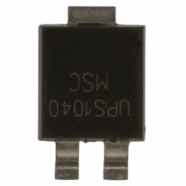


 工商网监
湘ICP备2023018690号
工商网监
湘ICP备2023018690号
