REVISIONS
LTR
DESCRIPTION
DATE (YR-MO-DA)
APPROVED
A
Delete subgroups 10 and 11 in Table IIA for device class Q. - lgt
00-03-07
R. MONNIN
B
Change made to paragraph 3.2.3. Remove radiation test circuit for device
types 01 and 02. – rrp
00-10-13
R. MONNIN
C
Delete case outline Z figure 1. Drawing updated to reflect current
requirements. – gt
03-02-28
R. MONNIN
D
For device type 02 only, make change to IOS(+) and IOS(-) test limits as
specified under Table I. - ro
05-10-24
R. MONNIN
REV
SHEET
REV
D
SHEET
15
REV STATUS
REV
D
D
D
D
D
D
D
D
D
D
D
D
D
D
OF SHEETS
SHEET
1
2
3
4
5
6
7
8
9
10
11
12
13
14
PMIC N/A
PREPARED BY
L.G. TRAYLOR
STANDARD
MICROCIRCUIT
DRAWING
THIS DRAWING IS AVAILABLE
FOR USE BY ALL
DEPARTMENTS
AND AGENCIES OF THE
DEPARTMENT OF DEFENSE
AMSC N/A
DEFENSE SUPPLY CENTER COLUMBUS
COLUMBUS, OHIO 43218-3990
http://www.dscc.dla.mil
CHECKED BY
RAJESH PITHADIA
APPROVED BY
RAY MONNIN
DRAWING APPROVAL DATE
99-02-12
REVISION LEVEL
D
MICROCIRCUIT, LINEAR, RADIATION
HARDENED, SINGLE, LOW-INPUT-CURRENT
OPERATIONAL AMPLIFIER, EXTERNALLY
COMPENSATED, MONOLITHIC SILICON
SIZE
CAGE CODE
A
67268
SHEET
DSCC FORM 2233
APR 97
1 OF
5962-98637
15
5962-E485-05
�1. SCOPE
1.1 Scope. This drawing documents two product assurance class levels consisting of high reliability (device classes Q and M)
and space application (device class V). A choice of case outlines and lead finishes are available and are reflected in the Part or
Identifying Number (PIN). When available, a choice of Radiation Hardness Assurance (RHA) levels is reflected in the PIN.
1.2 PIN. The PIN is as shown in the following example:
5962
R
98637
Federal
stock class
designator
\
RHA
designator
(see 1.2.1)
01
Q
C
A
Device
type
(see 1.2.2)
Device
class
designator
(see 1.2.3)
Case
outline
(see 1.2.4)
Lead
finish
(see 1.2.5)
/
\/
Drawing number
1.2.1 RHA designator. Device classes Q and V RHA marked devices meet the MIL-PRF-38535 specified RHA levels and are
marked with the appropriate RHA designator. Device class M RHA marked devices meet the MIL-PRF-38535, appendix A
specified RHA levels and are marked with the appropriate RHA designator. A dash (-) indicates a non-RHA device.
1.2.2 Device type(s). The device type(s) identify the circuit function as follows:
Device type
01
02
Generic number
Circuit function
PM108A
LM108A
Single low-input-current operational amplifier
Single low-input-current operational amplifier
1.2.3 Device class designator. The device class designator is a single letter identifying the product assurance level as
follows:
Device class
Device requirements documentation
M
Vendor self-certification to the requirements for MIL-STD-883 compliant, nonJAN class level B microcircuits in accordance with MIL-PRF-38535, appendix A
Q or V
Certification and qualification to MIL-PRF-38535
1.2.4 Case outline(s). The case outline(s) are as designated in MIL-STD-1835 and as follows:
Outline letter
Descriptive designator
Terminals
Package style
C
G
H
P
Z
GDIP1-T14 or CDIP2-T14
MACY1-X8
GDFP1-F10 or CDFP2-F10
GDIP1-T8 or CDIP2-T8
GDFP1-G10
14
8
10
8
10
Dual-in-line
Can
Flat pack
Dual-in-line
Flat pack with gull wing leads
1.2.5 Lead finish. The lead finish is as specified in MIL-PRF-38535 for device classes Q and V or MIL-PRF-38535,
appendix A for device class M.
STANDARD
MICROCIRCUIT DRAWING
DEFENSE SUPPLY CENTER COLUMBUS
COLUMBUS, OHIO 43218-3990
DSCC FORM 2234
APR 97
SIZE
5962-98637
A
REVISION LEVEL
D
SHEET
2
�1.3 Absolute maximum ratings. 1/
Supply voltage (VCC) ................................................................................. ± 22 V
Input voltage (VIN) 2/ ................................................................................
Differential input current 3/ .......................................................................
Output short-circuit duration ......................................................................
Storage temperature range ........................................................................
Lead temperature
Device type 01:
(soldering, 60 seconds) ...................................................................
Device type 02:
(soldering, 10 seconds) ...................................................................
Power dissipation (PD) 4/ .........................................................................
Thermal resistance, junction-to-case (θJC) :
Case C, G, H, P ...............................................................................
Case Z ..............................................................................................
Thermal resistance, junction-to-ambient (θJA) : 5/
Device type 01:
Case G .............................................................................................
Case H .............................................................................................
Case P .............................................................................................
Device type 02:
Case C .............................................................................................
Case G .............................................................................................
Case H .............................................................................................
Case P .............................................................................................
Case Z ..............................................................................................
Junction temperature (TJ) ..........................................................................
± 15 V
± 10 mA
Indefinite
-65°C to +150°C
300°C
300°C
500 mW
See MIL-STD-1835
21°C/W
150°C/W
119°C/W
119°C/W
94°C/W
159°C/W
229°C/W
123°C/W
225°C/W
+175°C
1.4 Recommended operating conditions.
Supply voltage (VCC) ................................................................................. ±5 V dc to ±20 V dc
Ambient temperature range (TA) ............................................................... -55°C to +125°C
1.5 Radiation features.
Maximum total dose available (Dose rate = 50 - 300 rads (Si)/s) .............. 100 Krads (Si) 6/
_______
1/ Stresses above the absolute maximum rating may cause permanent damage to the device. Extended operation at the
maximum levels may degrade performance and affect reliability.
2/ For supply voltages less than ±15 V, the absolute maximum input voltage is equal to the supply voltage.
3/ The inputs are shunted with back-to-back diodes for overvoltage protection. Therefore, if a differential input voltage in
excess of 1 V is applied between the inputs, excessive current will flow, unless some limiting resistance is provided.
4/ The maximum power dissipation must be derated at elevated temperatures and is dictated by TJ, θJA, and TA. The
maximum allowable power dissipation at any temperature is PD = (TJ – TA)/θJA or the number in 1.3 herein, whichever is
lower.
5/ θJA is specified for worst case mounting conditions, i.e., θJA is specified for device in socket for TO, CerDIP, and P-DIP
packages.
6/ These parts may be dose rate sensitive in a space environment and may demonstrate enhanced low dose rate effects.
Radiation end point limits for the noted parameters are guaranteed only for the conditions specified in MIL-STD-883, method
1019, condition A.
STANDARD
MICROCIRCUIT DRAWING
DEFENSE SUPPLY CENTER COLUMBUS
COLUMBUS, OHIO 43218-3990
DSCC FORM 2234
APR 97
SIZE
5962-98637
A
REVISION LEVEL
D
SHEET
3
�2. APPLICABLE DOCUMENTS
2.1 Government specification, standards, and handbooks. The following specification, standards, and handbooks form a part
of this drawing to the extent specified herein. Unless otherwise specified, the issues of these documents are those cited in the
solicitation or contract.
DEPARTMENT OF DEFENSE SPECIFICATION
MIL-PRF-38535 - Integrated Circuits, Manufacturing, General Specification for.
DEPARTMENT OF DEFENSE STANDARDS
MIL-STD-883 MIL-STD-1835 -
Test Method Standard Microcircuits.
Interface Standard Electronic Component Case Outlines.
DEPARTMENT OF DEFENSE HANDBOOKS
MIL-HDBK-103 MIL-HDBK-780 -
List of Standard Microcircuit Drawings.
Standard Microcircuit Drawings.
(Copies of these documents are available online at http://assist.daps.dla.mil/quicksearch/ or http://assist.daps.dla.mil or
from the Standardization Document Order Desk, 700 Robbins Avenue, Building 4D, Philadelphia, PA 19111-5094.)
2.2 Order of precedence. In the event of a conflict between the text of this drawing and the references cited herein, the text of
this drawing takes precedence. Nothing in this document, however, supersedes applicable laws and regulations unless a
specific exemption has been obtained.
3. REQUIREMENTS
3.1 Item requirements. The individual item requirements for device classes Q and V shall be in accordance with
MIL-PRF-38535 and as specified herein or as modified in the device manufacturer's Quality Management (QM) plan. The
modification in the QM plan shall not affect the form, fit, or function as described herein. The individual item requirements for
device class M shall be in accordance with MIL-PRF-38535, appendix A for non-JAN class level B devices and as specified
herein.
3.2 Design, construction, and physical dimensions. The design, construction, and physical dimensions shall be as specified in
MIL-PRF-38535 and herein for device classes Q and V or MIL-PRF-38535, appendix A and herein for device class M.
3.2.1 Case outlines. The case outlines shall be in accordance with 1.2.4 herein.
3.2.2 Terminal connections. The terminal connections shall be as specified on figure 1.
3.2.3 Radiation exposure circuit. The radiation exposure circuit shall be maintained by the manufacturer under document
revision level control and shall be made available to the preparing and acquiring activity upon request.
3.3 Electrical performance characteristics and postirradiation parameter limits. Unless otherwise specified herein, the
electrical performance characteristics and postirradiation parameter limits are as specified in table I and shall apply over the full
ambient operating temperature range.
3.4 Electrical test requirements. The electrical test requirements shall be the subgroups specified in table IIA. The electrical
tests for each subgroup are defined in table I.
3.5 Marking. The part shall be marked with the PIN listed in 1.2 herein. In addition, the manufacturer's PIN may also be
marked. For packages where marking of the entire SMD PIN number is not feasible due to space limitations, the manufacturer
has the option of not marking the "5962-" on the device. For RHA product using this option, the RHA designator shall still be
marked. Marking for device classes Q and V shall be in accordance with MIL-PRF-38535. Marking for device class M shall be
in accordance with MIL-PRF-38535, appendix A.
3.5.1 Certification/compliance mark. The certification mark for device classes Q and V shall be a "QML" or "Q" as required in
MIL-PRF-38535. The compliance mark for device class M shall be a "C" as required in MIL-PRF-38535, appendix A.
STANDARD
MICROCIRCUIT DRAWING
DEFENSE SUPPLY CENTER COLUMBUS
COLUMBUS, OHIO 43218-3990
DSCC FORM 2234
APR 97
SIZE
5962-98637
A
REVISION LEVEL
D
SHEET
4
�TABLE I. Electrical performance characteristics.
Test
Symbol
Conditions 1/ 2/ 3/
-55°C ≤ TA ≤+125°C
Group A
subgroups
Device
type
unless otherwise specified
Input offset voltage
VIO
RS = 50 Ω
Min
1
4/
M, D, P, L, R
VCM = -15 V
M, D, P, L, R
VCM = 15 V
M, D, P, L, R
VCM = 0 V
M, D, P, L, R
M, D, P, L, R
∆T
-1.0
1.0
1
-2.0
2.0
-0.5
0.5
2, 3
-1.0
1.0
1
-0.5
0.5
-0.5
0.5
2, 3
-1.0
1.0
1
-0.5
0.5
-0.5
0.5
2, 3
-1.0
1.0
1
-0.5
0.5
-0.5
0.5
2, 3
-1.0
1.0
1
-0.5
0.5
-5.0
5.0
1
+VCC = 5 V, -VCC = -5 V
∆VIO /
2, 3
1
+VCC = 20 V, -VCC = 20 V,
5/ 6/
Max
0.5
1
+VCC = 5 V, -VCC = -35 V,
2, 3
01
Unit
-0.5
1
+VCC = 35 V, -VCC = -5 V,
Input offset voltage
temperature sensitivity
Limits
02
02
02
02
All
mV
mV
mV
mV
mV
µV/°C
See footnotes at end of table.
STANDARD
MICROCIRCUIT DRAWING
DEFENSE SUPPLY CENTER COLUMBUS
COLUMBUS, OHIO 43218-3990
DSCC FORM 2234
APR 97
SIZE
5962-98637
A
REVISION LEVEL
D
SHEET
5
�TABLE I. Electrical performance characteristics - Continued.
Test
Symbol
Conditions 1/ 2/ 3/
-55°C ≤ TA ≤+125°C
Group A
subgroups
Device
type
Limits
unless otherwise specified
Input offset current
IIO
Min
Max
-0.2
0.2
2, 3
-0.4
0.4
M, D, P, L, R
1
-1.0
1.0
+VCC = 35 V, -VCC = -5 V,
1
-0.2
0.2
-0.4
0.4
4/
1
VCM = -15 V, RS = 5 MΩ
1
+VCC = 5 V, -VCC = -35 V,
1
M, D, P, L, R
02
02
+VCC = 5 V, -VCC = -5 V,
M, D, P, L, R
∆IIO/∆T
5/ 6/
0.2
-0.4
0.4
02
-0.2
0.2
-0.4
0.4
1
1
nA
nA
0.5
02
-0.2
0.2
-0.4
0.4
1
2, 3
nA
0.5
2, 3
RS = 5 MΩ
-0.2
1
2, 3
M, D, P, L, R
nA
0.5
2, 3
1
RS = 5 MΩ
01
2, 3
M, D, P, L, R
VCM = 15 V, RS = 5 MΩ
Input offset current
temperature sensitivity
Unit
nA
0.5
All
-2.5
2.5
pA/°C
See footnotes at end of table.
STANDARD
MICROCIRCUIT DRAWING
DEFENSE SUPPLY CENTER COLUMBUS
COLUMBUS, OHIO 43218-3990
DSCC FORM 2234
APR 97
SIZE
5962-98637
A
REVISION LEVEL
D
SHEET
6
�TABLE I. Electrical performance characteristics - Continued.
Test
Conditions 1/ 2/ 3/
-55°C ≤ TA ≤+125°C
Symbol
Group A
subgroups
Device
type
Limits
unless otherwise specified
Input bias current
±IIB
Min
Max
-0.1
2.0
2
-1.0
2.0
3
-0.1
3.0
M, D, P, L, R
1
-25.0
25.0
+VCC = 35 V, -VCC = -5 V,
1
-0.1
2.0
VCM = -15 V, RS = 5 MΩ
2
-1.0
2.0
3
-0.1
3.0
4/
1
M, D, P, L, R
1
+VCC = 5 V, -VCC = -35 V,
1
VCM = 15 V, RS = 5 MΩ
M, D, P, L, R
M, D, P, L, R
+PSRR
-VCC = -20 V,
-PSRR
Input voltage common
mode rejection
CMR
-1.0
2.0
3
-0.1
3.0
02
1
nA
nA
5.0
-0.1
2.0
2
-1.0
2.0
3
-0.1
3.0
02
1
RS = 5 MΩ
nA
5.0
2
1
+VCC = 10 V, RS = 50 Ω,
02
2.0
+VCC = 5 V, -VCC = -5 V,
M, D, P, L, R
01
-0.1
1
RS = 5 MΩ
Power supply
rejection ratio
Unit
nA
5.0
02
-0.1
2.0
2
-1.0
2.0
3
-0.1
3.0
1
nA
5.0
1, 2, 3
All
-16
16
µV/V
1, 2, 3
All
-16
16
µV/V
1, 2, 3
All
96
6/
+VCC = 20 V, RS = 50 Ω,
-VCC = -10 V,
6/
VCM = ±15 V
6/
dB
See footnotes at end of table.
STANDARD
MICROCIRCUIT DRAWING
DEFENSE SUPPLY CENTER COLUMBUS
COLUMBUS, OHIO 43218-3990
DSCC FORM 2234
APR 97
SIZE
5962-98637
A
REVISION LEVEL
D
SHEET
7
�TABLE I. Electrical performance characteristics - Continued.
Test
Symbol
Conditions 1/ 2/ 3/
-55°C ≤ TA ≤+125°C
Group A
subgroups
Device
type
Limits
unless otherwise specified
Adjustment for input
offset voltage
Adjustment for input
offset voltage
Output short-circuit
current (for positive
output)
Output short-circuit
current (for negative
output)
Supply current
VIO
ADJ(+)
VIO
ADJ(-)
IOS(+)
IOS(-)
ICC
Min
Open loop voltage
gain (single ended)
±VOP
1
01
No
external
ADJ
mV
±VCC = ±20 V
6/
1
01
No
external
ADJ
mV
±VCC = ±15 V ,
6/ 7/
1
01
-15.0
mA
02
-20.0
2, 3
02
-20.0
1
01
15.0
02
20.0
2, 3
02
20.0
1, 2
All
0.6
t ≤ 25 ms
±VCC = ±15 V,
6/ 7/
t ≤ 25 ms
±VCC = ±15 V
6/
±VCC = ±20 V,
6/
4, 5, 6
01
-16.0
-16.0
4, 5, 6
02
-VOP
RL = 10 kΩ
4, 5, 6
02
4
01
±VCC = ±15 V,
8/
RL = 10 kΩ, VOUT = ±10 V
M, D, P, L, R
±VCC = ±20 V,
8/
RL = 10 kΩ, VOUT = +15 V
AVS(-)
mA
16.0
V
RL = 10 kΩ
RL = 10 kΩ
AVS(+)
mA
0.8
+VOP
AVS±
Max
6/
±VCC = ±20 V
3
Output voltage swing
(maximum)
Unit
±VCC = ±20 V,
8/
RL = 10 kΩ, VOUT = -15 V
16.0
80
5, 6
40
1
10
4
02
V
V/mV
80
5, 6
4
V
V/mV
40
02
80
V/mV
40
5, 6
See footnotes at end of table.
STANDARD
MICROCIRCUIT DRAWING
DEFENSE SUPPLY CENTER COLUMBUS
COLUMBUS, OHIO 43218-3990
DSCC FORM 2234
APR 97
SIZE
5962-98637
A
REVISION LEVEL
D
SHEET
8
�TABLE I. Electrical performance characteristics - Continued.
Test
Symbol
Conditions 1/ 2/ 3/
-55°C ≤ TA ≤+125°C
Group A
Subgroups
Device
type
Limits
unless otherwise specified
Open loop voltage
gain (single ended)
AVS
Transient response
rise time
TR(tr)
±VCC = ±5 V,
8/
RL = 10 kΩ, VOUT = ±2 V
6/
RL = 10 kΩ, CL = 100 pF,
F < 1 kHz, VIN = +50 mV
Transient response
overshoot
TR(OS)
6/
RL = 10 kΩ, CL = 100 pF,
F < 1 kHz, VIN = +50 mV
SR(+)
Slew rate
VIN = -5 V to +5 V, 6/
Min
Unit
Max
4, 5, 6
02
20
V/mV
9
01
1000
ns
9, 10, 11
02
1000
ns
9
01
50
%
9, 10, 11
02
50
%
9, 10, 11
01
0.05
V/µs
AV = 1
SR(-)
VIN = +5 V to -5 V,
6/
0.05
AV = 1
SR(+)
VIN = -5 V to +5 V,
9, 10, 11
02
0.05
AV = 1
SR(-)
VIN = +5 V to -5 V,
0.05
AV = 1
Noise (referred to
input) broadband
±VCC = ±20 V,
6/
NI(BB)
9
01
15
µV rms
9
02
15
µV rms
BW = 5 kHz, TA = 25°C
BW = 10 Hz to 5 kHz,
NI(BB)
RS = 0 Ω, TA = 25°C
See footnotes at end of table.
STANDARD
MICROCIRCUIT DRAWING
DEFENSE SUPPLY CENTER COLUMBUS
COLUMBUS, OHIO 43218-3990
DSCC FORM 2234
APR 97
SIZE
5962-98637
A
REVISION LEVEL
D
SHEET
9
�TABLE I. Electrical performance characteristics - Continued.
Test
Symbol
Conditions 1/ 2/ 3/
-55°C ≤ TA ≤+125°C
Group A
Subgroups
Device
type
Limits
unless otherwise specified
Noise (referred to
input) popcorn
NI(PC)
±VCC = 20 V,
Min
6/
Unit
Max
9
01
40
µV pk
9
02
40
µV pk
BW = 5 kHz, TA = 25°C
BW = 10 Hz to 5 kHz,
RS = 100 kΩ
1/
Devices supplied to this drawing have been characterized through all levels M, D, P, L, R of irradiation. However, this device
is only tested at the “R” level. Pre and Post irradiation values are identical unless otherwise specified in table I.
2/
These parts may be dose rate sensitive in a space environment and may demonstrate enhanced low dose rate effects.
Radiation end point limits for the noted parameters are guaranteed only for the conditions specified in MIL-STD-883, method
1019, condition A.
3/
Unless otherwise specified test conditions include : VCC = ±20 V, TA = 25°C, RS = 50 Ω, VCM = 0 V.
4/
Tests at common-mode VCM = 0 V, VCM = -15 V, and VCM = +15 V.
5/
Calculated parameters for device type 02.
6/
This parameter not tested post radiation.
7/
Continuous short-circuit limits will be considerably less than the indicated test limits. Continuous IOS at TA ≤ 75°C will cause
TJ to exceed the maximum of 175°C.
8/
Note that gain is not specified at VIO(ADJ) extremes. For closed-loop applications (closed-loop gain less than 1000), the
open-loop tests (AVS) prescribed herein should guarantee a positive, reasonably linear, transfer characteristic. They do not,
however, guarantee that the open-loop gain is linear, or even positive over the operating range. If either of these
requirements exist (positive open-loop gain or open-loop gain linearity), they should be specified in the individual
procurement document as additional requirements.
3.6 Certificate of compliance. For device classes Q and V, a certificate of compliance shall be required from a QML-38535
listed manufacturer in order to supply to the requirements of this drawing (see 6.6.1 herein). For device class M, a certificate of
compliance shall be required from a manufacturer in order to be listed as an approved source of supply in MIL-HDBK-103 (see
6.6.2 herein). The certificate of compliance submitted to DSCC-VA prior to listing as an approved source of supply for this
drawing shall affirm that the manufacturer's product meets, for device classes Q and V, the requirements of MIL-PRF-38535 and
herein or for device class M, the requirements of MIL-PRF-38535, appendix A and herein.
3.7 Certificate of conformance. A certificate of conformance as required for device classes Q and V in MIL-PRF-38535 or for
device class M in MIL-PRF-38535, appendix A shall be provided with each lot of microcircuits delivered to this drawing.
3.8 Notification of change for device class M. For device class M, notification to DSCC-VA of change of product (see 6.2
herein) involving devices acquired to this drawing is required for any change that affects this drawing.
STANDARD
MICROCIRCUIT DRAWING
DEFENSE SUPPLY CENTER COLUMBUS
COLUMBUS, OHIO 43218-3990
DSCC FORM 2234
APR 97
SIZE
5962-98637
A
REVISION LEVEL
D
SHEET
10
�Device types
Case outlines
01, 02
G, P
Terminal number
02
H
C
Z
Terminal symbol
1
COMP
NC
NC
NC
2
-IN
NC
COMP
NC
3
+IN
-IN
NC
-IN
4
V-
+IN
-IN
+IN
5
NC
NC
+IN
NC
6
OUT
V-
NC
V-
7
V+
OUT
V-
OUT
8
COMP
V+
NC
V+
9
---
COMP
NC
COMP
10
---
COMP
OUT
COMP
11
---
---
V+
---
12
---
---
COMP
---
13
---
---
NC
---
14
---
---
NC
---
NC = No connection
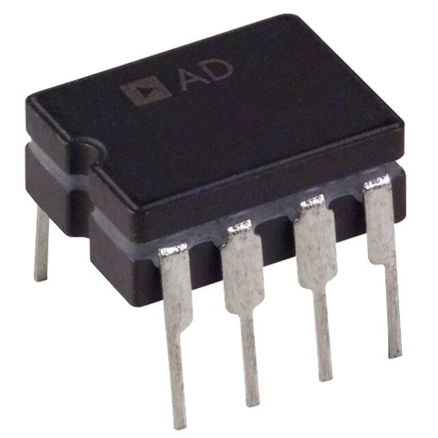
FIGURE 1. Terminal connections.
STANDARD
MICROCIRCUIT DRAWING
DEFENSE SUPPLY CENTER COLUMBUS
COLUMBUS, OHIO 43218-3990
DSCC FORM 2234
APR 97
SIZE
5962-98637
A
REVISION LEVEL
D
SHEET
11
�3.9 Verification and review for device class M. For device class M, DSCC, DSCC's agent, and the acquiring activity retain the
option to review the manufacturer's facility and applicable required documentation. Offshore documentation shall be made
available onshore at the option of the reviewer.
3.10 Microcircuit group assignment for device class M. Device class M devices covered by this drawing shall be in
microcircuit group number 49 (see MIL-PRF-38535, appendix A).
4. VERIFICATION
4.1 Sampling and inspection. For device classes Q and V, sampling and inspection procedures shall be in accordance with
MIL-PRF-38535 or as modified in the device manufacturer's Quality Management (QM) plan. The modification in the QM plan
shall not affect the form, fit, or function as described herein. For device class M, sampling and inspection procedures shall be in
accordance with MIL-PRF-38535, appendix A.
4.2 Screening. For device classes Q and V, screening shall be in accordance with MIL-PRF-38535, and shall be conducted
on all devices prior to qualification and technology conformance inspection. For device class M, screening shall be in
accordance with method 5004 of MIL-STD-883, and shall be conducted on all devices prior to quality conformance inspection.
4.2.1 Additional criteria for device class M.
a.
Burn-in test, method 1015 of MIL-STD-883.
(1) Test condition A, B, C, or D. The test circuit shall be maintained by the manufacturer under document revision
level control and shall be made available to the preparing or acquiring activity upon request. The test circuit shall
specify the inputs, outputs, biases, and power dissipation, as applicable, in accordance with the intent specified in
method 1015.
(2) TA = +125°C, minimum.
b.
Interim and final electrical test parameters shall be as specified in table IIA herein.
4.2.2 Additional criteria for device classes Q and V.
a.
The burn-in test duration, test condition and test temperature, or approved alternatives shall be as specified in the
device manufacturer's QM plan in accordance with MIL-PRF-38535. The burn-in test circuit shall be maintained under
document revision level control of the device manufacturer's Technology Review Board (TRB) in accordance with
MIL-PRF-38535 and shall be made available to the acquiring or preparing activity upon request. The test circuit shall
specify the inputs, outputs, biases, and power dissipation, as applicable, in accordance with the intent specified in
method 1015 of MIL-STD-883.
b.
Interim and final electrical test parameters shall be as specified in table IIA herein.
c.
Additional screening for device class V beyond the requirements of device class Q shall be as specified in
MIL-PRF-38535, appendix B.
4.3 Qualification inspection for device classes Q and V. Qualification inspection for device classes Q and V shall be in
accordance with MIL-PRF-38535. Inspections to be performed shall be those specified in MIL-PRF-38535 and herein for groups
A, B, C, D, and E inspections (see 4.4.1 through 4.4.4).
4.4 Conformance inspection. Technology conformance inspection for classes Q and V shall be in accordance with
MIL-PRF-38535 including groups A, B, C, D, and E inspections and as specified herein. Quality conformance inspection for
device class M shall be in accordance with MIL-PRF-38535, appendix A and as specified herein. Inspections to be performed
for device class M shall be those specified in method 5005 of MIL-STD-883 and herein for groups A, B, C, D, and E inspections
(see 4.4.1 through 4.4.4).
4.4.1 Group A inspection.
a.
Tests shall be as specified in table IIA herein.
b.
Subgroups 7 and 8 in table I, method 5005 of MIL-STD-883 shall be omitted.
STANDARD
MICROCIRCUIT DRAWING
DEFENSE SUPPLY CENTER COLUMBUS
COLUMBUS, OHIO 43218-3990
DSCC FORM 2234
APR 97
SIZE
5962-98637
A
REVISION LEVEL
D
SHEET
12
�TABLE IIA. Electrical test requirements.
Test requirements
Subgroups
(in accordance with
MIL-PRF-38535, table III)
Subgroups
(in accordance with
MIL-STD-883,
method 5005, table I)
Device
class M
Device
class Q
Device
class V
1
1
1
1, 2, 3, 4 1/
1, 2, 3, 4 1/
1, 2, 3, 4
1/ 2/ 3/
Group A test
requirements (see 4.4)
Group C end-point electrical
parameters (see 4.4)
1, 2, 3, 4, 5, 6, 9
1, 2, 3, 4, 5, 6,
9
1, 2, 3, 4, 5,
6, 9, 10, 11
1
1
1, 2, 3
2/ 3/
Group D end-point electrical
parameters (see 4.4)
Group E end-point electrical
parameters (see 4.4)
1
1
1, 2, 3
---
1
1
Interim electrical
parameters (see 4.2)
Final electrical
parameters (see 4.2)
1/ PDA applies to subgroup 1.
2/ Delta limits as specified in table IIB shall be required where specified, and the delta limits
shall be computed with reference to the previous endpoint electrical parameters.
3/ For device type 02 delta is performed for Group C end point electrical only.
Table IIB. 240 hour burn-in and group C end-point electrical parameters.
Test
Device types
Delta
Min
Max
VIO 1/
All
-0.25 mV
+0.25 mV
+IIB 1/
All
-0.5 nA
+0.5 nA
-IIB 1/
All
-0.5 nA
+0.5 nA
1/ VCC = ±20 V, VCM = 0 V.
STANDARD
MICROCIRCUIT DRAWING
DEFENSE SUPPLY CENTER COLUMBUS
COLUMBUS, OHIO 43218-3990
DSCC FORM 2234
APR 97
SIZE
5962-98637
A
REVISION LEVEL
D
SHEET
13
�4.4.2 Group C inspection. The group C inspection end-point electrical parameters shall be as specified in table IIA herein.
4.4.2.1 Additional criteria for device class M. Steady-state life test conditions, method 1005 of MIL-STD-883:
a.
Test condition A, B, C, or D. The test circuit shall be maintained by the manufacturer under document revision level
control and shall be made available to the preparing or acquiring activity upon request. The test circuit shall specify the
inputs, outputs, biases, and power dissipation, as applicable, in accordance with the intent specified in method 1005 of
MIL-STD-883.
b.
TA = +125°C, minimum.
c.
Test duration: 1,000 hours, except as permitted by method 1005 of MIL-STD-883.
4.4.2.2 Additional criteria for device classes Q and V. The steady-state life test duration, test condition and test temperature,
or approved alternatives shall be as specified in the device manufacturer's QM plan in accordance with MIL-PRF-38535. The
test circuit shall be maintained under document revision level control by the device manufacturer's TRB in accordance with
MIL-PRF-38535 and shall be made available to the acquiring or preparing activity upon request. The test circuit shall specify the
inputs, outputs, biases, and power dissipation, as applicable, in accordance with the intent specified in method 1005 of MIL-STD883.
4.4.3 Group D inspection. The group D inspection end-point electrical parameters shall be as specified in table IIA herein.
4.4.4 Group E inspection. Group E inspection is required only for parts intended to be marked as radiation hardness
assured (see 3.5 herein). RHA levels for device classes M, Q, and V shall be as specified in MIL-I-38535. End-point electrical
parameters shall be as specified in table IIA herein.
4.4.4.1 Total dose irradiation testing. Total dose irradiation testing shall be performed in accordance with MIL-STD-883
method 1019 condition A and as specified herein.
4.4.4.1.1 Accelerated aging test. Accelerated aging tests shall be performed on all devices requiring a RHA level greater than
5k rads(SI). The post-anneal end-point electrical parameter limits shall be as specified in table I herein and shall be the preirradiation end-point electrical parameter limit at 25°C ± 5°C. Testing shall be performed at initial qualification and after any
design or process changes which may affect the RHA response of the device.
4.4.4.2 Dose rate burnout. When required by the customer test shall be performed on devices, SEC, or approved test
structures at technology qualifications and after any design or process changes which may effect the RHA capability of the
process. Dose rate burnout shall be performed in accordance with test method 1023 of MIL-STD-883 and as specified herein.
5. PACKAGING
5.1 Packaging requirements. The requirements for packaging shall be in accordance with MIL-PRF-38535 for device classes
Q and V or MIL-PRF-38535, appendix A for device class M.
6. NOTES
6.1 Intended use. Microcircuits conforming to this drawing are intended for use for Government microcircuit applications
(original equipment), design applications, and logistics purposes.
6.1.1 Replaceability. Microcircuits covered by this drawing will replace the same generic device covered by a contractor
prepared specification or drawing.
6.1.2 Substitutability. Device class Q devices will replace device class M devices.
6.2 Configuration control of SMD's. All proposed changes to existing SMD's will be coordinated with the users of record for
the individual documents. This coordination will be accomplished using DD Form 1692, Engineering Change Proposal.
STANDARD
MICROCIRCUIT DRAWING
DEFENSE SUPPLY CENTER COLUMBUS
COLUMBUS, OHIO 43218-3990
DSCC FORM 2234
APR 97
SIZE
5962-98637
A
REVISION LEVEL
D
SHEET
14
�6.3 Record of users. Military and industrial users should inform Defense Supply Center Columbus (DSCC) when a system
application requires configuration control and which SMD's are applicable to that system. DSCC will maintain a record of users
and this list will be used for coordination and distribution of changes to the drawings. Users of drawings covering microelectronic
devices (FSC 5962) should contact DSCC-VA, telephone (614) 692-0544.
6.4 Comments. Comments on this drawing should be directed to DSCC-VA, Columbus, Ohio 43218-3990, or telephone (614)
692-0547.
6.5 Abbreviations, symbols, and definitions. The abbreviations, symbols, and definitions used herein are defined in
MIL-PRF-38535 and MIL-HDBK-1331.
6.6 Sources of supply.
6.6.1 Sources of supply for device classes Q and V. Sources of supply for device classes Q and V are listed in QML-38535.
The vendors listed in QML-38535 have submitted a certificate of compliance (see 3.6 herein) to DSCC-VA and have agreed to
this drawing.
6.6.2 Approved sources of supply for device class M. Approved sources of supply for class M are listed in MIL-HDBK-103.
The vendors listed in MIL-HDBK-103 have agreed to this drawing and a certificate of compliance (see 3.6 herein) has been
submitted to and accepted by DSCC-VA.
STANDARD
MICROCIRCUIT DRAWING
DEFENSE SUPPLY CENTER COLUMBUS
COLUMBUS, OHIO 43218-3990
DSCC FORM 2234
APR 97
SIZE
5962-98637
A
REVISION LEVEL
D
SHEET
15
�STANDARD MICROCIRCUIT DRAWING BULLETIN
DATE: 05-10-24
Approved sources of supply for SMD 5962-98637 are listed below for immediate acquisition information only and shall
be added to MIL-HDBK-103 and QML-38535 during the next revision. MIL-HDBK-103 and QML-38535 will be revised
to include the addition or deletion of sources. The vendors listed below have agreed to this drawing and a certificate
of compliance has been submitted to and accepted by DSCC-VA. This information bulletin is superseded by the next
dated revision of MIL-HDBK-103 and QML-38535. DSCC maintains an online database of all current sources of
supply at http://www.dscc.dla.mil/Programs/Smcr/.
Standard
microcircuit drawing
PIN 1/
Vendor
CAGE
number
Vendor
similar
PIN 2/
5962R9863701VGA
24355
PM108AJ/QMLR
5962R9863701VPA
24355
PM108AZ/QMLR
5962R9863701VHA
24355
PM108AL/QMLR
5962R9863702QCA
27014
LM108AJRQML
5962R9863702QGA
27014
LM108AHRQML
5962R9863702QPA
3/
LM108AJ-8RQML
5962R9863702QHA
27014
LM108AWRQML
5962R9863702QZA
27014
LM108AWGRQML
5962R9863702VCA
27014
LM108AJRQMLV
5962R9863702VGA
27014
LM108AHRQMLV
5962R9863702VPA
27014
LM108AJ-8RQMLV
5962R9863702VHA
27014
LM108AWRQMLV
5962R9863702VZA
27014
LM108AWGRQMLV
1/ The lead finish shown for each PIN representing
a hermetic package is the most readily available
from the manufacturer listed for that part. If the
desired lead finish is not listed contact the vendor
to determine its availability.
2/ Caution. Do not use this number for item
acquisition. Items acquired to this number may not
satisfy the performance requirements of this drawing.
3/ Not available from an approved source of supply.
1 of 2
�STANDARD MICROCIRCUIT DRAWING BULLETIN – CONTINUED.
Vendor CAGE
number
Vendor name
and address
24355
Analog Devices
Route 1 Industrial Park
P.O. Box 9106
Norwood MA 02062
Point of contact : 1500 Space Park Drive
P.O. Box 58020
Santa Clara, CA 95050-8020
27014
National Semiconductor
2900 Semiconductor Dr.
P.O. Box 58090
Santa Clara, CA 95052-8090
The information contained herein is disseminated for convenience only and the
Government assumes no liability whatsoever for any inaccuracies in the
information bulletin.
2 of 2
�