One Technology Way · P.O. Box 9106 · Norwood, MA 02062-9106 · Tel: 781.329.4700 · Fax: 781.461.3113 · www.analog.com
AD8232 EVALUATION BOARD
DOCUMENTATION
FEATURES
●
●
●
●
●
Ready to use Heart Rate Monitor (HRM) Front end
Accepts 2 or 3 electrode options
Directly interface to data acquisition or ADC
Access features with switch jumpers
Allows various circuit configurations
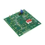
Figure 1.
GENERAL DESCRIPTION
The AD8232-EVALZ contains an AD8232 Heart Rate Monitor Front End conveniently mounted with the
necessary components for initial evaluation in fitness applications. Inputs, outputs, supplies and other
circuit test points have been routed to vector pins to simplify connectivity to test clips and probes.
Switches and jumpers are available for setting the input common-mode, shutdown (SDN), fast-restore
Rev 03 Jan 2013 19:42 | Page 1
�(FR), and AC/DC leads-off detection.
QUICK START
The board ships with a default configuration for three-electrode systems connected to the hands.
Ensure that the switches and jumpers are set to the default values shown in Table 1. For
two-electrode configurations, the settings are shown in Table 2.
TABLE 1. Quick Start Switch Settings
FUNCTION
LABEL CONFIGURATION
Shutdown
P1
Enabled
Fast Restore
P2
Enabled
AC/DC Leads Detection P5
DC method enabled
5V Input
P4
5V input LDO disabled
Input pull-up voltage J2
Pull up inputs to +VS
Note that the 5V LDO may not be installed on all boards
Figure 2. Default Board Settings
1. Connect the power supply common to the GND terminal on the board. Connect a positive supply
voltage between 3V and 3.3V to the +VS terminal.
2. Connect the input electrodes to the +VIN and –VIN terminals.
3. The right-leg drive is available via the RLD terminal. Connect this terminal to the subject with a
third electrode.
4. The output signal is available on the VOUT terminal and it may be connected to a scope or ADC.
Rev 03 Jan 2013 19:42 | Page 2
�Note that the electrode interfaces +VIN, -VIN and RLD are equipped with 180kΩ and 499kΩ (R6,
R7 and R1 respectively) resistors to limit current injection to the subject in the event of fault or
overload. Please note that these will not protect against supply line transients coming through
the system. Isolation from the power line is always required when connecting to a live subject. It
is recommended to fully understand common safety practices; the proper application of such
guidelines is sole responsibility of the end user.
DEFAULT CIRCUIT CONFIGURATION
Signal Path: Inamp and Filters
The evaluation board ships with a default configuration for applications that involve three-electrodes
connected at the hands. The terminals +VIN, –VIN, and RLD serve as the inputs and right-leg drive
electrode connections respectively.
The instrumentation amplifier has a fixed gain of 100 and the op-amp is set for a gain of 11. The
overall gain is 1100V/V, which limits the maximum differential input signal to about 2.7mVp-p.
Exceeding this amplitude will not damage the AD8232, but the signal at the output will appear
distorted. Due to the filter’s high-Q, there is additional peaking that sets the maximum observed gain
above 1100V/V around 15Hz. The total gain may be changed by adjusting the resistors R12 and R13,
but this will have a direct impact on the Q of the low-pass filter. Note that the instrumentation
amplifier has a fixed gain of 100.
A single-supply is used to implement the entire signal chain. For this purpose, the reference buffer is
set to a ratiometric level at mid-supply using two 10MΩ resistors (R8 and R10). The integrated
reference buffer output provides a virtual ground level to allow high-pass filtering. The signal at the
output will ride on top of this mid-supply level. This voltage is available at the REFOUT pin to serve as
a zero level for subsequent signal-acquisition stages.
The circuit implements a two-pole high pass filter for eliminating motion artifacts and the electrode
half-cell potential. Additionally, the integrated operational amplifier creates a two-pole low pass filter
to remove line noise and other interference signals. The frequency cutoff of all filters may be changed
by adjusting component values.
A complete version of the schematic and a section summarizing the explanation of the components
can be found at the end of this document.
Rev 03 Jan 2013 19:42 | Page 3
�Figure 3. AD8232-CHARZ Board Simplified Schematic (Refer to Figure 12 for complete version)
Right-Leg Drive Amplifier
The integrated right-leg drive (RLD) amplifier senses the common mode voltage present at the signal
inputs and can drive an opposing signal into the patient. This driven electrode functionality maintains
the voltage between the patient and the AD8232 constant, greatly improving the common mode
rejection ratio.
The board configures the RLD amplifier as an integrator, formed by an internal 150kΩ resistor and an
external capacitor of 1nF (C1). This results in a loop gain of about 20 at line frequencies, with a
crossover frequency of about 1 kHz.
In a two-lead configuration, the RLD pin can be used to drive the bias current resistors on the inputs.
To create this connection, place a jumper on J3.
Rev 03 Jan 2013 19:42 | Page 4
�FILTER DESIGN
The resistor and capacitor values for the filters were selected to provide effective noise rejection in
applications that involve pulse detection while the subject is in motion. The filter parameters can be
adjusted to fit other applications.
High-Pass Filters
The instrumentation amplifier in the AD8232 applies gain and high pass filtering simultaneously. This
capability allows it to amplify a small ECG signal by 100 while rejecting electrode offsets as large as
±300 mV. The cutoff frequency of this filter is given by the following equation
fc = 100 / (2π R9 C6)
In this particular case, R9= 10MΩ and C6 = 0.22μF place the pole of the first high-pass at 7Hz. Note
that the filter cutoff is 100 times higher than would be typically expected, because of the feedback
architecture of the instrumentation amplifier.
Figure 4. Frequency response In-Amp filter (dc blocking feature)
An ac-coupling network (C9 and R11) at the output of the instrumentation amplifier introduces a
second pole. The cutoff frequency is that of a regular passive first-order high-pass filter
fc = 1 / (2π R11 C9)
This results in a 7Hz cutoff frequency for 0.22μF and 100kΩ. Both high-pass filters together yield a
total roll-off of 40dB per decade. Be aware that setting the same pole location for both high-pass
filters will result in 6dB attenuation at the corner frequency. In addition, because the output of this
filter is unbuffered, the instrumentation amplifier exhibits higher output impedance at the input of the
Rev 03 Jan 2013 19:42 | Page 5
�subsequent low pass filter. The component values selected on the evaluation board yield good results
without the need of a buffer. Keep this in mind when changing component values.
Low-Pass Filter
The internal uncommitted op amp is used to build a two-pole low pass filter with gain, using a
Sallen-Key configuration. The following design equations set the low-pass cut-off frequency, gain and
Q.
fc = 1 / [2π √(R18 C14 R17 C7)]
Gain = 1 + R12/R13
Q = √{ (R17 C14 R18 C7) / [R17 C14 + R18 C14 + R18 C7 (1 - Gain) ] }
Notice that changing the gain or the cutoff frequency will have an effect on Q and vice versa.
The evaluation board components place the cutoff frequency for the low-pass filter at approximately
25Hz and the gain to 11. Keep the sum of R12 and R13 above 50kΩ to save power and to avoid
excessive loading of the output.
Figure 5 shows the transfer function of the signal from the differential input of the instrumentation
amplifier to VOUT with the default filter configuration.
Figure 5. Gain vs. Frequency
Rev 03 Jan 2013 19:42 | Page 6
�Additional Low-Pass Filters
The components R14, C13, R19 and C15 offer additional filtering options. The pin labeled VFILT is
located after the first filter (R14 and C13). The pin labeled VFILT2 is located after both filters.
LEADS-OFF DETECTION
The AD8232 includes leads off detection features. It provides modes optimized for either two or
three-electrode configurations.
DC Leads-Off Detection
To use this mode, the switch position must match the text labeled as “DC” on the silkscreen. This
mode works by sensing when either input goes high. Note that the system must be a three-electrode
configuration to operate properly. Therefore, the RLD output terminal must be connected to a driven
electrode.
In DC leads-off mode, the AD8232 checks each input individually, and is therefore able to indicate
which electrode is disconnected. The AD8232 indicates which electrode is disconnected by setting the
corresponding LO- or LO+ pin high.
AC Leads-Off Detection
To use this mode, the switch position must match the text labeled as “AC” on the silkscreen. To
maintain the inputs inside the common-mode range of the amplifier, provide a bias return path for
each input with a 10MΩ to REFOUT (through J1) or PRLD (through J3).
This mode is useful when using only two electrodes (no separate driven electrode). The AD8232
detects when an electrode is disconnected by sourcing a small 100 kHz current into the electrodes. As
opposed to the DC detection mode, the ADC8232 is only able to determine that an electrode has lost
its connection – not which one. During such event, the LO+ pin goes high. In this mode, the LO- pin is
not used.
FAST RESTORE
The fast restore function (FR) reduces the duration of otherwise long settling tails of the high-pass
filters. After an abrupt change that rails the amplifier (such as a leads-off condition), the AD8232
automatically adjusts to higher filter cutoff. This functionality allows the AD8232 to recover quickly,
Rev 03 Jan 2013 19:42 | Page 7
�and therefore take valid measurements soon after connecting the electrodes to the subject. To access
this function, set the jumper P2 connection between pins 1 and 2. To disable, connect pins 2 and 3.
BOARD SETTINGS FOR TWO ELECTRODE CONFIGURATION
The AD8232-CHAR-Z can be configured to suit two-electrode applications, as shown in Table 2.
TABLE 2. Two-electrode configuration
FUNCTION
LABEL
CONFIGURATION
AC/DC Leads Detection P5
AC method enabled
Input pull-up voltage J3
Pull up inputs to PRLD or place jumper on J1 to connect to VREF
Keep in mind that the gain and filtering may need to be adjusted depending on the location of the
electrodes. Note that narrow bandwidths offer the highest rejection to motion artifacts and other
external interferences, but introduce distortion into the ECG signal.
EVALUATION BOARD COMPONENT EXPLANATION
Input Bias Circuit: R4, R5, J1, J2, J3, J4
In three-electrode configurations, pull-up resistors are necessary for the leads-off functionality to work
correctly. In two-electrode configurations, biasing the inputs within the input range of AD8232 is
necessary for the instrumentation amplifier to work. R4 and R5 are 10 MΩ on the evaluation board.
The resistors may be pulled up to four different values, depending on which jumper is set. Only one
jumper should be connected at a time.
Two-electrode configuration:
J1: Connects pull up resistors to VREF, which is typically at mid-supply.
J3: Connects pull up resistors to the RLD (right-leg drive) amplifier output. This is the recommended
configuration for two electrode configurations
Three-electrode configuration:
J2: Connects pull up resistors to +VS. This is the standard configuration for three-electrode
configurations.
J4: This jumper position allows connecting the pull-up resistors to a voltage provided by the user. This
is useful in systems that expect high power-line noise (50Hz or 60Hz). A higher voltage than the
supply, such as 5V, can help in maintaining the inputs within the common-mode range of the amplifier.
Apply this voltage at the VSETIN pin.
Thoroughly clean the board after performing any solder work around this area, so that residual flux
Rev 03 Jan 2013 19:42 | Page 8
�does not create resistive parasitic paths
In-Amp High Pass Filter: C6, R9
The cutoff frequency is set to 7.2Hz. Refer to the High-Pass Filters section for more information
AC-Coupling: C9, R11
The cutoff frequency of this high-pass filter is set to 7.2Hz. Because this is a DC-blocking circuit,
connecting R11 to the REFOUT voltage is necessary to allow negative signal swings. Refer to the
High-Pass Filters section for more information
Low Pass Filter (Sallen-Key): R12, R13, R17, R18, C7, C14, C11
This circuit provides two functions: a dual pole low pass filter and gain. On the evaluation board, the
cutoff of this filter is set at 25 Hz, and the gain to 11. This brings the total gain of the AD8232 to
11×100 = 1100. Refer to the Low-Pass Filter section for more information
Additional low pass filters: R14, C13, R19, C15
Cutoff frequency for both filters on the evaluation board is 23.4Hz. Refer to the Additional Low-Pass
Filters section for more information
Mid-supply level: R8, R10, C8
R8 and R10 form a ratiometric reference voltage for the system. The AD8232 buffers this voltage and
makes it available at the VREFOUT pin. Select high resistor values for R8 and R10 to reduce power
consumption. The evaluation board uses 10MΩ for both. C8 is required for filtering and stability.
Power line noise will be considerably worse without C8.
The user may bring an external reference level through the VREFSET pin. Removing R8 and R10,
adding series resistance between the external source and VREFTSET, and adjusting C8 may become
necessary if the reference voltage becomes unstable.
Right leg drive: C1, R1
C1 is 1nF, which together with an internal 150kΩ resistor, results in a loop gain of 20 around the
typical line frequencies and a crossover frequency of 1kHz. The value of R1 is set to 499kΩ to avoid
stability problems. For more information, refer to the Right-Leg Drive Amplifier section.
Optional RFI Filter: R6, R7, C3, C4, C5
Pads are provided for capacitors to implement additional RFI filtering. C3 and C5 should be the same
value and well matched. C4 should be a larger value than C3 and C5. This minimizes degradation of
CMRR at higher frequencies due to tolerance mismatch of C3 and C5.
If C3 = C5 = C and R6 = R7 = R then
Common mode signal cutoff frequency: 1/ (2πRC)
Rev 03 Jan 2013 19:42 | Page 9
�Differential signal cutoff frequency: 1/(2πR(2×C4 + C))
Lower common mode signal cutoff frequency will improve RFI rejection, but may increase the risk of
instability with a right leg drive feedback loop
After any solder work in the RFI filter area, the board should be thoroughly cleaned so that residual
flux from the soldering does not create resistive parasitic paths.
EVALUATION BOARD SCHEMATIC
CLICK ON THE PICTURE TO SEE A LARGER VERSION
© Analog Devices, Inc. All rights reserved. Trademarks and
registered trademarks are the property of their respective owners.
Rev 03 Jan 2013 19:42 | Page 10
www.analog.com
�


 工商网监
湘ICP备2023018690号
工商网监
湘ICP备2023018690号

