LF to 2.7 GHz Dual 60 dB TruPwr™ Detector AD8364
FEATURES
RMS measurement of high crest-factor signals Dual-channel and channel difference outputs ports Integrated accurately scaled temperature sensor Wide dynamic range ±1 dB over 60 dB ±0.5 dB temperature-stable linear-in-dB response Low log conformance ripple +5 V operation at 70 mA, –40°C to +85°C Small footprint, 5 mm x 5 mm, LFCSP
FUNCTIONAL BLOCK DIAGRAM
ACOM ACOM
18
COMA
DECA
CHPA
TEMP
VPSR
24
23
22
21
20
19
17
TEMP VPSA 25 INHA 26 INLA 27 PWDN 28 CHANNEL A TruPwr™
VGA CONTROL
ISIG2 ITGT2
CLPA
16 15 14 13 12 11 10 9
VSTA OUTA FBKA OUTP OUTN FBKB OUTB VSTB
APPLICATIONS
Wireless infrastructure power amplifier linearization/control Antenna VSWR monitor Gain and power control and measurement Transmitter signal strength indication (TSSI) Dual-channel wireless infrastructure radios
COMR 29 INLB 30 INHB 31 VPSB
32
OUTA OUTB
CHANNEL B TruPwr™
ISIG2 ITGT2
BIAS
1 2 3
VGA CONTROL
4 5 6 7 8
05334-001
VLVL
CHPB
DECB
Figure 1. Functional Block Diagram
GENERAL DESCRIPTION
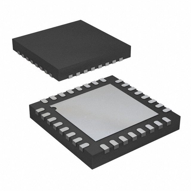
The AD8364 is a true rms, responding, dual-channel RF power measurement subsystem for the precise measurement and control of signal power. The flexibility of the AD8364 allows communications systems, such as RF power amplifiers and radio transceiver AGC circuits, to be monitored and controlled with ease. Operating on a single 5 V supply, each channel is fully specified for operation up to 2.7 GHz over a dynamic range of 60 dB. The AD8364 provides accurately scaled, independent, rms outputs of both RF measurement channels. Difference output ports, which measure the difference between the two channels, are also available. The on-chip channel matching makes the rms channel difference outputs extremely stable with temperature and process variations. The device also includes a useful temperature sensor with an accurately scaled voltage proportional to temperature, specified over the device operating temperature range. The AD8364 can be used with input signals having rms values from −55 dBm to +5 dBm referred to 50 Ω and large crest factors with no accuracy degradation. Integrated in the AD8364 are two matched AD8362 channels (see the AD8362 data sheet for more information) with improved temperature performance and reduced log conformance ripple. Enhancements include improved temperature performance and reduced log-conformance ripple compared to the AD8362. Onchip wide bandwidth output op amps are connected to accommodate flexible configurations that support many system solutions. The device can easily be configured to provide four rms measurements simultaneously. Linear-in-dB rms measurements are supplied at OUTA and OUTB, with conveniently scaled slopes of 50 mV/dB. The rms difference between OUTA and OUTB is available as differential or single-ended signals at OUTP and OUTN. An optional voltage applied to VLVL provides a common mode reference level to offset OUTP and OUTN above ground. The AD8364 is supplied in a 32-lead, 5 mm × 5 mm LFCSP, for the operating temperature of –40°C to +85°C.
Rev. 0
Information furnished by Analog Devices is believed to be accurate and reliable. However, no responsibility is assumed by Analog Devices for its use, nor for any infringements of patents or other rights of third parties that may result from its use. Specifications subject to change without notice. No license is granted by implication or otherwise under any patent or patent rights of Analog Devices. Trademarks and registered trademarks are the property of their respective owners.
One Technology Way, P.O. Box 9106, Norwood, MA 02062-9106, U.S.A. Tel: 781.329.4700 www.analog.com Fax: 781.461.3113 © 2005 Analog Devices, Inc. All rights reserved.
COMB
CLPB
ADJB
ADJA
VREF
�AD8364 TABLE OF CONTENTS
Specifications..................................................................................... 3 Absolute Maximum Ratings............................................................ 7 ESD Caution.................................................................................. 7 Pin Configuration and Function Descriptions............................. 8 Typical Performance Characteristics ............................................. 9 General Description and Theory.................................................. 18 Square Law Detector and Amplitude Target .......................... 19 RF Input Interface ...................................................................... 19 Offset Compensation ................................................................. 19 Temperature Sensor Interface................................................... 20 VREF Interface ........................................................................... 20 Power-Down Interface............................................................... 20 VST[A, B] Interface.................................................................... 20 OUT[A, B, P, N] Outputs .......................................................... 21 Measurement Channel Difference Output Using OUT[P, N] ........................................................................ 22 Controller Mode ......................................................................... 22 RF Measurement Mode Basic Connections............................ 23 Controller Mode Basic Connections ....................................... 24 Constant Output Power Operation.......................................... 27 Gain-Stable Transmitter/Receiver............................................ 29 Temperature Compensation Adjustment................................ 31 Device Calibration and Error Calculation.............................. 31 Selecting Calibration Points to Improve Accuracy over a Reduced Range................................................................ 32 Altering the Slope....................................................................... 34 Channel Isolation ....................................................................... 35 Choosing the Right Value for CHP[A, B] and CLP[A, B].... 36 RF Burst Response Time ........................................................... 36 Single-Ended Input Operation ................................................. 36 Printed Circuit Board Considerations..................................... 37 Package Considerations............................................................. 37 Description of Characterization............................................... 38 Basis for Error Calculations ...................................................... 38 Evaluation and Characterization Circuit Board Layouts...... 40 Evaluation Boards........................................................................... 44 Assembly Drawings.................................................................... 46 Outline Dimensions ....................................................................... 47 Ordering Guide .......................................................................... 47
REVISION HISTORY
4/05—Revision 0: Initial Version
Rev. 0 | Page 2 of 48
�AD8364 SPECIFICATIONS
VS = VPSA = VPSB = VPSR = 5 V, TA = 25°C, Channel A frequency = Channel B frequency, VLVL = VREF, VST[A, B] = OUT[A, B], OUT[P, N] = FBK[A, B], differential input via Balun, CW input f ≤ 2.7 GHz, unless otherwise noted. Table 1.
Parameter OVERALL FUNCTION Signal Input Interface Specified Frequency Range DC Common-Mode Voltage Signal Output Interface Wideband Noise MEASUREMENT MODE, 450 MHz OPERATION ±1 dB Dynamic Range1 ±0.5 dB Dynamic Range1 Maximum Input Level Minimum Input Level Slope Intercept Output Voltage—High Power In Output Voltage—Low Power In Temperature Sensitivity Conditions Channel A and Channel B, CW sine wave input INH[A, B] (Pins 26, 31) INL[A, B] (Pins 27, 30) Min Typ Max Unit
LF 2.5 OUT[A, B] (Pins 15, 10) CLP[A, B] = 0.1µF, fSPOT = 100 kHz, RF input = 2140 MHz, ≥−40 dBm ADJA = ADJB = 0 V, error referred to best fit line using linear regression @ PINH[A, B] = −40 dBm and −20 dBm, TA = 25°C, balun = M/A-Com ETK4-2T Pins OUT[A, B] −40°C < TA < +85°C Pins OUT[A, B], (Channel A/Channel B) −40°C < TA < +85°C, (Channel A/Channel B) ±1 dB error ±1 dB error 40
2.7
GHz V nV/√Hz
Input A to Input B Isolation Input A to OUTB Isolation Input B to OUTA Isolation2
Pins OUT[A, B] @ PINH[A, B] = −10 dBm Pins OUT[A, B] @ PINH[A, B] = −40 dBm Deviation from OUT[A, B] @ 25°C −40°C < TA < 85°C; PINH[A, B] = −10 dBm −40°C < TA < 85°C; PINH[A, B] = −25 dBm −40°C < TA < 85°C; PINH[A, B] = −40 dBm Deviation from OUTP to OUTN @ 25°C −40°C < TA < 85°C; PINH[A, B] = −10 dBm, −25 dBm −40°C < TA < 85°C; PINH[A, B] = −25 dBm, −25 dBm −40°C < TA < 85°C; PINH[A, B] = −40 dBm, −25 dBm Baluns = Macom ETC1.6-4-2-3 (both channels) Freq separation = 1 kHz PINHB = −50 dBm, OUTB = OUTBPINHB ± 1 dB PINHA = −50 dBm, OUTA = OUTAPINHA ± 1 dB INHA/INLA, INHB/INLB differential drive With recommended balun ADJA = ADJB = 0 V, error referred to best fit line using linear regression @ PINH[A, B] = −40 dBm and −20 dBm, TA = 25°C, balun = Mini-Circuits® JTX-4-10T Pins OUT[A, B], (Channel A/Channel B) −40°C < TA < +85°C Pins OUT[A, B], (Channel A/Channel B) −40°C < TA < +85°C ±1 dB error, (Channel A/Channel B) ±1 dB error, (Channel A/Channel B)
69 65 62/59 50/52 12 −58 51.6 −59 2.53 0.99 −0.1, +0.2 −0.2, +0.3 −0.3, +0.4 ±0.25 ±0.2 ±0.2 71 54 54 210||0.1 −12
dB dB dB dB dBm dBm mV/dB dBm V V dB dB dB dB dB dB dB dB dB Ω||pF dB
Input Impedance Input Return Loss MEASUREMENT MODE, 880 MHz OPERATION ±1 dB Dynamic Range1 ±0.5 dB Dynamic Range1 Maximum Input Level Minimum Input Level Slope Intercept Output Voltage—High Power In Output Voltage—Low Power In
Pins OUT[A, B] @ PINH[A, B] = −10 dBm Pins OUT[A, B] @ PINH[A, B] = −40 dBm
Rev. 0 | Page 3 of 48
66/57 58/40 62/54 20/20 8/0 −58/−57 51.6 −59.2 2.54 0.99
dB dB dB dB dBm dBm mV/dB dBm V V
�AD8364
Parameter Temperature Sensitivity Conditions Deviation from OUT[A, B] @ 25°C −40°C < TA < 85°C; PINH[A, B] = −10 dBm −40°C < TA < 85°C; PINH[A, B] = −25 dBm −40°C < TA < 85°C; PINH[A, B] = −40 dBm Deviation from OUTP to OUTN @ 25°C −40°C < TA < 85°C; PINH[A, B] = −10 dBm, −25 dBm −40°C < TA < 85°C; PINH[A, B] = −25 dBm, −25 dBm −40°C < TA < 85°C; PINH[A, B] = −40 dBm, −25 dBm Baluns = Macom ETC1.6-4-2-3 (both channels) PINHB = −50 dBm, OUTB = OUTBPINHB ± 1 dB PINHA = −50 dBm, OUTA = OUTAPINHA ± 1 dB INHA/INLA, INHB/INLB differential drive With recommended balun ADJA = ADJB = 0.75 V, error referred to best fit line using linear regression @ PINH[A, B] = −40 dBm and −20 dBm, TA = 25°C, balun = Murata LDB181G8820C-110 Pins OUT[A, B], (Channel A/Channel B) −40°C < TA < +85°C Pins OUT[A, B], (Channel A/Channel B) −40°C < TA < +85°C ±1 dB error, (Channel A/Channel B) ±1 dB error Min Typ +0.5 +0.5 +0.5 +0.1, −0.2 +0.1, −0.2 +0.1, −0.2 64 35 35 200||0.3 −9 Max Unit dB dB dB dB dB dB dB dB dB Ω||pF dB
Input A to Input B Isolation Input A to OUTB Isolation Input B to OUTA Isolation2 Input Impedance Input Return Loss MEASUREMENT MODE, 1880 MHz OPERATION ±1 dB Dynamic Range1 ±0.5 dB Dynamic Range1 Maximum Input Level Minimum Input Level Slope Intercept Output Voltage—High Power In Output Voltage—Low Power In Temperature Sensitivity
Input A to Input B Isolation Input A to OUTB Isolation Input B to OUTA Isolation2 Input Impedance Input Return Loss MEASUREMENT MODE, 2.14 GHz OPERATION ±1 dB Dynamic Range1 ±0.5 dB Dynamic Range1 Maximum Input Level Minimum Input Level Slope Intercept Output Voltage—High Power In
Pins OUT[A, B] @ PINH[A,B] = −10 dBm Pins OUT[A, B] @ PINH[A,B] = −40 dBm Deviation from OUT[A, B] @ 25°C −40°C < TA < 85°C; PINH[A, B] = −10 dBm −40°C < TA < 85°C; PINH[A, B] = −25 dBm −40°C < TA < 85°C; PINH[A, B] = −40 dBm Deviation from OUTP to OUTN @ 25°C −40°C < TA < 85°C; PINH[A, B] = −10 dBm, −25 dBm −40°C < TA < 85°C; PINH[A, B] = −25 dBm, −25 dBm −40°C < TA < 85°C; PINH[A, B] = −40 dBm, −25 dBm Baluns = Macom ETC1.6-4-2-3 (both channels) PINHB = −50 dBm, OUTB = OUTBPINHB ± 1 dB PINHA = −50 dBm, OUTA = OUTAPINHA ± 1 dB INHA/INLA, INHB/INLB differential drive With recommended balun ADJA = ADJB = 1.02 V, error referred to best fit line using linear regression @ PINH[A, B] = −40 dBm and −20 dBm, TA = 25°C, balun = Murata LDB212G1020C-001 Pins OUT[A, B], (Channel A/Channel B) −40°C < TA < +85°C Pins OUT[A, B], (Channel A/Channel B) −40°C < TA < +85°C ±1 dB Error, (Channel A/Channel B) ±1 dB Error, (Channel A/Channel B) Channel A/Channel B Channel A/Channel B Pins OUT[A, B] @ PINH[A, B] = −10 dBm
Rev. 0 | Page 4 of 48
69/61 60/50 62/51 58/51 11/3 −58 50 −62 2.49 0.98 +0.5, −0.2 +0.5, −0.2 +0.5, −0.2 ±0.3 ±0.3 ±0.3 61 33 33 167||0.14 −8
dB dB dB dB dBm dBm mV/dB dBm V V dB dB dB dB dB dB dB dB dB Ω||pF dB
66/57 58/40 62/54 30/30 −2/−4 −57−51 49.5/52.1 −58.3/−57.1 2.42
dB dB dB dB dBm dBm mV/dB dBm V
�AD8364
Parameter Output Voltage—Low Power In Temperature Sensitivity Conditions Pins OUT[A, B] @ PINH[A, B] = −40 dBm Deviation from OUT[A, B] @ 25°C −40°C < TA < 85°C; PINH[A, B] = −10 dBm −40°C < TA < 85°C; PINH[A, B] = −25 dBm −40°C < TA < 85°C; PINH[A, B] = −40 dBm Deviation from OUTP to OUTN @ 25°C −40°C < TA < 85°C; PINH[A, B] = −10 dBm, −25 dBm −40°C < TA < 85°C; PINH[A, B] = −25 dBm, −25 dBm −40°C < TA < 85°C; PINH[A, B] = −40 dBm, −25 dBm 5.5 dB peak-to-rms ratio (WCDMA one channel) 12 dB peak-to-rms ratio (WCDMA three channels) 18 dB peak-to-rms ratio (WCDMA four channels) Baluns = Macom ETC1.6-4-2-3 (both channels) PINHB = −50 dBm, OUTB = OUTBPINHB ± 1 dB PINHA = −50 dBm, OUTA = OUTAPINHA ± 1 dB INHA/INLA, INHB/INLB differential drive With recommended balun ADJA = ADJB = 1.14 V, error referred to best fit line using linear regression @ PINH[A, B] = −40 dBm and −20 dBm, TA = 25°C, balun = Murata LDB182G4520C-110 Pins OUT[A, B], (Channel A/Channel B) −40°C < TA < +85°C Pins OUT[A, B], (Channel A/Channel B) −40°C < TA < +85°C ±1 dB error, (Channel A/Channel B) ±1 dB error Min Typ 0.90 +0.1, −0.4 +0.1, −0.4 +0.1, −0.4 +0.1, −0.4 +0.2, −0.2 +0.1, −0.2 0.2 0.3 0.3 58 33 33 150||1.9 −10 Max Unit V dB dB dB dB dB dB dB dB dB dB dB dB Ω||pF dB
Deviation from CW Response
Input A to Input B Isolation Input A to OUTB Isolation Input B to OUTA Isolation2 Input Impedance Input Return Loss MEASUREMENT MODE, 2.5 GHz OPERATION ± 1 dB Dynamic Range1 ±0.5 dB Dynamic Range1 Maximum Input Level Minimum Input Level Slope Intercept Output Voltage—High Power In Output Voltage—Low Power In Temperature Sensitivity
Input A to Input B Isolation Input A to OUTB Isolation Input B to OUTA Isolation2 Input Impedance Input Return Loss OUTPUT INTERFACE Voltage Range Min Voltage Range Max Source/Sink Current
Pins OUT[A, B] @ PINH[A, B] = −10 dBm Pins OUT[A, B] @ PINH[A, B] = −40 dBm Deviation from OUT[A, B] @ 25°C −40°C < TA < 85°C; PINH[A, B] = −10 dBm −40°C < TA < 85°C; PINH[A, B] = −25 dBm −40°C < TA < 85°C; PINH[A, B] = −40 dBm Deviation from OUTP to OUTN @ 25°C −40°C < TA < 85°C; PINH[A, B] = −10 dBm, −25 dBm −40°C < TA < 85°C; PINH[A, B] = −25 dBm, −25 dBm −40°C < TA < 85°C; PINH[A, B] = −40 dBm, −25 dBm Baluns = Macom ETC1.6-4-2-3 (both channels) PINHB = −50 dBm, OUTB = OUTBPINHB ± 1 dB PINHA = −50 dBm, OUTA = OUTAPINHA ± 1 dB INHA/INLA, INHB/INLB differential drive With recommended balun Pin OUTA and OUTB RL ≥ 200 Ω to ground RL ≥ 200 Ω to ground OUTA and OUTB held at VS/2, to 1% change
69/63 58 55/50 25 17/11 −52 50 −52.7 2.14 0.65 ±0.5 ±0.5 ±0.5 ±0.3 ±0.3 ±0.3 54 31 31 150||1.7 −11.5 0.09 VS − 0.15 70
dB dB dB dB dBm dBm mV/dB dBm V V dB dB dB dB dB dB dB dB Ω||pF dB V V mA
Rev. 0 | Page 5 of 48
�AD8364
Parameter SETPOINT INPUT Voltage Range Input Resistance Logarithmic Scale Factor Logarithmic Intercept CHANNEL DIFFERENCE OUTPUT Voltage Range Min Voltage Range Max Source/Sink Current DIFFERENCE LEVEL ADJUST Voltage Range3 OUT[P,N] Voltage Range Input Resistance TEMPERATURE COMPENSATION Input Voltage Range Input Resistance VOLTAGE REFERENCE Output Voltage Temperature Sensitivity Current Limit Source/Sink TEMPERATURE REFERENCE Output Voltage Temperature Coefficient Current Source/Sink POWER-DOWN INTERFACE Logic Level to Enable Logic Level to Disable Input Current Enable Time Disable Time POWER INTERFACE Supply Voltage Quiescent Current Supply Current Conditions Pin VSTA and VSTB Law conformance error ≤1 dB f = 450 MHz, −40°C ≤ TA ≤ +85°C f = 450 MHz, −40°C ≤ TA ≤ +85°C, referred to 50 Ω Pin OUTP and OUTN RL ≥ 200 Ω to ground RL ≥ 200 Ω to ground OUTP and OUTN held at VS/2, to 1% change Pin VLVL OUT[P, N] = FBK[A, B] OUT[P, N] = FBK[A, B] Min 0.5 68 50 −55 0.1 VS − 0.15 70 0 0 1 Pin ADJA and ADJB 0 >1 Pin VREF RF in = −55 dBm −40°C ≤ TA ≤ +85°C 1% change Pin TEMP TA = 25°C, RL ≥ 10 kΩ −40°C ≤ TA ≤ +85°C, RL ≥ 10 kΩ TA = 25°C to 1% change Pin PWDN Logic LO enables Logic HI disables Logic HI PWDN = 5 V Logic LO PWDN = 0 V PWDN LO to OUTA/OUTB at 100% final value, CLPA/B = Open, CHPA/B = 10 nF, RF in = 0 dBm PWDN HI to OUTA/OUTB at 10% final value, CLPA/B = Open, CHPA/B = 10nF, RF in = 0 dBm Pin VPS[A, B], VPSR RF in = −55 dBm, VS = 5 V −40°C ≤ TA ≤ +85°C PWDN enabled, VS = 5 V −40°C ≤ TA ≤ +85°C 2.5 0.4 10/3 0.62 2 1.6/2 1 3 95