Quad/Octal Input Network Clock
Generator/Synchronizer
AD9548
Data Sheet
FEATURES
APPLICATIONS
Supports Stratum 2 stability in holdover mode
Supports reference switchover with phase build-out
Supports hitless reference switchover
Auto/manual holdover and reference switchover
4 pairs of reference input pins with each pair configurable as
a single differential input or as 2 independent singleended inputs
Input reference frequencies from 1 Hz to 750 MHz
Reference validation and frequency monitoring (1 ppm)
Programmable input reference switchover priority
30-bit programmable input reference divider
4 pairs of clock output pins with each pair configurable as a
single differential LVDS/LVPECL output or as 2 singleended CMOS outputs
Output frequencies up to 450 MHz
30-bit integer and 10-bit fractional programmable feedback
divider
Programmable digital loop filter covering loop bandwidths
from 0.001 Hz to 100 kHz
Optional low noise LC-VCO system clock multiplier
Optional crystal resonator for system clock input
On-chip EEPROM to store multiple power-up profiles
Software controlled power-down
88-lead LFCSP package
Network synchronization
Cleanup of reference clock jitter
GPS 1 pulse per second synchronization
SONET/SDH clocks up to OC-192, including FEC
Stratum 2 holdover, jitter cleanup, and phase transient
control
Stratum 3E and Stratum 3 reference clocks
Wireless base station controllers
Cable infrastructure
Data communications
GENERAL DESCRIPTION
The AD9548 provides synchronization for many systems,
including synchronous optical networks (SONET/SDH). The
AD9548 generates an output clock synchronized to one of up to
four differential or eight single-ended external input references.
The digital PLL allows for reduction of input time jitter or phase
noise associated with the external references. The AD9548
continuously generates a clean (low jitter), valid output clock
even when all references have failed by means of a digitally
controlled loop and holdover circuitry.
The AD9548 operates over an industrial temperature range of
−40°C to +85°C.
FUNCTIONAL BLOCK DIAGRAM
ANALOG
FILTER
STABLE
SOURCE
AD9548
CLOCK DISTRIBUTION
CLOCK
MULTIPLIER
CHANNEL 0
DIVIDER
CHANNEL 1
DIVIDER
DIGITAL
PLL
CHANNEL 2
DIVIDER
DAC
REFERENCE INPUTS
AND
MONITOR MUX
CHANNEL 3
DIVIDER
SYNC
EEPROM
STATUS AND
CONTROL PINS
08022-001
SERIAL CONTROL INTERFACE
(SPI or I2C)
Figure 1.
Rev. G
Document Feedback
Information furnished by Analog Devices is believed to be accurate and reliable. However, no
responsibility is assumed by Analog Devices for its use, nor for any infringements of patents or other
rights of third parties that may result from its use. Specifications subject to change without notice. No
license is granted by implication or otherwise under any patent or patent rights of Analog Devices.
Trademarks and registered trademarks are the property of their respective owners.
One Technology Way, P.O. Box 9106, Norwood, MA 02062-9106, U.S.A.
Tel: 781.329.4700 ©2009–2014 Analog Devices, Inc. All rights reserved.
Technical Support
www.analog.com
�AD9548
Data Sheet
TABLE OF CONTENTS
Features .............................................................................................. 1
Digital PLL (DPLL) Core .......................................................... 32
Applications ....................................................................................... 1
Direct Digital Synthesizer ......................................................... 34
General Description ......................................................................... 1
Tuning Word Processing ........................................................... 35
Functional Block Diagram .............................................................. 1
Loop Control State Machine ..................................................... 36
Revision History ............................................................................... 3
System Clock Inputs................................................................... 37
Specifications..................................................................................... 4
SYSCLK PLL Multiplier............................................................. 38
Supply Voltage ............................................................................... 4
Clock Distribution ..................................................................... 40
Supply Current .............................................................................. 4
Status and Control .......................................................................... 44
Power Dissipation ......................................................................... 4
Multifunction Pins (M0 to M7) ............................................... 44
Logic Inputs (M7 to M0, RESET, TDI, TCLK, TMS) .............. 5
IRQ Pin ........................................................................................ 45
Logic Outputs (M7 to M0, IRQ, TDO) ..................................... 5
Watchdog Timer ......................................................................... 46
System Clock Inputs (SYSCLKP/SYSCLKN) ........................... 5
EEPROM ..................................................................................... 46
Distribution Clock Inputs (CLKINP/CLKINN) ...................... 6
Serial Control Port ......................................................................... 51
Reference Inputs (REFA/REFAA to REFD/REFDD) .............. 7
SPI/I2C Port Selection................................................................ 51
Reference Monitors ...................................................................... 7
SPI Serial Port Operation .......................................................... 51
Reference Switchover Specifications .......................................... 8
I2C Serial Port Operation .......................................................... 56
Distribution Clock Outputs (OUT0 to OUT3) ........................ 8
Input/Output Programming Registers ........................................ 59
DAC Output Characteristics (DACOUTP/DACOUTN) ....... 9
Buffered/Active Registers .......................................................... 59
Time Duration of Digital Functions ........................................ 10
Autoclear Registers ...................................................................... 59
Digital PLL .................................................................................. 10
Register Access Restrictions ........................................................ 59
Digital PLL Lock Detection ...................................................... 10
Register Map ................................................................................... 60
Holdover Specifications ............................................................. 10
Register Map Bit Descriptions ...................................................... 70
Serial Port Specifications—SPI Mode ...................................... 11
Serial Port Specifications—I C Mode ...................................... 11
Serial Port Configuration (Register 0x0000 to
Register 0x0005) ......................................................................... 70
Jitter Generation ......................................................................... 12
System Clock (Register 0x0100 to Register 0x0108) ............. 71
Absolute Maximum Ratings.......................................................... 14
General Configuration (Register 0x0200 to Register 0x0214) .. 72
ESD Caution ................................................................................ 14
DPLL Configuration (Register 0x0300 to Register 0x031B) 75
Pin Configuration and Function Descriptions ........................... 15
Clock Distribution Output Configuration (Register 0x0400 to
Register 0x0419)........................................................................... 77
2
Typical Performance Characteristics ........................................... 18
Input/Output Termination Recommendations .......................... 23
Reference Input Configuration (Register 0x0500 to
Register 0x0507) ......................................................................... 81
Getting Started ................................................................................ 24
Profile Registers (Register 0x0600 to Register 0x07FF) ........ 83
Power-On Reset .......................................................................... 24
Operational Controls (Register 0x0A00 to Register 0x0A10) ... 92
Initial M0 to M7 Pin Programming ......................................... 24
Clock Part Serial ID (Register 0x0C00 to Register 0x0C07) 97
Device Register Programming .................................................. 24
Status Readback (Register 0x0D00 to Register 0x0D19) ...... 97
Theory of Operation ...................................................................... 26
Overview...................................................................................... 26
Reference Clock Inputs .............................................................. 27
Nonvolatile Memory (EEPROM) Control (Register 0x0E00 to
Register 0x0E03) ........................................................................ 101
Reference Monitors .................................................................... 27
EEPROM Storage Sequence (Register 0x0E10 to
Register 0x0E3F) ........................................................................ 101
Reference Profiles ....................................................................... 28
Power Supply Partitions............................................................... 106
Reference Switchover ................................................................. 30
3.3 V Supplies............................................................................ 106
Rev. G | Page 2 of 111
�Data Sheet
AD9548
1.8 V Supplies ........................................................................... 106
Calculation of the Register Values .......................................110
Thermal Performance .................................................................. 107
Calculation of the Register Values .......................................110
Calculating Digital Filter Coefficients ....................................... 108
Outline Dimensions ......................................................................111
Calculation of the Register Values ..................................... 109
Ordering Guide .........................................................................111
Calculation of the β Register Values ...................................... 109
REVISION HISTORY
12/14—Rev. F to Rev. G
Changes to Figure 7 Caption to Figure 12 Caption ....................19
Changes to System Clock Period Section ....................................39
Changes to Table 36 ........................................................................62
6/14—Rev. E to Rev. F
Changes to Table 21 ........................................................................15
Added Figure 34; Renumbered Sequentially ...............................23
Changed Initial Pin Programming Section to Initial M0 to M7
Pin Programming Section ..............................................................24
Changes to Frequency Tuning Word History Section ...............36
Added Disabling Accidental Automatic EEPROM Download
Section ..............................................................................................48
Changes to Buffered/Active Registers Section ............................59
Changes to Register Map Section, Opt Column, Table 36 ........60
Changes to Table 65 ........................................................................76
12/13—Rev. D to Rev. E
Changes to Calculating Digital Filter Coefficients Section .....109
Changes to Calculation of the Register Values Section ........110
6/13—Rev. C to Rev. D
Change to Table 16 ..........................................................................10
Changes to IRQ Pin Section ..........................................................46
Changes to Programming the EEPROM to Include a Clock
Part ID Section ................................................................................50
Changes to Bit 0, Table 121 ............................................................94
Changes to Status Readback (Register 0x0D00 to Register
0x0D19) Section ..............................................................................98
2/13—Rev. B to Rev. C
Change to Pin 53, Description Column, Table 21 ......................17
Added Figure 33, Renumbered Sequentially ...............................23
Changes to Automatic Priority-Based Reference Switchover
Section; Added Table 23, Renumbered Sequentially ......................30
Changes to Low Loop Bandwidth Applications Using a
TCXO/OCXO Section ....................................................................37
Changes to EEPROM Upload Section and EEPROM
Download Section ...........................................................................48
Added Programming the EEPROM to Include a Clock
Part ID Section ................................................................................50
Changes to Read Section ................................................................ 52
Added Figure 56 .............................................................................. 54
Changes to tC Parameter, Description Column, Table 33 .......... 55
Added Table Summary Statement, Table 36 ................................ 60
Changes to Table 36 ........................................................................ 60
Added User Scratch Pad (Eight Bytes), Address 0x0C00 to
Address 0x0C07, Table 36 .............................................................. 67
Changes to Table 39 ........................................................................ 70
Added Clock Part Serial ID (Register 0x0C00 to
Register 0x0C07) Section and Table 131 ...................................... 98
Changes to Table 142 .................................................................... 102
Added Table 153 ............................................................................ 105
Added Table 154 ............................................................................ 106
7/11—Rev. A to Rev. B
Changed AD9584 to AD9548........................................................ 32
Changed 437,749,988,378,041 to 43,774,988,378,041 ................ 34
Change to Calculating Digital Filter Coefficients Section....... 107
10/10—Rev. 0 to Rev. A
Changes to Timing Parameter, Table 17 ...................................... 11
Added Low Loop Bandwidth Applications Using a TCXO/OCXO
Section and Choosing a System Clock Oscillator Frequency
Section .............................................................................................. 37
Moved System Clock Period Section ............................................ 39
Changes to Addr 0002, Table 35.................................................... 60
Changes to Addr 0600, Table 35.................................................... 62
Changes to Addr 0632, Table 35.................................................... 63
Changes to Addr 0680, Table 35.................................................... 64
Changes to Addr 06B2, Table 35 ................................................... 65
Changes to Address 0002 Description, Table 38 ......................... 70
Changes to Bit 7 and Bit 6, Table 78 ............................................. 83
Changes to Address 0629 and Address 062A, Table 87 and Bit 7
and Bit 6, Table 88 ........................................................................... 85
Changes to Address 065B and Address 065C, Table 97 and Bit 7
and Bit 6, Table 98 ........................................................................... 87
Changes to Address 06A9 and Address 06AA, Table 107 ......... 89
Changes to Bit 7 and Bit 6, Table 108 ........................................... 90
Changes to Address 06DB and Address 06DC, Table 117......... 92
4/09—Revision 0: Initial Version
Rev. G | Page 3 of 111
�AD9548
Data Sheet
SPECIFICATIONS
Minimum (min) and maximum (max) values apply for the full range of supply voltage and operating temperature variations. Typical (typ)
values apply for AVDD3 = DVDD_I/O = 3.3 V; AVDD = DVDD = 1.8 V; TA= 25°C; IDAC = 20 mA (full scale), unless otherwise noted.
SUPPLY VOLTAGE
Table 1.
Parameter
SUPPLY VOLTAGE
DVDD3
DVDD
AVDD3
3.3 V Supply (Typical)
1.8 V Supply (Alternative)
AVDD
Min
Typ
Max
Unit
Test Conditions/Comments
3.135
1.71
3.135
3.135
1.71
1.71
3.30
1.80
3.30
3.30
1.80
1.80
3.465
1.89
3.465
3.465
1.89
1.89
V
V
V
V
V
V
Pin 7, Pin 82
Pin 1, Pin 6, Pin 12, Pin 14, Pin 15, Pin 77, Pin 83, Pin 88
Pin 21, Pin 22, Pin 47, Pin 60, Pin 66, Pin 67, Pin 73
Pin 31, Pin 37, Pin 38, Pin 44
Pin 31, Pin 37, Pin 38, Pin 44
Pin 23, Pin 24, Pin 29, Pin 34, Pin 41, Pin 50, Pin 55, Pin 59,
Pin 63, Pin 70, Pin 74
SUPPLY CURRENT
The test conditions for the maximum (max) supply current are the same as the test conditions for the All Blocks Running parameter of Table 3.
The test conditions for the typical (typ) supply current are the same as the test conditions for the Typical Configuration parameter of Table 3.
Table 2.
Parameter
SUPPLY CURRENT
IDVDD3
IDVDD
IAVDD3
IAVDD3
3.3 V Supply (Typical)
1.8 V Supply (Alternative)
IAVDD
Min
Typ
Max
Unit
Test Conditions/Comments
1.5
190
52
3
215
75
mA
mA
mA
Pin 7, Pin 82
Pin 1, Pin 6, Pin 12, Pin 14, Pin 15, Pin 77, Pin 83, Pin 88
Pin 21, Pin 22, Pin 47, Pin 60, Pin 66, Pin 67, Pin 73
24
24
135
110
110
163
mA
mA
mA
Pin 31, Pin 37, Pin 38, Pin 44
Pin 31, Pin 37, Pin 38, Pin 44
Pin 23, Pin 24, Pin 29, Pin 34, Pin 41, Pin 50, Pin 55, Pin 59,
Pin 63, Pin 70, Pin 74
Typ
Max
Unit
Test Conditions/Comments
800
1100
mW
All Blocks Running
900
1400
mW
Full Power-Down
13
fSYSCLK = 20 MHz1; fS = 1 GHz2; fDDS = 122.88 MHz3; one
LVPECL clock distribution output running at 122.88 MHz
(all others powered down); one input reference running
at 100 MHz (all others powered down)
fSYSCLK = 20 MHz1; fS = 1 GHz2; fDDS = 399 MHz3; all clock
distribution outputs configured as LVPECL at 399 MHz; all
input references configured as differential at 100 MHz;
fractional-N active (R = 10, S = 39, U = 9, V = 10)
Conditions = typical configuration; no external pull-up or
pull-down resistors
POWER DISSIPATION
Table 3.
Parameter
POWER DISSIPATION
Typical Configuration
Min
mW
Rev. G | Page 4 of 111
�Data Sheet
Parameter
Incremental Power Dissipation
AD9548
Min
Typ
SYSCLK PLL Off
Input Reference On
Differential
Single-Ended
Output Distribution Driver On
LVDS
LVPECL
CMOS
Max
Unit
−105
mW
7
13
mW
mW
70
75
65
mW
mW
mW
Test Conditions/Comments
Conditions = typical configuration; table values show the
change in power due to the indicated operation.
fSYSCLK = 1 GHz1; high frequency direct input mode.
A single 3.3 V CMOS output with a 10 pF load.
fSYSCLK is the frequency at the SYSCLKP and SYSCLKN pins.
fS is the sample rate of the output DAC.
3
fDDS is the output frequency of the DDS.
1
2
LOGIC INPUTS (M7 TO M0, RESET, TDI, TCLK, TMS)
Table 4.
Parameter
LOGIC INPUTS (M7 to M0, RESET, TDI, TCLK, TMS)
Input High Voltage (VIH)
Input Low Voltage (VIL)
Input Current (IINH, IINL)
Input Capacitance (CIN)
Min
Typ
Max
Unit
0.8
±200
V
V
µA
pF
Max
Unit
Test Conditions/Comments
0.4
V
V
1
1
μA
μA
IOH = 1 mA
IOL = 1 mA
Open-drain mode
VOH = 3.3 V
VOL =-0 V
2.1
±80
3
Test Conditions/Comments
LOGIC OUTPUTS (M7 TO M0, IRQ, TDO)
Table 5.
Parameter
LOGIC OUTPUTS (M7 to M0, IRQ, TDO)
Output High Voltage (VOH)
Output Low Voltage (VOL)
IRQ Leakage Current
Active Low Output Mode
Active High Output Mode
Min
Typ
2.7
SYSTEM CLOCK INPUTS (SYSCLKP/SYSCLKN)
Table 6.
Parameter
SYSTEM CLOCK PLL BYPASSED
Input Frequency Range
Minimum Input Slew Rate
Duty Cycle
Common-Mode Voltage
Differential Input Voltage Sensitivity
Input Capacitance
Input Resistance
Min
Typ
500
1000
40
Max
Unit
1000
MHz
V/μs
1.2
60
%
V
mV p-p
2
2.5
pF
kΩ
100
Rev. G | Page 5 of 111
Test Conditions/Comments
Minimum limit imposed for jitter
performance
Internally generated
Minimum voltage across pins required to
ensure switching between logic states;
the instantaneous voltage on either pin
must not exceed the supply rails; can
accommodate single-ended input by ac
grounding unused input
Single-ended, each pin
�AD9548
Parameter
SYSTEM CLOCK PLL ENABLED
PLL Output Frequency Range
Phase-Frequency Detector (PFD) Rate
Frequency Multiplication Range
VCO Gain
High Frequency Path
Input Frequency Range
Minimum Input Slew Rate
Frequency Divider Range
Common-Mode Voltage
Differential Input Voltage Sensitivity
Input Capacitance
Input Resistance
Low Frequency Path
Input Frequency Range
Minimum Input Slew Rate
Common-Mode Voltage
Differential Input Voltage Sensitivity
Input Capacitance
Input Resistance
Crystal Resonator Path
Crystal Resonator Frequency Range
Maximum Crystal Motional Resistance
Data Sheet
Min
Typ
900
6
Max
Unit
1000
150
255
MHz
MHz
Test Conditions/Comments
Assumes valid system clock and PFD rates
70
MHz/V
100.1
200
500
1
MHz
V/μs
8
1
V
mV p-p
3
2.5
pF
kΩ
100
3.5
50
100
MHz
V/μs
1.2
V
mV p-p
3
4
pF
kΩ
100
10
50
100
MHz
Ω
Minimum limit imposed for jitter
performance
Binary steps (M = 1, 2, 4, 8)
Internally generated
Minimum voltage across pins required to
ensure switching between logic states;
the instantaneous voltage on either pin
must not exceed the supply rails; can
accommodate single-ended input by ac
grounding unused input
Single-ended, each pin
Minimum limit imposed for jitter
performance
Internally generated
Minimum voltage across pins required to
ensure switching between logic states;
the instantaneous voltage on either pin
must not exceed the supply rails; can
accommodate single-ended input by ac
grounding unused input
Single-ended, each pin
Fundamental mode, AT cut
See the System Clock Inputs section for
recommendations
DISTRIBUTION CLOCK INPUTS (CLKINP/CLKINN)
Table 7.
Parameter
DISTRIBUTION CLOCK INPUTS (CLKINP/CLKINN)
Input Frequency Range
Minimum Slew Rate
Min
Typ
62.5
75
Max
Unit
500
MHz
V/μs
Common-Mode Voltage
Differential Input Voltage Sensitivity
100
mV
mV p-p
Differential Input Power Sensitivity
−15
dBm
Input Capacitance
Input Resistance
700
3
5
Rev. G | Page 6 of 111
pF
kΩ
Test Conditions/Comments
Minimum limit imposed for jitter
performance.
Internally generated.
Capacitive coupling required; can
accommodate single-ended input
by ac grounding unused input; the
instantaneous voltage on either pin
must not exceed the supply rails.
The same as voltage sensitivity but
specified as power into a 50 Ω load.
Each pin has a 2.5 kΩ internal dcbias resistance.
�Data Sheet
AD9548
REFERENCE INPUTS (REFA/REFAA TO REFD/REFDD)
Table 8.
Parameter
DIFFERENTIAL OPERATION
Frequency Range
Sinusoidal Input
LVPECL Input
LVDS Input
Minimum Input Slew Rate
Min
Typ
10
1
1
40
Max
Unit
750
750 × 106
750 × 106
MHz
Hz
Hz
V/μs
Common-Mode Input Voltage
Differential Input Voltage Sensitivity
2
±65
V
mV
Input Resistance
Input Capacitance
25
3
kΩ
pF
Minimum Pulse Width High
Minimum Pulse Width Low
SINGLE-ENDED OPERATION
Frequency Range (CMOS)
Minimum Input Slew Rate
620
620
Minimum limit imposed for jitter
performance
Internally generated
Minimum differential voltage across
pins required to ensure switching
between logic levels; the
instantaneous voltage on either pin
must not exceed the supply rails
ps
ps
1
40
Input Voltage High (VIH)
1.2 V to 1.5 V Threshold Setting
1.8 V to 2.5 V Threshold Setting
3.0 V to 3.3 V Threshold Setting
Input Voltage Low (VIL)
1.2 V to 1.5 V Threshold Setting
1.8 V to 2.5 V Threshold Setting
3.0 V to 3.3 V Threshold Setting
Input Resistance
Input Capacitance
Minimum Pulse Width High
Minimum Pulse Width Low
Test Conditions/Comments
250 ×106
0.9
1.2
1.9
Hz
V/μs
Minimum limit imposed for jitter
performance
V
V
V
0.27
0.5
1.0
V
V
V
kΩ
pF
ns
ns
45
3
1.5
1.5
REFERENCE MONITORS
Table 9.
Parameter
REFERENCE MONITORS
Reference Monitor
Loss of Reference Detection
Time
Frequency Out-of Range Limits
Validation Timer
Redetect Timer
1
Min
9.54 × 10⁻⁷
0.001
0.001
Typ
Max
Unit
Test Conditions/Comments
1.2
sec
0.1
65.535
65.535
Δf/fREF
sec
sec
Calculated using the nominal phase detector period
(NPDP = R/fREF)1
Programmable (lower bound subject to quality of SYSCLK)
Programmable in 1 ms increments
Programmable in 1 ms increments
fREF is the frequency of the active reference; R is the frequency division factor determined by the R-divider.
Rev. G | Page 7 of 111
�AD9548
Data Sheet
REFERENCE SWITCHOVER SPECIFICATIONS
Table 10.
Parameter
REFERENCE SWITCHOVER SPECIFICATIONS
Maximum Output Phase Perturbation (Phase
Build-Out Switchover)
Maximum Time/Time Slope (Hitless Switchover)
Min
Max
Unit
Test Conditions/Comments
40
200
ps
65,535
ns/sec
Assumes a jitter-free reference; satisfies
Telcordia GR-1244-CORE requirements
Minimum/maximum values are
programmable upper bounds; a minimum
value ensures 1, min[22, max(0, x)], 0)
z = round(α × 216+α 1 −α 2 −α 3 )
α 0 = min[65,535 , max(1, z )]
Using the example value of α = 0.012735446 yields
w = 6, so α1 = 6
ln ( x)
ln (2)
x = 0 and y = 0, so α2 = 0 and α3 = 0
z = 53,416.332099584, so α0 = 53,416
where ln() is the natural log function and x is a positive,
nonzero number.
Assume that the coefficient calculations for α, β, γ, and δ yield
the following results:
α = 0.012735446
This leads to the following quantized value, which is very close
to the desired value of 0.012735446:
α quantized = 53416 × 2 −22 ≈ 0.01273566821
CALCULATION OF THE β REGISTER VALUES
β = −6.98672 × 10 −5
The quantized β coefficient consists of two components, β0 and
β1 according to
γ = −7.50373 × 10 −5
δ = 0.002015399
− β ≈ β quantized = β 0 × 2 − (17 + β1 )
These values are floating point numbers that must be quantized
according to the bit widths of the linear and exponential
components of the coefficients as they appear in the register
map. Note that the calculations that follow indicate a positive
value for the register entries of β and γ. The reason is that β and
γ, which are supposed to be negative values, are stored in the
AD9548 registers as positive values. The AD9548 converts the
stored values to negative numbers within its signal processing core.
A detailed description of the register value computations for α, β, γ,
and δ is contained in the Calculation of the α Register Values
section to the Calculation of the δ Register Values section.
CALCULATION OF THE α REGISTER VALUES
The quantized α coefficient consists of four components, α0, α1,
α2, and α3 according to
α ≈ α quantized = α 0 × 2 −16−α1 +α 2 +α3
where β0 and β1 are the register values. Calculation of β1 is a
two-step process that leads to the calculation of β0, which is also
a two-step process.
x = −ceil(log 2 ( β ))
β 1 = min[31, max(0, x)]
y = round( β × 217 + β1 )
β 0 = min[131,071 , max(1, y )]
Using the example value of −β = 6.98672 × 10⁻⁵ yields
x = 13, so β1 = 13
y = 75,019.3347657728, so β0 = 75,019
This leads to the following quantized value, which is very close
to the desired value of 6.98672x10⁻⁵:
where α0, α1, α2, and α3 are the register values. α2 provides
front-end gain, α3 provides back-end gain, and α1 shifts the
Rev. G | Page 109 of 111
β quantized = 75,019 × 2 −30 ≈ 6.986688823 × 10 −5
�AD9548
Data Sheet
CALCULATION OF THE γ REGISTER VALUES
CALCULATION OF THE δ REGISTER VALUES
The quantized γ coefficient consists of two components, γ0 and
γ1 according to
The quantized δ coefficient consists of two components, δ0 and
δ1, according to
δ ≈ δ quantized = δ 0 × 2 − (15 + δ
− γ ≈ γ quantized = γ 0 × 2 − (17 + γ 1 )
where γ0 and γ1 are the register values. Calculation of γ1 is a twostep process that leads to the calculation of γ0, which is also a
two-step process.
x = −ceil(log 2 ( γ ))
y = round( γ × 2
)
y = round(δ × 215 + δ 1 )
δ 0 = min[32,767 , max(1, y )]
Using the example value of −γ = 7.50373 × 10 yields
−5
Given the example value of δ = 0.002015399, the preceding
formulas yield
x = 13, so γ1 = 13
x = 8, δ1 = 8
y = 80,570.6873700352, so γ1 = 80,571
This leads to the following quantized value, which is very close
to the desired value of 7.50373x10⁻⁵:
γ quantized = 80571 × 2
Calculation of δ1 is a two-step process that leads to the
calculation of δ0, which is also a two-step process.
δ 1 = min[31, max(0, x)]
γ 0 = min[131,071 , max(1, y )]
−30
where δ0 and δ1 are the register values.
x = −ceil(log 2 (δ ))
γ 1 = min[31, max(0, x)]
17 + γ 1
≈ 7.503759116 × 10
1)
−5
y = 16,906.392174592, δ0 = 16,906
This leads to the following quantized value, which is very close
to the desired value of 0.002015399:
δ quantized = 16906 × 2 −23 ≈ 0.002015352249
Rev. G | Page 110 of 111
�Data Sheet
AD9548
OUTLINE DIMENSIONS
12.10
12.00 SQ
11.90
0.60
MAX
0.30
0.23
0.18
0.60 MAX
88
67
66
1
PIN 1
INDICATOR
PIN 1
INDICATOR
11.85
11.75 SQ
11.65
0.50
BSC
0.50
0.40
0.30
23
22
10.50
REF
0.70
0.65
0.60
0.05 MAX
0.01 NOM
COPLANARITY
0.08
0.20 REF
SEATING
PLANE
FOR PROPER CONNECTION OF
THE EXPOSED PAD, REFER TO
THE PIN CONFIGURATION AND
FUNCTION DESCRIPTIONS
SECTION OF THIS DATA SHEET.
*COMPLIANT TO JEDEC STANDARDS MO-220-VRRD
EXCEPT FOR MINIMUM THICKNESS AND LEAD COUNT.
07-02-2012-B
12° MAX
45
44
BOTTOM VIEW
TOP VIEW
*0.90
0.85
0.75
6.15
6.00 SQ
5.85
EXPOSED PAD
Figure 71. 88-Lead Lead Frame Chip Scale Package [LFCSP_VQ]
12 mm × 12 mm Body, Very Thin Quad
(CP-88-2)
Dimensions shown in millimeters
ORDERING GUIDE
Model1
AD9548BCPZ
AD9548BCPZ-REEL7
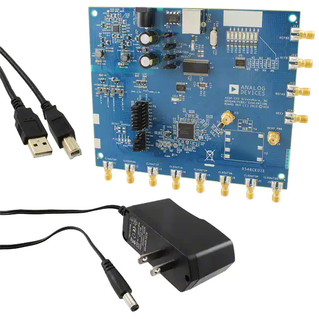
AD9548/PCBZ
1
Temperature Range
−40°C to +85°C
−40°C to +85°C
−40°C to +85°C
Package Description
88-Lead Lead Frame Chip Scale Package [LFCSP_VQ]
88-Lead Lead Frame Chip Scale Package [LFCSP_VQ]
Evaluation Board
Z = RoHS Compliant Part.
©2009–2014 Analog Devices, Inc. All rights reserved. Trademarks and
registered trademarks are the property of their respective owners.
D08022-0-12/14(G)
Rev. G | Page 111 of 111
Package Option
CP-88-2
CP-88-2
CP-88-2
�