Single-Channel, 16-Bit, Current/Voltage Output DAC,
Functional Safety Approved for Unipolar Current Output
ADFS5758
Data Sheet
FEATURES
Functional safety approved to SIL 2/SC3 for unipolar current
output by TÜV Rheinland, File Number 968/FSP
2055.00/20
Current/voltage output available on a single terminal
Current output ranges: 0 mA to 20 mA, 4 mA to 20 mA,
0 mA to 24 mA, ±20 mA, ±24 mA, −1 mA to +22 mA
Voltage output ranges (with 20% overrange): 0 V to 5 V,
0 V to 10 V, ±5 V, and ±10 V
Advanced on-chip diagnostics
12-bit ADC functioning as an independent monitoring
function that can validate the output and accuracy.
On-chip reference
DPC for thermal management
User-programmable offset and gain
Robust architecture, including output fault protection
EMC test standards
IEC 61000-4-6 conducted immunity (10 V, Class A)
IEC 61000-4-3 radiated immunity (20 V/m, Class A)
IEC 61000-4-2 ESD (±6 kV contact, Class B)
IEC 61000-4-4 electrical fast transient (EFT) (±4 kV, Class B)
IEC 61000-4-5 surge (±4 kV, Class B)
CISRP 11 radiated emissions (Class B)
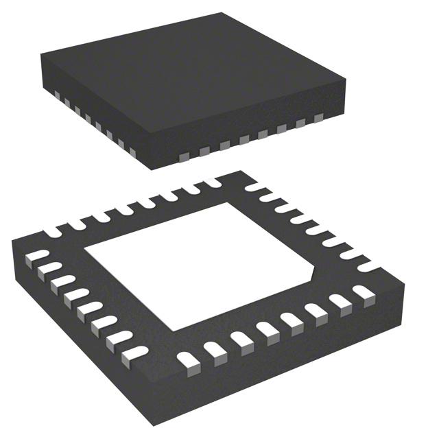
32-lead, 5 mm × 5 mm LFCSP
−40°C to +105°C temperature range
APPLICATIONS
configuration. The safe state for the ADFS5758 is open circuit/high
impedance.
The ADFS5758 is a single-channel, voltage and current output
digital-to-analog converter (DAC) that operates with a power
supply range from −33 V minimum on AVSS to +33 V maximum
on AVDD1 with a maximum operating voltage between the two rails
of 60 V. On-chip dynamic power control (DPC) minimizes
package power dissipation, which is achieved by regulating the
supply voltage (VDPC+) to the VIOUT output driver circuitry from
4.95 V to 27 V using a buck dc-to-dc converter, optimized for
minimum on-chip power dissipation. The CHART pin enables a
HART® signal to be coupled onto the current output.
The device uses a versatile 4-wire serial peripheral interface (SPI)
that operates at clock rates of up to 50 MHz and is compatible with
standard SPI, QSPI™, MICROWIRE™, DSP, and microcontroller
interface standards. The interface also features an optional SPI
cyclic redundancy check (CRC) and a windowed watchdog timer.
The ADFS5758 offers improved diagnostic features from its
predecessors, such as an integrated independent 12-bit diagnostic
analog-to-digital converter (ADC) that can be used to digitize both
internal and external nodes.
PRODUCT HIGHLIGHTS
1.
2.
Process control
Actuator control
Channel isolated analog outputs
Programmable logic controller (PLC) and distributed control
system (DCS) applications
HART network connectivity
3.
GENERAL DESCRIPTION
5.
The ADFS5758 is a single-channel, 16-bit, current/voltage output
DAC. The device is functional safety approved for unipolar current
output and is a fully compliant item with a systematic capability of
SC3, which can be used in safety-related applications up to SIL 2,
according to IEC 61508. This arrangement allows a single
ADFS5758 to be used to achieve SIL 2 for a nonredundant
Rev. 0
4.
Functional safety approved to SIL 2/SC3 by TÜV Rheinland.
Range of advanced diagnostic features, including an
integrated ADC for high reliability.
DPC using an integrated buck dc-to-dc converter for thermal
management. When used with the ADP1031, the ADFS5758
enables eight channel to channel isolated outputs at 90%. A detailed
description of the configuration, operation, SFF calculations,
FIT data, and other required metrics for the ADFS5758 in a
functionally safe application can be found in the ADFS5758
Safety Manual (available by request). Die and pin FME(D)As
have also been completed and are available (in addition to the
Safety Manual) on request from Analog Devices, Inc.
The voltage ranges available are 0 V to 5 V, ±5 V, 0 V to 10 V,
and ±10 V. A 20% overrange feature is also available (via the
DAC_CONFIG register) as well as the facility to negatively
offset the unipolar voltage ranges via the GP_CONFIG1
register (see the General-Purpose Configuration 1 Register
section).
DAC ARCHITECTURE
Reference
The DAC core architecture of the ADFS5758 consists of a
voltage mode R-2R ladder network. The voltage output of the
DAC core is converted to either a current or voltage output at
the VIOUT pin. Only one mode can be enabled at any one time.
Both the voltage and current output stages are supplied by the
VDPC+ power rail (internally generated from AVDD1) and the
AVSS rail.
The ADFS5758 can operate with either an external or internal
reference. The reference input requires a 2.5 V reference for
specified performance. This input voltage is then internally
buffered before it is applied to the DAC.
Current Output Mode
If current output mode is enabled, the voltage output from the
DAC is converted to a current (see Figure 74), which is then
mirrored to the supply rail so that the application only sees a
current source output.
21790-023
AVSS
IOUT
OPEN FAULT
Figure 74. Voltage-to-Current Conversion Circuitry
Voltage Output Mode
If voltage output mode is enabled, the voltage output from the
DAC is buffered and scaled to output a software-selectable
unipolar or bipolar voltage range (see Figure 75).
+VSENSE
DAC
RANGE
SCALING
VIOUT
–VSENSE
21790-024
VOUT SHORT FAULT
Figure 75. Voltage Output
The ADFS5758 contains an integrated buffered 2.5 V voltage
reference that is externally available for use elsewhere within
the system. The internal reference drives the integrated 12-bit
ADC. REFOUT must be connected to REFIN to use the
internal reference to drive the DAC.
Rev. 0 | Page 31 of 75
�ADFS5758
Data Sheet
Power-On Reset
SERIAL INTERFACE
AVDD2
The ADFS5758 is controlled over a versatile 4-wire serial
interface that operates at clock rates of up to 50 MHz and is
compatible with SPI, QSPI, MICROWIRE, and DSP standards.
Data coding is always straight binary.
VLDO
3.3V
VLDO
SYNC
SCLK
SDI
SOFTWARE
RESET
RESET
HARDWARE
RESET
INT_AVDD
Input Shift Register
Table 7. Writing to a Register (CRC Enabled)
MSB
D31
Slip Bit
D30:D29
ADFS5758
address
D28:D24
Register
address
D23:D8
Data
LSB
D7:D0
CRC
Transfer Function
Table 8 shows the input code to ideal output voltage relationship for the ADFS5758 for straight binary data coding of the
±5 V output range.
Table 8. Ideal Output Voltage to Input Code Relationship
Digital Input, Straight Binary
Data Coding
MSB
LSB
1111 1111
1111
1111
1111 1111
1111
1110
1000 0000
0000
0000
0000 0000
0000
0001
0000 0000
0000
0000
Analog Output
VOUT
+2 × VREF × (32,767/32,768)
+2 × VREF × (32,766/32,768)
0V
−2 × VREF × (32,767/32,768)
−2 × VREF
POWER-ON STATE OF THE ADFS5758
On initial power-on or a device reset, the voltage and current
output channel is disabled. The switch connecting VIOUT via a
30 kΩ pull-down resistor to AGND is open. This switch can be
configured in the DCDC_CONFIG2 register. VDPC+ is internally
driven to 4.8 V on power-on until the dc-to-dc converter is
enabled.
After device power-on, or a device reset, a calibration memory
refresh command is required (see the Echo Mode section). It is
recommended to wait 500 µs minimum after writing this
command, before writing further instructions to the device to
allow time for internal calibrations to take place (see Figure 93).
POWER-ON
RESET
21790-125
With SPI CRC enabled (default state), the input shift register is
32 bits wide. Data is loaded into the device MSB first as a 32-bit
word under the control of a serial clock input, SCLK. Data is
clocked in on the falling edge of SCLK. If CRC is disabled, the
serial interface is reduced to 24 bits. A 32-bit frame is still
accepted, but the last eight bits are ignored. See the Register
Map section for full details on the registers that can be
addressed via the SPI interface.
Figure 76. Power-On Reset Block Diagram
The ADFS5758 incorporates a power-on reset circuit that
ensures the ADFS5758 is held in reset while the power supplies
are at a level insufficient to allow reliable operation. The poweron reset circuit (see Figure 76) monitors the AVDD2 generated
VLDO and INT_AVCC voltages, the RESET pin, and the SPI
reset signal. The power-on reset circuit keeps the ADFS5758 in
reset until the voltages on the VLDO, and INT_AVCC nodes
are sufficient for reliable operation. If the power-on circuit
receives a signal from the RESET pin or if a software reset is
written to the ADFS5758 via the SPI interface, the ADFS5758 is
reset. Do not write SPI commands to the device within 100 μs
of a reset event.
POWER SUPPLY CONSIDERATIONS
The ADFS5758 has four supply rails: AVDD1, AVDD2, AVSS, and
VLOGIC. See the Specifications section for the voltage range of the
four supply rails and the associated conditions.
AVDD1 Considerations
AVDD1 is the supply rail for the dc-to-dc converter and can
range from 7 V to 33 V. Although the maximum value of AVDD1
is 33 V and the minimum value of AVSS is −33 V, the maximum
operating range of |AVDD1 to AVSS| is 60 V. VDPC+ is derived
from AVDD1, and its value depends on the mode of operation of
the dc-to-dc converter.
The dc-to-dc converter requires a sufficient level of margin to
be maintained between AVDD1 and VDPC+ to ensure the dc-to-dc
circuitry operates correctly. This margin is 5% of the maximum
VDPC+ voltage for a given mode of operation.
Table 9. AVDD1 to VDPC+ Margin
Mode of Operation VDPC+ Maximum
DPC Voltage Mode
15 V
DPC Current Mode
(IOUT maximum × RLOAD) + IOUT headroom
DCDC_CONFIG1, Bits[4:0] programmed
PPC Current Mode
value
See the Power Dissipation Control section for further details on
the dc-to-dc converter modes of operation.
Rev. 0 | Page 32 of 75
�Data Sheet
ADFS5758
Calculating Supply Voltage
AVSS Considerations
Assuming DPC current mode, use the following equations to
calculate the voltage and current values:
AVSS is the negative supply rail and has a range of −33 V to
0 V. As in the case of AVDD1, AVSS must obey the maximum
operating range of |AVDD1 to AVSS| of 60 V. For bipolar current
output ranges, the maximum AVSS can be calculated as (IOUT_MAX ×
RLOAD) + IOUT footroom. For unipolar current output ranges,
AVSS can be tied to AGND (that is, 0 V). For unipolar voltage
output ranges, the maximum AVSS is −2 V to enable sufficient
footroom for the internal voltage output circuitry. To avoid
power supply sequencing issues, a Schottky diode must be
placed between AVSS and GND (the GND supply must always
be available).
VDPC+ Maximum = IOUT Maximum Voltage +
IOUT Headroom = 22.5 V
where:
IOUT Maximum = 20 mA (RLOAD = 1 kΩ).
IOUT Maximum Voltage is IOUT Maximum × RLOAD = 20 V.
IOUT Headroom = 2.5 V.
|VDPC+ to AVDD1| headroom can be calculated as 5% of 22.5 V =
1.125 V. Therefore, AVDD1 minimum = 22.5 V + 1.125 V =
23.625 V. Assuming a worst case AVDD1 supply rail tolerance
of ±10%, this example requires an AVDD1 supply rail of
approximately 26.25 V.
AVDD2 Considerations
AVDD2 is the positive low voltage supply rail and has a range of
5 V to 33 V. If only one positive power rail is available, AVDD2
can be tied to AVDD1. However, to optimize for reduced power
dissipation, supply AVDD2 with a separate lower voltage supply.
VLOGIC Considerations
VLOGIC is the digital supply for the device and can range from
1.71 V to 5.5 V. The 3.3 V VLDO output voltage can be used to
drive VLOGIC.
Rev. 0 | Page 33 of 75
�ADFS5758
Data Sheet
DEVICE FEATURES AND DIAGNOSTICS
POWER DISSIPATION CONTROL
The ADFS5758 contains integrated buck dc-to-dc converter
circuitry that controls the power supply to the output buffers,
allowing reductions in power consumption from standard
designs when using the device in both current and voltage
output modes. AVDD1 is the supply rail for the dc-to-dc converter
and can range from 7 V to 33 V. VDPC+ is derived from this rail
and its value depends on the mode of operation of the dc-to-dc
converter as well as the output load, including DPC voltage
mode, DPC current mode, and PPC current mode.
Figure 77 shows the discrete components needed for the dc-todc circuitry and the following sections describe component
selection and operation of this circuitry.
0.1µF
CIN
4.7µF
AVDD1
CDCDC
2.2µF
PGND1
LDCDC
47µH
SW+
VDPC+
PGND1
21790-021
DC-TO-DC
CONVERTER
CIRCUITRY
VDPC+
Figure 77. DC-to-DC Circuit
Table 10. Recommended DC-to-DC Components
Symbol
Component
Value
Manufacturer
LDCDC
CDCDC
CIN
LPS4018-473MRB
GCM31CR71H225KA55L
GRM31CR71H475KA12L
47 μH
2.2 μF
4.7 μF
Coilcraft
Murata
Murata
DC-to-DC Converter Operation
The dc-to-dc converter uses a fixed 500 kHz frequency, peak
current mode control scheme to step down the AVDD1 input to
produce VDPC+ to supply the driver circuitry of the voltage/current
output channel. The dc-to-dc converter incorporates a low-side
synchronous switch and, therefore, does not require an external
Schottky diode. The dc-to-dc converter is designed to operate
predominantly in discontinuous conduction mode (DCM),
where the inductor current goes to zero for an appreciable
percentage of the switching cycle. To avoid generating lower
frequency harmonics on the VDPC+ regulated output voltage rail,
the dc-to-dc converter does not skip any cycles. Therefore, the
dc-to-dc converter must transfer a minimum amount of energy
to its load (that is, the current or voltage output stage and its
respective load) to operate at a fixed frequency. Thus, for light
loads (for example, low RLOAD or low IOUT), the VDPC+ voltage can
rise beyond the target value and go out of regulation. This is
not a fault condition and does not represent the worst case
power dissipation condition in an application.
Note that the dc-to-dc converter requires a sufficient level of
margin to be maintained between AVDD1 and VDPC+ to ensure
the dc-to-dc circuitry operates correctly. This margin value is
5% of VDPC+ maximum.
DPC Voltage Mode
In DPC voltage mode, with the voltage output enabled or
disabled, the converter regulates the VDPC+ supply to 15 V above
the −VSENSE voltage. This mode allows the full output voltage
range to be efficiently applied across remote loads, with
corresponding remote grounds at up to ±10 V potential relative
to the local ground supply (AGND) for the ADFS5758.
DPC Current Mode
In standard current input module designs, the combined line
and load resistance values can range from typically 50 Ω to
750 Ω. Output module systems must provide enough voltage to
meet the compliance voltage requirement across the full range
of load resistor values. For example, in a 4 mA to 20 mA loop,
when driving 20 mA into a 750 Ω load, a compliance voltage of
>15 V is required. When driving 20 mA into a 50 Ω load, the
required compliance is reduced to >1 V.
In DPC current mode, the ADFS5758 dc-to-dc circuitry senses
the output voltage and regulates the VDPC+ supply voltage to meet
compliance requirements plus an optimized headroom voltage
for the output buffer. VDPC+ is dynamically regulated to 4.95 V
or (IOUT × RLOAD + headroom), whichever is greater. This regulation
excludes the light load condition whereby the VDPC+ voltage can
rise beyond the target value, which does not represent the worst
case power dissipation condition in an application. The
ADFS5758 is capable of driving up to 24 mA through a 1 kΩ
load, for a given input supply (24 V + headroom).
At low output power levels, the regulated headroom increases
above 2.3 V because the dc-to-dc circuitry uses a minimum on
time ADFS5758 cycle. This behaviour is expected and does not
impact any worse case power dissipation.
PPC Current Mode
The dc-to-dc converter can also operate in programmable power
control mode, where the VDPC+ voltage is user programmable to a
given level to accommodate the maximum output load required.
This mode represents a trade-off between the optimized power
efficiency of the DPC current mode and the settling time of a
system with a fixed supply (dc-to-dc disabled). In PPC current
mode, VDPC+ is regulated to a user-programmable level between 5 V
and 25.677 V with respect to −VSENSE (in steps of 0.667 V). This
mode is useful if settling time is an important requirement of the
design. See the DC-to-DC Converter Settling Time section. Care
is needed in selecting the programmed level of VDPC+ if the load
is nonlinear in nature. VDPC+ must be set high enough to obey the
output compliance voltage specification. If the load is unknown,
the +VSENSE input to the ADC can be used to monitor the VIOUT pin
in current mode to determine the user-programmable value at
which to set VDPC+.
Rev. 0 | Page 34 of 75
�Data Sheet
ADFS5758
DC-to-DC Converter Settling Time
When in DPC current mode, the settling time is dominated by the
settling time of the dc-to-dc converter and is typically 200 µs
without the digital slew rate control feature enabled. To reduce
initial VIOUT waveform overshoot without adding a capacitor on
VIOUT and thereby affecting HART operation, enable the digital
slew rate control feature using the DAC_CONFIG register (see
Table 34).
Table 11 shows the typical settling time for each of the dc-to-dc
converter modes. All values shown assume the use of the
components recommended by Analog Devices listed in Table 10.
The achievable settling time in any given application is dependent
on the choice of external inductor and capacitor components
used, as well as the current-limit setting of the dc-to-dc
converter.
Table 11. DC-to-DC Converter Mode vs. Settling Time
DC-to-DC Converter Mode
DPC Current Mode
PPC Current Mode
DPC Voltage Mode
Settling Time (µs)
200
15
15
DC-to-DC Converter Inductor Selection
For typical 4 mA to 20 mA applications, a 47 μH inductor (per
Table 10), combined with the switching frequency of 500 kHz,
allows up to 24 mA to be driven into a load resistance of up to 1 kΩ
with an AVDD1 supply of greater than 24 V + headroom. It is
important to ensure that the peak current does not cause the
inductor to saturate, especially at the maximum ambient
temperature. If the inductor enters saturation mode, it results in a
decrease in efficiency. Larger size inductors translate to lower core
losses. The slew rate control feature of the ADFS5758 can be used
to limit peak currents during slewing. Program an appropriate
current limit (via the DCDC_CONFIG2 register) to shut off the
internal switch if the inductor current reaches that limit.
DC-to-DC Converter Input and Output Capacitor
Selection
The output capacitor, CDCDC, affects the ripple voltage of the dcto-dc converter and limits the maximum slew rate at which the
output current can rise. The ripple voltage is directly related to
the output capacitance. The CDCDC capacitor recommended by
Analog Devices (see Table 10), combined with the recommended
47 µH inductor, results in a 500 kHz ripple with amplitude less
than 50 mV and guarantees stability and operation with HART
capability across all operating modes.
For high voltage capacitors, the size of the capacitor is often a
good indication of its charge storage ability. It is important to
characterize the dc bias voltage vs. capacitance curve for this
capacitor. Any capacitance values specified are with reference
to a dc bias corresponding to the maximum VDPC+ voltage in the
application. As well as the voltage rating, the temperature range
of the capacitor must also be considered for a given application.
These considerations are key in selection of the components
described in Table 10.
The input capacitor, CIN, provides much of the dynamic current
required for the dc-to-dc converter, and a low effective series
resistance (ESR) component is recommended. For the ADFS5758,
a low ESR tantalum or ceramic capacitor of 4.7 μF (1206 size) in
parallel with a 0.1 μF (0402 size) capacitor is recommended.
Ceramic capacitors must be chosen carefully because they can
exhibit a large sensitivity to dc bias voltages and temperature.
X5R or X7R dielectrics are preferred because these capacitors
remain stable over wider operating voltage and temperature
ranges. Care must be taken if selecting a tantalum capacitor to
ensure a low ESR value.
CLKOUT
The ADFS5758 provides a CLKOUT signal to the system for
synchronization purposes. This signal is programmable to eight
frequency options between 416 kHz and 588 kHz, with the default
option being 500 kHz—the same switching frequency of the dcto-dc converter. This feature is configured in the GP_CONFIG1
register and is disabled by default.
INTERDIE 3-WIRE INTERFACE
A 3-wire interface is used to communicate between the two die
in the ADFS5758. The 3-wire interface master is located on the
main die, and the 3-wire interface slave is on the dc-to-dc die.
The three interface signals are data, DCLK (running at
MCLK/8), and interrupt.
The main purpose of the 3-wire interface is to read from or write
to the DCDC_CONFIG1 and DCDC_CONFIG2 registers.
Addressing these registers via the SPI interface initiates an
internal 3-wire interface transfer from the main die to the dcto-dc die. The 3-wire interface master on the main die initiates
writes and reads to the registers on the dc-to-dc die using DCLK as
the serial clock. The slave uses an interrupt signal to indicate a
read of the internal status register of the dc-to-dc die is required.
For every 3-wire interface write, an automatic read and compare
process can be enabled (default case) to ensure that the contents of
the copy of the DCDC_CONFIGx registers on the main die
match the contents of the registers on the dc-to-dc die. This
comparison is performed to ensure the integrity of the digital
circuitry on the dc-to-dc die. With this feature enabled, a 3-wire
interface transfer takes approximately 300 µs. When disabled,
this transfer time reduces to 30 µs.
The BUSY_3WI flag in the DCDC_CONFIG2 register is asserted
during the 3-wire interface transaction. The BUSY_3WI flag
is also set when the user updates the DAC range (via the DAC_
CONFIG register, Bits[4:0]) due to the internal calibration
memory refresh caused by this action, which requires a 3-wire
interface transfer between the two die. A write to either of the
DCDC_CONFIGx registers must not be initiated while
BUSY_3WI is asserted. If a write occurs, the new write is
delayed until the current 3-wire interface (3WI) transfer
completes.
Rev. 0 | Page 35 of 75
�ADFS5758
Data Sheet
3-Wire Interface Diagnostics
+VSENSE
ADFS5758
Any faults on the dc-to-dc die triggers an interrupt to the main
die. An automatic status read of the dc-to-dc die is performed.
After the read transaction, the main die has a copy of the dc-todc die status bits (VIOUT_OV_ERR, DCDC_P_SC_ERR and
DCDC_P_PWR_ERR). These values are available in the
ANALOG_DIAG_RESULTS register and via the OR’ed analog
diagnostic results bits in the status register. These bits also
trigger the FAULT pin.
In response to the interrupt request, the main die (master)
performs a 3-wire interface read operation to read the status of
the dc-to-dc die. The interrupt is only asserted again by a
subsequent dc-to-dc die fault flag, upon which the 3-wire
interface initiates another status read transaction. If an interrupt
signal is detected six times in a row, the interrupt detection
mechanism is disabled until a 3-wire interface write transaction
completes. This disabling prevents the 3-wire interface from
being blocked because of the constant dc-to-dc die status read
when the interrupt is toggling. The INTR_SAT_3WI flag in the
DCDC_CONFIG2 register indicates when this event occurs, and a
write to either DCDC_CONFIGx register resets this bit to 0.
During a 3-wire read or write operation, the address and data bits
in the transaction produce parity bits. These parity bits are checked
on the receive side and if they do not match on both die, the
ERR_3WI bit in the DIGITAL_DIAG_RESULTS register is set.
If the read and compare process is enabled and a parity error
occurs, the BKGND_CRC_ERR bit in the DIGITAL_DIAG_
RESULTS register is also set.
16-BIT
DAC
2MΩ
VOUT
RANGE
SCALING
VIOUT
–VSENSE
±10V VCM
21790-121
2MΩ
RLOAD
REFIN
Figure 78. Voltage Output
Driving Large Capacitive Loads
The voltage output amplifier is capable of driving capacitive
loads of up to 2 µF with the addition of a 220 pF nonpolarized
compensation capacitor. This capacitor, while allowing the
ADFS5758 to drive higher capacitive loads and reduce overshoot,
increases the settling time of the device and, therefore, affects the
bandwidth of the system. Without the compensation capacitor,
capacitive loads up to 10 nF can be driven.
Voltage Output Short-Circuit Protection
Under normal operation, the voltage output sinks/sources up to
12 mA and maintains specified operation. The short-circuit
current is typically 15 mA. If a short circuit is detected, the
FAULT pin goes low and the VOUT_SC_ERR bit in the
ANALOG_DIAG_RESULTS register is set.
FAULT PROTECTION
VOLTAGE OUTPUT
The ADFS5758 incorporates a line protector on the VIOUT pin,
+VSENSE pin, and −VSENSE pin. The line protector operates by
clamping the voltage internal to the line protector to the VDPC+
and AVSS rails, thereby protecting internal circuitry from
external voltage faults. If a voltage outside of these limits is
detected on the VIOUT pin, an error flag (VIOUT_OV_ERR) is
also set and is located in the ANALOG_DIAG_RESULTS register.
Voltage Output Amplifier and VSENSE Functionality
CURRENT OUTPUT
The voltage output amplifier is capable of generating both unipolar
and bipolar output voltages, and is also capable of driving a load
of 1 kΩ in parallel with 2 µF (with an external compensation
capacitor) to AGND. Figure 78 shows the voltage output
driving a load, RLOAD, on top of a common-mode voltage (VCM)
of ±10 V. An integrated 2 MΩ resistor ensures the amplifier
loop is kept closed, thus preventing potential large destructive
voltages on VIOUT due to the broken amplifier loop in applications
where a cable can possibly become disconnected from +VSENSE. If
remote sensing of the load is not required, connect +VSENSE
directly to VIOUT and connect −VSENSE directly to AGND. Make
both connections using 1 kΩ resistors.
External Current Setting Resistor
The FAULT_INJECT_3WI bits (in the GP_CONFIG2 register)
can be used to check that the 3-wire interface diagnostics are
functioning correctly.
As shown in Figure 74, RSET is an internal sense resistor that forms
part of the voltage to current conversion circuitry. The stability
of the output current value over temperature is dependent on
the stability of the value of RSET. As a method of improving the
stability of the output current over temperature, an external
13.7 kΩ low drift resistor can be connected between the RA and
RB pins of the ADFS5758, to be used instead of the internal
resistor.
Table 1 shows the performance specifications of the ADFS5758
with both the internal RSET resistor and an external, 13.7 kΩ
RSET resistor. The external RSET resistor specification assumes an
ideal resistor. The actual performance depends on the absolute
value and temperature coefficient of the resistor used. The
resistor specifications, therefore, directly affect the gain error of
the output and the TUE.
Rev. 0 | Page 36 of 75
�Data Sheet
ADFS5758
To arrive at the absolute worst case overall TUE of the output
with a particular external RSET resistor, add the percentage
absolute error of the RSET resistor directly to the TUE of the
ADFS5758 with the external RSET resistor, shown in Table 1
(expressed in % FSR). The temperature coefficient also must
be considered, as well as the specifications of the external
reference, if this is the option being used in the system.
The magnitude of the error derived from simply summing the
absolute error and TC error of both the external RSET resistor and
the external reference with the TUE specification of the
ADFS5758 is unlikely to occur because the temperature
coefficients of the individual components are not likely to
exhibit the same drift polarity, and, therefore, an element of
cancelation occurs. For this reason, add the temperature
coefficients in a root of squares fashion. A further improvement
can be gained by performing a two-point calibration at zero
scale and full scale, thus reducing the absolute errors of the
voltage reference and the RSET resistor.
Current Output Open-Circuit Detection
When in current output mode, if the headroom available falls
below the compliance range due to an open-loop circuit or an
insufficient power supply voltage, the IOUT_OC_ERR flag in
the ANALOG_DIAG_RESULTS register is asserted, and the
FAULT pin goes low.
If the HART feature is not required, disable the HART_EN bit
and leave the CHART pin open circuit. However, if it is required
to slow the DAC output signal with a capacitor, the HART_EN
bit must be enabled and the required CSLEW capacitor connected
to the CHART pin.
DIGITAL SLEW RATE CONTROL
The slew rate control feature of the ADFS5758 allows the user
to control the rate at which the output value changes. This
feature is available in both current and voltage mode. With the
slew rate control feature disabled, the output value changes at a
rate limited by the output drive circuitry and the attached load.
To reduce the slew rate, enable the slew rate control feature.
With this feature enabled, the output steps digitally from one
value to the next at a rate defined by two parameters accessible
via the DAC_CONFIG register. The parameters are
SR_CLOCK and SR_STEP. SR_CLOCK defines the rate at
which the digital slew is updated. For example, if the selected
update rate is 8 kHz, the output updates every 125 µs. In
conjunction with SR_CLOCK, SR_STEP defines by how much
the output value changes at each update. Together, both
parameters define the rate of change of the output value.
The following equation describes the slew rate as a function of
the step size, the update clock frequency, and the LSB size:
Slew Time =
HART CONNECTIVITY
The ADFS5758 has a CHART pin, onto which a HART signal can
be coupled. The HART signal appears on the current output if
the HART_EN bit in the GP_CONFIG1 register is enabled and
the VIOUT output is also enabled.
Figure 79 shows the recommended circuit for attenuating
and coupling the HART signal to the ADFS5758. To achieve
1 mA p-p at the VIOUT pin, a signal of approximately 125 mV p-p is
required at the CHART pin. Note that the HART signal appearing
at the VIOUT pin is inverted relative to the signal input at the
CHART pin.
–
IOUT
RANGE
SCALING
IOUT
CHART
HART_EN
C1
C2
HART MODEM
OUTPUT
21790-027
16-BIT
DAC
Figure 79. Coupling the HART Signal
As well as their use in attenuating the incoming HART modem
signal, a minimum capacitance of the combination of C1 and
C2 is required to ensure that the bandwidth presented to the
modem output signal passes the 1.2 kHz and 2.2 kHz frequencies.
Assuming a HART signal of 500 mV p-p, the recommended
values are C1 = 47 nF and C2 = 150 nF. Digitally controlling the
slew rate of the output is necessary to meet the analog rate of
change requirements for HART.
Output Change
Step Size × Slew Rate Frequency × LSB Size
where:
Slew Time is expressed in seconds.
Output Change is expressed in amps for current output mode
or volts for voltage output mode.
Step Size is the LSB step size (for example, LSB = 20 mA
range/216).
Slew Rate Frequency is SR_CLOCK.
LSB Size is SR_STEP.
When the slew rate control feature is enabled, all output changes
occur at the programmed slew rate. For example, if the WDT
times out and an automatic clear occurs, the output slews to the
clear value at the programmed slew rate (setting the
CLEAR_NOW_EN bit in the GP_CONFIG1 register overrides
this default behavior to cause the output to update to the clear
code immediately rather than at the programmed slew rate).
The slew rate frequency for any given value is the same for all
output ranges. The step size, however, varies across output
ranges for a given value of step size because the LSB size is
different for each output range.
ADFS5758 ADDRESS PINS
The ADFS5758 address pins (AD0 and AD1) are used in
conjunction with the ADFS5758 address bits within the SPI
frame (see Table 12) to determine which ADFS5758 device is
being addressed by the system controller. Using the two
address pins, up to four devices can be independently
addressed on one board.
Rev. 0 | Page 37 of 75
�ADFS5758
Data Sheet
SPI INTERFACE AND DIAGNOSTICS
UPDATE ON SYNC HIGH
SYNC
The ADFS5758 is controlled over a 4-wire serial interface with
an 8-bit cyclic redundancy check (CRC-8) enabled by default.
The input shift register is 32 bits wide and data is loaded into
the device MSB first under the control of a serial clock input,
SCLK. Data is clocked in on the falling edge of SCLK. If CRC is
disabled, the serial interface is reduced to 24 bits. A 32-bit
frame is still accepted but the last eight bits are ignored.
Table 12. Writing to a Register (CRC Enabled)
D30:D29
ADFS5758
address
D28:D24
Register address
D23:D8
Data
MSB
D23
LSB
D0
SDI
24-BIT DATA
24-BIT DATA TRANSFER—NO CRC ERROR CHECKING
UPDATE ON SYNC HIGH
ONLY IF CRC CHECK PASSED
SYNC
LSB
D7:D0
CRC
SCLK
As shown in Table 12, every SPI frame contains two ADFS5758
address bits. These bits must match the hardware ADFS5758
address pins (AD0 and AD1) for a particular device to accept
the SPI frame on the bus.
MSB
D31
LSB
D8
SDI
D0
8-BIT CRC
FAULT PIN GOES LOW
IF CRC CHECK FAILS
FAULT
SPI Cyclic Redundancy Check
D7
24-BIT DATA
32-BIT DATA TRANSFER WITH CRC ERROR CHECKING
To verify that data has been received correctly in noisy environments, the ADFS5758 offers the option of a CRC based on an
8-bit cyclic redundancy check (CRC-8). The device controlling
the ADFS5758 generates an 8-bit frame check sequence using
the following polynomial:
C(x) = x8 + x2 + x1 + 1
This sequence is added to the end of the data-word, and 32 bits
are sent to the ADFS5758 before taking SYNC high.
If the SPI_CRC_EN bit is set high (default state), the user must
supply a frame of exactly 32 bits wide that contains the 24 data bits
and 8-bit CRC. If the CRC check is valid, the data is written to
the selected register. If the CRC check fails, the FAULT pin goes
low and the FAULT pin status and the digital diagnostic status bit
(DIG_DIAG_STATUS) in the status register are set. A subsequent
readback of the DIGITAL_DIAG_RESULTS register reveals that
the SPI_CRC_ERR bit is also set. This register is a per bit, write
to clear register (see the Sticky Diagnostic Results Bits section).
Therefore, the SPI_CRC_ERR bit can be cleared by writing a 1
to Bit D0 of the DIGITAL_DIAG_RESULTS register. Doing so
clears the SPI_CRC_ERROR bit and causes the FAULT pin to
return high (assuming that there are no other active faults).
When configuring the FAULT_PIN_CONFIG register, the user
can decide whether the SPI CRC error affects the FAULT pin.
See the FAULT Pin Configuration Register section for further
details. The SPI CRC feature can be used for both the
transmission and receipt of data packets.
21790-025
MSB
D31
Slip bit
SCLK
Figure 80. CRC Timing (Assume LDAC = 0)
SPI Interface Slip Bit
A further enhancement to the robustness of the interface is the
addition of the slip bit. The MSB of the SPI frame must equal
the inverse of MSB − 1 for the frame to be considered valid. If
an incorrect slip bit is detected, the data is ignored and the
SLIPBIT_ERR bit in the DIGITAL_DIAG_RESULTS register is
asserted.
SPI Interface SCLK Count Feature
An SCLK count feature is also built into the SPI diagnostics,
meaning that only SPI frames with exactly 32 SCLK falling
edges (24 or 32 if SPI CRC is enabled) are accepted by the
interface as a valid write. SPI frames of lengths other than
these are ignored and the SCLK_COUNT_ERR flag asserts
in the DIGITAL_DIAG_RESULTS register.
Readback Modes
The ADFS5758 offers four readback modes, as follows:
•
•
•
•
Two-stage readback mode
Autostatus readback mode
Shared SYNC autostatus readback mode
Echo mode
The two stage readback consists of a write to a dedicated
register, TWO_STAGE_READBACK_SELECT, to select the
register location to be read back. This write is followed by a
no operation (NOP) command, during which the contents of
the selected register are available on SDO.
Table 13. SDO Contents for Read Operation
MSB
LSB
[D31:D30] D29
[D28:24]
[D23:D8] [D7:D0]
Register
Data
CRC
0b10
FAULT pin
address
status
Rev. 0 | Page 38 of 75
�Data Sheet
ADFS5758
Bits[D31:D30] = 0b10 are used for synchronization purposes
during readback.
If autostatus readback mode is selected, the contents of the status
register is available on the SDO line during every SPI transaction.
This ability allows the user to continuously monitor the status
register and act quickly in the case of a fault. The ADFS5758
powers up with this feature disabled. When this feature is enabled,
the normal two-stage readback feature is not available. Only the
status register is available on SDO. To read back any other
register, disable the automatic readback feature first before
following the two-stage readback sequence. The automatic
status readback can be reenabled after the register is read back.
The shared SYNC autostatus readback is a special version of the
autostatus readback mode used to avoid SDO bus contention
when multiple devices are sharing the same SYNC line.
PREVIOUS
COMMAND
STATUS
REGISTER
CONTENTS
PREVIOUS
COMMAND
21790-019
Echo mode behaves similarly to autostatus readback mode,
except that every second readback consists of an echo of the
previous command written to the ADFS5758 (see Figure 81).
See the Reading from Registers section for further details on the
readback modes.
Figure 81. SDO Contents, Echo Mode
registered as a fault. The windowing feature of the WDT can be
disabled by setting the window width to 1/1. In this scenario,
the user must simply kick the WDT any time before the center
threshold, eliminating the possibility of an early reset and thus
simplifying the operation of the WDT. For highest safety, the
window feature requires that the user write the correct key (or
two keys, if enabled) within the timeout window. If the signal
arrives before or after this timing window, the watchdog times
out and a dedicated WDT_STATUS bit in the status register alerts
the user that the WDT has timed out. The DIGITAL_DIAG_
RESULTS register can be read to clarify whether the WDT
timeout was due to a late or early kick. Note that, when a WDT
timeout occurs, all writes to the DAC_INPUT register as well as
hardware or software LDAC events are ignored until the active
WDT fault flag within the DIGITAL_DIAG_RESULTS register
is cleared. Once this flag has been cleared the WDT can be
restarted by performing a subsequent WDT kick command.
On power-up, the WDT is disabled by default. The default settings
of the center threshold and window width are 1 sec and 1/1,
respectively. The default method to kick the WDT is to write
one specific key and, upon timeout, the default action is to set
the relevant flag bits and the FAULT pin. See Table 41 for
specific register bit details to support the configurability of the
WDT operation.
WINDOWED WATCHDOG TIMER (WDT)
USER DIGITAL OFFSET AND GAIN CONTROL
This watchdog timer feature is useful to ensure that communication has not been lost between the system controller and the
ADFS5758 and that the SPI datapath lines are functioning as
expected.
The ADFS5758 has a USER_GAIN and a USER_OFFSET register
that allow trimming of the gain and offset errors from the
entire signal chain. The 16-bit USER_GAIN register allows the
user to adjust the gain of the DAC channel in steps of 1 LSB. The
USER_GAIN register coding is straight binary, as shown in
Table 14. The default code in the USER_GAIN register is 0xFFFF,
which results in no gain factor applied to the programmed
output. In theory, the gain can be tuned across the full range of
the output. In practice, the maximum recommended gain trim
is approximately 50% of the programmed range to maintain
accuracy.
•
•
•
A valid SPI write to any register.
A specific key code write to the key register (default).
Two specific consecutive key code writes to the key register.
As shown in Figure 82, the watchdog timer uses a center
threshold and a window width, where the width is a fraction of
the center threshold. For example, if the center threshold is set
to 100 ms and the window width set to 1/2, the valid region is
100 ms ± 25 ms. A WDT kick before 75 ms or after 125 ms is
CENTER THRESHOLD –
WINDOW WIDTH/2
FAULT: A RESET HERE
IS TOO EARLY
Table 14. Gain Register Adjustment
Gain Adjustment Factor
1
65,535/65,536
…
2/65,536
1/65,536
D15
1
1
…
0
0
CENTER THRESHOLD +
WINDOW WIDTH/2
MUST RESET HERE
FAULT: RESET IS
TOO LATE
CENTER THRESHOLD
Figure 82. Windowed Watchdog Timer
Rev. 0 | Page 39 of 75
21790-029
When enabled, the WDT alerts the system if the ADFS5758 does
not receive a specific SPI frame in the user-programmable timeout
period. A valid watchdog kick is a specific SPI frame received
within the pass window of the WDT. When the specific SPI
frame is received, the watchdog resets the timer controlling the
timeout alert. The SPI frame used to reset the WDT is
configurable as one of three choices:
D14 to D1
1
1
…
0
0
D0
1
0
…
1
0
�ADFS5758
Data Sheet
The 16-bit USER_OFFSET register allows the user to adjust the
offset of the DAC channel by −32,768 LSBs to +32,768 LSBs in
steps of 1 LSB. The USER_OFFSET register coding is straight
binary as shown in Table 15. The default code in the USER_
OFFSET register is 0x8000, which results in zero offset
programmed to the output.
DAC OUTPUT UPDATE AND DATA INTEGRITY
DIAGNOSTICS
Table 15. Offset Register Adjustment
The DAC_OUTPUT register (and ultimately the DAC output)
updates in any of the following cases:
Gain Adjustment
+32,768 LSBs
+32,767 LSBs
…
No Adjustment (Default)
…
−32,767 LSBs
−32,768 LSBs
D15
1
1
…
1
…
0
0
D13 to D2
1
1
…
0
…
0
0
D0
1
0
…
0
…
1
0
The value (in decimal) that is written to the internal DAC
register can be calculated by
DAC _ Code = D ×
( M + 1)
216
+ C − 215
Figure 83 shows a simplified version of the DAC input loading
circuitry. If used, the USER_GAIN and USER_OFFSET
registers must be updated before writing to the DAC_INPUT
register.
•
If a write is performed to the DAC_INPUT register with
the hardware LDAC pin tied low, the DAC_OUTPUT
register is updated on the rising edge of SYNC (subject to
the timing specifications in Table 2.
•
If the hardware LDAC pin is high and a write to the
DAC_INPUT register occurs, the DAC_OUTPUT register
does not update until a software LDAC instruction is
issued or the hardware LDAC pin is pulsed low.
If a WDT timeout occurs with the CLEAR_ON_WDT_FAIL
bit set, the CLEAR_CODE register contents are loaded to
the DAC_OUTPUT register.
If the slew rate control feature is enabled, the
DAC_OUTPUT register contains the dynamic value of the
DAC as it slews between values.
•
(1)
where:
D is the code loaded to the DAC_INPUT register.
M is the code in the USER_GAIN register (default code = 216 − 1).
C is the code in the USER_OFFSET register (default code = 215).
Data from the DAC_INPUT register is processed by a digital
multiplier and adder, controlled by the contents of the user
gain and USER_OFFSET registers, respectively. The calibrated
DAC data is then loaded to the DAC, dependent on the state of
the LDAC pin.
Each time data is written to the USER_GAIN or USER_
OFFSET register, the DAC output is not automatically updated.
Instead, the next write to the DAC_INPUT register uses these
user gain and user offset values to perform a new calibration
and automatically updates the channel. The read only
DAC_OUTPUT register represents the value currently
available at the DAC output except in the case of user gain and
user offset calibration. In this case, the DAC_OUTPUT register
represents the DAC data input by the user, on which the
calibration was performed and not the result of the calibration.
Both the USER_GAIN register and the USER_OFFSET register
have 16 bits of resolution. The correct method to calibrate the
gain and offset is to first calibrate the gain and then calibrate
the offset.
•
Note that, while a WDT fault is active, all writes to the DAC_
INPUT register as well as hardware or software LDAC events
are ignored. If the CLEAR_ON_WDT_FAIL bit was set, such
that the output was set to the clear code, when the WDT fault
flag is cleared, the DAC_INPUT register must be written to
before an update to the DAC_OUTPUT register occurs, that is,
performing a software or hardware LDAC only reloads the DAC
with the clear code. As described in the Echo Mode section, after
configuring the DAC range (via the DAC_CONFIG register), a
write to the DAC_INPUT register must occur, even if the contents
of the DAC_INPUT register are not changing from their current
value.
Note also that the GP_CONFIG2 register contains a bit to enable a
global software LDAC mode, whereby the ADFS5758 address
bits of the SW_LDAC command are ignored, thus enabling
multiple ADFS5758 devices to be simultaneously updated using
a single SW_LDAC command. This is a useful feature if the
hardware LDAC pin is not being used in a system containing
multiple ADFS5758 devices.
Rev. 0 | Page 40 of 75
�Data Sheet
ADFS5758
REFIN
OUTPUT
AMPLIFIER
DAC OUTPUT
REGISTER
(READ ONLY)
16-BIT
DAC
VIOUT
LDAC
(HARDWARE OR SOFTWARE)
CLEAR EVENT
(WDT TIMEOUT)
USER
GAIN AND OFFSET
CALIBRATION
SCLK
SYNC
SDI
DAC INPUT
REGISTER
INTERFACE LOGIC
SDO
21790-026
CLEAR CODE
REGISTER
Figure 83. Simplified Serial Interface of Input Loading Circuitry
DAC Data Integrity Diagnostics
LOCKABLE USER CONFIGURATION SPACE
To protect against transient changes to the internal digital
circuitry, the digital block stores both the digital DAC value
and an inverted copy of the digital DAC value. A check is
completed to ensure that the two values correspond to each
other before the DAC is strobed to update to the DAC code.
This feature is enabled by default (INVERSE_DAC_CHECK_
EN bit in the DIGITAL_DIAG_CONFIG register).
The ADFS5758 user configuration resisters listed in Table 16
have the feature of being lockable as read only. This means that
if locked, any writes to these registers are ignored and flagged in
the DIGITAL_DIAG_RESULTS register via the CFG_LOCK_
CHECK_ERR bit (if enabled) and via the FAULT pin.
Another optional diagnostic feature is the internal dual calibration
feature. This feature is enabled by setting the DUAL_CAL_EN
bit in the DIGITAL_DIAG_CONFIG register. When enabled,
the internal calibration on the 16-bit user DAC code is completed
twice. The DAC is only updated when both results match. If a
fail is registered, no DAC write occurs and the DUAL_CAL_
ERR flag is set.
Outside of the digital block, the DAC code is stored in latches
(as shown in Figure 84). These latches are potentially
vulnerable to the same transient events as those protected
against within the digital block. To protect the DAC latches
against such transients, the DAC latch monitor feature can be
enabled via the DAC_LATCH_MON_EN bit within the
DIGITAL_DIAG_CONFIG register. This feature monitors the
actual digital code driving the DAC and compares it with the
digital code generated within the digital block. Any difference
between the two codes causes the DAC_LATCH_MON_ERR flag
to be set in the DIGITAL_DIAG_RESULTS register.
DAC LATCHES
D
Q
D
Q
16-BIT
DAC
Q
Q
Figure 84. DAC Data Integrity
21790-028
DIGITAL
BLOCK
Note that the VLDO external capacitor detection feature must
not be enabled prior to locking the configuration register space
because this is a self clearing bit and causes the CFG_LOCK_
CHECK_ERR bit to flag if the corresponding value changes
subsequent to locking the configuration register space.
The user must write Data 0x4765 to the key register to lock the
registers. To unlock the registers, two unlock keys must be
written to the key register. The first key is Data 0x896D, and the
second key is Data 0x57AB. The unlock keys must be written to
the key register in that order.
The CFG_LOCK_CHECK_EN bit in the DIGITAL_DIAG_
CONFIG register must be set to enable flagging of an attempt
to write to a locked register via the CFG_LOCK_CHECK_ERR bit
in the DIGITAL_DIAG_RESULTS register. If the CFG_LOCK_
CHECK_EN bit is not set, the user has no indication that a
write was attempted to the locked registers.
Table 16. Lockable Registers
Address
Register
0x03
CLEAR_CODE
0x04
USER_GAIN
0x05
USER_OFFSET
0x06
DAC_CONFIG
0x09
GP_CONFIG1
0x0A
GP_CONFIG2
0x0B
DCDC_CONFIG1
0x0C
DCDC_CONFIG2
0x0F
WDT_CONFIG
0x10
DIGITAL_DIAG_CONFIG
0x11
ADC_CONFIG
0x12
FAULT_PIN_CONFIG
Rev. 0 | Page 41 of 75
�ADFS5758
Data Sheet
USE OF KEY CODES
BACKGROUND CRC CHECK
The use of key codes (via the key register) allows direct access
to functions while keeping the user configuration register space
locked as read only. This functionality is contained within one
register and allows multiple commands (see the Key Register
section for full details).
After the device powers up, it is possible for the user to initiate a
background CRC calculation of the combined calibration memory
and register configuration space. Note that such a background
CRC calculation is enabled only when the configuration space
is locked. Any attempt to initiate a CRC calculation when the
configuration space is unlocked is ignored. When the configuration space is locked (see the Lockable User Configuration
Space section), a CRC is automatically calculated in the background and stored as the ideal CRC value that all subsequent
background CRC calculations are compared to. The background CRC calculation takes approximately 6 µs to complete.
•
•
•
•
•
•
Initiate calibration memory refresh
Lock and unlock the user configuration register space.
Initiate a software reset.
Initiate a single ADC conversion.
Watchdog timer reset keys.
Recalculation of the background CRC diagnostic feature.
As well as enabling device access while the user configuration
register space is locked, using specific keys for initiating actions
such as a calibration memory refresh or a device reset provides
extra system robustness because it reduces the probability of
either of these tasks being initiated in error.
SOFTWARE RESET
A software reset requires two consecutive writes of 0x15FA and
0xAF51 to the key register. A device reset can be initiated via
the hardware RESET pin, the software reset keys, or automatically
after a WDT timeout (if configured to do so). The RESET_
OCCURRED bit in the DIGITAL_DIAG_RESULTS register is
set whenever the device is reset. This bit defaults to 1 on powerup. Both of the diagnostic results registers implement a write 1 to
clear feature. That is, a 1 must be written to this bit to clear it (see
the Sticky Diagnostic Results Bits section).
CALIBRATION MEMORY CRC
For every calibration memory refresh cycle (which is initiated
via a key code write to the key register or automatically initiated
when the range bits, Bits[3:0] of the DAC_CONFIG register,
are changed), an automatic CRC is calculated on the contents
of the calibration memory shadow registers. The result of this
CRC is compared with the factory stored reference CRC value.
If the CRC values match, the read of the entire calibration
memory is considered valid. If they do not match, the CAL_
MEM_CRC_ERR bit in the DIGITAL_DIAG_RESULTS
register is set to 1. This feature is enabled by default and can
be disabled via the CAL_MEM_CRC_EN bit in the
DIGITAL_DIAG_CONFIG register.
A CRC check is configured by setting the relevant bits in the
DIGITAL_DIAG_CONFIG register. There are three
approaches to enable such a CRC check, as follows:
•
•
•
Initiate a CRC recalculation upon issuing a specific key
(default).
Enable an autocheck of the CRC to be performed on
completion of any valid SPI frame.
Enable continuous monitor mode to continually
recalculate the CRC in the background when enabled.
INTERNAL OSCILLATOR DIAGNOSTICS
An internal frequency monitor uses the internal oscillator (MCLK)
to increment a 16-bit counter at a rate of 1 kHz (MCLK/10,000).
The value of the counter is available to be read in the FREQ_
MONITOR register. The user can poll this register periodically
and use it both as a diagnostic tool for the internal oscillator
(to monitor that the oscillator is running), and to measure the
frequency. This feature is enabled by default via the FREQ_
MON_EN bit in the DIGITAL_DIAG_CONFIG register.
In the event that the internal MCLK oscillator stops, the
ADFS5758 sends a specific code of 0x07DEAD to the SDO line
for every SPI frame. This feature is enabled by default and can
be disabled by clearing the OSC_STOP_DETECT_EN bit in the
GP_CONFIG1 register. Note that this feature is limited to the
maximum readback timing specifications as outlined in Table 3.
While this calibration memory refresh cycle is active, two-stage
readback commands are permitted, but a write to any register
(other than the TWO_STAGE_READBACK_SELECT register
or the NOP register) causes the INVALID_SPI_ACCESS_ERR
bit in the DIGITAL_DIAG_RESULTS register to set. As described
in the Echo Mode section, a wait period of 500 µs is recommended
after a calibration memory refresh cycle is initiated.
Rev. 0 | Page 42 of 75
�Data Sheet
ADFS5758
VLDO EXTERNAL CAPACITOR DETECTION
The GP_CONFIG2 register contains the VLDO_CAP
DETECT_EN bit that enables a diagnostic check to detect the
presence of an external capacitor of 0.1 µF or larger on the VLDO
pin (for example, the output of the internal 3.3 V VLDO). This
check is a one-shot test that temporarily sets the VLDO output to a
target voltage of 2.7 V. The time it takes to reach the target voltage
determines the presence, or not, of an external capacitor. If there is
no capacitor present, the VLDO_CAP_ERR bit is triggered in
the ANALOG_DIAG_RESULTS register. It is recommended
that no other instruction be written to the ADFS5758 for the
duration of this test (approximately 100 µs). The VLDO_CAP_
DETECT_EN bit remains high for the duration of the test and
returns to 0 after the test completes and the VLDO node returns
to the nominal value of 3.3 V.
STICKY DIAGNOSTIC RESULTS BITS
The ADFS5758 contains two diagnostic results registers: digital
and analog (see Table 46 and Table 47, respectively). The
diagnostic result bits contained within these registers are sticky
(R/W-1-C), that is, each bit needs a 1 to be written to it to clear
it. A more appropriate word here is update rather than clear
because if the fault is still present, even after writing a 1 to the
bit in question, it does not clear to 0. Upon writing Logic 1 to
the bit, it updates to its latest value, which is Logic 1 if the fault
is still present, and Logic 0 if the fault is no longer present.
There are two exceptions to this R/W-1-C access within the
DIGITAL_DIAG_RESULTS register: CAL_MEMORY_
UNREFRESHED and SLEW_BUSY. These flags automatically
clear when the calibration memory refresh or output slew
respectively, is complete.
The status register contains a DIG_DIAG_STATUS and
ANA_DIAG_STATUS bit, which is the result of a logical OR of
the diagnostic results bits contained in each of the diagnostic
results registers. All analog diagnostic flag bits are included in
the logical OR of the ANA_DIAG_STATUS bit and all digital
diagnostic flag bits, with the exception of the SLEW_BUSY bit,
are included in the logical OR of the DIG_DIAG_STATUS bit.
The OR’ed bits within the status register are read-only and not
sticky (R/W-1-C).
BACKGROUND SUPPLY AND TEMPERATURE
MONITORING
Excessive die temperature and overvoltage are known to be
related to common cause failures, and can be monitored in a
continuous fashion using comparators, eliminating the
requirement to poll the ADC.
ANALOG_DIAG_RESULTS register is set and the FAULT pin
is asserted low. The ADFS5758 is designed and characterized to
ensure that the ADFS5758 remains functional at the lowest
overtemperature indicator trip point.
The low voltage supplies on the ADFS5758 are monitored via
low power static comparators. This function is disabled by
default and can be enabled via the COMPARATOR_CONFIG
bits in the GP_CONFIG2 register. Note that the INT_EN bit in
the DAC_CONFIG register must be set for the REFIN buffer to
be powered up and this node available to the REFIN comparator.
The monitored nodes are REFIN, REFOUT, VLDO, and an
internal AVCC voltage node (INT_AVCC). There is a status bits
in the ANALOG_DIAG_RESULTS register corresponding to
each monitored node. If any of the supplies exceed their upper
or lower threshold values (Table 17), the corresponding status
bit is set. Note that in the case of a REFOUT fault, the
REFOUT_ERR status bit is set. In this case, the INT_AVCC,
VLDO and temperature comparator status bits may also become
set because REFOUT is used as the comparison voltage for
these nodes. As per all other status bits in the ANALOG_
DIAG_RESULTS register, these bits are sticky and need a 1 to
be written to them to clear them; assuming, of course, the error
condition has subsided. If the error condition is still present,
the flag remains high even after a 1 has been written to clear it.
Table 17. Comparator Supply Activation Thresholds
Supply
INT_AVCC
VLDO
REFIN
REFOUT
Lower
Threshold (V)
3.8
2.8
2.24
2.24
Nominal
Value/Range (V)
4 to 5
3 to 3.6
2.5
2.5
Upper
Threshold (V)
5.2
3.8
2.83
2.83
OUTPUT FAULT
The ADFS5758 is equipped with a FAULT pin. This pin is an
active low, open-drain output allowing several ADFS5758
devices to be connected together to one pull-up resistor for
global fault detection. This pin is high impedance when no
faults are detected and is asserted low when certain faults are
detected, for example, an open circuit in current mode, a short
circuit in voltage mode, a CRC error, or an overtemperature
error. Table 18 shows the fault conditions that automatically
force the FAULT pin active and highlights the user maskable
fault bits available via the FAULT_PIN_CONFIG register (see
Table 44). Note that all registers contain a corresponding
FAULT pin status bit (FAULT_PIN_STATUS) that mirrors the
inverted current state of the FAULT pin. For example, if the
FAULT pin is active, then the FAULT_PIN_STATUS bit is 1.
Both die have a built-in temperature sensor with an accuracy of
typically ±5oC. The die temperature is monitored by a
comparator. The background temperature comparators are
permanently enabled. Programmable trip points corresponding
to 142°C, 127°C, 112°C, and 97°C can be configured in the
GP_CONFIG1 register. If the temperature of either die exceeds
the programmed limit, the relevant status bit in the
Rev. 0 | Page 43 of 75
�ADFS5758
Data Sheet
ADC MONITORING
Table 18. FAULT Pin Trigger Sources
1
2
Mask
Ability
Yes
No
No
Yes
Yes
Yes
Yes
Yes
Yes
Yes
Yes
Yes
Yes
Yes
N/A1
N/A1
No
Yes
Yes
No
Yes
Yes
Yes
No
Yes
Yes
Yes
Yes
Yes
No2
Yes
Yes
Yes
Yes
Yes
No
Yes
Yes
Yes
Yes
Yes
Yes
Yes
Yes
Yes
Yes
No
N/A1
Yes
Yes
Yes
Yes
No
No
No
No
The ADFS5758 incorporates a 12-bit ADC to provide diagnostic
information on user-selectable inputs such as supplies, grounds,
internal die temperatures, references, and external signals (via
the ADC1 pin). A full list of the selectable inputs are available
in Table 19. The reference used for the ADC is derived from
REFOUT. This provides a means of having independence from
the DAC reference (REFIN) if necessary. The ADC_CONFIG
register configures the mode of operation of the ADC (user
initiated individual conversions or sequence mode) as well as
selection of the multiplexed ADC input channel via the
ADC_IP_SELECT bits (see Table 43).
ADC Transfer Function Equations
The ADC has an input range of 0 V to 2.5 V and can be used to
digitize a variety of different nodes. The set of inputs to the
ADC encompasses both unipolar and bipolar ranges, varying
from high to low voltage values. Therefore, to be able to digitize
them, the voltage ranges outside of the 0 V to 2.5 V ADC input
range must be divided down. The ADC transfer function
equation is dependent on the selected ADC input node (see
Table 19 for a summary of all transfer function equations).
ADC1 Pin Input
Figure 85 shows the ADC1 pin can be used to monitor the IOUT
return current from the output load. If a 20 Ω external sense
resistor is used, an IOUT programmed current of 24 mA becomes
480 mV across RSENSE.
I OUT
VI OUT
ADFS5758
RLOAD
ADC1
AGND
N/A means not applicable.
Although the SCLK count error cannot be masked in the FAULT_PIN_CONFIG
register, it can be excluded from the FAULT pin by enabling the SPI_DIAG_
QUIET_EN bit (Bit 3 in the GP_CONFIG1 register).
RSENSE
21790-032
Fault Type
Digital Diagnostic Faults
Oscillator Stop Detect
Calibration Memory Not Refreshed
Reset Detected
3-Wire Interface Error
WDT Late Error
WDT Early Error
Background CRC Error
DAC Latch Monitor Error
Dual Calculation Error
Inverse DAC Check Error
Calibration Memory CRC Error
Invalid SPI Access
Write Attempted on Locked
Configuration Register Space
SCLK Count Error
Slip Bit Error
SPI CRC Error
Analog Diagnostic Faults
VIOUT Overvoltage Error
DC-to-DC Short Circuit Error
DC-to-DC Power Error
VLDO Capacitor Detection
Current Output Open Circuit Error
Voltage Output Short-Circuit Error
DC-to-DC Die Temperature Error
Main Die Temperature Error
REFOUT Comparator Error
REFIN Comparator Error
INT_AVCC Comparator Error
VLDO Comparator Error
Mapped to
FAULT Pin
Figure 85. IOUT Monitoring via ADC1 Pin
Summary of ADC Input Nodes
The DIG_DIAG_STATUS, ANA_DIAG_STATUS, and WDT_
STATUS bits of the status register are used in conjunction with
the FAULT pin and the FAULT_PIN_STATUS bit to inform
the user which one of the fault conditions caused the FAULT
pin or FAULT_PIN_STATUS bit to be activated.
Table 19 is a summary of all possible nodes that can be digitized
by the ADC and the corresponding transfer function equations.
Recommended RSENSE
Analog Devices recommends a low drift, high accuracy resistor.
The RSENSE performance depends on the absolute value and
temperature coefficient of the resistor used. The resistor
specifications, therefore, directly affect the overall ADC
error budget.
Rev. 0 | Page 44 of 75
�Data Sheet
ADFS5758
Table 19. ADC Input Node Summary
ADC_IP_SELECT
00000
00001
00010
00011
00100
00101
00110
01100
01101
01110
01111
10000
10001
10010
10011
10100
10101
10110
11000
11001
11010
11011
11100
11101
11110
11111
1
VIN Node Description
Main die temperature
DC-to-dc die temperature
Reserved
REFIN
Internal 1.23 V reference voltage (REF2).
Reserved
Reserved
ADC2 pin input
Voltage on +VSENSE buffer output
Voltage on −VSENSE buffer output
ADC1 pin input (0 V to 1.25 V input range)
ADC1 pin input (0 V to 0.5 V input range)
ADC1 pin input (0 V to 2.5 V input range)
ADC1 pin input (± 0.5 V input range)
Reserved
INT_AVCC
ADC Transfer Function 1
T (°C) = (−0.09369 × D) + 307
T (°C) = (−0.11944 × D) + 436
Reserved
REFIN (V) = (D/212) × 2.75
REF2 (V) = (D/212) × 2.5
Reserved
Reserved
VLDO
VLOGIC
REFGND
AGND
DGND
VDPC+
AVDD2
AVSS
DC-to-dc die node, configured in the DCDC_CONFIG2 register
00: AGND on dc-to-dc die
01: internal 2.5 V supply on dc-to-dc die
10: AVDD1
11: reserved
REFOUT
D refers to ADC data.
Rev. 0 | Page 45 of 75
ADC2 (V) = (30 × D)/212 − 15
+VSENSE (V) = ((50 × D)/212) − 25
−VSENSE (V) = ((50 × D)/212) − 25
ADC1 (V) = D/212 × 1.25
ADC1 (V) = D/212 × 2.5 × 1/5 = D/212 × 0.5
ADC1 (V) = D/212 × 2.5
ADC1 (V) = D/212 − 0.5
Reserved
INT_AVCC (V) = D/212 × 10
VLDO (V) = D/212 × 10
VLOGIC (V) = D/212 × 10
REFGND (V) = D/212 × 2.5
AGND (V) = D/212 × 2.5
DGND (V) = D/212 × 2.5
VDPC (V) = D/212 × 37.5
AVDD2 (V) = D/212 × 37.5
AVSS (V) = (15 × D/212 − 14) × 2.5
AGND (dc-to-dc) (V) = (D/212) × 2.5
Internal 2.5 V (dc-to-dc) (V) = (D/212) × 5
AVDD1 (V) = D/212 × 37.5
Reserved
REFOUT (V) = (D/212) × 2.5
�ADFS5758
Data Sheet
AVDD2
AVDD1
AGND
POWER MANAGEMENT
BLOCK
VLDO
MCLK
10MHz
POWER-ON
RESET
SW+
VDPC+
CALIBRATION
MEMORY
TEMPERATURE,
INTERNAL 2.5V SUPPLY,
DC-TO-DC DIE TO AGND
INT_AVCC, REF2
VLOGIC
DGND
DIGITAL
BLOCK
CLKOUT
AD0
AD1
RESET
LDAC
SCLK
SDI
SYNC
SDO
FAULT
DC-TO-DC DIE
3-WIRE INTERFACE
DATA AND
CONTROL
REGISTERS
WATCHDOG
TIMER
PGND1
16
DAC
REG
16
VDPC+
16-BIT
DAC
–
IOUT
RANGE
SCALING
RB
IOUT
RSET
RA
VX
USER GAIN
USER OFFSET
HART_EN
CHART
STATUS
REGISTER
REFIN
REFERENCE
BUFFERS
+VSENSE BUFFER
REFIN BUFFER
REFOUT
REFOUT
TEMPERATURE
SENSOR
VREF
REFGND
VOUT
RANGE
SCALING
VOUT
VIOUT
–VSENSE
–VSENSE BUFFER
ANALOG
DIAGNOSTICS
INDEPENDENT
MONITORING
ADC
+VSENSE
CCOMP
AVSS
ADC2
ADC1
NOTES
1. GRAY ITEMS REPRESENT DIAGNOSTIC ADC INPUT NODES.
21790-041
ADFS5758
Figure 86. Diagnostic ADC Input Nodes
ADC Accuracy Calculations
advanced. If autostatus readback mode is used in conjunction with
either sequence mode, the last completed ADC conversion data is
available on SDO during each SPI frame written to the device.
The ADC accuracy is dependent on the input node being
converted.
If the ADC1 pin is used to monitor the IOUT return current (see
Figure 85), the overall ADC conversion accuracy can be
calculated by summing the following components:
•
•
•
ADC accuracy for the ADC1 pin input node.
Accuracy of external RSENSE resistor.
TC of the external RSENSE resistor.
ADC Configuration
The ADC is configured using the ADC_CONFIG register via
the SEQUENCE_COMMAND (Bits[10:8]), the SEQUENCE_
DATA (Bits[7:5]), and the ADC_IP_SELECT[4:0] bits.
Table 20. ADC Configuration Register
[D10:D8]
[D7:D5]
[D4:D0]
Command
Data
ADC input select
The ADC can be set up to monitor a single node of interest or
configured to sequence through up to eight nodes of interest.
The sequential conversions can be initiated automatically after
each valid SPI frame is received by the device (automatic sequence
mode), or in a more controlled manner via a specific key
code written to the key register (key sequence mode). When a
conversion is complete, the ADC result is available in the status
register and, if in sequence mode, the sequencer address is
The sequencer has a maximum channel depth of 8. Each of the
channels in the sequencer must be configured with the select
bits of the required ADC input for that sequencer channel, and
the number of configured channels must equal the depth. If any
active sequencer channel location is not configured correctly, it
stores the previous value loaded to that channel, defaulting
initially to the ADC input option of 0b00000 for all sequencer
channels. Note that, if a node from the dc-to-dc die is required
to be part of the ADC sequencer, preconfigure this node using
the DCDC_ADC_CONTROL_DIAG bits in the DCDC_
CONFIG2 register before configuring the ADC sequencer to
avoid any 3WI related delays between ADC conversions. If
multiple nodes from the dc-to-dc die are required within the
sequence, key sequencing mode must be used rather than
automatic sequencing mode, because the DCDC_ADC_
CONTROL_DIAG bits must be updated between ADC
conversions to configure the next required dc-to-dc die
node required by the sequence.
The four modes of operation are key sequencing, automatic
sequencing, single immediate conversion, and single-key conversion. The sequencing modes are mutually exclusive. If enabled,
the key sequencing mode disables the automatic sequencing
mode and vice versa.
Rev. 0 | Page 46 of 75
�Data Sheet
ADFS5758
Key Sequencing (Command 010)
Single Immediate Conversion (Command 100)
Writing Command 010 enables key sequencing mode. Sequencing
starts with a write to the key register with Key Code 0x1ADC,
starting on Channel 0 and continuing to Channel N − 1, where N
is the depth, with each 0x1ADC command. This mode enables
user control of the switching of channels during sequencing
because the switch occurs only for each specific key code
command, rather than for each valid SPI frame, as in the case of
automatic sequencing mode. When the sequence is completed, it
starts again with Channel 0 until disabled. Command 000 and
Command 001 must be used to configure all the required
channels before Command 0b010 is issued to enable key
sequencing mode (see Figure 87). If the sequencing is disabled
and later reenabled, the sequencer is reset to recommence
converting on the first channel in the sequence.
This mode initiates a single conversion on the node currently
selected in the ADC input select bits of the ADC_CONFIG
register. Selecting this command stops any active automatic
sequence, meaning that it must be reenabled if required. The
sequencer does not need to be reconfigured because the
configuration of sequencer depth and channels is stored.
Automatic Sequencing (Command 011)
Sequencing starts on the next valid SPI frame, starting with
Channel 0 and continuing to Channel N − 1, where N is the
depth, on each valid SPI frame. When the sequence is complete, it
starts again with Channel 0 until disabled. As with the key
sequencing mode, Command 000 and Command 001 must be
used to configure all the required channels before Command 011
is issued to enable automatic sequencing mode (see Figure 87).
If the sequencing is disabled and later reenabled, the sequencer
is reset to recommence converting on the first channel in the
sequence. When reenabled, the channels do not need to be
reconfigured, unless the desired list of nodes changes.
Single Key Conversion (Command 101)
This mode is used to set up an individual ADC input node to be
converted at some future time, initiated by writing the 0x1ADC
key code to the key register. This mode is useful if the user
configuration space is locked and an ADC conversion is
required without unlocking the user configuration space.
Sequencing Mode Setup
A list of the relevant ADC sequencer commands is shown in
Table 21. These commands are available in the ADC_CONFIG
register (see Table 43 for the ADC_CONFIG register bits). The
default depth (000) is equivalent to one diagnostic channel up
to a binary depth value of 111, which is equivalent to eight
channels.
Three steps are involved in setting up the sequencer:
1.
2.
3.
Select the depth.
Load the channels into the sequencer N times for N channels.
Enable the sequencer.
An example of configuring the sequencer to monitor three
ADC nodes is shown in Figure 87.
Table 21. Command Bits
Value Description
000
Set the sequencer depth (0 to 7)
001
Load sequencer Channel N with the selected ADC input
010
Enable or disable the key sequencer
011
Enable or disable the automatic sequencer
Perform a single conversion on the currently selected
100
ADC input (D4 to D0)
Set up single key conversion, that is, select the ADC
101
mux input to be used when triggered with a write to
the key register (this is outside of the key sequencing
mode)
Rev. 0 | Page 47 of 75
�ADFS5758
Data Sheet
SELECT A DEPTH OF 3 CHANNELS
COMMAND[D10:D8] DATA[D7:D5]
SELECT DEPTH
(NUMBER OF CHANNELS)
000
010
DIAGNOSTIC SELECT[D4:D0]
DON’T CARE
SELECT CHANNEL 0 WITH ADC1 PIN
LOAD DESIRED CHANNEL
N INTO THE SEQUENCER
N=0
COMMAND[D10:D8] DATA[D7:D5]
001
000
DIAGNOSTIC SELECT[D4:D0]
ADC1 PIN MUX
INPUT ADDRESS
SELECT CHANNEL 1 WITH MAIN DIE TEMPERATURE
N=1
COMMAND[D10:D8] DATA[D7:D5]
001
001
DIAGNOSTIC SELECT[D4:D0]
DIE TEMP MUX
INPUT ADDRESS
SELECT CHANNEL 2 WITH VLDO
N=2
COMMAND[D10:D8] DATA[D7:D5]
001
N
010
DIAGNOSTIC SELECT[D4:D0]
VLDO MUX
INPUT ADDRESS
IS N = DEPTH – 1?
Y
ENABLE FOR AUTO/
KEY SEQUENCING
COMMAND[D10:D8] DATA[D7:D5]
011
001
DIAGNOSTIC SELECT[D4:D0]
DON’T CARE
21790-031
ENABLE AUTOMATIC SEQUENCING
Figure 87. Example Automatic Sequence Mode Setup for Three ADC Input Nodes
ADC Conversion Timing
Figure 88 shows an example where autostatus readback mode is
enabled. The status register always contains the last completed
ADC conversion result, together with the associated mux
address, ADC_IP_SELECT.
This example is applicable irrespective of the ADC conversion
mode in use (key sequencing, automatic sequencing, single
immediate conversion, or single key conversion). During the
first ADC conversion command shown, the contents of the
status register are available on the SDO line. The ADC portion
of this data contains the conversion result of the previously
converted ADC node (ADC Conversion Result 0), as well as the
associated channel address. Assuming another SPI frame is not
received while the ADC is busy converting due to Command 1,
then the next data to appear on the SDO line contains the
associated conversion result, ADC Conversion Result 1. If,
however, an SPI frame is received while the ADC is busy, the
status register contents available on SDO still contains the
previous conversion result and indicates the ADC_BUSY flag is
high. Any new ADC conversion instructions received while the
ADC_BUSY bit is active are ignored. If using a sequencer mode,
the sequencer address is updated after the conversion is complete.
Rev. 0 | Page 48 of 75
�Data Sheet
ADFS5758
ADC CONVERSION TIME
SCLK
1
1
24/
32
24/
32
SYNC
INITIATE
CONVERSION 1
ADC CONVERSION
COMMAND NUMBER 2
ADC CONVERSION
COMMAND NUMBER 1
SDI
ASSUME AUTOSTATUS
READBACK IS ALREADY
ENABLED
ADC CONVERSION
RESULT NUMBER 1
ADC CONVERSION
RESULT NUMBER 0
CONTENTS OF STATUS
REGISTER CLOCKED OUT
1
0
FAULT
PIN
DIG
DIAG
ANA
DIAG
CONTENTS OF STATUS
REGISTER CLOCKED OUT
WDT
STATUS
ADC
BUSY
ADC
ADC
ADC
ADC
ADC
CHN[4]
CHN[0]
DATA[11]
DATA[1]
DATA[0]
NOTES
1. STATUS REGISTER CONTENTS CONTAINING ADC CONVERSION RESULT, CORRESPONDING
ADDRESS, AND ADC BUSY INDICATOR.
Figure 88. ADC Conversion Timing Example
Rev. 0 | Page 49 of 75
21790-034
SDO
�ADFS5758
Data Sheet
REGISTER MAP
The ADFS5758 is controlled and configured via on-chip
registers described in the Register Details section. The four
possible access permissions are
WRITING TO REGISTERS
R/W: read/write
R: read only
R/W-1-C: read/write 1 to clear
R0/W: read zero/write
Reading from and writing to reserved registers is flagged as an
invalid SPI access (see Table 46). When accessing registers with
reserved bit fields, the default value of those bit fields must be
written. These values are listed under the Reset column of Table 28
to Table 54.
When writing to any register, the format in Table 22 is used. By
default, the SPI CRC is enabled and the input register is 32 bits
wide, with the last eight bits corresponding to the CRC code.
Only frames of exactly 32 bits wide are accepted as valid. If CRC is
disabled, the input register is 24 bits wide. 32-bit frames are also
accepted in this case with the final eight bits ignored. Table 23
describes the function of Bit D23 to Bit D16. Bit D15 to Bit D0
depend on the register that is being addressed.
Table 22. Writing to a Register
MSB
D23
ADFS5758_AD1
D22
ADFS5758_AD1
D21
ADFS5758_AD0
D20
REG_ADR4
D19
REG_ADR3
D18
REG_ADR2
D17
REG_ADR1
D16
REG_ADR0
LSB
D15 to D0
Data
Table 23. Input Register Decode
Bit
ADFS5758_AD1
ADFS5758_AD1,
ADFS5758_AD0
REG_ADR4, REG_ADR3,
REG_ADR2, REG_ADR1,
REG_ADR0
Description
Slip bit. This bit must equal the inverse of Bit D22 (that is, ADFS5758_AD1).
Used in association with the external pins (AD1 and AD0) to determine which ADFS5758 device is being addressed by the
system controller. Up to 4 unique devices can be addressed, corresponding to the ADFS5758_AD1 and
ADFS5758_AD0 addresses of 00, 01, 10, and 11.
Selects which register is written to. See Table 27 for a summary of the available registers.
Rev. 0 | Page 50 of 75
�Data Sheet
ADFS5758
READING FROM REGISTERS
Two-Stage Readback Mode
The ADFS5758 has four options for readback mode that can be
configured in the TWO_STAGE_READBACK_SELECT
register (see Table 45):
Two-stage readback mode consists of a write to the TWO_
STAGE_READBACK_SELECT register to select the register
location to be read back, followed by a NOP command. To
perform a NOP command, write all zeros to Bits[D15:D0] of
the NOP register. During the NOP command, the contents of
the selected register are available on SDO in the format shown
in Table 24. It is also possible to write a new two-stage readback
command during the second frame such that the corresponding
new data is available on SDO in the subsequent frame (see
Figure 89). Bits[D31:D30] (or Bits[D23:D22], if SPI CRC is not
enabled) = 10 are used as part of the synchronization during
readback. The contents of the first write instruction (to the
TWO_STAGE_READBACK_SELECT register) is shown in
Table 25.
•
•
•
•
Two-stage readback
Autostatus readback
Shared SYNC autostatus readback
Echo mode
Table 24. SDO Contents for Read Operation
MSB
D23 to D22
10
LSB
D21
FAULT pin status
D20 to D16
Register address
D15 to D0
Data
Table 25. Reading from a Register (Using Two-Stage Readback Mode)
MSB
D23
ADFS5758_AD1
SCLK
D22
ADFS5758_AD1
D21
ADFS5758_AD0
24/
32
1
D20
D19
D18
0x13
D17
D16
24/
32
1
LSB
D4 D3 D2 D1 D0
READBACK_SELECT[4:0]
D15 to D5
Reserved
24/
32
1
SYNC
SDI
2-STAGE READBACK
*NOP
INPUT WORD SPECIFIES
REGISTER TO BE READ
*ALTERNATIVELY COULD
WRITE ANOTHER
2-STAGE READBACK
NOP
UNDEFINED
SELECTED REGISTER DATA
CLOCKED OUT
Figure 89. Two-Stage Readback Example
Rev. 0 | Page 51 of 75
*SELECTED REGISTER DATA
CLOCKED OUT
21790-037
SDO
�ADFS5758
Data Sheet
Autostatus Readback Mode
contents of the status register is shown in Table 26. The
autostatus readback mode can be used in conjunction with the
ADC sequencer to consecutively monitor up to eight different
ADC inputs. See the ADC Monitoring section for further
details on the ADC sequencer.
If autostatus readback mode is selected, the contents of the
status register is available on the SDO line during every SPI
transaction. When reading back the status register, the SDO
contents differ from the format shown in Table 24. The
Table 26. SDO Contents for a Read Operation in the Status Register
D21
FAULT_PIN_STATUS
SCLK
1
D20
DIG_DIAG_STATUS
24/
32
D19
ANA_DIAG_STATUS
D18
WDT_STATUS
1
24/
32
D17
ADC_BUSY
1
D16 to D12
ADC_CH[4:0]
LSB
D11 to D0
ADC_DATA[11:0]
24/
32
SYNC
SDI
ANY WRITE COMMAND
ANY WRITE COMMAND
ANY WRITE COMMAND
ASSUME AUTOSTATUS
READBACK IS ALREADY
ENABLED
SDO
CONTENTS OF STATUS
REGISTER CLOCKED OUT
CONTENTS OF STATUS
REGISTER CLOCKED OUT
Figure 90. Autostatus Readback Example
Rev. 0 | Page 52 of 75
CONTENTS OF STATUS
REGISTER CLOCKED OUT
21790-038
MSB
D23 D22
1
0
�Data Sheet
ADFS5758
the device does not output the status register contents on SDO
as SYNC goes low, unless the internal flag is set (that is, the
previous SPI write was valid). See the example shown in Figure 91.
Shared/SYNC Autostatus Readback Mode
The shared SYNC autostatus readback is a special version of the
autostatus readback mode used to avoid SDO bus contention
when multiple ADFS5758 devices are sharing the same SYNC
line (whereby ADFS5758 devices are distinguished from each
other using the hardware address pins). After each valid write
to a device, a flag is set. On the subsequent falling edge of
SYNC, the flag is cleared. This mode behaves in a similar
manner to the normal autostatus readback mode, except that
SCLK
1
24/
32
1
24/
32
Echo Mode
Echo mode behaves in a similar manner to the autostatus
readback mode, except that every second readback consists of
an echo of the previous command written to the ADFS5758.
This echo mode is useful to check which SPI instruction was
received in the previous SPI frame.
1
24/
32
24/
32
1
24/
32
1
SYNC
DEVICE 1
FLAG SET
DEVICE 0
FLAG SET
SDI
VALID WR TO DEVICE 0
NO FLAG SET
VALID WR TO DEVICE 1
INVALID WR TO DEVICE 0
DEVICE 0 STATUS REG
DEVICE 1 STATUS REG
DEVICE 1
FLAG SET
DEVICE 0
FLAG SET
VALID WR TO DEVICE 0
VALID WR TO DEVICE 1
DEVICE 0 STATUS REG
Figure 91. Shared/SYNC Autostatus Readback Example
PREVIOUS COMMAND
STATUS REGISTER CONTENTS
Figure 92. SDO Contents—Echo Mode
Rev. 0 | Page 53 of 75
PREVIOUS COMMAND
21790-040
SDO
21790-039
ASSUME SHARED SYNC
AUTOSTATUS READBACK
IS ALREADY ENABLED
FOR BOTH DUTS
�ADFS5758
Data Sheet
PROGRAMMING SEQUENCE TO ENABLE THE
OUTPUT CORRECTLY
To correctly write to and set up the device from a power-on or
reset condition, use the following sequence:
1.
2.
3.
4.
5.
6.
7.
8.
Perform a hardware or software reset and wait 100 µs.
Perform a calibration memory refresh by writing 0xFCBA to
the key register. Wait a minimum of 500 µs before proceeding
to Step 3 to allow time for the internal calibrations to
complete. As an alternative to waiting 500 µs for the
refresh cycle to complete, poll the CAL_MEM_
UNREFRESHED bit in the DIGITAL_DIAG_RESULTS
register until it is 0.
Write 1 to Bit D13 in the DIGITAL_DIAG_RESULTS
register to clear the RESET_OCCURRED flag.
If CLKOUT is required, configure and enable this feature
via the GP_CONFIG1 register. It is important to configure
this feature before enabling the dc-to-dc converter.
Write to the DCDC_CONFIG2 register to set the dc-to-dc
current limit. Wait 300 µs to allow the 3-wire interface
communication to complete. As an alternative to waiting
300 µs for the 3-wire interface communication to
complete, poll the BUSY_3WI bit in the
DCDC_CONFIG2 register until it is 0.
Write to the DCDC_CONFIG1 register to set up the
dc-to-dc converter mode (thereby enabling the dc-to-dc
converter). Wait 300 µs to allow the 3-wire interface
communication to complete. As an alternative to waiting
300 µs to the 3-wire interface communication to complete,
poll the BUSY_3WI bit in the DCDC_CONFIG2 register
until it is 0.
Write to the DAC_CONFIG register to set the INT_EN bit
(powers up the DAC and internal (INT) amplifiers without
enabling the output) and configure the output range, internal/
external RSET, and slew rate. Keep the OUT_EN bit
disabled at this point. Wait 500 µs minimum before
proceeding to Step 8 to allow time for the internal
calibrations to complete. As an alternative to waiting 500 µs
for the refresh cycle to complete, poll the CAL_MEM_
UNREFRESHED bit in the DIGITAL_DIAG_RESULTS
register until it is 0.
Write zero-scale DAC code to the DAC_INPUT register. If
a bipolar range was selected in Step 7, a DAC code that
9.
10.
11.
12.
13.
represents a 0 mA/0 V output must be written to the
DAC_INPUT register. It is important that this step be
completed even if the contents of the DAC_INPUT
register are not changing.
If LDAC functionality is being used, perform either a
software or hardware LDAC command.
Enable the background supply monitoring voltage
comparators.
Rewrite the same word to the DAC_CONFIG register as in
Step 7 except, this time, with the OUT_EN bit enabled.
Allow 1.25 ms minimum between Step 6 and Step 11; this
is the time from when the dc-to-dc is enabled to when the
VIOUT output is enabled.
Write the required DAC code to the DAC_INPUT register.
Write 0x4765 to the key register to lock the user configuration
register space. This is an optional step.
An example configuration is shown in Figure 93. Additional
configuration and diagnostics including ADC configuration
must be configured before Step 13.
Changing and Reprogramming the Range
After the output is enabled, use the following recommended
steps when changing the output range. If the user configuration
register space is locked, it must first be unlocked by writing to
the key register before Step 2 can be performed. It can be
relocked, if required, after Step 4.
1.
2.
3.
4.
5.
Rev. 0 | Page 54 of 75
Write to the DAC_INPUT register. Set the output to 0 mA
or 0 V.
Write to the DAC_CONFIG register. Disable the output
(OUT_EN = 0), and set the new output range. Keep the
INT_EN bit set. Wait 500 µs minimum before proceeding
to Step 3 to allow time for internal calibrations to
complete.
Write Code 0x0000 (in the case of bipolar ranges write
Code 0x8000) to the DAC_INPUT register. It is important
that this step be completed even if the contents of the
DAC_INPUT register are not changing.
Reload the DAC_CONFIG register word from Step 2 except,
this time, set the OUT_EN bit to 1 to enable the output.
Write the required DAC code to the DAC_INPUT
register.
�Data Sheet
ADFS5758
EXAMPLE CONFIGURATION TO ENABLE THE OUTPUT CORRECTLY
1. PERFORM HARDWARE OR
SOFTWARE RESET
2. PERFORM CALIBRATION
MEMORY REFRESH
WRITE
ADFS5758 ADDRESS[D23:D21] REGISTER ADDRESS[D20:D16]
SLIPBIT + ADFS5758_AD[1:0]
0x08
DATA[D15:D0]
0xFCBA
WAIT = 0
IS CAL_MEM_
UNREFRESHED
== 0?
N
IS WAIT
== 500µs?
N
3. CLEAR RESET_OCCURRED BIT
WAIT = WAIT + 1
WRITE
4. CONFIGURE CLKOUT
IF REQUIRED
WRITE
5. SET UP THE
DC‐TO‐DC CONVERTER
SETTINGS
WRITE
ADFS5758 ADDRESS[D23:D21]
REGISTER ADDRESS[D20:D16]
DATA[D15:D0]
SLIPBIT + ADFS5758_AD[1:0]
0x14
D13 = 1
ADFS5758 ADDRESS[D23:D21]
REGISTER ADDRESS[D20:D16]
DATA[D15:D0]
SLIPBIT + ADFS5758_AD[1:0]
0x09
GP CONFIG1 SETTINGS
ADFS5758 ADDRESS[D23:D21]
REGISTER ADDRESS[D20:D16]
DATA[D15:D0]
SLIPBIT + ADFS5758_AD[1:0]
0x0C
DC-TO-DC SETTINGS
WAIT = 0
IS BUSY_3WI
== 0?
N
IS WAIT
== 300µs?
N
WAIT = WAIT + 1
WRITE
6. SET UP THE
DC‐TO‐DC CONVERTER
ADFS5758 ADDRESS[D23:D21]
REGISTER ADDRESS[D20:D16]
DATA[D15:D0]
SLIPBIT + ADFS5758_AD[1:0]
0x0B
DC-TO-DC MODE
ADFS5758 ADDRESS[D23:D21]
REGISTER ADDRESS[D20:D16]
DATA[D15:D0]
SLIPBIT + ADFS5758_AD[1:0]
0x06
D6 = 0
ADFS5758 ADDRESS[D23:D21]
REGISTER ADDRESS[D20:D16]
DATA[D15:D0]
SLIPBIT + ADFS5758_AD[1:0]
0x01
DAC CODE
ADFS5758 ADDRESS[D23:D21]
REGISTER ADDRESS[D20:D16]
DATA[D15:D0]
SLIPBIT + ADFS5758_AD[1:0]
0x0A
D14:D13 = 11
ADFS5758 ADDRESS[D23:D21]
REGISTER ADDRESS[D20:D16]
DATA[D15:D0]
SLIPBIT + ADFS5758_AD[1:0]
0x06
D6 = 1
ADFS5758 ADDRESS[D23:D21]
REGISTER ADDRESS[D20:D16]
DATA[D15:D0]
SLIPBIT + ADFS5758_AD[1:0]
0x01
DAC CODE
ADFS5758 ADDRESS[D23:D21]
REGISTER ADDRESS[D20:D16]
DATA[D15:D0]
SLIPBIT + ADFS5758_AD[1:0]
0x08
0x4765
WAIT = 0
IS BUSY_3WI
== 0?
N
IS WAIT
== 300µs?
N
WAIT = WAIT + 1
WRITE
7. CONFIGURE THE DAC
(OUTPUT DISABLED)
WAIT = 0
N
IS WAIT
== 500µs?
N
WAIT = WAIT + 1
8. WRITE CODE 0x0000
or 0x8000 (BIPOLAR RANGE)
WRITE
9. ENABLE THE VOLTAGE
COMPARATORS
WRITE
10. CONFIGURE THE DAC
(OUTPUT ENABLED)
WRITE
11. WRITE THE REQUIRED DAC
CODE
WRITE
12. LOCK THE USER
CONFIGURATION REGISTER SPACE
WRITE
NOTES
1. LDAC FUNCTIONALITY IS NOT BEING USED. DEFAULT DC-TO-DC CURRENT LIMIT IS BEING USED.
Figure 93. Example Configuration to Enable the Output Correctly (CRC Disabled for Simplicity)
Rev. 0 | Page 55 of 75
21790-118
IS CAL_MEM_
UNREFRESHED
== 0?
�ADFS5758
Data Sheet
REGISTER DETAILS
Table 27. Register Summary
Address
Name
0x00
NOP
0x01
DAC_INPUT
0x02
DAC_OUTPUT
0x03
CLEAR_CODE
0x04
USER_GAIN
0x05
USER_OFFSET
0x06
DAC_CONFIG
0x07
SW_LDAC
0x08
Key
0x09
GP_CONFIG1
0x0A
GP_CONFIG2
0x0B
DCDC_CONFIG1
0x0C
DCDC_CONFIG2
0x0D
Reserved
0x0E
Reserved
0x0F
WDT_CONFIG
0x10
DIGITAL_DIAG_CONFIG
0x11
ADC_CONFIG
0x12
FAULT_PIN_CONFIG
0x13
TWO_STAGE_READBACK_SELECT
0x14
DIGITAL_DIAG_RESULTS
0x15
ANALOG_DIAG_RESULTS
0x16
Status
0x17
CHIP_ID
0x18
FREQ_MONITOR
0x19
DEVICE_ID_0
0x1A
DEVICE_ID_1
0x1B
DEVICE_ID_2
0x1C
DEVICE_ID_3
1
Description
NOP register.
DAC input register.
DAC output register.
Clear code register.
User gain register.
User offset register.
DAC configuration register.
Software LDAC register.
Key register.
General-Purpose Configuration 1 register.
General-Purpose Configuration 2 register.
DC-to-DC Configuration 1 register.
DC-to-DC Configuration 2 register.
Reserved.
Reserved.
WDT configuration register.
Digital diagnostic configuration register.
ADC configuration register.
FAULT pin configuration register.
Two stage readback select register.
Digital diagnostic results register.
Analog diagnostic results register.
Status register.
Chip ID register.
Frequency monitor register.
Device ID Byte 0 and Byte 1 register.
Device ID Byte 2 and Byte 3 register.
Device ID Byte 4 and Byte 5 register.
Device ID Byte 6 register, currently unused.
Any read or write to this register flags the INVALID_SPI_ACCESS_ERR bit in the digital diagnostics register.
Rev. 0 | Page 56 of 75
Reset
0x000000
0x010000
0x020000
0x030000
0x04FFFF
0x058000
0x060C00
0x070000
0x080000
0x090204
0x0A0200
0x0B0000
0x0C100
0x0D0000
0x0E0000
0x0F0009
0x10005D
0x110000
0x120000
0x130000
0x14A000
0x150000
0x160000
0x170101
0x180000
0x190000
0x1A0000
0x1B0000
0x1C0000
Access
R
R/W
R
R/W
R/W
R/W
R/W
R0/W
R0/W
R/W
R/W
R/W
R/W
N/A1
N/A1
R/W
R/W
R/W
R/W
R/W
R
R
R
R
R
R
R
R
R
�Data Sheet
ADFS5758
NOP Register
Address: 0x00, Reset: 0x000000, Name: NOP
Write 0x0000 to Bits[D15:D0] at this address to perform a no operation (NOP) command. Bits[15:0] of this register always read back as 0x0000.
Table 28. Bit Descriptions for NOP
Bits
21
Bit Name
FAULT_PIN_STATUS
Description
The FAULT_PIN_STATUS bit reflects the inverted current status of the FAULT pin.
Reset
0x0
Access
R
[20:16]
[15:0]
REGISTER_ADDRESS
NOP command
Register address.
Write 0x0000 to perform a NOP command.
0x0
0x0
R
R0/W
DAC Input Register
Address: 0x01, Reset: 0x010000, Name: DAC_INPUT
Bits[D15:D0] consists of the 16-bit data to be written to the DAC. If the LDAC pin is tied low (that is, active), the DAC_INPUT register
contents are written directly to the DAC_OUTPUT register without any LDAC functionality dependence. If the LDAC pin is tied high,
the contents of the DAC_INPUT register are written to the DAC_OUTPUT register when the LDAC pin is brought low or when the
software LDAC command is written.
Table 29. Bit Descriptions for DAC_INPUT
Bits
21
Bit Name
FAULT_PIN_STATUS
Description
The FAULT_PIN_STATUS bit reflects the inverted current status of the FAULT pin.
Reset
0x0
Access
R
[20:16]
[15:0]
REGISTER_ADDRESS
DAC_INPUT_DATA
Register address.
DAC input data.
0x0
0x0
R
R/W
DAC Output Register
Address: 0x02, Reset: 0x020000, Name: DAC_OUTPUT
DAC_OUTPUT is a read only register and contains the latest calibrated 16-bit DAC output value. If a clear event occurs due to a WDT
fault, this register contains the clear code until the DAC is updated to another code.
Table 30. Bit Descriptions for DAC_OUTPUT
Bits
21
Bit Name
FAULT_PIN_STATUS
Description
The FAULT_PIN_STATUS bit reflects the inverted current status of the FAULT pin.
Reset
0x0
Access
R
[20:16]
[15:0]
REGISTER_ADDRESS
DAC_OUTPUT_DATA
Register address.
DAC output data. For example, the last calibrated 16-bit DAC output value.
0x0
0x0
R
R
Clear Code Register
Address: 0x03, Reset: 0x030000, Name: CLEAR_CODE
When writing to the CLEAR_CODE register, Bits[D15:D0] consist of the clear code to which the DAC clears on the occurrence of a clear
event (for example, a WDT fault). After a clear event, the DAC_INPUT register must be rewritten to with the 16-bit data to be written to
the DAC, even if it is the same data as previously written before the clear event. Performing an LDAC write (either hardware or software)
does not update the DAC_OUTPUT register to a new code until the DAC_INPUT register is first written to.
Table 31. Bit Descriptions for CLEAR_CODE
Bits
21
Bit Name
FAULT_PIN_STATUS
Description
The FAULT_PIN_STATUS bit reflects the inverted current status of the FAULT pin.
Reset
0x0
Access
R
[20:16]
[15:0]
REGISTER_ADDRESS
CLEAR_CODE
Register address.
Clear code. The DAC clears to this code upon a clear event, for example, a WDT fault.
0x0
0x0
R
R/W
Rev. 0 | Page 57 of 75
�ADFS5758
Data Sheet
User Gain Register
Address: 0x04, Reset: 0x04FFFF, Name: USER_GAIN
The 16-bit USER_GAIN register allows the user to adjust the gain of the DAC channel in steps of 1 LSB. The USER_GAIN register
coding is straight binary. The default code is 0xFFFF. In theory, the gain can be tuned across the full range of the output. In practice, the
maximum recommended gain trim is approximately 50% of the programmed range to maintain accuracy.
Table 32. Bit Descriptions for USER_GAIN
Bits
21
Bit Name
FAULT_PIN_STATUS
Description
The FAULT_PIN_STATUS bit reflects the inverted current status of the FAULT pin.
Reset
0x0
Access
R
[20:16]
[15:0]
REGISTER_ADDRESS
USER_GAIN
Register address.
User gain correction code.
0x0
0xFFFF
R
R/W
User Offset Register
Address: 0x05, Reset: 0x058000, Name: USER_OFFSET
The 16-bit USER_OFFSET register allows the user to adjust the offset of the DAC channel by −32,768 LSBs to +32,768 LSBs in steps of 1 LSB.
The USER_OFFSET register coding is straight binary. The default code is 0x8000, which results in zero offset programmed to the output.
Table 33. Bit Descriptions for USER_OFFSET
Bits
21
Bit Name
FAULT_PIN_STATUS
Description
The FAULT_PIN_STATUS bit reflects the inverted current status of the FAULT pin.
Reset
0x0
Access
R
[20:16]
[15:0]
REGISTER_ADDRESS
USER_OFFSET
Register address.
User offset correction code.
0x0
0x8000
R
R/W
DAC Configuration Register
Address: 0x06, Reset: 0x060C00, Name: DAC_CONFIG
This register configures the DAC (range, internal/external RSET, and output enable), enables the output stage circuitry, and configures the
slew rate control function.
Table 34. Bit Descriptions for DAC_CONFIG
Bits
21
Bit Name
FAULT_PIN_STATUS
Description
The FAULT_PIN_STATUS bit reflects the inverted current status of the FAULT pin.
Reset
0x0
Access
R
[20:16]
[15:13]
REGISTER_ADDRESS
SR_STEP
0x0
0x0
R
R/W
[12:9]
SR_CLOCK
Register address.
Slew rate step. In conjunction with the slew rate clock, the slew rate step defines by
how much the output value changes at each update. Together, both parameters
define the rate of change of the output value.
000: 4 LSB (default).
001: 12 LSB.
010: 64 LSB.
011: 120 LSB.
100: 256 LSB.
101: 500 LSB.
110: 1820 LSB.
111: 2048 LSB.
Slew rate clock. Slew rate clock defines the rate at which the digital slew is updated.
0000: 240 kHz.
0001: 200 kHz.
0010: 150 kHz.
0011: 128 kHz.
0100: 64 kHz.
0101: 32 kHz.
0110: 16 kHz (default).
0111: 8 kHz.
0x6
R/W
Rev. 0 | Page 58 of 75
�Data Sheet
Bits
Bit Name
8
SR_EN
7
RSET_EXT_EN
6
OUT_EN
5
INT_EN
4
OVRNG_EN
[3:0]
Range
ADFS5758
Description
1000: 4 kHz.
1001: 2 kHz.
1010: 1 kHz.
1011: 512 Hz.
1100: 256 Hz.
1101: 128Hz.
1110: 64 Hz.
1111: 16 Hz.
Enable slew rate control.
0: disable (default).
1: enable.
Enable external current setting resistor.
0: select internal RSET resistor (default).
1: select external RSET resistor.
Enable VIOUT.
0: disable VIOUT output (default).
1: enable VIOUT output.
Enable internal buffers.
0: disable (default).
1: enable. Setting this bit powers up the DAC and internal amplifiers. Setting this bit
does not enable the output. It is recommended to set this bit and allow a >200 μs
delay before enabling the output. This delay results in a reduced output enable glitch.
Enable 20% voltage overrange.
0: disable (default).
1: enable.
Select output range. Note that changing the contents of the range bits initiates an
internal calibration memory refresh and, therefore, a subsequent SPI write must not be
performed until the CAL_MEM_UNREFRESHED bit in the DIGITAL_DIAG_RESULTS register
returns to 0. Writes to invalid range codes are ignored.
0000: 0 V to 5 V voltage range (default).
0001: 0 V to 10 V voltage range.
0010: ±5 V voltage range.
0011: ±10 V voltage range.
1000: 0 mA to 20 mA current range.
1001: 0 mA to 24 mA current range.
1010: 4 mA to 20 mA current range.
1011: ±20 mA current range.
1100: ±24 mA current range.
1101: −1 mA to +22 mA current range.
Reset
Access
0x0
R/W
0x0
R/W
0x0
R/W
0x0
R/W
0x0
R/W
0x0
R/W
Software LDAC Register
Address: 0x07, Reset: 0x070000, Name: SW_LDAC
Writing 0x1DAC to this register performs a software LDAC update on the device matching the address bits within the SPI frame. If the
GLOBAL_SW_LDAC bit in the GP_CONFIG2 register is set, the address bits are ignored and all devices sharing the same SPI bus are
updated via the SW_LDAC command. Bits[15:0] of this register always read back as 0x0000.
Table 35. Bit Descriptions for SW_LDAC
Bits
21
Bit Name
FAULT_PIN_STATUS
Description
The FAULT_PIN_STATUS bit reflects the inverted current status of the FAULT pin.
Reset
0x0
Access
R
[20:16]
[15:0]
REGISTER_ADDRESS
LDAC_COMMAND
Register address.
Software LDAC. Write 0x1DAC to this register to perform a software LDAC instruction.
0x0
0x0
R
R0/W
Rev. 0 | Page 59 of 75
�ADFS5758
Data Sheet
Key Register
Address: 0x08, Reset: 0x080000, Name: Key
This register accepts specific key codes to perform tasks such as calibration memory refresh and software reset. Bits[15:0] of this register
always read back as 0x0000. All unlisted key codes are reserved.
Table 36. Bit Descriptions for Key
Bits
21
Bit Name
FAULT_PIN_STATUS
Description
The FAULT_PIN_STATUS bit reflects the inverted current status of the FAULT pin.
Reset
0x0
Access
R
[20:16]
[15:0]
REGISTER_ADDRESS
KEY_CODE
Register address.
Key code.
0x4765: lock user configuration register space. This key initiates an automatic
calculation of the ideal CRC that all subsequent background CRC calculations are
compared to.
0x896D: first of two keys to unlock the user configuration register space.
0x57AB: second of two keys to unlock the user configuration register space.
0x15FA: first of two keys to initiate a software reset.
0xAF51: second of two keys to initiate a software reset.
0x1ADC: key to initiate a single ADC conversion on the selected ADC channel.
0x0D06: first of two keys to reset the watchdog timer.
0xF00D: second of two keys to reset the watchdog timer.
0x5CEA: key to force a recalculation of the background CRC.
0xFCBA: key to initiate a calibration memory refresh to the shadow registers. Note that
this key is only valid the first time it is run and has no effect if subsequent writes occur
within a given system reset cycle.
0x0
0x0
R
R0/W
General-Purpose Configuration 1 Register
Address: 0x09, Reset: 0x090204, Name: GP_CONFIG1
This register is used to configure functions such as the temperature comparator threshold and CLKOUT, as well as enabling other
miscellaneous features.
Table 37. Bit Descriptions for GP_CONFIG1
Bits
21
Bit Name
FAULT_PIN_STATUS
Description
The FAULT_PIN_STATUS bit reflects the inverted current status of the FAULT pin.
Reset
0x0
Access
R
[20:16]
[15:14]
[13:12]
REGISTER_ADDRESS
Reserved
SET_TEMP_THRESHOLD
0x0
0x0
0x0
R
R
R/W
[11:10]
CLKOUT_CONFIG
Register address.
Reserved. Do not alter the default value of this bit.
Set the temperature comparator threshold value.
00: 142°C (default).
01: 127°C.
10: 112°C.
11: 97°C.
Configure the CLKOUT pin.
00: disable; no clock is output on the CLKOUT pin (default).
01: enable; clock is output on CLKOUT pin according to the CLKOUT_FREQ bits
(Bits[9:7]).
10: reserved (do not select this option).
11: reserved (do not select this option).
0x0
R/W
Rev. 0 | Page 60 of 75
�Data Sheet
Bits
[9:7]
Bit Name
CLKOUT_FREQ
6
HART_EN
5
NEG_OFFSET_EN
4
CLEAR_NOW_EN
3
SPI_DIAG_QUIET_EN
2
OSC_STOP_DETECT_EN
1
0
Reserved
Reserved
ADFS5758
Description
Configure the frequency of CLKOUT.
000: 416 kHz.
001: 435 kHz.
010: 454 kHz.
011: 476 kHz.
100: 500 kHz (default).
101: 526 kHz.
110: 555 kHz.
111: 588 kHz.
Enable the path to the CHART pin.
0: output of the DAC drives the output stage directly (default).
1: CHART path is coupled to the DAC output to allow a HART modem connection or
connection of a slew capacitor.
Enable negative offset in unipolar VOUT mode. When set, this bit offsets the
currently enabled unipolar output range by the value listed here. This bit is only
applicable to the 0 V to 6 V range and the 0 V to 12 V range. The 0 V to 6 V range
becomes −300 mV to +5.7 V; the 0 V to 12 V range becomes −400 mV to 11.6 V.
0: disable (default).
1: enable.
Enables clear to occur immediately, even if the output slew feature is currently enabled.
0: disable (default).
1: enable.
Enable SPI diagnostic quiet mode. When this bit is enabled, SPI_CRC_ERR, SLIPBIT_ERR,
and SCLK_COUNT_ERR are not included in the logical OR calculation, which creates the
DIG_DIAG_STATUS bit in the status register. They are also masked from affecting
the FAULT pin if this bit is set.
0: disable (default).
1: enable.
Enable automatic 0x07DEAD code on SDO if the internal oscillator (MCLK) stops.
0: disable.
1: enable (default).
Reserved. Do not alter the default value of this bit.
Reserved. Do not alter the default value of this bit.
Reset
0x4
Access
R/W
0x0
R/W
0x0
R/W
0x0
R/W
0x0
R/W
0x1
R/W
0x0
0x0
R/W
R/W
General-Purpose Configuration 2 Register
Address: 0x0A, Reset: 0x0A0200, Name: GP_CONFIG2
This register is used to configure and enable functions such as fault injection, internal current output monitor, and global software
LDAC.
Table 38. Bit Descriptions for GP_CONFIG2
Bits
21
Bit Name
FAULT_PIN_STATUS
Description
The FAULT_PIN_STATUS bit reflects the inverted current status of the FAULT pin.
Reset
0x0
Access
R
[20:16]
15
[14:13]
REGISTER_ADDRESS
RESERVED
COMPARATOR_CONFIG
Register address.
Reserved.
Configures the voltage comparators including ability to drive both the
temperature and voltage comparator inputs directly for test purposes. Note that
the temperature comparators are permanently enabled.
00: disable voltage comparators (default).
01: with all comparators enabled, drive all comparator inputs high for diagnostic
test purposes. This causes all voltage comparator result flags to assert in the
ANALOG_DIAG_RESULTS register.
10: with all comparators enabled, drive all comparator inputs low for diagnostic
test purposes. This causes all voltage and temperature comparator result flags to
assert in the ANALOG_DIAG_RESULTS register.
0x0
0x0
0x0
R
R0
R/W
Rev. 0 | Page 61 of 75
�ADFS5758
Bits
Bit Name
12
VLDO_CAP_DETECT_EN
11
10
RESERVED
GLOBAL_SW_LDAC
9
FAULT_TIMEOUT
[8:5]
FAULT_INJ_3WI
4
DAC_LATCH_MON_
FAULT_INJ
3
DUAL_CAL_FAULT_INJ
2
INVERSE_DAC_CHECK_
FAULT_INJ
1
BKGND_CRC_FAULT_INJ
0
SPI_READ_FAULT_INJ
Data Sheet
Description
11: enable voltage comparators. Note that the INT_EN bit in the DAC_ CONFIG
register must be set for the REFIN buffer to be powered up and this node
available to the REFIN comparator.
Initiates a diagnostic test to detect a missing external capacitor on the VLDO pin.
Note that this bit returns to 0 once the test is complete and thus, polling this bit
can be used to determine when the test is complete.
0: disable (default).
1: enable.
Reserved.
When enabled, the ADFS5758 address bits are ignored when performing a
software LDAC command, enabling multiple devices to be simultaneously
updated using one SW_LDAC command.
0: disable (default).
1: enable.
Enable reduced fault detect timeout. This bit configures the delay from when the
analog block indicates a VIOUT fault has been detected to the associated change
of the relevant bit in the ANALOG_DIAG_RESULTS register. This feature provides
flexibility to accommodate a variety of output load values.
0: fault detect timeout = 25 ms.
1: fault detect timeout = 6.5 ms (default).
3WI Fault Injection Enable. All unlisted codes are reserved and must not be selected.
0000: no 3WI fault injection (default).
0100: enable fault injection on 3-wire interface by forcing DCLK low.
If this bit is enabled, the signal output from the DAC is changed, which triggers
the DAC_LATCH_MON_ERR bit in the DIGITAL_DIAG_RESULTS register.
0: disable (default).
1: enable.
If this bit is enabled, a bit is input to the internal DAC controller circuitry, which
causes an error in the internal DAC calibration calculation. This causes the two
calculations in the subsequent dual calibration test to disagree and flag the error
via the DUAL_CAL_ERR bit in the DIGITAL_DIAG_RESULTS register.
0: disable (default).
1: enable.
If this bit is enabled, a bit is input to the internal DAC controller circuitry, which
causes an error in the DAC inverse calculation. This causes the INVERSE_DAC_
CHECK_ERR flag to set in the DIGITAL_DIAG_RESULTS register when completing
the subsequent calculation.
0: disable (default).
1: enable.
If this bit is enabled, a fault is injected into one of the bits that is used to build
the CRC which is checked against the ideal CRC. This is flagged by the BKGND_
CRC_ERR bit in the DIGITAL_DIAG_RESULTS register upon completion of the
subsequent background CRC check.
0: disable (default).
1: enable.
If this bit is enabled, the MSB of the SPI readback frame flips to ensure mismatch
between the read data and the read CRC bits for the subsequent SPI readback
operation. This is flagged by the SPI_CRC_ERR in the DIGITAL_DIAG_RESULTS
register.
0: disable (default).
1: enable.
Rev. 0 | Page 62 of 75
Reset
Access
0x0
R/W
0x0
0x0
R/W
R/W
0x1
R/W
0x0
R/W
0x0
R/W
0x0
R/W
0x0
R/W
0x0
R/W
0x0
R/W
�Data Sheet
ADFS5758
DC-to-DC Configuration 1 Register
Address: 0x0B, Reset: 0x0B0000, Name: DCDC_CONFIG1
This register is used to configure the dc-to-dc controller mode.
Table 39. Bit Descriptions for DCDC_CONFIG1
Bits
21
Bit Name
FAULT_PIN_STATUS
Description
The FAULT_PIN_STATUS bit reflects the inverted current status of the FAULT pin.
Reset
0x0
Access
R
[20:16]
[15:8]
7
[6:5]
REGISTER_ADDRESS
Reserved
Reserved
DCDC_MODE
0x0
0x0
0x0
0x0
R
R0
R/W
R/W
[4:0]
DCDC_VPROG
Register address.
Reserved. Do not alter the default value of these bits.
Reserved. Do not alter the default value of this bit.
These two bits configure the dc-to-dc converters.
00: DC-to-DC converter powered off (default).
01: DPC current mode. The positive DPC rail tracks the headroom of the current
output buffer.
10: DPC voltage mode. The positive DPC rail is regulated to 15 V with respect to
−VSENSE.
11: PPC current mode. VDPC+ is regulated to a user programmable level between 5 V
and 25.677 V (depending on the DCDC_VPROG bits, Bits[4:0]) with respect to −VSENSE.
The ENABLE_PPC_BUFFERS bit (Bit 11 in the ADC_CONFIG register) must be set prior
to enabling PPC current mode.
DC-to-dc programmed voltage in PPC mode. VDPC+ is regulated to a user programmable
level between 5 V (0b00000) and 25.677 V (0b11111), in steps of 0.667 V. VDPC+ is
regulated with respect to −VSENSE.
0x0
R/W
DC-to-DC Configuration 2 Register
Address: 0x0C, Reset: 0x0C0100, Name: DCDC_CONFIG2
This register configures various dc-to-dc die features, such as the dc-to-dc converter current limit and the dc-to-dc die node, to be
multiplexed to the ADC.
Table 40. Bit Descriptions for DCDC_CONFIG2
Bits
21
Bit Name
FAULT_PIN_STATUS
Description
The FAULT_PIN_STATUS bit reflects the inverted current status of the
FAULT pin.
Reset
0x0
Access
R
[20:16]
[15:13]
12
REGISTER_ADDRESS
Reserved
BUSY_3WI
0x0
0x0
0x0
R
R0
R
11
INTR_SAT_3WI
0x0
R
10
DCDC_READ_COMP_DIS
0x0
R/W
[9:8]
Reserved
Register address.
Reserved. Do not alter the default value of these bits.
Three-wire interface busy indicator.
0: 3-wire interface not currently active.
1: 3-wire interface busy.
Three-wire interface saturation flag. This flag is set to 1 when the
interrupt detection circuitry is automatically disabled due to six
consecutive interrupt signals. A write to either of the dc-to-dc
configuration registers clears this bit to 0.
Disable 3-wire interface read and compare cycle. This read and compare
cycle ensures that the contents of the copy of the dc-to-dc configuration
registers on the main die match the contents on the dc-to-dc die.
0: enable automatic read and compare cycle (default).
1: when set, this bit disables the automatic read and compare cycle
after each 3-wire interface write.
Reserved. Do not alter the default value of these bits.
0x1
R/W
Rev. 0 | Page 63 of 75
�ADFS5758
Data Sheet
Bits
7
Bit Name
VIOUT_OV_ERR_DEGLITCH
6
VIOUT_PULLDOWN_EN
[5:4]
DCDC_ADC_CONTROL_DIAG
[3:1]
DCDC_ILIMIT
0
Reserved
Description
Adjust the deglitch time on VIOUT overvoltage error flag.
0: deglitch time set to 1.02 ms (default).
1: deglitch time set to 128 μs.
Enable the 30 kΩ resistor to ground on VIOUT.
0: disable (default).
1: enable.
Select which dc-to-dc die node is multiplexed to the ADC on the
main die.
00: AGND on dc-to-dc die.
01: internal 2.5 V supply on dc-to-dc die.
10: AVDD1.
11: reserved (do not select this option).
These three bits set the dc-to-dc converter current limit.
000: 150 mA (default).
001: 200 mA.
010: 250 mA.
011: 300 mA.
100: 350 mA.
101: 400 mA.
110: 400 mA.
111: 400 mA.
Reserved.
Reset
0x0
Access
R/W
0x0
R/W
0x0
R/W
0x0
R/W
0x0
R/W
Watchdog Timer (WDT) Configuration Register
Address: 0x0F, Reset: 0x0F0009, Name: WDT_CONFIG
This register configures the WDT timeout values. This register also configures the WDT setup in terms of acceptable resets and the
resulting response to a WDT fault (for example, clear the output or reset the device).
Table 41. Bit Descriptions for WDT_CONFIG
Bits
21
Bit Name
FAULT_PIN_STATUS
Description
The FAULT_PIN_STATUS bit reflects the inverted current status of the FAULT pin.
Reset
0x0
Access
R
[20:16]
[15:11]
10
REGISTER_ADDRESS
RESERVED
CLEAR_ON_WDT_FAIL
0x0
0x0
0x0
R
R
R/W
9
RESET_ON_WDT_FAIL
0x0
R/W
8
KICK_ON_VALID_WRITE
0x0
R/W
7
DOUBLE_WR_KICK_EN
0x0
R/W
6
WDT_EN
Register address.
Reserved.
Enable clear on watchdog timer fault. If the watchdog timer times out, a clear event
occurs, whereby the output is loaded with the clear code stored in the
CLEAR_CODE register.
0: disable (default).
1: enable.
Enable a software reset to automatically occur if the WDT times out.
0: disable (default).
1: enable.
Enable any valid SPI command to reset the WDT. Any active WDT error flags must
be cleared before the WDT can be restarted.
0: disable (default).
1: enable.
When this bit is set, two specific consecutive keys codes are required to kick the
watchdog timer. Note that any active WDT error flags need to be cleared before the
WDT can be restarted.
0: disable (default). A single key code is required to kick the watchdog timer.
1: enable. A double key code is required to kick the watchdog timer.
Enable the WDT. The next kick starts the watchdog, assuming there are no active
WDT fault flags.
0: disable (default).
1: enable.
0x0
R/W
Rev. 0 | Page 64 of 75
�Data Sheet
Bits
[5:4]
Bit Name
WINDOW_WIDTH
[3:0]
CENTER_THRESHOLD
ADFS5758
Description
Configure WDT window width. The watchdog timer uses a center threshold and a
window width, where the width is a fraction of the center threshold. If the window
width is set to 1/1 (default), the watchdog timer is monitored for late watchdog
timer resets only. If, however, the window width is set to any value other than 1/1,
the watchdog timer is monitored for early or late reset events.
00: 1/1 (default).
01: 1/2.
10: 1/4.
11: 1/8.
Set the center of the window threshold timeout. Setting CENTER_THRESHOLD[3:0]
to a binary value beyond 0b1010 results in the default setting of 1 second
0000: 1 ms.
0001: 5 ms.
0010: 10 ms.
0011: 25 ms.
0100: 50 ms.
0101: 100 ms.
0110: 250 ms.
0111: 500 ms.
1000: 750 ms.
1001: 1 sec (default).
1010: 2 sec.
Reset
0x0
Access
R/W
0x9
R/W
Digital Diagnostic Configuration Register
Address: 0x10, Reset: 0x10005D, Name: DIGITAL_DIAG_CONFIG
This register configures various digital diagnostic features of interest for a particular application.
Table 42. Bit Descriptions for DIGITAL_DIAG_CONFIG
Bits
21
Bit Name
FAULT_PIN_STATUS
Description
The FAULT_PIN_STATUS bit reflects the inverted current status of the FAULT pin.
Reset
0x0
Access
R
[20:16]
[15:9]
[8:7]
REGISTER_ADDRESS
RESERVED
BKGND_CRC_MON_MODE
0x0
0x0
0x0
R
R0
R/W
6
DAC_LATCH_MON_EN
0x1
R/W
5
DUAL_CAL_EN
Register address.
Reserved.
Select memory map CRC monitoring mode.
00: user controls CRC check using a key code (default).
01: CRC automatically done on completion of any valid SPI frame.
10: CRC runs continually in background.
11: CRC runs continually in background.
Enable a diagnostic monitor on the DAC latches. This feature monitors the actual
digital code driving the DAC and compares it with the digital code generated within
the digital block. Any difference between the two codes causes the
DAC_LATCH_MON_ERR flag to be set in the DIGITAL_DIAG_RESULTS register.
0: disable.
1: enable (default).
Enable internal calibration on the 16-bit user DAC code to be completed twice.
The DAC is only updated if both results match. If a fail is registered, no DAC
write occurs and the DUAL_CAL_ERR flag in the DIGITAL_DIAG_RESULTS register is
set. Note that t14 (SYNC rising edge to DAC output response time) extends from
1.5 μs to 2 μs if this feature is enabled.
0: disable (default).
1: enable.
0x0
R/W
Rev. 0 | Page 65 of 75
�ADFS5758
Bits
4
Bit Name
INVERSE_DAC_CHECK_EN
3
CAL_MEM_CRC_EN
2
FREQ_MON_EN
1
CFG_LOCK_CHECK_EN
0
SPI_CRC_EN
Data Sheet
Description
Enable check for DAC code vs. inverse DAC code error.
0: disable.
1: enable (default).
Enable CRC of calibration memory upon calibration memory refresh.
0: disable.
1: enable (default).
Enable the internal frequency monitor on the internal oscillator (MCLK).
0: disable.
1: enable (default).
Enable a check for writes to the user configuration space when locked. When
enabled, this diagnostic feature checks for any writes that occur while the user
configuration space is locked. Such writes are ignored and flagged in the
corresponding flag within the DIGITAL_DIAG_RESULTS register.
0: disable (default).
1: enable.
Enable SPI CRC function.
0: disable.
1: enable (default).
Reset
0x1
Access
R/W
0x1
R/W
0x1
R/W
0x0
R/W
0x1
R/W
ADC Configuration Register
Address: 0x11, Reset: 0x110000, Name: ADC_CONFIG
This register configures the ADC into one of four modes of operation: key sequencing, automatic sequencing, single immediate
conversion of the currently selected ADC_IP_SELECT node, or single-key conversion.
Table 43. Bit Descriptions for ADC_CONFIG
Bits
21
Bit Name
FAULT_PIN_STATUS
Description
The FAULT_PIN_STATUS bit reflects the inverted current status of the FAULT pin.
Reset
0x0
Access
R
[20:16]
[15:11]
[10:8]
REGISTER_ADDRESS
RESERVED
SEQUENCE_COMMAND
0x0
0x0
0x0
R
R/W
R/W
[7:5]
SEQUENCE_DATA
Register address.
Reserved.
ADC sequence command bits.
000: set depth of the sequencer. The contents of SEQUENCE_DATA[7:5] bits
correspond to the depth of the sequencer: 000 = 1 channel, 001 = 2 channels …
111 = 8 channels.
001: set the channel SEQUENCE_DATA[7:5] with the ADC input, ADC_IP_SELECT[4:0].
010: enable/disable key sequencer mode, depending on the contents of
SEQUENCE_DATA[7:5] bits. SEQUENCE_DATA[7:5] = 001: enable key sequencer.
SEQUENCE_DATA[7:5] ≠001: disable key sequencer.
011: enable/disable automatic sequencer mode, depending on the contents of the
SEQUENCE_DATA[7:5] bits. SEQUENCE_DATA[7:5] = 001: enable automatic
sequencer. SEQUENCE_DATA[7:5] ≠001: disable automatic sequencer.
100: initiate a single conversion on the ADC_IP_SELECT[4:0] input. This disables
autosequencing. SEQUENCE_DATA[7:5] bits are not applicable for this command.
101: set up the ADC for future individual ADC conversions (if not using the key
sequencer), using the 0x1ADC key code. SEQUENCE_DATA[7:5] bits are not
applicable for this command.
110: reserved (do not select this option).
111: reserved (do not select this option).
The function of the contents of this field is dependent on the command being
issued by the SEQUENCE_COMMAND[10:8] bits.
0x0
R/W
Rev. 0 | Page 66 of 75
�Data Sheet
Bits
[4:0]
Bit Name
ADC_IP_SELECT
ADFS5758
Description
Select which node to multiplex to the ADC. All unlisted 5-bit codes are reserved
and returns an ADC result of zero.
00000: main die temperature.
00001: dc-to-dc die temperature.
00010: reserved (do not select this option).
00011: REFIN. Note that INT_EN bit in the DAC_CONFIG register must be set for the
REFIN buffer to be powered up and this node to be available to the ADC.
00100: REF2; internal 1.23 V reference voltage.
00101: reserved (do not select this option).
00110: reserved (do not select this option).
01100: ADC2 pin input.
01101: voltage on +VSENSE buffer output.
01110: voltage on −VSENSE buffer output
01111: ADC1 pin input (0 V to 1.25 V input range).
10000: ADC1 pin input (0 V to 0.5 V input range).
10001: ADC1 pin input (0 V to 2.5 V input range).
10010: ADC1 pin input (±0.5 V input range).
10011: reserved (do not select this option).
10100: INT_AVCC.
10101: VLDO.
10110: VLOGIC.
11000: REFGND.
11001: AGND.
11010: DGND.
11011: VDPC+.
11100: AVDD2.
11101: AVSS.
11110: dc-to-dc die node, configured in DCDC_CONFIG2 register.
11111: REFOUT.
Reset
0x0
Access
R/W
FAULT Pin Configuration Register
Address: 0x12, Reset: 0x120000, Name: FAULT_PIN_CONFIG
This register is used to mask particular fault bits from the FAULT pin, if so desired.
Table 44. Bit Descriptions for FAULT_PIN_CONFIG
Bits
21
Bit Name
FAULT_PIN_STATUS
Description
The FAULT_PIN_STATUS bit reflects the inverted current status of the FAULT pin.
Reset
0x0
Access
R
[20:16]
15
REGISTER_ADDRESS
INVALID_SPI_ACCESS_ERR
Register address.
If this bit is set, do not map the INVALID_SPI_ACCESS_ERR fault flag to the
FAULT pin.
0x0
0x0
R
R/W
14
VIOUT_OV_ERR
If this bit is set, do not map the VIOUT_OV_ERR fault flag to the FAULT pin.
0x0
R/W
13
CFG_LOCK_CHECK_ERR
If this bit is set, do not map the CFG_LOCK_CHECK_ERR flag to the FAULT pin.
0x0
R/W
12
INVERSE_DAC_CHECK_ERR
If this bit is set, do not map the INVERSE_DAC_CHECK_ERR flag to the FAULT pin.
0x0
R/W
11
DUAL_CAL_ERR
If this bit is set, do not map the DUAL_CAL_ERR flag to the FAULT pin.
0x0
R/W
10
OSCILLATOR_STOP_DETECT
If this bit is set, do not map the clock stop error to the FAULT pin.
0x0
R/W
9
DAC_LATCH_MON_ERR
If this bit is set, do not map the DAC_LATCH_MON_ERR fault flag to the FAULT pin.
0x0
R/W
8
WDT_ERR
If this bit is set, do not map the WDT_ERR flag to the FAULT pin.
0x0
R/W
7
SLIPBIT_ERR
If this bit is set, do not map the SLIPBIT_ERR error flag to the FAULT pin.
0x0
R/W
6
5
4
SPI_CRC_ERR
Reserved
DCDC_P_SC_ERR
If this bit is set, do not map the SPI_CRC_ERR error flag to the pin.
Reserved.
If this bit is set, do not map the positive rail dc-to-dc short circuit error flag to the
0x0
0x0
0x0
R/W
R/W
R/W
Rev. 0 | Page 67 of 75
�ADFS5758
Data Sheet
Bits
Bit Name
Description
FAULT pin.
Reset
Access
3
IOUT_OC_ERR
If this bit is set, do not map the current output open-circuit error flag to the FAULT pin.
0x0
R/W
2
VOUT_SC_ERR
If this bit is set, do not map the voltage output short-circuit error flag to the FAULT pin.
0x0
R/W
1
DCDC_DIE_TEMP_ERR
If this bit is set, do not map the dc-to-dc die temperature error flag to the FAULT pin.
0x0
R/W
0
MAIN_DIE_TEMP_ERR
If this bit is set, do not map the main die temperature error flag to the FAULT pin.
0x0
R/W
Two Stage Readback Select Register
Address: 0x13, Reset: 0x130000, Name: TWO_STAGE_READBACK_SELECT
This register selects the address of the register required for a two stage readback operation. The address of the register selected for
readback is stored in Bits[D4:D0].
Table 45. Bit Descriptions for TWO_STAGE_READBACK_SELECT
Bits
21
Bit Name
FAULT_PIN_STATUS
Description
The FAULT_PIN_STATUS bit reflects the inverted current status of the FAULT pin.
Reset
0x0
Access
R
[20:16]
[15:7]
[6:5]
REGISTER_ADDRESS
Reserved
READBACK_MODE
0x0
0x0
0x0
R
R
R/W
[4:0]
READBACK_SELECT
Register address.
Reserved.
These bits control the SPI readback mode.
0: two stage SPI readback mode (default).
01: autostatus readback mode: the status register contents are shifted out on SDO for
every SPI frame.
10: shared SYNC autostatus readback mode. This mode allows the use of a shared SYNC
line on multiple devices (distinguished using the hardware address pins). After each valid
write to a device, a flag is set. This mode behaves similar to the normal autostatus readback mode, except that the device does not output the status register contents on SDO
as SYNC goes low, unless the internal flag is set (that is, the previous SPI write is valid).
11: the status register contents and the previous SPI frame instruction are alternately
available on SDO.
Select readback address for a two stage readback.
0x00: NOP register (default).
0x01: DAC_INPUT register.
0x02: DAC_OUTPUT register.
0x03: CLEAR_CODE register.
0x04: USER_GAIN register.
0x05: USER_OFFSET register.
0x06: DAC_CONFIG register.
0x07: SW_LDAC register.
0x08: key register.
0x09: GP_CONFIG1 register.
0x0A: GP_CONFIG2 register.
0x0B: DCDC_CONFIG1 register.
0x0C: DCDC_CONFIG2 register.
0x0D: reserved (do not select this option).
0x0E: reserved (do not select this option).
0x0F: WDT_CONFIG register.
0x10: DIGITAL_DIAG_CONFIG register.
0x11: ADC_CONFIG register.
0x12: FAULT_PIN_CONFIG register.
0x13: TWO_STAGE_READBACK_SELECT register.
0x14: DIGITAL_DIAG_RESULTS register.
0x15: ANALOG_DIAG_RESULTS register.
0x16: status register.
0x17: CHIP_ID register.
0x0
R/W
Rev. 0 | Page 68 of 75
�Data Sheet
Bits
Bit Name
ADFS5758
Description
0x16: status register.
0x17: CHIP_ID register.
0x18: FREQ_MONITOR register.
0x19: DEVICE_ID_0 register.
0x1A: DEVICE_ID_1 register.
0x1B: DEVICE_ID_2 register.
0x1C: DEVICE_ID_3 register.
Reset
Access
Digital Diagnostic Results Register
Address: 0x14, Reset: 0x14A000, Name: DIGITAL_DIAG_RESULTS
This register contains an error flag for the on-chip digital diagnostic features, most of which are configurable using the digital diagnostic
configuration register. This register also contains a flag to indicate that a reset occurred, as well as a flag to indicate that the calibration
memory has not refreshed or an invalid SPI access attempted. With the exception of the CAL_MEM_UNREFRESHED and SLEW_BUSY
flags, all of these flags require a 1 to be written to them to update them to their current value. The CAL_MEM_UNREFRESHED and
SLEW_BUSY flags automatically clear when the calibration memory refresh or output slew, respectively, is complete. When the
corresponding enable bits in the DIGITAL_DIAG_CONFIG register are not enabled, the respective flag bits read as zero.
Table 46. Bit Descriptions for DIGITAL_DIAG_RESULTS
Bits
21
Bit Name
FAULT_PIN_STATUS
Description
The FAULT_PIN_STATUS bit reflects the inverted current status of the FAULT pin.
Reset
0x0
Access
R
[20:16]
15
REGISTER_ADDRESS
CAL_MEM_UNREFRESHED
0x0
0x1
R
R
14
SLEW_BUSY
0x0
R
13
12
11
10
9
RESET_OCCURRED
ERR_3WI
WDT_LATE_ERR
WDT_EARLY_ERR
BKGND_CRC_ERR
0x1
0x0
0x0
0x0
0x0
R/W-1-C
R/W-1-C
R/W-1-C
R/W-1-C
R/W-1-C
8
7
6
DAC_LATCH_MON_ERR
DUAL_CAL_ERR
INVERSE_DAC_CHECK_ERR
0x0
0x0
0x0
R/W-1-C
R/W-1-C
R/W-1-C
5
CAL_MEM_CRC_ERR
0x0
R/W-1-C
4
INVALID_SPI_ACCESS_ERR
0x0
R/W-1-C
3
CFG_LOCK_CHECK_ERR
0x0
R/W-1-C
2
SCLK_COUNT_ERR
Register address.
Calibration memory unrefreshed flag. Note that modifying the range bits in
the DAC_CONFIG register also initiates a calibration memory refresh, which
asserts this bit. Unlike the R/W-1-C bits in this register, this bit is automatically
cleared after the calibration memory refresh completes.
0: calibration memory is refreshed.
1: calibration memory is unrefreshed (default on power-up). Note that this
bit asserts if the range bits are modified in the DAC_CONFIG register.
This flag is set to 1 when the DAC is actively slewing. Unlike the R/W-1-C bits
in this register, this bit is automatically cleared when slewing is complete.
This bit flags that a reset occurred (default on power-up is therefore Logic 1).
This bit flags an error in the interdie 3-wire interface communications.
This bit flags a late WDT fault.
This bit flags an early WDT fault.
This bit flags an error for the background CRC calculation of the combined
calibration memory and register configuration space. Note that this bit also
flags if a parity error occurs during a 3-wire read and compare transaction.
This bit flags if the output of the DAC latches does not match the input.
This bit flags if the dual calibration comparison registers a fail.
This bit flags if a fault it detected between the DAC code driven by the
digital core and an inverted copy.
This bit flags a CRC error for the CRC calculation of the calibration memory
upon refresh.
This bit flags if an invalid SPI access is attempted, such as writing to or
reading from an invalid or reserved address. This bit also flags if an SPI write
is attempted directly after powering up but before a calibration memory
refresh is performed or if an SPI write is attempted while a calibration
memory refresh is in progress. Performing a two stage readback is permitted
during a calibration memory refresh and does not cause this flag to set.
Attempting to write to a read only register also causes this bit to assert.
This bit flags if there is a write attempted on the user configuration space
when it is locked.
This bit flags an SCLK falling edge count error. 32 clocks are required if SPI
CRC is enabled and 24 clocks or 32 clocks are required if SPI CRC is not enabled.
0x0
R/W-1-C
Rev. 0 | Page 69 of 75
�ADFS5758
Bits
1
Bit Name
SLIPBIT_ERR
0
SPI_CRC_ERR
Data Sheet
Description
This bit flags an SPI frame slip bit error, that is, the MSB of the SPI word is not
equal to the inverse of MSB − 1.
This bit flags an SPI CRC error.
Reset
0x0
Access
R/W-1-C
0x0
R/W-1-C
Analog Diagnostic Results Register
Address: 0x15, Reset: 0x150000, Name: ANALOG_DIAG_RESULTS
This register contains an error flag corresponding to the four voltage nodes (VLDO, INT_AVCC, REFIN, and REFOUT) monitored in
the background by comparators, as well as a flag for each die temperature, which is also monitored by comparators. Voltage output short
circuit, current output open circuit, VIOUT overvoltage, and dc-to-dc error flags are also contained in this register. Like the DIGITAL_
DIAG_RESULTS register, all of the flags contained in this register require a 1 to be written to them to update or clear them. When the
corresponding diagnostic features are not enabled, the respective error flags are read as zero.
Table 47. Bit Descriptions for ANALOG_DIAG_RESULTS
Bits
21
Bit Name
FAULT_PIN_STATUS
Description
The FAULT_PIN_STATUS bit reflects the inverted current status of the FAULT pin.
Reset
0x0
Access
R
[20:16]
[15:14]
13
12
11
10
9
REGISTER_ADDRESS
Reserved
VIOUT_OV_ERR
Reserved
DCDC_P_SC_ERR
Reserved
DCDC_P_PWR_ERR
0x0
0x0
0x0
0x0
0x0
0x0
0x0
R
R0
R/W-1-C
R/W-1-C
R/W-1-C
R/W-1-C
R/W-1-C
8
VLDO_CAP_ERR
0x0
R/W-1-C
7
IOUT_OC_ERR
0x0
R/W-1-C
6
5
4
3
VOUT_SC_ERR
DCDC_DIE_TEMP_ERR
MAIN_DIE_TEMP_ERR
REFOUT_ERR
0x0
0x0
0x0
0x0
R/W-1-C
R/W-1-C
R/W-1-C
R/W-1-C
2
1
0
REFIN_ERR
INT_AVCC_ERR
VLDO_ERR
Register address.
Reserved.
This bit flags if the voltage at the VIOUT pin goes outside of the VDPC+ rail or AVSS rail.
Reserved.
This bit flags a dc-to-dc short-circuit error for the positive rail dc-to-dc circuit.
Reserved.
This bit flags a dc-to-dc regulation fault, that is, the dc-to-dc circuitry cannot reach
the target VDPC+ voltage due to an insufficient AVDD1 voltage.
This bit flags an error if no capacitor present on VLDO pin following the capacitor
detect test.
This bit flags a current output open circuit error. This error bit is set in the case of a
current output open circuit and in the case where there is insufficient headroom
available to the internal current output driver circuitry to provide the programmed
output current.
This bit flags a voltage output short-circuit error.
This bit flags an overtemperature error for the dc-to-dc die.
This bit flags an overtemperature error for the main die.
This bit flags that the REFOUT node is outside of the comparator threshold levels
or if its short-circuit current limit occurs.
This bit flags that the REFIN node is outside of the comparator threshold levels.
This bit flags that the INT_AVCC node is outside of the comparator threshold levels.
This bit flags that the VLDO node is outside of the comparator threshold levels or if
its short-circuit current limit occurs.
0x0
0x0
0x0
R/W-1-C
R/W-1-C
R/W-1-C
Rev. 0 | Page 70 of 75
�Data Sheet
ADFS5758
Status Register
Address: 0x16, Reset: 0x160000, Name: Status
This register contains ADC data and status bits, as well as the WDT, OR'ed analog and digital diagnostics, and the FAULT pin status bits.
Table 48. Bit Descriptions for Status
Bits
21
20
Bit Name
FAULT_PIN_STATU
S
DIG_DIAG_STATUS
19
ANA_DIAG_STATU
S
18
17
[16:12]
[11:0]
WDT_STATUS
ADC_BUSY
ADC_CH
ADC_DATA
Description
The FAULT_PIN_STATUS bit reflects the inverted current status of the FAULT pin.
Reset
0x0
Access
R
This bit represents the result of a logical OR of the contents of Bits[15:0] in the
DIGITAL_DIAG_RESULTS register, with the exception of the SLEW_BUSY bit. Therefore,
if any of these bits are high, the DIG_DIAG_STATUS bit is high. Note that this bit is high
on power-up due to the active RESET_OCCURRED flag. A quiet mode is also available
(SPI_DIAG_QUIET_EN in the GP_CONFIG1 register), such that the logical OR function
only incorporates Bits[D15:D3] of the DIGITAL_DIAG_RESULTS register (with the
exception of the SLEW_BUSY bit). If an SPI CRC, SPI slip bit, or SCLK count error occurs,
the DIG_DIAG_STATUS bit is not set high.
This bit represents the result of a logical OR of the contents of Bits[13:0] in the
ANALOG_DIAG_RESULTS register. Therefore, if any bit in this register is high, the
ANA_DIAG_STATUS bit is high.
WDT status bit.
ADC busy status bit.
Address of the ADC channel represented by the ADC_DATA bits in the status register.
12 bits of ADC data representing the converted signal addressed by the ADC_CH bits,
Bits[4:0].
0x1
R
0x0
R
0x0
0x0
0x0
0x0
R
R
R
R
Chip ID Register
Address: 0x17, Reset: 0x170101, Name: CHIP_ID
This register contains the silicon revision ID of both the main die and the dc-to-dc die.
Table 49. Bit Descriptions for CHIP_ID
Bits
21
Bit Name
FAULT_PIN_STATUS
Description
The FAULT_PIN_STATUS bit reflects the inverted current status of the FAULT pin.
Reset
0x0
Access
R
[20:16]
[15:11]
[10:8]
[7:0]
REGISTER_ADDRESS
Reserved
DCDC_DIE_CHIP_ID
MAIN_DIE_CHIP_ID
Register address.
Reserved.
These bits reflect the revision number of the dc-to-dc die.
These bits reflect the revision number of the main die.
0x0
0x0
0x2
0x2
R
R0
R
R
Frequency Monitor Register
Address: 0x18, Reset: 0x180000, Name: FREQ_MONITOR
An internal frequency monitor uses the internal oscillator (MCLK) to create a pulse at a frequency of 1 kHz (MCLK/10,000). This pulse
is used to increment a 16-bit counter. The value of the counter is available to read in the FREQ_MONITOR register. The user can poll
this register periodically and use it both as a diagnostic tool for the internal oscillator (to monitor that the oscillator is running) and to measure
the frequency. This feature is enabled by default via the FREQ_MON_EN bit in the DIGITAL_DIAG_CONFIG register, and allows a
robustness check of the internal oscillator.
Table 50. Bit Descriptions for FREQ_MONITOR
Bits
21
Bit Name
FAULT_PIN_STATUS
Description
The FAULT_PIN_STATUS bit reflects the inverted current status of the FAULT pin.
Reset
0x0
Access
R
[20:16]
[15:0]
REGISTER_ADDRESS
FREQ_MONITOR
Register address.
Internal clock counter value.
0x0
0x0
R
R
Rev. 0 | Page 71 of 75
�ADFS5758
Data Sheet
Device ID Registers
The ADFS5758 device ID consists of a 46-bit value. The data stored in DEVICE_ID_0, DEVICE_ID_1, and DEVICE_ID_2 must be
combined to represent a unique, 46-bit identifier. For example, if the data read back from DEVICE_ID_0 is 0xA5D2, the data read back
from DEVICE_ID_1 is 0x38A8 and the data read back from DEVICE_ID_2 is 0x14D2. Then, the device ID is 0x14D238A8A5D2.
Device ID Byte 0 and Byte 1 Register
Address: 0x19, Reset: 0x190000, Name: DEVICE_ID_0
Table 51. Bit Descriptions for DEVICE_ID_0
Bits
Bit Name
Description
21
FAULT_PIN_STATUS
The FAULT_PIN_STATUS bit reflects the inverted current status of the FAULT pin.
Reset
0x0
Access
R
[20:16]
[15:8]
[7:0]
0x0
0x0
0x0
R
R
R
Reset
0x0
0x0
0x0
0x0
0x0
Access
R
R
R
R
R
Reset
0x0
0x0
0x0
0x0
0x0
Access
R
R
R
R
R
Table 54. Bit Descriptions for DEVICE_ID_3
Bits
Bit Name
Description
21
FAULT_PIN_STATUS
The FAULT_PIN_STATUS bit reflects the inverted current status of the FAULT pin.
Reset
0x0
Access
R
[20:16]
[15:8]
[7:3]
[2:0]
0x0
0x0
0x0
0x0
R
R
R
R
REGISTER_ADDRESS
DEVICE_ID_0
DEVICE_ID_1
Register address.
Device ID Byte 0.
Device ID Byte 1.
Device ID Byte 2 and Byte 3 Register
Address: 0x1A, Reset: 0x1A0000, Name: DEVICE_ID_1
Table 52. Bit Descriptions for DEVICE_ID_1
Bits
Bit Name
Description
21
FAULT_PIN_STATUS
The FAULT_PIN_STATUS bit reflects the current status of the FAULT pin.
[20:16] REGISTER_ADDRESS
Register address.
[15:11] LOT_ID_NUM_1
Lot ID number 1.
[10:5]
LOT_ID_2
The second identifier in the lot ID.
[4:0]
LOT_ID_1
The first identifier in the lot ID.
Device ID Byte 4 and Byte 5 Register
Address: 0x1B, Reset: 0x1B0000, Name: DEVICE_ID_2
Table 53. Bit Descriptions for DEVICE_ID_2
Bits
Bit Name
Description
21
FAULT_PIN_STATUS
The FAULT_PIN_STATUS bit reflects the current status of the FAULT pin.
[20:16] REGISTER_ADDRESS
Register address.
[15:14] RESERVED
Reserved.
[13:9]
LOT_ID_NUM_3
Lot ID Number 3.
[8:0]
LOT_ID_NUM_2
Lot ID Number 2.
Device ID Byte 6 Register
Address: 0x1C, Reset: 0x1C0000, Name: DEVICE_ID_3
REGISTER_ADDRESS
Reserved
Reserved
GENERIC ID
Register address.
Reserved.
Reserved.
Generic ID.
000: reserved
001: reserved
010: reserved
011: reserved
100: reserved
101: ADFS5758
110: reserved
111: reserved
Rev. 0 | Page 72 of 75
�Data Sheet
ADFS5758
APPLICATIONS INFORMATION
Using the example module shown in Figure 94, the module
power dissipation (excluding the power dissipated in the load)
can be calculated using the methodology shown in the Power
Calculation Methodology (RLOAD = 1 kΩ) section. Assuming a
maximum IOUT value of 20 mA and RLOAD value of 1 kΩ, the
total module power is calculated as approximately 226 mW.
Note that power associated with the external digital isolation is
not included in the calculations because this power is dependent
on the choice of component used.
Replacing the 1 kΩ load with a short circuit, the power dissipation
calculation is shown in the Power Calculation Methodology
(RLOAD = 0 Ω) section, which shows that the total module power
becomes approximately 206 mW in a short-circuit load condition.
Power Calculation Methodology (RLOAD = 1 kΩ)
Current (mA)
AIDD1 = 0.05
AIDD2 = 2.9
AISS = 0.23
ILOGIC = 0.01
Assuming an 85% efficiency ADP1031, the total input power
becomes 625.5 mW.
Total Module Power = Input Power − Load Power
Therefore,
625.5 mW − 400 mW = 225.5 mW
Power Calculation Methodology (RLOAD = 0 Ω)
Using the voltage and current values in Table 55, the total
quiescent current power is 19.18 mW.
Table 55. Quiescent Current Power Calculation
Voltage (V)
AVDD1 = 24
AVDD2 = 5
AVSS = −15
VLOGIC = 3.3
Assume the dc-to-dc converter is at 90% efficiency. Therefore,
VDPC+ power = 512.5 mW. The total input power at the
ADFS5758 side of the ADP1031 PMU is therefore 512.5 mW +
19.18 mW = 531.68 mW. Subtracting the 400 mW load power
from this value gives the power associated only with the
ADFS5758, which is 131.68 mW.
Power (mW)
1.2
14.5
3.45
0.033
Next,
(VDPC+) × (20 mA + IDPC+) = 4.95 V × 20.5 mA = 101.5 mW
Assume the dc-to-dc converter at 65% efficiency. Therefore,
VDPC+ power = 156.2 mW. The total input power at the
ADFS5758 side of the ADP1031 is therefore 156.2 mW + 19.18
mW = 175.38 mW. Subtracting the 0 mW load power from this
value gives the power associated only with the ADFS5758,
which is 175.38 mW.
Using the voltage and current values in Table 55, the total
quiescent current power is 19.18 mW.
Next, perform the following calculation:
(VDPC+) × (20 mA + IDPC+) = 22.5 V × 20.5 mA = 461.25 mW
Assuming an 85% efficiency ADP1031, the total input power
becomes 206.33 mW.
Total Module Power = Input Power − Load Power
Therefore,
206.33 mW − 0 mW = 206.33 mW
Rev. 0 | Page 73 of 75
�ADFS5758
Data Sheet
1:1
D1
+24V
VINP
RFT1
Tx1
CFLYBK
4.7µF
RFB1
SWP
FB1
SW2
EN
R6
PGNDP
VOUT3
GNDP
FB3
SLEW
SW3
MVDD
R3
PGOOD
FAULT
LDAC
RESET
ADuCM3029
L1
100µH
CBUCK
4.7µF
MGPO3
100kΩ
ADP1031
MGPI1
SGPI3
MGND
SGPO2
MOSI
MISO
GND
MGND
PGND
47µH
100nF
SGPO1
SVDD2
MVDD
SGND2
SVDD1
CLK
L2
100µH
MGPI2
MVDD
CS
RFT3
CINV
4.7µF
SYNC
PWRGD
C2
100nF
VBAT
–12V
RFB3
SGND1
C3
100nF
10kΩ
10kΩ
CLKOUT
100nF
C4
100nF
AVDD1 SW+
VDPC+
ADC2
CCOMP
1kΩ
+VSENSE
SYNC
SSS
SCK
SI
SDI
SO
SDO
MGND
AVDD2
VLOGIC
MCK
MI
AVSS
100nF
VLDO
MSS
MO
100nF
2.2µF
SCLK
100kΩ
ADFS5758
VIOUT
RLOAD
FAULT
–VSENSE
LDAC
RESET
DGND AD1 AD0 REFOUT REFIN
RA
RB
13.7kΩ
DGND
HART SIGNAL
Figure 94. Example Module Containing the ADP1031 and the ADFS5758
Rev. 0 | Page 74 of 75
10Ω
ADC1
CHART AGND 1µF
AGND
1kΩ
20Ω
RSENSE
20Ω
AGND
21790-059
PGNDP
+5.15V
VOUT2
R5
CIN
4.7µF
SGND2
VOUT1
VINP
�Data Sheet
ADFS5758
OUTLINE DIMENSIONS
0.30
0.25
0.18
25
PIN 1
INDIC ATOR AREA OPTIONS
(SEE DETAIL A)
32
24
1
0.50
BSC
3.70
3.60 SQ
3.50
EXPOSED
PAD
17
TOP VIEW
1.00
0.95
0.85
END VIEW
PKG-004754/005209
SEATING
PLANE
0.50
0.40
0.30
8
9
16
BOTTOM VIEW
0.20 MIN
0.05 MAX
0.02 NOM
COPLANARITY
0.08
0.20 REF
COMPLIANT TO JEDEC STANDARDS MO-220-VHHD-5.
01-17-2016-A
PIN 1
INDICATOR
DETAIL A
(JEDEC 95)
5.10
5.00 SQ
4.90
Figure 95. 32-Lead Lead Frame Chip Scale Package [LFCSP]
5 mm × 5 mm Body and 0.95 mm Package Height
(CP-32-30)
Dimensions shown in millimeters
ORDERING GUIDE
Model1, 2
ADFS5758BCPZ-RL7
EVAL-ADFS5758SDZ
1
2
Temperature Range
−40°C to +105°C
Package Description
32-Lead Lead Frame Chip Scale Package [LFCSP]
Evaluation Board
Z = RoHS Compliant Part.
USB interface board, EVAL-SDP-CS1Z
©2020 Analog Devices, Inc. All rights reserved. Trademarks and
registered trademarks are the property of their respective owners.
D21790-6/20(0)
Rev. 0 | Page 75 of 75
Package Option
CP-32-30
�