FEATURES
FUNCTIONAL BLOCK DIAGRAM
Extreme high temperature operation up to 210°C
Latch-up proof
JESD78D Class II rating
Low leakage
Ultralow capacitance and charge injection
Source capacitance, off: 2.9 pF at ±15 V dual supply
Drain capacitance, off: 34 pF at ±15 V dual supply
Charge injection: 0.2 pC at ±15 V dual supply and
+12 V single supply
Low on resistance: 290 Ω typical for dual supply at 210°C
±9 V to ±22 V dual-supply operation
9 V to 40 V single-supply operation
48 V supply maximum rating
Fully specified at ±15 V, ±20 V, +12 V, and +36 V
VSS to VDD analog signal range
ADG5298
S1
D
S8
1-OF-8
DECODER
A0 A1 A2 EN
14872-001
Data Sheet
High Temperature, High Voltage,
Latch-Up Proof, 8-Channel Multiplexer
ADG5298
Figure 1.
APPLICATIONS
Downhole drilling and instrumentation
Avionics
Heavy industrial
High temperature environments
GENERAL DESCRIPTION
The ADG5298 is a latch-up proof, monolithic, complementary
metal-oxide semiconductor (CMOS) analog multiplexer designed
for operation up to 210°C. The ADG5298 switches one of eight
inputs to a common output, as determined by the 3-bit binary
address lines, A0, A1, and A2.
An EN input enables or disables the device. When EN is disabled,
all channels switch off. The ultralow capacitance and charge
injection of this switch makes it an ideal solution for data
acquisition and sample-and-hold applications, where low glitch
and fast settling are required.
The switch conducts equally well in both directions when on,
and it has an input signal range that extends to the power supplies.
In the off condition, signal levels up to the supplies are blocked.
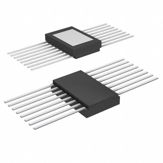
This multiplexer is available in a 16-lead ceramic flat package
(FLATPACK) and a 16-lead ceramic flat package with reverse
formed gullwing leads (FLATPACK_RF). Both packages are
designed for robustness at extreme temperatures and are
qualified for up to 1000 hours of operation at the maximum
temperature rating.
The ADG5298 is a member of a growing series of high temperature
qualified products offered by Analog Devices, Inc. For a complete
selection table of available high temperature products, see the
high temperature product list and qualification data available at
www.analog.com/hightemp.
Rev. 0
PRODUCT HIGHLIGHTS
1.
2.
3.
4.
5.
6.
7.
Trench Isolation Guards Against Latch-Up and Minimizes
Parasitic Leakage.
A dielectric trench separates the P channel and N channel
transistors to prevent latch-up even under severe overvoltage
conditions.
Achieved JESD78D Class II rating.
The ADG5298 was stressed to ±500 mA with a 10 ms pulse
at the maximum temperature of the device (210°C).
0.2 pC Charge Injection.
Dual-Supply Operation.
For applications where the analog signal is bipolar, the
ADG5298 can operate from dual supplies of up to ±22 V.
Single-Supply Operation.
For applications where the analog signal is unipolar, the
ADG5298 can operate from a single rail power supply of
up to 40 V.
3 V Logic-Compatible Digital Inputs.
VINH = 2.0 V, VINL = 0.8 V.
No Logic Power Supply (VL) Required.
Document Feedback
Information furnished by Analog Devices is believed to be accurate and reliable. However, no
responsibility is assumed by Analog Devices for its use, nor for any infringements of patents or other
rights of third parties that may result from its use. Specifications subject to change without notice. No
license is granted by implication or otherwise under any patent or patent rights of Analog Devices.
Trademarks and registered trademarks are the property of their respective owners.
One Technology Way, P.O. Box 9106, Norwood, MA 02062-9106, U.S.A.
Tel: 781.329.4700
©2016 Analog Devices, Inc. All rights reserved.
Technical Support
www.analog.com
�ADG5298
Data Sheet
TABLE OF CONTENTS
Features .............................................................................................. 1
Thermal Resistance .......................................................................7
Applications ....................................................................................... 1
ESD Caution...................................................................................7
General Description ......................................................................... 1
Pin Configurations and Function Descriptions ............................8
Functional Block Diagram .............................................................. 1
Typical Performance Characteristics ..............................................9
Product Highlights ........................................................................... 1
Test Circuits..................................................................................... 14
Revision History ............................................................................... 2
Terminology .................................................................................... 16
Specifications..................................................................................... 3
Theory of Operation ...................................................................... 17
±15 V Dual-Supply ....................................................................... 3
Trench Isolation .......................................................................... 17
±20 V Dual Supply ....................................................................... 4
Applications Information .............................................................. 18
12 V Single Supply ........................................................................ 5
Outline Dimensions ....................................................................... 19
36 V Single Supply ........................................................................ 6
Ordering Guide .......................................................................... 20
Continuous Current per Channel (Sx or D) ............................. 6
Absolute Maximum Ratings ............................................................ 7
REVISION HISTORY
9/2016—Revision 0: Initial Version
Rev. 0 | Page 2 of 20
�Data Sheet
ADG5298
SPECIFICATIONS
±15 V DUAL-SUPPLY
VDD = +15 V ± 10%, VSS = −15 V ± 10%, GND = 0 V, and −55°C ≤ TA ≤ +210°C, unless otherwise noted.
Table 1.
Parameter
ANALOG SWITCH
Analog Signal Range
On Resistance
Symbol 1
Test Conditions/Comments1
RON
On-Resistance Match Between Channels
On-Resistance Flatness
LEAKAGE CURRENTS
Source Off Leakage
Drain Off Leakage
Channel On Leakage
DIGITAL INPUTS
Input High Voltage
Input Low Voltage
Input Current
Digital Input Capacitance
DYNAMIC CHARACTERISTICS 3
Transition Time
ΔRON
RFLAT (ON)
Supply voltage (VS) = ±10 V, drain source
current (IDS) = −1 mA, see Figure 31; for
maximum RON, VDD = +13.5 V, VSS = −13.5 V
VS = ±10 V, IDS = −1 mA
VS = ±10 V, IDS = −1 mA
VDD = +16.5 V, VSS = −16.5 V
VS = ±10 V, VD = 10 V, see Figure 32
VS = ±10 V, VD = 10 V, see Figure 32
VS = VD = ±10 V, see Figure 30
1
2
3
Typ 2
Max
Unit
290
VDD
400
V
Ω
2.0
60
10
130
Ω
Ω
±0.005
±0.005
±0.01
+8
+60
+70
nA
nA
nA
0.8
+0.1
V
V
µA
pF
150
335
ns
125
160
55
275
275
ns
ns
ns
VSS
IS (off )
ID (off )
ID (on), IS (on)
VINH
VINL
IINL or IINH
CIN
tTRANSITION
On Time
Off Time
Break-Before-Make Time Delay
tON (EN)
tOFF (EN)
tD
Charge Injection
Off Isolation
Channel to Channel Crosstalk
−3 dB Bandwidth
Source Capacitance, Off
Drain Capacitance, Off
Source/Drain Capacitance, On
QINJ
POWER REQUIREMENTS
Supply Current
Positive
Negative
Ground Current
Supply Range
Min
CS (off )
CD (off )
CD (on), CS
(on)
−8
−60
−70
2.0
Input voltage (VIN) = ground voltage (VGND) or VDD
Load resistance (RL) = 300 Ω, load capacitance
(CL) = 35 pF, VS = 10 V, see Figure 36
RL = 300 Ω, CL = 35 pF, VS = 10 V, see Figure 38
RL = 300 Ω, CL = 35 pF, VS = 10 V, see Figure 38
RL = 300 Ω, CL = 35 pF, S1 voltage (VS1) =
S2 voltage (VS2) = 10 V, see Figure 37
VS = 0 V, RS = 0 Ω, CL = 1 nF, see Figure 39
RL = 50 Ω, CL = 5 pF, f = 1 MHz, see Figure 34
RL = 50 Ω, CL = 5 pF, f = 1 MHz, see Figure 33
RL = 50 Ω, CL = 5 pF, see Figure 35
VS = 0 V, frequency (f ) = 1 MHz
VS = 0 V, f = 1 MHz
VS = 0 V, f = 1 MHz
−0.1
25
+0.002
3
0.2
86
−80
110
2.9
34
37
pC
dB
dB
MHz
pF
pF
pF
VDD = +16.5 V, VSS = −16.5 V
IDD
ISS
IGND
VDD/VSS
Digital inputs = 0 V or 5 V, see Figure 28
Digital inputs = 0 V or 5 V, see Figure 29
Digital inputs = 0 V or 5 V
GND = 0 V
See the Terminology section.
TA = 25°C, except for the analog switch and power requirements values, where TA = 210°C.
Guaranteed by design, not subject to production test.
Rev. 0 | Page 3 of 20
60
10
60
±9
80
20
80
±22
µA
µA
µA
V
�ADG5298
Data Sheet
±20 V DUAL SUPPLY
VDD = +20 V ± 10%, VSS = −20 V ± 10%, GND = 0 V, and −55°C ≤ TA ≤ +210°C, unless otherwise noted.
Table 2.
Parameter
ANALOG SWITCH
Analog Signal Range
On Resistance
Symbol 1
Test Conditions/Comments1
RON
On-Resistance Match Between Channels
On-Resistance Flatness
LEAKAGE CURRENTS
Source Off Leakage
Drain Off Leakage
Channel On Leakage
DIGITAL INPUTS
Input High Voltage
Input Low Voltage
Input Current
Digital Input Capacitance
DYNAMIC CHARACTERISTICS 3
Transition Time
On Time
Off Time
Break-Before-Make Time Delay
ΔRON
RFLAT (ON)
VS = ±15 V, IDS = −1 mA, see Figure 31;
for maximum RON, VDD = +18 V, VSS = −18 V
VS = ±15 V, IDS = −1 mA
VS = ±15 V, IDS = −1 mA
VDD = +22 V, VSS = −22 V
VS = ±15 V, VD = 15 V, see Figure 32
VS = ±15 V, VD = 15 V, see Figure 32
VS = VD = ±15 V, see Figure 30
Charge Injection
Off Isolation
Channel to Channel Crosstalk
−3 dB Bandwidth
Source Capacitance, Off
Drain Capacitance, Off
Source/Drain Capacitance, On
POWER REQUIREMENTS
Supply Current
Positive
Negative
Ground Current
Supply Range
1
2
3
Min
Typ 2
Max
Unit
240
VDD
350
V
Ω
1.5
55
10
110
Ω
Ω
±0.005
±0.005
±0.01
+8
+60
+70
nA
nA
nA
0.8
+0.1
V
V
µA
pF
VSS
IS (off )
ID (off )
ID (on), IS (on)
VINH
VINL
IINL or IINH
CIN
tTRANSITION
tON (EN)
tOFF (EN)
tD
QINJ
CS (off )
CD (off )
CD (on), CS (on)
IDD
ISS
IGND
VDD/VSS
−8
−60
−70
2.0
VIN = VGND or VDD
RL = 300 Ω, CL = 35 pF, VS = 10 V, see Figure 36
RL = 300 Ω, CL = 35 pF, VS = 10 V, see Figure 38
RL = 300 Ω, CL = 35 pF, VS = 10 V, see Figure 38
RL = 300 Ω, CL = 35 pF, VS1 = VS2 = 10 V,
see Figure 37
VS = 0 V, RS = 0 Ω, CL = 1 nF, see Figure 39
RL = 50 Ω, CL = 5 pF, f = 1 MHz, see Figure 34
RL = 50 Ω, CL = 5 pF, f = 1 MHz, see Figure 33
RL = 50 Ω, CL = 5 pF, see Figure 35
VS = 0 V, f = 1 MHz
VS = 0 V, f = 1 MHz
VS = 0 V, f = 1 MHz
VDD = +22 V, VSS = −22 V
Digital inputs = 0 V or 5 V, see Figure 28
Digital inputs = 0 V or 5 V, see Figure 29
Digital inputs = 0 V or 5 V
GND = 0 V
See the Terminology section.
TA = 25°C, except for the analog switch and power requirements values, where TA = 210°C.
Guaranteed by design, not subject to production test.
Rev. 0 | Page 4 of 20
−0.1
20
+0.002
3
140
120
160
45
305
245
260
0.4
86
−80
121
2.8
33
36
60
10
60
±9
ns
ns
ns
ns
pC
dB
dB
MHz
pF
pF
pF
120
20
120
±22
µA
µA
µA
V
�Data Sheet
ADG5298
12 V SINGLE SUPPLY
VDD = 12 V ± 10%, VSS = 0 V, GND = 0 V, and −55°C ≤ TA ≤ +210°C, unless otherwise noted.
Table 3.
Parameter
ANALOG SWITCH
Analog Signal Range
On Resistance
Symbol 1
Test Conditions/Comments1
RON
On-Resistance Match Between Channels
On-Resistance Flatness
LEAKAGE CURRENTS
Source Off Leakage
Drain Off Leakage
Channel On Leakage
DIGITAL INPUTS
Input High Voltage
Input Low Voltage
Input Current
Digital Input Capacitance
DYNAMIC CHARACTERISTICS 3
Transition Time
On Time
Off Time
Break-Before-Make Time Delay
ΔRON
RFLAT (ON)
VS = 0 V to 10 V, IDS = −1 mA, see Figure 31;
for maximum RON, VDD = 10.8 V, VSS = 0 V
VS = 0 V to 10 V, IDS = −1 mA
VS = 0 V to 10 V, IDS = −1 mA
VDD = 13.2 V, VSS = 0 V
VS = 1 V/10 V, VD = 10 V/1 V, see Figure 32
VS = 1 V/10 V, VD = 10 V/1 V, see Figure 32
VS = VD = 1 V/10 V, see Figure 30
Charge Injection
Off Isolation
Channel to Channel Crosstalk
−3 dB Bandwidth
Source Capacitance, Off
Drain Capacitance, Off
Source/Drain Capacitance, On
POWER REQUIREMENTS
Supply Current
Positive
Negative
Ground Current
Supply Range
1
2
3
Min
Typ 2
Max
Unit
650
VDD
800
V
Ω
3
240
24
380
Ω
Ω
±0.005
±0.005
±0.01
+8
+60
+70
nA
nA
nA
0.8
+0.1
V
V
µA
pF
VSS
IS (off )
ID (off )
ID (on), IS (on)
VINH
VINL
IINL or IINH
CIN
tTRANSITION
tON (EN)
tOFF (EN)
tD
QINJ
CS (off )
CD (off )
CD (on), CS (on)
IDD
ISS
IGND
VDD/VSS
−8
−60
−70
2.0
VIN = VGND or VDD
RL = 300 Ω, CL = 35 pF, VS = 8 V, see Figure 36
RL = 300 Ω, CL = 35 pF, VS = 8 V, see Figure 38
RL = 300 Ω, CL = 35 pF, VS = 8 V, see Figure 38
RL = 300 Ω, CL = 35 pF, VS1 = VS2 = 8 V,
see Figure 37
VS = 6 V, RS = 0 Ω, CL = 1 nF, see Figure 39
RL = 50 Ω, CL = 5 pF, f = 1 MHz, see Figure 34
RL = 50 Ω, CL = 5 pF, f = 1 MHz, see Figure 33
RL = 50 Ω, CL = 5 pF, see Figure 35
VS = 6 V, f = 1 MHz
VS = 6 V, f = 1 MHz
VS = 6 V, f = 1 MHz
VDD = 13.2 V
Digital inputs = 0 V or 5 V, see Figure 28
Digital inputs = 0 V or 5 V, see Figure 29
Digital inputs = 0 V or 5 V
GND = 0 V, VSS = 0 V
See the Terminology section.
TA = 25°C, except for the analog switch and power requirements values, where TA = 210°C.
Guaranteed by design, not subject to production test.
Rev. 0 | Page 5 of 20
−0.1
40
+0.002
3
200
180
165
95
490
435
305
0.2
−86
−80
95
3.3
38
41
50
7.5
50
9
ns
ns
ns
ns
pC
dB
dB
MHz
pF
pF
pF
75
15
75
40
µA
µA
µA
V
�ADG5298
Data Sheet
36 V SINGLE SUPPLY
VDD = 36 V ± 10%, VSS = 0 V, GND = 0 V, and −55°C ≤ TA ≤ +210°C, unless otherwise noted.
Table 4.
Parameter
ANALOG SWITCH
Analog Signal Range
On Resistance
Symbol 1
Test Conditions/ Comments1
RON
On-Resistance Match Between Channels
On-Resistance Flatness
LEAKAGE CURRENTS
Source Off Leakage
Drain Off Leakage
Channel On Leakage
DIGITAL INPUTS
Input High Voltage
Input Low Voltage
Input Current
Digital Input Capacitance
DYNAMIC CHARACTERISTICS 3
Transition Time
On Time
Off Time
Break-Before-Make Time Delay
ΔRON
RFLAT (ON)
VS = 0 V to 30 V, IDS = −1 mA, see Figure 31;
for maximum RON, VDD = 32.4 V, VSS = 0 V
VS = 0 V to 30 V, IDS = −1 mA
VS = 0 V to 30 V, IDS = −1 mA
VDD = 13.2 V, VSS = 0 V
VS = 1 V/10 V, VD = 10 V/1 V, see Figure 32
VS = 1 V/10 V, VD = 10 V/1 V, see Figure 32
VS = VD = 1 V/10 V, see Figure 30
Charge Injection
Off Isolation
Channel to Channel Crosstalk
−3 dB Bandwidth
Source Capacitance, Off
Drain Capacitance, Off
Source/Drain Capacitance, On
POWER REQUIREMENTS
Supply Current
Positive
Negative
Ground Current
Supply Range
1
2
3
Min
Typ 2
Max
Unit
260
VDD
350
V
Ω
1.5
55
10
110
Ω
Ω
±0.005
±0.005
±0.01
+8
+60
+70
nA
nA
nA
0.8
+0.1
V
V
µA
pF
VSS
IS (off )
ID (off )
ID (on), IS (on)
VINH
VINL
IINL or IINH
CIN
tTRANSITION
tON (EN)
tOFF (EN)
tD
QINJ
CS (off )
CD (off )
CD (on), CS (on)
IDD
ISS
IGND
VDD/VSS
−8
−60
−70
2.0
VIN = VGND or VDD
−0.1
RL = 300 Ω, CL = 35 pF, VS = 18 V, see Figure 36
RL = 300 Ω, CL = 35 pF, VS = 18 V, see Figure 38
RL = 300 Ω, CL = 35 pF, VS = 18 V, see Figure 38
RL = 300 Ω, CL = 35 pF, VS1 = VS2 = 18 V,
see Figure 37
VS = 6 V, RS = 0 Ω, CL = 1 nF, see Figure 39
RL = 50 Ω, CL = 5 pF, f = 1 MHz, see Figure 34
RL = 50 Ω, CL = 5 pF, f = 1 MHz, see Figure 33
RL = 50 Ω, CL = 5 pF, see Figure 35
VS = 6 V, f = 1 MHz
VS = 6 V, f = 1 MHz
VS = 6 V, f = 1 MHz
VDD = 13.2 V
Digital inputs = 0 V or 5 V, see Figure 28
Digital inputs = 0 V or 5 V, see Figure 29
Digital inputs = 0 V or 5 V
GND = 0 V, VSS = 0 V
20
+0.002
3
170
150
180
55
320
265
265
0.3
−86
−80
105
2.7
32
35
80
10
80
9
pC
dB
dB
MHz
pF
pF
pF
155
20
155
40
See the Terminology section.
TA = 25°C, except for the analog switch and power requirements values, where TA = 210°C.
Guaranteed by design, not subject to production test.
CONTINUOUS CURRENT PER CHANNEL (Sx OR D)
Table 5.
Parameter
CONTINUOUS CURRENT (Sx OR D)
VDD = +15 V, VSS = −15 V
VDD = +20 V, VSS = −20 V
VDD = 12 V, VSS = 0 V
VDD = 36 V, VSS = 0 V
Test Conditions/Comments
θJA = 70 °C/W
Rev. 0 | Page 6 of 20
ns
ns
ns
ns
175°C
210°C
Unit
10
10
6
10
10
10
6
10
mA maximum
mA maximum
mA maximum
mA maximum
µA
µA
µA
V
�Data Sheet
ADG5298
ABSOLUTE MAXIMUM RATINGS
TA = 25°C, unless otherwise noted.
THERMAL RESISTANCE
Table 6.
Thermal performance is directly linked to printed circuit board
(PCB) design and operating environment. Careful attention to
PCB thermal design is required.
Parameter
VDD to VSS
VDD to GND
VSS to GND
Analog Inputs1
Digital Inputs1
Peak Current, Sx or D Pins
Continuous Current, Sx or D Pins2
Temperature Range
Junction Temperature
Reflow Soldering Peak Temperature,
Pb Free
1
2
Rating
48 V
−0.3 V to +48 V
+0.3 V to −48 V
VSS − 0.3 V to VDD + 0.3 V or
30 mA, whichever occurs first
VSS − 0.3 V to VDD + 0.3 V or
30 mA, whichever occurs first
31 mA (pulsed at 1 ms, 10%
duty cycle maximum)
Table 7. Thermal Resistance
Package Type
F-16-11
FR-16-11
1
θJC
22
10
Unit
°C/W
°C/W
Thermal impedance simulated values are based on JEDEC 2s2p thermal test
board. See JEDEC JESD51.
ESD CAUTION
Data + 5%
−55°C to +210°C
212°C
260°C (+ 0°C/− 5°C)
θJA
70
70
Overvoltages at the Ax, EN, Sx, or D pins are clamped by internal diodes.
Limit the current to the maximum ratings given.
See Table 5.
Stresses at or above those listed under Absolute Maximum
Ratings may cause permanent damage to the product. This is a
stress rating only; functional operation of the product at these
or any other conditions above those indicated in the operational
section of this specification is not implied. Operation beyond
the maximum operating conditions for extended periods may
affect product reliability.
Only one absolute maximum rating can be applied at any one
time.
Rev. 0 | Page 7 of 20
�ADG5298
Data Sheet
A0 1
16
A1
EN 2
15
A2
VSS 3
14
GND
13
VDD
S1 4
ADG5298
A1
A2
GND
VDD
S5
S6
S7
S8
S4 7
10
S7
D 8
9
S8
14872-002
TOP VIEW
S2 5 (Not to Scale) 12 S5
11 S6
S3 6
A0
EN
3 VSS
4 S1
5 S2
6 S3
7 S4
8 D
16
1
15
2
14
13
12
11
10
9
ADG5298
TOP VIEW
(Not to Scale)
14872-003
PIN CONFIGURATIONS AND FUNCTION DESCRIPTIONS
Figure 3. Reversed Formed FLATPACK Pin Configuration
Figure 2. FLATPACK Pin Configuration
Table 8. Pin Function Descriptions
Pin No.
1
2
Mnemonic
A0
EN
3
4
5
6
7
8
9
10
11
12
13
14
15
16
VSS
S1
S2
S3
S4
D
S8
S7
S6
S5
VDD
GND
A2
A1
Description
Logic Control Input 0.
Active High Digital Input. When low, the device is disabled and all switches are off. When high, the Ax logic inputs
determine the on switches.
Most Negative Power Supply Potential. In single-supply applications, this pin can be connected to ground.
Source Terminal 1. This pin can be an input or an output.
Source Terminal 2. This pin can be an input or an output.
Source Terminal 3. This pin can be an input or an output.
Source Terminal 4. This pin can be an input or an output.
Drain Terminal. This pin can be an input or an output.
Source Terminal 8. This pin can be an input or an output.
Source Terminal 7. This pin can be an input or an output.
Source Terminal 6. This pin can be an input or an output.
Source Terminal 5. This pin can be an input or an output.
Most Positive Power Supply Potential.
Ground (0 V) Reference.
Logic Control Input 2.
Logic Control Input 1.
Table 9. Truth Table
A2
X1
0
0
0
0
1
1
1
1
1
A1
X1
0
0
1
1
0
0
1
1
A0
X1
0
1
0
1
0
1
0
1
EN
0
1
1
1
1
1
1
1
1
X is don’t care.
Rev. 0 | Page 8 of 20
On Switch
None
S1
S2
S3
S4
S5
S6
S7
S8
�Data Sheet
ADG5298
TYPICAL PERFORMANCE CHARACTERISTICS
160
TA = 25°C
VDD = +18V
VSS = –18V
VDD = 32.4V
VSS = 0V
ON RESISTANCE (Ω)
120
100
80
VDD = +22V
VSS = –22V
VDD = +20V
VSS = –20V
60
100
80
40
40
20
20
15
20
25
Figure 4. On Resistance (RON) as a Function of VS, VD (±20 V Dual Supply)
VS, VD (V)
Figure 7. On Resistance (RON) as a Function of VS, VD (36 V Single Supply)
350
TA = 25°C
VDD = +9V
VSS = –9V
+210°C
+175°C
+125°C
+85°C
+25°C
–40°C
–55°C
VDD = +15V
VSS = –15V
300
ON RESISTANCE (Ω)
ON RESISTANCE (Ω)
200
150
100
VDD = +16.5V
VSS = –16.5V
VDD = +13.5V
VSS = –13.5V
VDD = +15V
VSS = –15V
14872-109
10
30.4
32.0
33.6
35.2
36.8
38.4
40.0
5
24.0
25.6
27.2
28.8
0
20.8
22.4
–5
16.0
17.6
19.2
–10
4.8
6.4
8.0
9.6
11.2
12.8
14.4
–15
VS, VD (V)
50
VDD = 39.6V
VSS = 0V
0
–20
0
1.6
0
–25
VDD = 36V
VSS = 0V
60
14872-106
ON RESISTANCE (Ω)
120
250
TA = 25°C
140
140
3.2
160
250
200
150
100
–15
–10
–5
0
5
10
15
20
VS, VD (V)
0
–15
14872-107
0
–20
VDD = 9V
VSS = 0V
400
–6
–3
ON RESISTANCE (Ω)
ON RESISTANCE (Ω)
VDD = 10.8V
VSS = 0V
300
250
200
VDD = 12V
VSS = 0V
150
VDD = 13.2V
VSS = 0V
3
6
9
12
15
+210°C
+175°C
+125°C
+85°C
+25°C
–40°C
–55°C
VDD = +20V
VSS = –20V
250
350
0
Figure 8. On Resistance (RON) as a Function of VS, VD for Various
Temperatures, ±15 V Dual Supply
300
TA = 25°C
–9
VS, VD (V)
Figure 5. On Resistance (RON) as a Function of VS, VD (±15 V Dual Supply)
450
–12
14872-008
50
200
150
100
100
13.2
12.6
11.4
12.0
10.8
9.6
10.2
9.0
0
–20
14872-108
VS, VD (V)
8.4
7.2
7.8
6.6
6.0
5.4
4.2
4.8
3.6
3.0
2.4
1.8
1.2
0
0.6
0
–15
–10
–5
0
5
10
15
20
VS, VD (V)
Figure 6. On Resistance (RON) as a Function of VS, VD (12 V Single Supply)
Rev. 0 | Page 9 of 20
Figure 9. On Resistance (RON) as a Function of VS, VD for Various
Temperatures, ±20 V Dual Supply
14872-009
50
50
�ADG5298
500
0
400
300
200
4
6
8
10
12
300
50
24
28
32
36
14872-011
16
20
VS, VD (V)
155
185
215
–15
–20
–25
IS (OFF) + –
ID (OFF) + –
IS (OFF) – +
ID (OFF) – +
IS, ID (ON) + +
IS, ID (ON) – –
–25
5
VDD = 12V
VSS = 0V
VBIAS = 1V, 10V
35
65
95
125
155
185
215
Figure 14. Leakage Current vs. Temperature, 12 V Single Supply
5
0
–5
–10
–15
IS (OFF) + –
ID (OFF) + –
IS (OFF) – +
ID (OFF) – +
IS , ID (ON) + +
IS , ID (ON) – –
–25
5
–10
–15
–20
–25
–30
IS (OFF) + –
ID (OFF) + –
IS (OFF) – +
ID (OFF) – +
IS, ID (ON) + +
IS, ID (ON) – –
–35
–40
35
65
95
125
155
185
215
TEMPERATURE (°C)
VDD = 36V
VSS = 0V
VBIAS = 1V, 30V
–45
–55
–25
5
35
65
95
125
155
185
215
TEMPERATURE (°C)
Figure 15. Leakage Current vs. Temperature, 36 V Single Supply
Figure 12. Leakage Currents vs. Temperature, ±15 V Dual Supply
Rev. 0 | Page 10 of 20
14872-022
LEAKAGE CURRENT (nA)
–5
14872-013
LEAKAGE CURRENT (nA)
125
TEMPERATURE (°C)
VDD = +15V
VSS = –15V
VBIAS = +10V, –10V
–25
–55
95
–10
–35
–55
Figure 11. On Resistance (RON) as a Function of VS, VD for Various
Temperatures, 36 V Single Supply
–20
65
–5
–30
VDD = 36V
VSS = 0V
12
35
TEMPERATURE (°C)
LEAKAGE CURRENT (nA)
ON RESISTANCE (Ω)
100
8
5
0
150
4
–25
5
200
0
IS (OFF) + –
ID (OFF) + –
IS (OFF) – +
ID (OFF) – +
IS , ID (ON) + +
IS , ID (ON) – –
Figure 13. Leakage Current vs. Temperature, ±20 V Dual Supply
+210°C
+175°C
+125°C
+85°C
+25°C
–40°C
–55°C
250
0
–30
–50
–55
Figure 10. On Resistance (RON) as a Function of VS, VD for Various
Temperatures, 12 V Single Supply
5
–20
14872-015
2
14872-010
0
VS, VD (V)
0
–10
–40
100
0
VDD = +20V
VSS = –20V
VBIAS = +15V, –15V
14872-014
600
ON RESISTANCE (Ω)
10
+210°C
+175°C
+125°C
+85°C
+25°C
–40°C
–55°C
VDD = 12V
VSS = 0V
LEAKAGE CURRENT (nA)
700
Data Sheet
�Data Sheet
ADG5298
0
–5
TA = 25°C
VDD = +15V
VSS = –15V
–60
–80
–7
–8
–9
–100
–10
–120
–11
100k
1M
10M
1G
100M
–12
100k
FREQUENCY (Hz)
10M
1G
Figure 19. Attenuation vs. Frequency, ±15 V Dual Supply
0
0
TA = 25°C
VDD = +15V
VSS = –15V
–20
TA = 25°C
VDD = +15V
VSS = –15V
–20
–40
ACPSRR (dB)
–40
–60
BETWEEN S1 AND S2
–80
BETWEEN S1 AND S8
NO DECOUPLING
CAPACITORS
–60
–80
–100
DECOUPLING
CAPACITORS
100k
1M
10M
1G
100M
–120
14872-119
FREQUENCY (Hz)
1M
10M
5
TA = 25°C
DEMUX (DRAIN TO SOURCE)
4
CHARGE INJECTION (pC)
30
VDD = +15V
VSS = –15V
25
VDD = +20V
VSS = –20V
VDD = +36V
VSS = 0V
15
10
0
10
VS (V)
20
30
VDD = +15V
VSS = –15V
2
1
VDD = +20V
VSS = –20V
0
–2
–20
14872-120
–10
TA = 25°C
MUX (SOURCE TO DRAIN)
3
–1
VDD = +12V
VSS = 0V
5
0
–20
100k
Figure 20. ACPSRR vs. Frequency, ±15 V Dual Supply
40
20
10k
FREQUENCY (Hz)
Figure 17. Crosstalk vs. Frequency, ±15 V Dual Supply
35
1k
VDD = +36V
VSS = 0V
VDD = +12V
VSS = 0V
–10
0
10
VS (V)
Figure 18. Charge Injection (QINJ) vs. Source Voltage (VS), Drain to Source
20
30
14872-123
–140
10k
14872-121
–100
–120
CHARGE INJECTION (pC)
100M
FREQUENCY (Hz)
Figure 16. Off Isolation vs. Frequency, ±15 V Dual Supply
CROSSTALK (dB)
1M
14872-122
ATTENUATION (dB)
–40
–140
10k
TA = 25°C
VDD = +15V
VSS = –15V
–6
14872-118
OFF ISOLATION (dB)
–20
Figure 21. Charge Injection (QINJ) vs. Source Voltage (VS), Source to Drain
Rev. 0 | Page 11 of 20
�ADG5298
4
CHARGE INJECTION (pC)
tTRANSITION TIME (ns)
300
250
200
150
100
3
2
1
0
50
10
60
110
160
210
TEMPERATURE (°C)
–1
–20
14872-012
0
–40
Figure 22. tTRANSITION Time vs. Temperature
CHARGE INJECTION (pC)
CAPACITANCE (pF)
SOURCE/DRAIN ON
DRAIN OFF
20
15
20
0.4
0.2
0
–0.2
–5
0
5
10
15
–0.6
14872-126
–10
VS (V)
Figure 23. Capacitance vs. Source Voltage(VS), ±15 V Dual Supply
VDD = 12V
VSS = 0V
0
2
4
6
8
10
12
VS (V)
Figure 26. Charge Injection as a Function of VS for Various Temperatures,
12 V Single Supply
4.0
+25°C
+175°C
+210°C
+25°C
+175°C
+210°C
3.5
3.0
2.0
CHARGE INJECTION (pC)
CHARGE INJECTION (pC)
10
+25°C
+175°C
+210°C
SOURCE OFF
2.5
5
–0.4
10
3.0
0
0.6
50
30
–5
0.8
60
40
–10
Figure 25. Charge Injection as a Function of VS for Various Temperatures, ±20
V Dual Supply
TA = 25°C
VDD = +15V
VSS = –15V
70
–15
VS (V)
80
0
–15
VDD = +20V
VSS = −20V
+25°C
+175°C
+210°C
14872-025
350
5
VDD = 12V, VSS = 0V
VDD = 36V, VSS = 0V
VDD = +15V, VSS = –15V
VDD = +20V, VSS = –20V
14872-026
400
Data Sheet
1.5
1.0
0.5
0
2.5
2.0
1.5
1.0
0.5
0
–10
–5
0
VS (V)
5
10
15
–1.0
14872-024
–1.0
–15
–0.5
VDD = +15V
VSS = −15V
Figure 24. Charge Injection as a Function of VS for Various Temperatures, ±15
V Dual Supply
VDD = 36V
VSS = 0V
0
5
10
15
20
VS (V)
25
30
35
14872-127
–0.5
Figure 27. Charge Injection as a Function of VS for Various Temperatures,
36 V Single Supply
Rev. 0 | Page 12 of 20
�Data Sheet
ADG5298
120
VDD
VDD
VDD
VDD
100
7
= 12V, VSS = 0V
= 36V, VSS = 0V
= +15V, VSS = –15V
= +20V, VSS = –20V
6
VDD
VDD
VDD
VDD
= 12V, VSS = 0V
= 36V, VSS = 0V
= +15V, VSS = –15V
= +20V, VSS = –20V
5
ISS (µA)
4
60
3
2
40
1
20
–25
5
35
65
95
125
TEMPERATURE (°C)
155
185
215
–1
–55
–25
5
35
65
95
125
TEMPERATURE (°C)
Figure 28. IDD vs Temperature
Figure 29. ISS vs Temperature
Rev. 0 | Page 13 of 20
155
185
215
14872-129
0
–55
0
14872-128
IDD (µA)
80
�ADG5298
Data Sheet
TEST CIRCUITS
VDD
VSS
0.1µF
NETWORK
ANALYZER
RL
50Ω
A
D
S2
S2
RL
50Ω
VS
VD
NC = NO CONNECT
14872-027
S8
VS
VSS
GND
CHANNEL-TO-CHANNEL CROSSTALK = 20 log
Figure 30. On Leakage
14872-029
D
VDD
S1
VOUT
ID (ON)
S1
NC
0.1µF
VOUT
VS
Figure 33. Channel-to-Channel Crosstalk
DD
VSS
VDD
VSS
0.1µF
NETWORK
ANALYZER
50Ω
Sx
50Ω
VS
V
D
GND
14872-028
IDS
RON = V ÷ IDS
S
RL
50Ω
OFF ISOLATION = 20 log
Figure 31. On Resistance
IS (OFF)
A
S1
D
VOUT
14872-030
Sx
VOUT
VS
Figure 34. Off Isolation
VDD
0.1µF
VSS
VDD
VSS
0.1µF
NETWORK
ANALYZER
Sx
ID (OFF)
50Ω
VS
A
D
GND
VD
VS
INSERTION LOSS = 20 log
Figure 32. Off Leakage
VOUT WITH SWITCH
VOUT WITHOUT SWITCH
Figure 35. −3 dB Bandwidth
Rev. 0 | Page 14 of 20
VOUT
14872-033
RL
50Ω
S8
14872-031
A
�Data Sheet
ADG5298
3V
ADDR ESS
DRIVE (VIN)
50%
50%
tR < 20ns
tF < 20ns
VDD
VSS
VDD
VSS
A0
0V
VIN
S1
A1
50Ω
A2
tTRANSITION
VS1
S2 TO S7
tTRANSITION
VS8
S8
90%
ADG5298
2.0V
OUTPUT
OUTPUT
D
EN
GND
300Ω
35pF
14872-034
10%
Figure 36. Address to Output Switching Times, tTRANSITION
3V
ADDRESS
DRIVE (VIN)
VDD
VSS
VDD
VSS
A0
VIN
0V
VS
S1
A1
50Ω
S2 TO S7
A2
S8
80%
ADG5298
80%
OUTPUT
2.0V
OUTPUT
D
EN
GND
300Ω
35pF
14872-035
tD
Figure 37. Break-Before-Make Time Delay, tD
3V
ENABLE
DRIVE (VIN)
50%
VDD
VSS
VDD
VSS
A0
50%
S1
A1
0V
S2 TO S8
A2
tON (EN)
ADG5298
tOFF (EN)
0.9V OUT
VIN
OUTPUT
D
EN
OUTPUT
VS
50Ω
300Ω
35pF
14872-036
GND
0.1V OUT
Figure 38. Enable Delay, tON (EN), tOFF (EN)
3V
VDD
VSS
VDD
VSS
A0
A1
A2
VOUT
RS
∆VOUT
QINJ = CL × ∆VOUT
ADG5298
Sx
D
EN
GND
VS
VIN
Figure 39. Charge Injection, QINJ
Rev. 0 | Page 15 of 20
VOUT
CL
1nF
14872-037
VIN
�ADG5298
Data Sheet
TERMINOLOGY
IDD
IDD represents the positive supply current.
CIN
CIN represents the digital input capacitance.
ISS
ISS represents the negative supply current.
tON (EN)
tON (EN) represents the delay time between the 50% and 90%
points of the digital input and switch on condition.
VD, VS
VD and VS represent the analog voltage on Terminal D and
Terminal Sx, respectively.
tOFF (EN)
tOFF (EN) represents the delay time between the 50% and 90%
points of the digital input and switch off condition.
RON
RON is the ohmic resistance between Terminal D and
Terminal Sx.
tTRANSITION
tTRANSITION represents the delay time between the 50% and 90%
points of the digital inputs and the switch on condition when
switching from one address state to another.
∆RON
∆RON represents the difference between the RON of any two
channels.
RFLAT (ON)
Flatness that is defined as the difference between the maximum
and minimum value of on resistance measured over the
specified analog signal range is represented by RFLAT (ON).
IS (Off)
IS (off) is the source leakage current with the switch off.
ID (Off)
ID (off) is the drain leakage current with the switch off.
ID (On), IS (On)
ID (on) and IS (on) represent the channel leakage currents with
the switch on.
VINL
VINL is the maximum input voltage for Logic 0.
Break-Before-Make Time Delay (tD)
tD represents the off time measured between the 80% point of
both switches when switching from one address state to
another.
Off Isolation
Off isolation is a measure of unwanted signal coupling through
an off channel.
Charge Injection
Charge injection is a measure of the glitch impulse transferred
from the digital input to the analog output during switching.
Crosstalk
Crosstalk is a measure of unwanted signal that is coupled
through from one channel to another as a result of parasitic
capacitance.
Bandwidth
Bandwidth is the frequency at which the output is attenuated
by −3 dB.
VINH
VINH is the minimum input voltage for Logic 1.
IINL, IINH
IINL and IINH represent the low and high input currents of the
digital inputs.
On Response
On response is the frequency response of the on switch.
CD (Off)
CD (off) represents the off switch drain capacitance, which is
measured with reference to ground.
CS (Off)
CS (off) represents the off switch source capacitance, which is
measured with reference to ground.
AC Power Supply Rejection Ratio (ACPSRR)
ACPSRR is a measure of the ability of a device to avoid coupling
noise and spurious signals that appear on the supply voltage pin
to the output of the switch. The dc voltage on the device is
modulated by a sine wave of 0.62 V p-p. The ratio of the amplitude
of signal on the output to the amplitude of the modulation is the
ACPSRR.
CD (On), CS (On)
CD (on) and CS (on) represent on switch capacitances, which are
measured with reference to ground.
Rev. 0 | Page 16 of 20
�Data Sheet
ADG5298
THEORY OF OPERATION
The ADG5298 is a latch-up proof, bidirectional, 8:1 CMOS
multiplexer that is designed to operate at very high temperatures.
The device is controlled by four parallel digital inputs (EN, A0,
A1, and A2). The EN input allows for the ADG5298 to be enabled
or disabled. When the ADG5298 is disabled, the source pins (S1
to S8) disconnect from the drain pin (D). When the ADG5298
is enabled, the address lines (A0, A1, and A2) can determine
which source pin (S1 to S8) is connected to the drain pin (D).
NMOS
PMOS
P WELL
N WELL
TRENCH ISOLATION
In junction isolation, the N well and P well of the PMOS and
NMOS transistors form a diode that is reverse biased under
normal operation. However, during overvoltage conditions, this
diode can become forward-biased. A silicon controlled rectifier
(SCR) type circuit is formed by the two transistors, causing a
significant amplification of the current that, in turn, leads to
latch-up. With trench isolation, this diode is removed, and the
result is a latch-up proof switch.
Rev. 0 | Page 17 of 20
TRENCH
BURIED OXIDE LAYER
HANDLE WAFER
Figure 40. Trench Isolation
14872-038
In the ADG5298, an insulating oxide layer (trench) is placed
between the negative channel metal-oxide semiconductor
(NMOS) and the positive channel metal-oxide semiconductor
(PMOS) transistors of each CMOS switch. Parasitic junctions,
which occur between the transistors in junction isolated switches,
are eliminated, and the result is a completely latch-up proof
switch that has minimal leakage over temperature.
�ADG5298
Data Sheet
APPLICATIONS INFORMATION
The ultralow capacitance and charge injection of this switch
makes it an ideal solution for data acquisition and sample-andhold applications, where low glitch and fast settling are required.
The ADG5298 can operate in a wide ambient temperature
range from −55°C to +210°C. Its wide range coupled with its
latch-up immune and low leakage features makes the ADG5298
perfect for use in harsh environments, such as downhole drilling
and avionics. The ADG5298 has achieved a JESD78D Class II
rating, handling stresses to ±500 mA with a 10 ms pulse at the
maximum operating temperature of the device (210°C).
Rev. 0 | Page 18 of 20
�Data Sheet
ADG5298
OUTLINE DIMENSIONS
7.01
6.86
6.71
8.89 MIN
25.65
25.40
25.15
5.23
5.08
4.93
1.34
1.27
1.20
1
16
10.36
10.16
9.96
7.40
7.24
7.09
TOP VIEW
R 0.32
BSC
0.70 REF
0.20 MIN
SIDE VIEW
0.66 MIN
PKG-004164/4875
0.89
BSC
BOTTOM VIEW
2.32
2.11
1.90
END VIEW
0.152
0.127
0.102
1.02
MIN
0.48
0.43
0.38
9
04-27-2016-A
8
Figure 41. 16-Lead Ceramic Flat Package [FLATPACK]
(F-16-1)
Dimensions shown in millimeters
10.36
10.16
9.96
7.40
7.24
7.09
8
1
5.23
5.08
4.93
7.01
6.86
6.71
12.446
REF
9
BOTTOM VIEW
2.32
2.11
1.90
0.66 MIN
SIDE VIEW
3.02
2.74
2.46
PKG-004875
SEATING
PLANE
4.978
4.826
4.673
0.254
0.203
0.152
1.34
1.27
1.20
0.48
0.43
0.38
0.432
0.381
0.330
0.152
0.127
0.102
0.254
0.203
0.152
END VIEW
Figure 42. 16-Lead Ceramic Flat Package with Reverse Formed Gullwing Leads [FLATPACK_RF]
Cavity Down
(FR-16-1)
Dimensions shown in millimeters
Rev. 0 | Page 19 of 20
1.524
1.397
1.270
1.524
1.397
1.270
06-24-2015-A
16
�ADG5298
Data Sheet
ORDERING GUIDE
Model 1
ADG5298HFZ
ADG5298HFRZ
EVAL-ADG5298EB1Z
1
Temperature Range
−55°C to +210°C
−55°C to +210°C
Package Description
16-Lead Ceramic Flat Package [FLATPACK]
16-Lead Ceramic Flat Package with Reverse Formed Gullwing Leads [FLATPACK_RF]
Evaluation Board
Z = RoHS Compliant Part.
©2016 Analog Devices, Inc. All rights reserved. Trademarks and
registered trademarks are the property of their respective owners.
D14872-0-9/16(0)
Rev. 0 | Page 20 of 20
Package
Option
F-16-1
FR-16-1
�


 工商网监
湘ICP备2023018690号
工商网监
湘ICP备2023018690号
