FEATURES
FUNCTIONAL BLOCK DIAGRAM
D1P D1N D2P D2N
TEMP
SENSOR
REFIN REFOUT REFGND SDA SCL A1
VREF
INTERNAL
DIODE
MUX
Complete supervisory and sequencing solution for up to
10 supplies
10 supply fault detectors enable supervision of supplies to
2.5V)
Figure 33. Configuration Update Flow Diagram
UPDATING THE SEQUENCING ENGINE
Sequencing engine (SE) functions are not updated in the same
way as regular configuration latches. The SE has its own dedicated
512-byte nonvolatile, electrically erasable, programmable, readonly memory (EEPROM) for storing state definitions, providing
63 individual states, each with a 64-bit word (one state is reserved).
At power-up, the first state is loaded from the SE EEPROM into
the engine itself. When the conditions of this state are met, the
next state is loaded from the EEPROM into the engine, and so
on. The loading of each new state takes approximately 10 μs.
To alter a state, the required changes must be made directly to
the EEPROM. RAM for each state does not exist. The relevant
alterations must be made to the 64-bit word, which is then
uploaded directly to the EEPROM.
INTERNAL REGISTERS
The ADM1063 contains a large number of data registers. The
principal registers are the address pointer register and the
configuration registers.
The major differences between the EEPROM and other
registers are as follows:
The first EEPROM is split into 16 (0 to 15) pages of 32 bytes each.
Page 0 to Page 6, starting at Address 0xF800, hold the configuration
data for the applications on the ADM1063 (such as the SFDs and
PDOs). These EEPROM addresses are the same as the RAM
register addresses, prefixed by F8. Page 7 is reserved. Page 8 to
Page 15 are for customer use.
Data can be downloaded from the EEPROM to the RAM in one
of the following ways:
Address Pointer Register
The address pointer register contains the address that selects
one of the other internal registers. When writing to the
ADM1063, the first byte of data is always a register address that
is written to the address pointer register.
An EEPROM location must be blank before it can be
written to. If it contains data, the data must first be erased.
Writing to the EEPROM is slower than writing to the RAM.
Writing to the EEPROM should be restricted because it has a
limited write/cycle life of typically 10,000 write operations,
due to the usual EEPROM wear-out mechanisms.
At power-up, when Page 0 to Page 6 are downloaded.
By setting Bit 0 of the UDOWNLD register (0xD8), which
performs a user download of Page 0 to Page 6.
SERIAL BUS INTERFACE
The configuration registers provide control and configuration
for various operating parameters of the ADM1063.
The ADM1063 is controlled via the serial system management
bus (SMBus) and is connected to this bus as a slave device,
under the control of a master device. It takes approximately
1 ms after power-up for the ADM1063 to download from its
EEPROM. Therefore, access to the ADM1063 is restricted until
the download is complete.
EEPROM
Identifying the ADM1063 on the SMBus
The ADM1063 has two 512-byte cells of nonvolatile EEPROM
from Register Address 0xF800 to Register Address 0xFBFF. The
EEPROM is used for permanent storage of data that is not lost
when the ADM1063 is powered down. One EEPROM cell contains
the configuration data of the device; the other contains the state
definitions for the SE. Although referred to as read-only memory,
the EEPROM can be written to, as well as read from, using the
serial bus in exactly the same way as the other registers.
The ADM1063 has a 7-bit serial bus slave address (see Table 11).
The device is powered up with a default serial bus address.
The five MSBs of the address are set to 00111, and the two LSBs
are determined by the logical states of Pin A1 and Pin A0. This
allows the connection of four ADM1063 devices to one SMBus.
Configuration Registers
Table 11. Serial Bus Slave Address
A1 Pin
Low
Low
High
High
1
A0 Pin
Low
High
Low
High
Hex Address
0x38
0x3Ah
0x3Ch
0x3Eh
7-Bit Address1
0011100x
0011101x
0011110x
0011111x
x = Read/Write bit. The address is shown only as the first 7 MSBs.
Rev. D | Page 27 of 33
�ADM1063
Data Sheet
The device also has several identification registers (read-only)
that can be read across the SMBus. Table 12 lists these registers
with their values and functions.
Table 12. Identification Register Values and Functions
Name
MANID
REVID
MARK1
MARK2
Address
0xF4
0xF5
0xF6
0xF7
Value
0x41
0x02
0x00
0x00
Function
Manufacturer ID for Analog Devices
Silicon revision
Software brand
Software brand
General SMBus Timing
Figure 34, Figure 35, and Figure 36 are timing diagrams for
general read and write operations using the SMBus. The SMBus
specification defines specific conditions for different types of
read and write operations, which are discussed in the Write
Operations and Read Operations sections.
The general SMBus protocol operates as follows:
Step 1
The master initiates data transfer by establishing a start condition,
defined as a high-to-low transition on the serial data (SDA) line
while the serial clock line (SCL) remains high. This indicates that a
data stream follows. All slave peripherals connected to the serial
bus respond to the start condition and shift in the next eight bits,
consisting of a 7-bit slave address (MSB first) plus an R/W bit.
This bit determines the direction of the data transfer, that is,
whether data is written to or read from the slave device (0 = write,
1 = read).
The peripheral whose address corresponds to the transmitted
address responds by pulling the data line low during the low
period before the ninth clock pulse, known as the acknowledge
bit, and by holding it low during the high period of this clock pulse.
All other devices on the bus remain idle while the selected device
waits for data to be read from or written to it. If the R/W bit is a 0,
the master writes to the slave device. If the R/W bit is a 1, the
master reads from the slave device.
Step 2
Data is sent over the serial bus in sequences of nine clock pulses:
eight bits of data followed by an acknowledge bit from the slave
device. Data transitions on the data line must occur during the low
period of the clock signal and remain stable during the high period
because a low-to-high transition when the clock is high could be
interpreted as a stop signal. If the operation is a write operation,
the first data byte after the slave address is a command byte. This
command byte tells the slave device what to expect next. It may be
an instruction telling the slave device to expect a block write, or
it may be a register address that tells the slave where subsequent
data is to be written. Because data can flow in only one direction,
as defined by the R/W bit, sending a command to a slave device
during a read operation is not possible. Before a read operation,
it may be necessary to perform a write operation to tell the slave
what sort of read operation to expect and/or the address from
which data is to be read.
Step 3
When all data bytes have been read or written, stop conditions
are established. In write mode, the master pulls the data line high
during the 10th clock pulse to assert a stop condition. In read
mode, the master device releases the SDA line during the low
period before the ninth clock pulse, but the slave device does
not pull it low. This is known as a no acknowledge. The master
then takes the data line low during the low period before the
10th clock pulse and then high during the 10th clock pulse to
assert a stop condition.
SCL Held Low Timeout
If the bus master holds the SCL low for a time that is a multiple
of approximately 30 ms, the ADM1063 bus interface may timeout.
If this timeout happens, the in progress transaction is NACKed,
and the transaction must be repeated. This behavior is only seen
if the I2C bus master is interrupted midtransaction by a higher
priority task that delays completion of the transaction.
False Start Detection
The data hold time specification defines the time that data must
be valid on the SDA line, following an SCL falling edge. If there
are multiple ADM1063 devices on the same bus, one of the
ADM1063 devices may see the SCL/SDA transition due to an
acknowledge (ACK) from a different device as a start condition
because of internal timing skew, which for most transactions,
this is not an issue. In a case where the data appearing on the
bus after the false start is detected happens to match the address
of another ADM1063 on the bus, that device may incorrectly ACK.
A bus master may see this ACK as another bus master talking
on the bus, halt the bus transaction, and not produce any more
clocks on the SCL. As a result, the ADM1063 device that
incorrectly ACKed continues to hold down the SDA line low.
To retry the halted bus transaction, the bus master performs a
clock flush on the SCL by sending a series of up to 16 clock pulses.
The clock flush forces the ADM1063 to release the SDA line.
Rev. D | Page 28 of 33
�Data Sheet
ADM1063
1
9
1
9
SCL
0
1
1
1
A1
A0
D7
R/W
D6
D5
D4
D3
D2
D1
ACK. BY
SLAVE
START BY
MASTER
FRAME 1
SLAVE ADDRESS
FRAME 2
COMMAND CODE
1
SCL
(CONTINUED)
SDA
(CONTINUED)
9
D7
D6
D5
D4
D3
D0
ACK. BY
SLAVE
D2
D1
1
D7
D0
9
D6
D5
ACK. BY
SLAVE
FRAME 3
DATA BYTE
D4
D3
D2
D1
D0
ACK. BY
SLAVE
FRAME N
DATA BYTE
STOP
BY
MASTER
04632-036
0
SDA
Figure 34. General SMBus Write Timing Diagram
1
9
1
9
SCL
0
1
1
1
A1
A0 R/W
D7
D6
D5
D4
D3
D2
D1
ACK. BY
SLAVE
START BY
MASTER
1
SCL
(CONTINUED)
SDA
(CONTINUED)
D7
FRAME 1
SLAVE ADDRESS
D6
D5
D4
D3
9
D2
FRAME 3
DATA BYTE
D1
D0
ACK. BY
MASTER
D0
1
D7
FRAME 2
DATA BYTE
D6
D5
ACK. BY
MASTER
D4
9
D3
D2
FRAME N
DATA BYTE
D1
D0
NO ACK.
STOP
BY
MASTER
Figure 35. General SMBus Read Timing Diagram
tR
tF
t HD; STA
t LO W
SCL
t HI G H
t HD; STA
t HD; DAT
t SU; STA
t SU; STO
t SU; DAT
t BUF
P
S
S
Figure 36. Serial Bus Timing Diagram
Rev. D | Page 29 of 33
P
04632-038
SDA
04632-037
0
SDA
�ADM1063
Data Sheet
SMBus PROTOCOLS FOR RAM AND EEPROM
In the ADM1063, the send byte protocol is used for two purposes:
The ADM1063 contains volatile registers (RAM) and nonvolatile registers (EEPROM). User RAM occupies Address 0x00 to
Address 0xDF; the EEPROM occupies Address 0xF800 to
Address 0xFBFF.
S
WRITE OPERATIONS
The SMBus specification defines several protocols for different
types of read and write operations. The following abbreviations
are used in Figure 37 to Figure 45:
S = Start
P = Stop
R = Read
W = Write
A = Acknowledge
A = No acknowledge
In a send byte operation, the master device sends a single
command byte to a slave device, as follows:
4.
5.
6.
5
6
A
A
P
To erase a page of EEPROM memory. EEPROM memory
can be written to only if it is unprogrammed. Before writing
to one or more EEPROM memory locations that are already
programmed, the page(s) containing those locations must
first be erased. EEPROM memory is erased by writing a
command byte.
The master sends a command code telling the slave device
to erase the page. The ADM1063 command code for a page
erasure is 0xFE (1111 1110). Note that for a page erasure to
take place, the page address must be given in the previous
write word transaction (see the Write Byte/Word section).
In addition, Bit 2 in the UPDCFG register (Address 0x90)
must be set to 1.
1
2
S
SLAVE
ADDRESS
W
3
4
5
6
A
COMMAND
BYTE
(0xFE)
A
P
As soon as the ADM1063 receives the command byte, page
erasure begins. The master device can send a stop command
as soon as it sends the command byte. Page erasure takes
approximately 20 ms. If the ADM1063 is accessed before
erasure is complete, it responds with a no acknowledge
(NACK).
Send Byte
3.
W
4
RAM
ADDRESS
(0x00 TO 0xDF)
Figure 38. EEPROM Page Erasure
The ADM1063 uses the following SMBus write protocols.
1.
2.
SLAVE
ADDRESS
3
Figure 37. Setting a RAM Address for Subsequent Read
Page erasure is enabled by setting Bit 2 in the UPDCFG register
(Address 0x90) to 1. If this bit is not set, page erasure cannot
occur, even if the command byte (0xFE) is programmed across
the SMBus.
2
04632-039
1
04632-040
Data can be written to and read from both the RAM and the
EEPROM as single data bytes. Data can be written only to
unprogrammed EEPROM locations. To write new data to a
programmed location, the location contents must first be erased.
EEPROM erasure cannot be done at the byte level. The EEPROM
is arranged as 32 pages of 32 bytes each, and an entire page
must be erased.
To write a register address to the RAM for a subsequent single
byte read from the same address, or for a block read or a
block write starting at that address, as shown in Figure 37.
The master device asserts a start condition on SDA.
The master sends the 7-bit slave address followed by the
write bit (low).
The addressed slave device asserts an acknowledge (ACK)
on SDA.
The master sends a command code.
The slave asserts an ACK on SDA.
The master asserts a stop condition on SDA, and the
transaction ends.
Rev. D | Page 30 of 33
�Data Sheet
ADM1063
Write Byte/Word
Block Write
In a write byte/word operation, the master device sends a
command byte and one or two data bytes to the slave device,
as follows:
In a block write operation, the master device writes a block of
data to a slave device. The start address for a block write must
have been set previously. In the ADM1063, a send byte operation sets a RAM address, and a write byte/word operation sets
an EEPROM address, as follows:
The master device asserts a start condition on SDA.
The master sends the 7-bit slave address followed by the
write bit (low).
3. The addressed slave device asserts an ACK on SDA.
4. The master sends a command code.
5. The slave asserts an ACK on SDA.
6. The master sends a data byte.
7. The slave asserts an ACK on SDA.
8. The master sends a data byte or asserts a stop condition.
9. The slave asserts an ACK on SDA.
10. The master asserts a stop condition on SDA to end
the transaction.
In the ADM1063, the write byte/word protocol is used for
three purposes:
To write a single byte of data to the RAM. In this case, the
command byte is RAM Address 0x00 to RAM Address 0xDF,
and the only data byte is the actual data, as shown in
Figure 39.
1
2
3
SLAVE W A
S ADDRESS
4
5
6
7 8
RAM
ADDRESS
A DATA A P
(0x00 TO 0xDF)
The master device asserts a start condition on SDA.
The master sends the 7-bit slave address followed by
the write bit (low).
3. The addressed slave device asserts an ACK on SDA.
4. The master sends a command code that tells the slave
device to expect a block write. The ADM1063 command
code for a block write is 0xFC (1111 1100).
5. The slave asserts an ACK on SDA.
6. The master sends a data byte that tells the slave device how
many data bytes are being sent. The SMBus specification
allows a maximum of 32 data bytes in a block write.
7. The slave asserts an ACK on SDA.
8. The master sends N data bytes.
9. The slave asserts an ACK on SDA after each data byte.
10. The master asserts a stop condition on SDA to end
the transaction.
1
To set up a 2-byte EEPROM address for a subsequent
read, write, block read, block write, or page erase. In this
case, the command byte is the high byte of EEPROM
Address 0xF8 to EEPROM Address 0xFB. The only data
byte is the low byte of the EEPROM address, as shown in
Figure 40.
2
3
SLAVE
S ADDRESS W A
4
5
6
7 8
EEPROM
EEPROM
ADDRESS
ADDRESS
A
A P
HIGH BYTE
LOW BYTE
(0xF8 TO 0xFB)
(0x00 TO 0xFF)
04632-042
1
Figure 40. Setting an EEPROM Address
Because a page consists of 32 bytes, only the three MSBs of
the address low byte are important for page erasure. The
lower five bits of the EEPROM address low byte specify the
addresses within a page and are ignored during an erase
operation.
2
3
4
5
6
7
8
5
6
7
8
9
10
9 10
EEPROM
EEPROM
SLAVE
ADDRESS
ADDRESS
S
W A
A
A DATA A P
ADDRESS
HIGH BYTE
LOW BYTE
(0xF8 TO 0xFB)
(0x00 TO 0xFF)
There must be at least N locations from the start address to
the highest EEPROM address (0xFBFF) to avoid writing to
invalid addresses.
An address crosses a page boundary. In this case, both
pages must be erased before programming.
Note that the ADM1063 features a clock extend function for
writes to EEPROM. Programming an EEPROM byte takes
approximately 250 μs, which limits the SMBus clock for
repeated or block write operations. The ADM1063 pulls SCL
low and extends the clock pulse when it cannot accept any
more data.
To write a single byte of data to the EEPROM. In this case,
the command byte is the high byte of EEPROM Address 0xF8
to EEPROM Address 0xFB. The first data byte is the low
byte of the EEPROM address, and the second data byte is
the actual data, as shown in Figure 41.
1
4
Unlike some EEPROM devices that limit block writes to within
a page boundary, there is no limitation on the start address
when performing a block write to EEPROM, except when
04632-043
3
Figure 42. Block Write to the EEPROM or RAM
Figure 39. Single Byte Write to the RAM
2
S SLAVE
W A COMMAND 0xFC A BYTE A DATA A DATA A DATA A P
ADDRESS
(BLOCK WRITE)
COUNT
1
2
N
04632-041
1.
2.
04632-044
1.
2.
Figure 41. Single Byte Write to the EEPROM
Rev. D | Page 31 of 33
�ADM1063
Data Sheet
10.
11.
12.
13.
The ADM1063 uses the following SMBus read protocols.
Receive Byte
In a receive byte operation, the master device receives a single
byte from a slave device, as follows:
3.
4.
5.
6.
The master device asserts a start condition on SDA.
The master sends the 7-bit slave address followed by the
read bit (high).
The addressed slave device asserts an ACK on SDA.
The master receives a data byte.
The master asserts a NACK on SDA.
The master asserts a stop condition on SDA, and the
transaction ends.
S
R
3
4
5
6
A
DATA
A
P
04632-045
2
SLAVE
ADDRESS
Figure 43. Single Byte Read from the EEPROM or RAM
Block Read
In a block read operation, the master device reads a block of
data from a slave device. The start address for a block read must
have been set previously. In the ADM1063, this is done by a
send byte operation to set a RAM address or a write byte/word
operation to set an EEPROM address. The block read operation
itself consists of a send byte operation that sends a block read
command to the slave, immediately followed by a repeated start
and a read operation that reads out multiple data bytes, as follows:
1.
2.
3.
4.
5.
6.
7.
8.
9.
3
4
5 6
7
8
9
10
11
12
SLAVE
COMMAND 0xFD
SLAVE
BYTE
DATA
R A
A
A
W A
A S
ADDRESS
(BLOCK READ)
ADDRESS
COUNT
1
13
DATA A
32
P
Figure 44. Block Read from the EEPROM or RAM
Error Correction
The ADM1063 provides the option of issuing a packet error
correction (PEC) byte after a write to the RAM, a write to the
EEPROM, a block write to the RAM/EEPROM, or a block read
from the RAM/ EEPROM. This option enables the user to verify
that the data received by or sent from the ADM1063 is correct.
The PEC byte is an optional byte sent after the last data byte has
been written to or read from the ADM1063. The protocol is the
same as for a block read for Step 1 to Step 12 and then proceeds
as follows:
In the ADM1063, the receive byte protocol is used to read a
single byte of data from a RAM or EEPROM location whose
address has previously been set by a send byte or write
byte/word operation, as shown in Figure 43.
1
S
2
The master device asserts a start condition on SDA.
The master sends the 7-bit slave address followed by the
write bit (low).
The addressed slave device asserts an ACK on SDA.
The master sends a command code that tells the slave
device to expect a block read. The ADM1063 command
code for a block read is 0xFD (1111 1101).
The slave asserts an ACK on SDA.
The master asserts a repeat start condition on SDA.
The master sends the 7-bit slave address followed by the
read bit (high).
The slave asserts an ACK on SDA.
The ADM1063 sends a byte-count data byte that tells the
master how many data bytes to expect. The ADM1063
always returns 32 data bytes (0x20), which is the maximum
allowed by the SMBus Version 1.1 specification.
13. The ADM1063 issues a PEC byte to the master. The master
checks the PEC byte and issues another block read if the
PEC byte is incorrect.
14. A NACK is generated after the PEC byte to signal the end
of the read.
15. The master asserts a stop condition on SDA to end
the transaction.
Note that the PEC byte is calculated using CRC-8. The frame
check sequence (FCS) conforms to CRC-8 by the polynomial
C(x) = x8 + x2 + x1 + 1
See the SMBus Version 1.1 specification for details.
An example of a block read with the optional PEC byte is shown
in Figure 45.
1
S
2
3
4
5 6
7
8
9
10
11
12
SLAVE
W A COMMAND 0xFD A S SLAVE R A BYTE A DATA A
ADDRESS
(BLOCK READ)
ADDRESS
COUNT
1
Rev. D | Page 32 of 33
13 14 15
DATA
32
A PEC A P
Figure 45. Block Read from the EEPROM or RAM with PEC
04632-047
1.
2.
1
The master asserts an ACK on SDA.
The master receives 32 data bytes.
The master asserts an ACK on SDA after each data byte.
The master asserts a stop condition on SDA to end
the transaction.
04632-046
READ OPERATIONS
�Data Sheet
ADM1063
OUTLINE DIMENSIONS
6.10
6.00 SQ
5.90
31
1
0.50
BSC
TOP VIEW
0.80
0.75
0.70
10
11
20
BOTTOM VIEW
0.25 MIN
FOR PROPER CONNECTION OF
THE EXPOSED PAD, REFER TO
THE PIN CONFIGURATION AND
FUNCTION DESCRIPTIONS
SECTION OF THIS DATA SHEET.
0.05 MAX
0.02 NOM
COPLANARITY
0.08
0.20 REF
SEATING
PLANE
4.25
4.10 SQ
3.95
EXPOSED
PAD
21
0.45
0.40
0.35
PIN 1
INDICATOR
40
30
05-06-2011-A
PIN 1
INDICATOR
0.30
0.25
0.18
COMPLIANT TO JEDEC STANDARDS MO-220-WJJD.
Figure 46. 40-Lead Lead Frame Chip Scale Package [LFCSP_WQ]
6 mm × 6 mm Body, Very Very Thin Quad
(CP-40-9)
Dimensions shown in millimeters
0.75
0.60
0.45
1.20
MAX
9.00
BSC SQ
37
36
48
1
PIN 1
1.05
1.00
0.95
0.15
0.05
SEATING
PLANE
0.20
0.09
7°
3.5°
0°
0.08 MAX
COPLANARITY
7.00
BSC SQ
TOP VIEW
0° MIN
(PINS DOWN)
12
13
25
24
VIEW A
VIEW A
0.50
0.27
BSC
0.22
LEAD PITCH
0.17
ROTATED 90° CCW
COMPLIANT TO JEDEC STANDARDS MS-026ABC
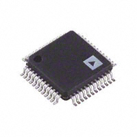
Figure 47. 48-Lead Thin Plastic Quad Flat Package [TQFP]
(SU-48)
Dimensions shown in millimeters
ORDERING GUIDE
Model1
ADM1063ACPZ
ADM1063ACPZ-REEL7
ADM1063ASUZ
ADM1063ASUZ-REEL7
EVAL-ADM1063TQEBZ
1
Temperature Range
−40°C to +85°C
−40°C to +85°C
−40°C to +85°C
−40°C to +85°C
Package Description
40-Lead Lead Frame Chip Scale Package [LFCSP_WQ]
40-Lead Lead Frame Chip Scale Package [LFCSP_WQ]
48-Lead Thin Plastic Quad Flat Package [TQFP]
48-Lead Thin Plastic Quad Flat Package [TQFP]
Evaluation Kit (TQFP Version)
Z = RoHS Compliant Part.
I2C refers to a communications protocol originally developed by Philips Semiconductors (now NXP Semiconductors).
©2005–2015 Analog Devices, Inc. All rights reserved. Trademarks and
registered trademarks are the property of their respective owners.
D04632-0-1/15(D)
Rev. D | Page 33 of 33
Package Option
CP-40-9
CP-40-9
SU-48
SU-48
�


 工商网监
湘ICP备2023018690号
工商网监
湘ICP备2023018690号
