Multirate 155 Mbps/622 Mbps/1244 Mbps/1250 Mbps
Burst Mode Clock and Data Recovery IC with Deserializer
ADN2855
Data Sheet
FEATURES
GENERAL DESCRIPTION
Serial data input
155.52 Mbps/622.08 Mbps/1244.16 Mbps/1250.00 Mbps
12-bit acquisition time
4-bit parallel LVDS output interface
Patented dual-loop clock recovery architecture
Integrated PRBS generator
Byte rate reference clock
Loss-of-lock indicator
Supports double data rate (DDR)-compatible FPGA
I2C interface to access optional features
Single-supply operation: 3.3 V
Power
670 mW typical in serial output mode
825 mW typical in deserializer mode
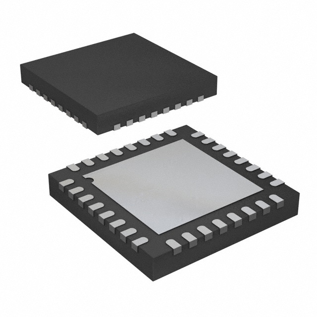
5 mm × 5 mm, 32-lead LFCSP
The ADN2855 is a burst mode clock and data recovery IC
designed for GPON/BPON/GEPON optical line terminal (OLT)
receiver applications. The part can operate at 155.52 Mbps,
622.08 Mbps, 1244.16 Mbps, or 1250.00 Mbps data rates, selectable
via the I2C interface.
The ADN2855 frequency locks to the OLT reference clock and
aligns to the input data within 12 bits of the start of the preamble.
The device provides a full rate or an optional half rate output
clock for a double data rate (DDR) interface to an FPGA or
digital ASIC.
All specifications are quoted for −40°C to +85°C ambient temperature, unless otherwise noted. The ADN2855 is available in a
compact 5 mm × 5 mm, 32-lead chip scale package.
APPLICATIONS
Passive optical networks
GPON/BPON/GEPON OLT receivers
FUNCTIONAL BLOCK DIAGRAM
REFCLKP,
REFCLKN
DATAV
CF1
CF2
VCC
VEE
ADN2855
RESET
FREQUENCY/
LOCK
DETECT
LOOP
FILTER
PHASE
DETECT
LOOP
FILTER
PIN
NIN
CML INPUT
BUFFER
PHASE
SHIFTER
VCO
DATA
RE-TIMING
2
I2C
DIVIDER
DESERIALIZER
SDA
SCK
SQUELCH
4×2
CLKOUTP,
CLKOUTN
06660-001
DATxP,
DATxN
2
Figure 1.
Rev. B
Document Feedback
Information furnished by Analog Devices is believed to be accurate and reliable. However, no
responsibility is assumed by Analog Devices for its use, nor for any infringements of patents or other
rights of third parties that may result from its use. Specifications subject to change without notice. No
license is granted by implication or otherwise under any patent or patent rights of Analog Devices.
Trademarks and registered trademarks are the property of their respective owners.
One Technology Way, P.O. Box 9106, Norwood, MA 02062-9106, U.S.A.
Tel: 781.329.4700 ©2009–2017 Analog Devices, Inc. All rights reserved.
Technical Support
www.analog.com
�ADN2855
Data Sheet
TABLE OF CONTENTS
Features .............................................................................................. 1
I2C Interface Timing and Internal Register Description ..............9
Applications ....................................................................................... 1
Theory of Operation ...................................................................... 11
General Description ......................................................................... 1
Functional Description .................................................................. 12
Functional Block Diagram .............................................................. 1
Frequency Acquisition ............................................................... 12
Revision History ............................................................................... 2
Squelch Mode ............................................................................. 12
Specifications..................................................................................... 3
I2C Interface ................................................................................ 12
Jitter Specifications ....................................................................... 3
Reference Clock .......................................................................... 13
Output and Timing Specifications ............................................. 4
Output Modes ............................................................................. 14
Timing Characteristcs .................................................................. 5
Disable Output Buffers .............................................................. 14
Reset Timing Options .................................................................. 6
Applications Information .............................................................. 15
Absolute Maximum Ratings............................................................ 7
PCB Design Guidelines ............................................................. 15
Thermal Resistance ...................................................................... 7
Outline Dimensions ....................................................................... 17
ESD Caution .................................................................................. 7
Ordering Guide .......................................................................... 17
Pin Configuration and Function Descriptions ............................. 8
REVISION HISTORY
4/2017—Rev. A to Rev. B
Changed CP-32-13 to CP-32-20 .................................. Throughout
Changes to Soldering Guidelines for Chip Scale Package
Section........................................................................................................ 16
Updated Outline Dimensions ....................................................... 17
Changes to Ordering Guide .......................................................... 17
2/2013—Rev. 0 to Rev. A
Change to Table 5 ............................................................................. 7
Updated Outline Dimensions ....................................................... 17
Changes to Ordering Guide .......................................................... 17
1/2009—Revision 0: Initial Version
Rev. B | Page 2 of 20
�Data Sheet
ADN2855
SPECIFICATIONS
TA = TMIN to TMAX, VCC = VMIN to VMAX, VEE = 0 V, CF = 0.47 µF, input data pattern: PRBS 223 − 1, unless otherwise noted.
Table 1.
Parameter
INPUT BUFFER—DC CHARACTERISTICS
Input Voltage Range
Peak-to-Peak Differential Input
ACQUISITION TIME (BDR Mode 1)
Lock to Preamble Data
POWER SUPPLY VOLTAGE
POWER SUPPLY CURRENT
Conditions
Min
@ PIN or NIN, dc-coupled
PIN − NIN
VCC − 0.6
0.2
1250.00 Mbps
1244.16 Mbps
622.08 Mbps
155.52 Mbps
3.0
Serial output mode
Deserializer mode
OPERATING TEMPERATURE RANGE
1
Typ
12
12
12
6
3.3
204
250
−40
Max
Unit
VCC − 0.1
1.2
V
V
3.6
+85
Bits
Bits
Bits
Bits
V
mA
mA
°C
BDR mode = burst clock and data recovery mode, whereas CDR = continuous clock and data recovery mode.
JITTER SPECIFICATIONS
TA = TMIN to TMAX, VCC = VMIN to VMAX, VEE = 0 V, CF = 0.47 μF, input data pattern: PRBS 223 − 1, unless otherwise noted.
Table 2.
Parameter
PHASE-LOCKED LOOP CHARACTERISTICS
Jitter Tolerance
Conditions
Min
1250.00 Mbps, 223 − 1 PRBS
50 kHz
500 kHz
10 MHz
1244.16 Mbps, 223 − 1 PRBS
50 kHz
500 kHz
10 MHz
622.08 Mbps, 223 − 1 PRBS
25 kHz
250 kHz
155.52 Mbps, 223 − 1 PRBS
6.5 kHz
65 kHz
Rev. B | Page 3 of 20
Typ
Max
Unit
3.0
1.0
0.5
UI p-p
UI p-p
UI p-p
3.0
1.0
0.5
UI p-p
UI p-p
UI p-p
2.5
1.0
UI p-p
UI p-p
3.5
1.0
UI p-p
UI p-p
�ADN2855
Data Sheet
OUTPUT AND TIMING SPECIFICATIONS
Table 3.
Parameter
Symbol
Conditions
Min
Typ
Max
Unit
LVDS OUPUT CHARACTERISTICS
CLKOUTP/CLKOUTN, DATxP/DATxN
Differential Output Swing
VDIFF
See Figure 3
260
320
400
mV
1475
mV
mV
mV
Ω
Output High Voltage
Output Low Voltage
Output Offset Voltage
Output Impedance
LVDS Outputs Timing
Rise Time
Fall Time
Setup Time
Hold Time
I2C INTERFACE DC CHARACTERISTICS (SCK, SDA)
Input High Voltage
Input Low Voltage
Input Current
Output Low Voltage
I2C INTERFACE TIMING
SCK Clock Frequency
SCK Pulse Width High
SCK Pulse Width Low
Start Condition Hold Time
Start Condition Setup Time
Data Setup Time
Data Hold Time
SCK and SDA Rise/Fall Time
Stop Condition Setup Time
Bus Free Time between a Stop and a Start
REFCLK CHARACTERISTICS
Input Voltage Range
Minimum Differential Input Drive
Reference Frequency
Required Accuracy
LVTTL DC INPUT CHARACTERISTICS
(SQUELCH, SADDR[2:1], RESET)
Input High Voltage
Input Low Voltage
Input High Current
Input Low Current
VOH
VOL
VOS
925
1125
Differential
20% to 80%
80% to 20%
tS
tH
0.5 − 20%
0.5 − 20%
1200
100
1275
115
115
0.5
0.5
220
220
ps
ps
UI
UI
LVCMOS
VIH
VIL
VOL
0.7 VCC
VIN = 0.1 VCC or VIN = 0.9 VCC
IOL = 3.0 mA
0.3 VCC
+10.0
0.4
−10.0
400
tHIGH
tLOW
tHD;STA
tSU;STA
tSU;DAT
tHD;DAT
tR/tF
tSU;STO
tBUF
600
1300
600
600
100
300
20 + 0.1 Cb 1
600
1300
300
V
V
µA
V
kHz
ns
ns
ns
ns
ns
ns
ns
ns
ns
At REFCLKP or REFCLKN
VIL
VIH
10
VIH
VIL
IIH
IIL
VIN = 2.4 V
VIN = 0.4 V
VOH
VOL
IOH = −2.0 mA
IOL = 2.0 mA
0
VCC
100
155.52
0
200
2.0
0.8
5
−5
V
V
mV p-p
MHz
ppm
V
V
µA
µA
LVTTL DC OUTPUT CHARACTERISTICS (DATAV)
Output High Voltage
Output Low Voltage
1
2.4
Cb = total board capacitance of one bus line in picofarads (pF). If mixed with high speed class of I2C devices, faster fall times are allowed.
Rev. B | Page 4 of 20
0.4
V
V
�Data Sheet
ADN2855
TIMING CHARACTERISTCS
CLKOUTP
tH
06660-102
tS
DATxP/
DATxN
Figure 2. Output Timing
OUTP
VLVDS
VSE
OUTN
OUTP – OUTN
VSE
06660-103
VDIFF
0V
Figure 3. Single-Ended vs. Differential Output Specifications
CLKOUTP
tH
06660-003
tS
DAT0P/
DAT0N
Figure 4. Serial Output Mode (Full Rate Clock)
CLKOUTP
tH
06660-004
tS
DAT0P/
DAT0N
Figure 5. Serial Output Mode (Half Rate Clock, DDR Mode)
CLKOUTP
tS
06660-005
tH
DATxP/
DATxN
Figure 6. Nibble Output Mode (Full Rate Clock)
CLKOUTP
tH
06660-006
tS
DATxP/
DATxN
Figure 7. Nibble Output Mode (Half Rate Clock, DDR Mode)
Rev. B | Page 5 of 20
�ADN2855
Data Sheet
RESET TIMING OPTIONS
OPTION 1
RESET PULSE
(2 BYTES)
END OF
PACKET
GUARD TIME (4 BYTES)
OPTION 2
RESET PULSE
(2 BYTES)
0 BYTES TO 8 BYTES
END OF
PACKET
200µs BETWEEN BURSTS
THIS ASSUMES NO NOISE IS PRESENT
ON THE INPUTS TO THE ADN2855
OPTION 3
RESET PULSE
0 BYTES TO 8 BYTES
200µs BETWEEN BURSTS
THIS ASSUMES NO NOISE IS PRESENT AT THE INPUTS TO THE ADN2855 BETWEEN BURSTS.
IF THIS IS THE CASE, THE RESET PULSE MUST BEASSERTED UNTIL THE TIME THAT THE
INPUT DATA TO THE ADN2855 BECOMES VALID, IDEALLY JUST PRIOR TO THE START OF THE
PREAMBLE. THERE IS NO REQUIREMENT THAT FOLLOWING THE DEASSERTION OF THE
RESET SIGNAL THE ADN2855 MUST SEE AT LEAST 13 BITS OF THE PREAMBLE.
Figure 8. Reset Timing Options
Rev. B | Page 6 of 20
06660-007
END OF
PACKET
�Data Sheet
ADN2855
ABSOLUTE MAXIMUM RATINGS
TA = TMIN to TMAX, VCC = VMIN to VMAX, VEE = 0 V,
CF = 0.47 μF, unless otherwise noted.
THERMAL RESISTANCE
θJA is specified for 4-layer board with exposed paddle soldered
to VEE.
Table 4.
Parameter
Supply Voltage (VCC)
Minimum Input Voltage (All Inputs)
Maximum Input Voltage (All Inputs)
Maximum Junction Temperature
Storage Temperature Range
Rating
4.2 V
VEE − 0.4 V
VCC + 0.4 V
125°C
−65°C to +150°C
Table 5. Thermal Resistance
Package Type
32-Lead LFCSP (CP-32-20)
ESD CAUTION
Stresses at or above those listed under Absolute Maximum
Ratings may cause permanent damage to the product. This is a
stress rating only; functional operation of the product at these
or any other conditions above those indicated in the operational
section of this specification is not implied. Operation beyond
the maximum operating conditions for extended periods may
affect product reliability.
Rev. B | Page 7 of 20
θJA
35.1
θJC
2.4
Unit
°C/W
�ADN2855
Data Sheet
VCC
VEE
SQUELCH
CLKOUTN
CLKOUTP
VCC
DAT0P
DAT0N
PIN CONFIGURATION AND FUNCTION DESCRIPTIONS
1
2
3
4
5
6
7
8
ADN2855
TOP VIEW
(Not to Scale)
24
23
22
21
20
19
18
17
VCC
VEE
DAT1P
DAT1N
DAT2P
DAT2N
DAT3P
DAT3N
NOTES
1. THERE IS AN EXPOSED PAD ON THE BOTTOM OF THE
PACKAGE THAT MUST BE CONNECTED TO VEE (GND).
06660-002
SCK
REFCLKP
REFCLKN
VCC
VEE
CF2
CF1
DATAV
9
10
11
12
13
14
15
16
SADDR[2]
RESET
SADDR[1]
NIN
PIN
VCC
VEE
SDA
32
31
30
29
28
27
26
25
PIN 1
INDICATOR
Figure 9. Pin Configuration
Table 6. Pin Function Descriptions
Pin No.
1
2
3
4
5
6
7
8
9
10
11
12
13
14
15
16
17
18
19
20
21
22
23
24
25
26
27
28
29
30
31
32
33 (EPAD)
1
Mnemonic
SADDR[2]
RESET
SADDR[1]
NIN
PIN
VCC
VEE
SDA
SCK
REFCLKP
REFCLKN
VCC
VEE
CF2
CF1
DATAV
DAT3N
DAT3P
DAT2N
DAT2P
DAT1N
DAT1P
VEE
VCC
DAT0N
DAT0P
VCC
CLKOUTP
CLKOUTN
SQUELCH
VEE
VCC
Exposed Pad (EPAD)
Type1
DI
DI
DI
AI
AI
P
P
IO
DI
DI
DI
P
P
AO
AO
DO
DO
DO
DO
DO
DO
DO
P
P
DO
DO
P
DO
DO
DI
P
P
P
Description
Slave Address Bit 2.
RESET Pulse to be Asserted Prior to Incoming Burst. Active high.
Slave Address Bit 1.
Differential Data Input. CML.
Differential Data Input. CML.
3.3 V Power.
GND.
I2C Data I/O.
I2C Clock.
Differential REFCLK Input.
Differential REFCLK Input.
3.3 V Power.
GND.
Frequency Loop Capacitor.
Frequency Loop Capacitor.
Output Data Valid. LVTTL active low.
Differential Deserialized Output MSB, LVDS.
Differential Deserialized Output MSB, LVDS.
Differential Deserialized Output Bit 2, LVDS.
Differential Deserialized Output Bit 2, LVDS.
Differential Deserialized Output Bit 1, LVDS.
Differential Deserialized Output Bit 1, LVDS.
GND.
3.3 V Power.
Differential Deserialized Output LSB, LVDS
Differential Deserialized Output LSB, LVDS
3.3 V Power
Differential Recovered Clock Output, LVDS.
Differential Recovered Clock Output, LVDS.
Squelch Data and/or Clock Outputs. Active high.
GND
3.3 V Power.
There is an exposed pad on the bottom of the package that must be connected to VEE (GND).
P = power, AI = analog input, AO = analog output, DI = digital input, DO = digital output, IO = digital input/output.
Rev. B | Page 8 of 20
�Data Sheet
ADN2855
I2C INTERFACE TIMING AND INTERNAL REGISTER DESCRIPTION
1
0
0
0
0
PIN
1
PIN
3
X
0=W
1=R
06660-008
R/W
CTRL
SADDR[7:1]
S
SLAVE ADDR, LSB = 0 (WR) A(S) SUB ADDR A(S) DATA A(S)
DATA A(S)
P
06660-009
Figure 10. Slave Address Configuration
Figure 11. I2C Write Data Transfer
SLAVE ADDR, LSB = 0 (WR) A(S) SUB ADDR
A(S) S SLAVE ADDR, LSB = 1 (RD) A(S) DATA
A(M)
DATA A(M) P
P = STOP BIT
A(M) = LACK OF ACKNOWLEDGE BY MASTER
A(M) = ACKNOWLEDGE BY MASTER
06660-010
S
S = START BIT
A(S) = ACKNOWLEDGE BY SLAVE
Figure 12. I2C Read Data Transfer
SDA
SLAVE ADDRESS
A6
SUB ADDRESS
A5
STOP BIT
DATA
A7
A0
D7
D0
SCK
S
WR
ACK
ACK
SADDR[4:0]
ACK
SUB ADDR[6:1]
DATA[6:1]
Figure 13. I2C Data Transfer Timing
tF
tSU;DAT
tHD;STA
tBUF
SDA
tR
tR
tSU;STO
tF
tLOW
tHIGH
tHD;STA
S
tSU;STA
tHD;DAT
2
S
Figure 14. I C Port Timing Diagram
Rev. B | Page 9 of 20
P
S
06660-012
SCK
P
06660-011
START BIT
�ADN2855
Data Sheet
Table 7. Internal Register Map 1
Reg. Name
CTRLA
CTRLA_RD
CTRLB
R/W
W
R
W
Address
0x08
0x05
0x09
CTRLB_RD
CTRLC
R
W
0x06
0x11
CTRLD
W
0x22
1
D7
D6
FREF range
0
0
D5
Initiate
acquisition
0
0
Bus swap
Output
mode
Disable
data buffer
Disable clock
buffer
D4
D3
Data rate/DIV_FREF ratio
Readback CTRLA
0
0
D2
D1
0
D0
Lock to REFCLK
0
0
0
0
Output boost
0
Serial CLKOUT
mode
Readback CTRLB
Parallel
RxCLK phase
CLKOUT mode
adjust
0
0
0
All writeable registers default to 0x00.
Table 8. Control Register, CTRLA1
Table 10. Control Register, CTRLC
Bit No.
[7:6]
Bit No.
[7:6]
[5]
[5:2]
[1]
[0]
1
Description
FREF range
00 = 10 MHz to 25 MHz
01 = 25 MHz to 50 MHz
10 = 50 MHz to 100 MHz
11 = 100 MHz to 200 MHz
Data rate/DIV_FREF ratio
0000 = 1
0001 = 2
0010 = 4
…
n = 2n
…
1000 = 256
Set to 0
Lock to RFCLK
0 = lock to input data
1 = lock to reference clock
[4]
[3:2]
[1]
[0]
Where DIV_FREF is the divided down reference referred to the 10 MHz to
20 MHz band (see the Reference Clock section).
Table 11. Control Register, CTRLD
Table 9. Control Register, CTRLB
Bit No.
[7]
Bit No.
[7:6]
[5]
[6]
[4:0]
Description
Set to 0
Bus swap
0 = DAT3 is earliest bit
1 = DAT0 is earliest bit
Parallel CLKOUT mode
0 = full rate parallel clock
1 = half rate parallel clock (DDR mode)
RxCLK phase adjust
00 = CLK edge in center of eye
01 = +2 UI vs. baseline (CLK edge aligned with
data transition)
10 = +0.5 UI vs. baseline
11 = −1.5 UI vs. baseline
Set to 0
Output boost
0 = default
1 = boost output swing
Description
Set to 0
Initiate acquisition; write a 1 followed by 0
to initiate a new acquisition
Set to 0
[5]
[4:1]
[0]
Rev. B | Page 10 of 20
Description
Output mode
0 = parallel output
1 = serial output
Disable data buffer
0 = default
1 = disable data output buffer
Disable clock buffer
0 = default
1 = disable clock output buffer
Set to 0
Serial CLKOUT mode
0 = half rate serial clock
1 = full rate serial clock
�Data Sheet
ADN2855
THEORY OF OPERATION
The ADN2855 is designed specifically for burst mode data
recovery in GPON/BPON/GEPON optical line terminal (OLT)
receivers.
The ADN2855 requires a reference clock that is frequency locked
to the incoming data. The FLL (frequency-locked loop) of the
ADN2855 acquires frequency lock with respect to this reference
clock, pulling the VCO towards 0 ppm frequency error. It is
assumed that the upstream bursts to the OLT are clocked by the
recovered clock from the optical network terminal (ONT) CDR.
This guarantees frequency lock to the OLT system clock.
The ADN2855 has a preamble detector that looks for a maximum
transition density pattern (1010…) within the preamble. Once
this pattern is detected in the preamble, the on-chip delay/phaselocked loop (D/PLL) quickly acquires phase lock to the incoming
burst within 12 UI of the 1010… pattern. The D/PLL also pulls
in any remaining frequency error that was not pulled in by the
FLL. The incoming data is retimed by the recovered clock and
output either serially or in a 4-bit parallel output nibble.
The ADN2855 requires a RESET signal between bursts to set
the device into a fast phase acquisition mode. The RESET signal
must be asserted within 8 UI of the end of the previous burst,
and it must be deasserted prior to the start of the maximum
transition density portion of the preamble, which is specifically
provided for the burst mode clock recovery device to acquire
the phase of the incoming burst. The RESET signal must be at
least 16 UI wide. See the Reset Timing Options section for more
details.
Rev. B | Page 11 of 20
�ADN2855
Data Sheet
FUNCTIONAL DESCRIPTION
FREQUENCY ACQUISITION
I2C INTERFACE
The ADN2855 operates in burst data recovery mode, which
requires the use of the OLT system reference clock as an acquisition aid. The ADN2855 acquires frequency with respect to
this reference clock, which is frequency locked to the incoming
burst of data from the ONT.
The ADN2855 supports a 2-wire, I2C-compatible serial bus
driving multiple peripherals. Two inputs, serial data (SDA) and
serial clock (SCK), carry information between any devices connected to the bus. Each slave device is recognized by a unique
address. The ADN2855 has four possible 7-bit slave addresses
for both read and write operations. The MSB of the 7-bit slave
address, SADDR[7] is factory programmed to 1. Bit 2 of the slave
address, SADDR[2], is set by Pin 1. Bit 1 of the slave address,
SADDR[1], is set by Pin 3. Slave Address Bits[6:3] are defaulted
to all 0s. The slave address consists of the seven MSBs of an 8-bit
word. The LSB of the word, SADDR[0], sets either a read or
write operation (see Figure 10). Logic 1 corresponds to a read
operation, and Logic 0 corresponds to a write operation.
The ADN2855 must be placed in lock to reference clock mode
by setting CTRLA[0] = 1. A frequency acquisition is then initiated
by writing a 1 to 0 transition into CTRLB[5]. This must be done
well before the ADN2855 is expected to lock to an incoming
burst, preferably right after power-up and once there is a valid
reference clock being supplied to the device. As long as the
reference clock to the ADN2855 is always present, this frequency
acquisition needs to take place only once. It does not need to be
repeated between bursts of data in its normal operating mode.
The initial frequency acquisition with respect to the reference
clock takes ~10 ms.
To lock to burst data, a RESET signal must be asserted following
a previous burst (or at startup) according to the timing diagrams
shown in the Reset Timing Options section. The RESET signal
must be deasserted prior to the 1010… portion of the preamble.
The ADN2855 uses a preamble detector that identifies the 1010…
portion of the preamble and quickly acquires the phase of the
incoming burst within 12 UI.
The frequency loop requires a single external capacitor between
Pin 14, CF2, and Pin 15, CF1. A 0.47 µF ± 20%, X7R ceramic
chip capacitor with


 工商网监
湘ICP备2023018690号
工商网监
湘ICP备2023018690号
