5 V, 3 A Logic Controlled
High-Side or Low-Side Load Switch
ADP1196
Data Sheet
TYPICAL APPLICATIONS CIRCUITS
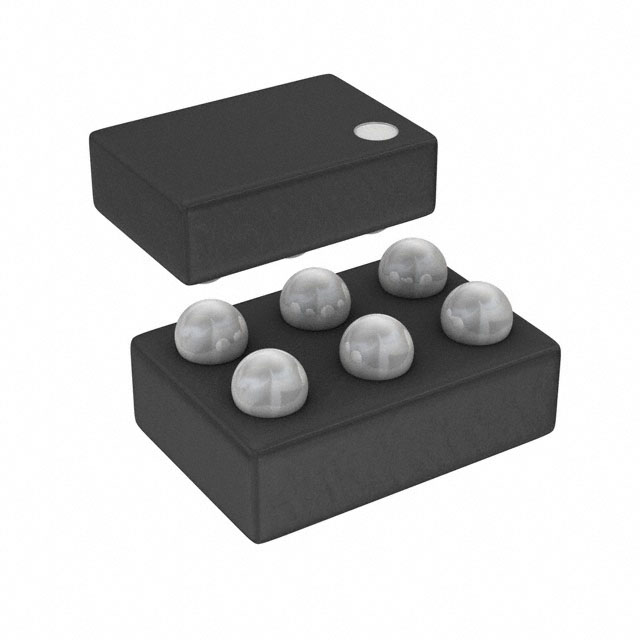
Low RDSON of 10 mΩ in 6-ball WLCSP
Wide input voltage range: 0 V to 5.5 V
3 A continuous operating current at 70°C
Bias supply voltage range: 1.83 V to 5.5 V
Low 26 µA ground (quiescent) current, VIN ≤ 3.4 V
Low 50 µA quiescent current, VIN = 5.5 V
Overtemperature protection circuitry
Low shutdown current: 1.2 V or VVB_EN = 1.83 V to 5.5 V,
VIN = 0.045 V to VVB_EN
0.0 V < VIN < 5.5 V, VVB_EN ≥ 1.83 V
See Figure 3
VIN = 0 V to 5.5 V, VVB_EN ≥ 1.83 V, CLOAD = 1 μF
See Figure 3
VIN = 0 V to 5.5 V, VVB_EN ≥ 1.83 V, CLOAD = 1 μF, ILOAD=10 mA
Shutdown Current
IOFF
Continuous Operating Current1
IOUT
VIN TO VOUT RESISTANCE
VOUT TURN-ON TIME
Turn-On Time
VOUT TURN-OFF TIME
Turn-Off Time
THERMAL SHUTDOWN
Thermal Shutdown Threshold
Thermal Shutdown Hysteresis
1
Symbol
VIN
VVB_EN
RDSON
tON
tOFF_TIME
TSSD
TSSD-HYS
Min
0
1.83
Typ
Max
5.5
5.5
Unit
V
V
1.83
V
V
V
V
MΩ
1.6
1.2
0.4
4
TJ rising
26
26
35
50
3.5
60
60
80
50
3
μA
μA
μA
μA
μA
μA
A
0.01
0.015
Ω
5.5
10
ms
150
800
μsec
125
15
°C
°C
At an ambient temperature of 85°C, the part can withstand a continuous current of ±2.22 A. At a load current of 3 A, the operational lifetime derates to 2190 hours.
TIMING DIAGRAM
VEN
TURN-ON
VOUT
11260-004
90%
TURN-OFF
10%
Figure 3. Timing Diagram
Rev. B | Page 3 of 12
�ADP1196
Data Sheet
ABSOLUTE MAXIMUM RATINGS
THERMAL RESISTANCE
Table 2.
Parameter
VIN to GND
VOUT to GND
VB_EN to GND
Continuous Drain Current
TA = 25°C
TA = 85°C
Continuous Diode Current
Storage Temperature Range
Operating Junction Temperature Range
Soldering Conditions
Rating
−0.3 V to +6.5 V
−0.3 V to VIN
−0.3 V to +6.5 V
Table 3. Typical θJA and ΨJB Values
±4 A
±2.22 A
−50 mA
−65°C to +150°C
−40°C to +105°C
JEDEC J-STD-020
ESD CAUTION
Package Type
6-Ball, 0.5 mm Pitch WLCSP
Stresses above those listed under Absolute Maximum Ratings
may cause permanent damage to the device. This is a stress
rating only; functional operation of the device at these or any
other conditions above those indicated in the operational
section of this specification is not implied. Exposure to absolute
maximum rating conditions for extended periods may affect
device reliability.
Rev. B | Page 4 of 12
θJA
260
ΨJB
58
Unit
°C/W
�Data Sheet
ADP1196
PIN CONFIGURATION AND FUNCTION DESCRIPTIONS
BALL A1
INDICATOR
1
2
VIN
VOUT
VIN
VOUT
A
B
VB_EN GND
TOP VIEW
(BALL SIDE DOWN)
Not to Scale
11260-003
C
Figure 4. Pin Configuration
Table 4. Pin Function Descriptions
Pin No.
A1, B1
A2, B2
C1
C2
Mnemonic
VIN
VOUT
VB_EN
GND
Description
Input Voltage.
Output Voltage.
Enable/Bias Input. Drive VB_EN high to turn on the switch, and drive VB_EN low to turn off the switch.
Ground.
Rev. B | Page 5 of 12
�ADP1196
Data Sheet
TYPICAL PERFORMANCE CHARACTERISTICS
VIN = 1.8 V, VVB_EN = 1.83 V, CIN = COUT = 1 µF, TA = 25°C, unless otherwise noted.
0.050
0.016
VIN = 0.2V
VIN = 1V
VIN = 3V
VIN = 5.5V
0.014
IOUT = 50mA
IOUT = 100mA
IOUT = 200mA
IOUT = 500mA
IOUT = 1000mA
IOUT = 3000mA
0.045
0.040
0.012
DIFFERENCE (V)
RDSON (Ω)
0.035
0.010
0.008
0.006
0.030
0.025
0.020
0.015
0.004
0.010
0.002
0
10
20
30
40
50
60
70
80
90
TEMPERATURE (°C)
0
11260-005
0
–40 –30 –20 –10
Figure 5. RDSON vs. Temperature, 50 mA, Different Input Voltages (VIN)
0
50
45
40
GROUND CURRENT (µA)
RDSON (Ω)
0.010
0.008
0.006
0.004
1.5
2.0
2.5
3.0
3.5
4.0
4.5
5.0
5.5
Figure 8. Voltage Drop vs. Input Voltage (VIN), Different Load Currents
VIN = 0.2V
VIN = 1V
VIN = 3V
VIN = 5.5V
0.012
1.0
INPUT VOLTAGE (V)
0.016
0.014
0.5
11260-008
0.005
IOUT = 100mA
IOUT = 200mA
IOUT = 500mA
IOUT = 1000mA
IOUT = 3000mA
35
30
25
20
15
10
0.002
10
20
30
40
50
60
70
80
90
TEMPERATURE (°C)
50
45
GROUND CURRENT (µA)
40
0.015
0.010
55
85
115
IOUT = 100mA
IOUT = 200mA
IOUT = 500mA
IOUT = 1000mA
IOUT = 3000mA
35
30
25
20
15
10
0.005
0
0
0.5
1.0
1.5
2.0
2.5
3.0
3.5
4.0
4.5
5.0
5.5
INPUT VOLTAGE (V)
Figure 7. RDSON vs. Input Voltage (VIN), Different Load Currents
0
–40
–5
25
55
TEMPERATURE (°C)
85
115
11260-010
5
11260-007
RDSON (Ω)
25
TEMPERATURE (°C)
IOUT = 50mA
IOUT = 100mA
IOUT = 200mA
IOUT = 500mA
IOUT = 1000mA
IOUT = 3000mA
0.020
–5
Figure 9. Ground Current vs. Temperature, Different Load Currents, VIN = 1.8 V
Figure 6. RDSON vs. Temperature, 3 A, Different Input Voltages (VIN)
0.025
0
–40
11260-006
0
11260-009
5
0
–40 –30 –20 –10
Figure 10. Ground Current vs. Temperature, Different Load Currents, VIN = 3.6 V
Rev. B | Page 6 of 12
�Data Sheet
90
GROUND CURRENT (µA)
80
20
IOUT = 100mA
IOUT = 200mA
IOUT = 500mA
IOUT = 1000mA
IOUT = 3000mA
SHUTDOWN CURRENT (µA)
100
ADP1196
70
60
50
40
30
VIN = 0.2V
VIN = 0.3V
VIN = 0.4V
VIN = 0.5V
VIN = 1.0V
VIN = 2.0V
VIN = 3.0V
VIN = 4.0V
VIN = 5.0V
VIN = 5.5V
16
12
8
4
20
25
–5
55
85
115
TEMPERATURE (°C)
0
–40
11260-011
0
–40
90
GROUND CURRENT (µA)
80
70
60
0
20
60
40
80
100
TEMPERATURE (°C)
Figure 11. Ground Current vs. Temperature, Different Load Currents, VIN = 5 V
100
–20
11260-014
10
Figure 14. Shutdown Current vs. Temperature, VOUT = 0 V,
Different Input Voltages (VIN)
T
VIN = 0.2V
VIN = 0.3V
VIN = 0.4V
VIN = 0.5V
VIN = 1.0V
VIN = 2.0V
VIN = 3.0V
VIN = 4.0V
VIN = 5.0V
VIN = 5.5V
ENABLE
2
INPUT CURRENT
1
50
VOUT
40
30
20
10
10000
1000
LOAD CURRENT (mA)
CH1 20mAΩ BW
CH3 500mV BW
Figure 12. Ground Current vs. Load Current,
Different Input Voltages (VIN)
8
VIN = 0.2V
VIN = 0.3V
VIN = 0.4V
VIN = 0.5V
VIN = 1.0V
BW
M1ms
T 10.6%
A CH2
1.18V
Figure 15. Typical Turn-On Time and Inrush Current,
VIN = 1.8 V, COUT = 47 μF, 330 Ω Load
VIN = 2.0V
VIN = 3.0V
VIN = 4.0V
VIN = 5.0V
VIN = 5.5V
T
2
ENABLE
6
INPUT CURRENT
1
VOUT
4
2
3
–20
0
20
40
60
80
TEMPERATURE (°C)
100
CH1 50mAΩ BW
CH3 500mV BW
Figure 13. Shutdown Current vs. Temperature,
Different Input Voltages (VIN), VOUT Open
CH2 1V
BW
M1ms
T 10.6%
A CH2
1.18V
Figure 16. Typical Turn-On Time and Inrush Current,
VIN = 1.8 V, COUT = 100 μF, 330 Ω Load
Rev. B | Page 7 of 12
11260-016
0
–40
11260-013
SHUTDOWN CURRENT (µA)
10
CH2 1V
11260-015
100
11260-012
3
0
10
�ADP1196
Data Sheet
T
T
2
2
ENABLE
ENABLE
INPUT CURRENT
INPUT CURRENT
1
1
VOUT
VOUT
3
BW
M1ms
T 10.6%
A CH2
1.18V
3
CH1 20mAΩ BW
CH3 2V BW
Figure 17. Typical Turn-On Time and Inrush Current,
VIN = 3.3 V, COUT = 47 μF, 330 Ω Load
CH2 1V
BW
M1ms
T 10.6%
A CH2
1.18V
11260-019
CH2 1V
11260-017
CH1 20mAΩ BW
CH3 1V BW
Figure 19. Typical Turn-On Time and Inrush Current,
VIN = 5 V, COUT = 47 μF, 330 Ω Load
T
T
2
2
ENABLE
ENABLE
INPUT CURRENT
INPUT CURRENT
1
1
VOUT
VOUT
CH2 1V
BW
M1ms
T 10.6%
A CH2
1.18V
11260-018
CH1 50mAΩ BW
CH3 1V BW
CH1 50mAΩ BW
CH3 2V BW
CH2 1V
BW
M1ms
T 10.6%
A CH2
1.18V
Figure 20. Typical Turn-On Time and Inrush Current,
VIN = 5 V, COUT = 100 μF, 330 Ω Load
Figure 18. Typical Turn-On Time and Inrush Current,
VIN = 3.3 V, COUT = 100 μF, 330 Ω Load
Rev. B | Page 8 of 12
11260-020
3
3
�Data Sheet
ADP1196
THEORY OF OPERATION
VIN
VOUT
VIN
VOUT
The ADP1196 supports 3 A of continuous current as long as TA is
less than or equal to 70°C. At 85°C, the derated load current falls to
±2.22 A.
The overtemperature protection circuit is activated if the load
current causes the junction temperature to exceed 125°C. When
this occurs, the overtemperature protection circuitry disables the
output until the junction temperature falls below approximately
110°C, at which point the output is reenabled. If the fault condition
persists, the output cycles off and on until the fault is removed.
GND
SUPPLY SWITCH
ENABLE LOGIC
CHARGE PUMP,
OVERCURRENT,
AND SLEW RATE
CONTROL
OVERTEMPERATURE
PROTECTION
11260-021
VB_EN
Figure 21. Functional Block Diagram
The ADP1196 is a high-side or low-side N-channel metal oxide
semiconductor (NMOS) load switch that is controlled by an
internal charge pump. The ADP1196 operates with voltages
from 1.83 V to 5.5 V on either VIN or VB_EN.
ESD protection structures are shown in the block diagram as
Zener diodes (see Figure 21).
The ADP1196 is a low quiescent current device with a nominal
4 MΩ pull-down resistor on its enable pin (VB_EN). The package
is a space-saving 1.0 mm × 1.5 mm, 6-ball WLCSP.
Internal circuitry monitors the VIN and VB_EN pins, connecting
the internal power supply to the higher of the two voltages. This
operation allows the NMOS load switch to operate on the low
side of a particular load.
An internal charge pump biases the NMOS switch to achieve a
relatively constant, ultralow on resistance of 10 mΩ across the
entire supply range. The use of the internal charge pump also
allows for controlled turn-on times. Turning the NMOS switch
on and off is controlled by the enable input, VB_EN, which can
interface directly with 1.83 V logic signals when VIN is greater
than 1.8 V.
Rev. B | Page 9 of 12
�ADP1196
Data Sheet
APPLICATIONS INFORMATION
CAPACITOR SELECTION
ENABLE FEATURE
Output Capacitor
The ADP1196 uses the VB_EN pin to enable and disable the
VOUT pin under normal operating conditions. As shown in
Figure 23, when a rising voltage (VVB_EN) on the VB_EN pin
crosses the active threshold, VOUT turns on. When a falling
voltage (VVB_EN) on the VB_EN pin crosses the inactive
threshold, VOUT turns off.
The ADP1196 is designed for operation with small, spacesaving ceramic capacitors; however, it functions with most
commonly used capacitors when the effective series resistance
(ESR) value is carefully considered. The ESR of the output
capacitor affects the response to load transients. Use a typical
1 µF capacitor with an ESR of 0.1 Ω or less for good transient
response. Using a larger value of output capacitance improves
the transient response to large changes in load current.
4.0
VOUT AT 3.6V
3.5
3.0
Input Bypass Capacitor
2.5
VOUT (V)
Connecting at least 1 µF of capacitance from VIN to GND reduces
the circuit sensitivity to the PCB layout, especially when high
source impedance or long input traces are encountered. When
greater than 1 µF of output capacitance is required, increase the
input capacitor to match it.
1.0
IOUT = 50mA
IOUT = 100mA
IOUT = 200mA
IOUT = 500mA
IOUT = 1000mA
IOUT = 3000mA
GROUND CURRENT (µA)
80
70
0
0
0.2
0.6
0.4
0.8
1.0
1.2
ENABLE VOLTAGE (V)
11260-023
0.5
The major source of ground current in the ADP1196 is the
internal charge pump for the field effect transistor (FET) drive
circuitry. Figure 22 shows the typical ground current when
VVB_EN = 1.83 V and VIN varies from 0.2 V to 5.5 V.
90
VVB_EN
RISING
1.5
GROUND CURRENT
100
VVB_EN
FALLING
2.0
Figure 23. Typical VB_EN Operation
As shown in Figure 23, the VB_EN pin has hysteresis built into
it. This built-in hysteresis prevents on/off oscillations that can
occur due to noise on the VB_EN pin as it passes through the
threshold points.
The VB_EN pin active/inactive thresholds derive from the VIN
voltage; therefore, these thresholds vary with changing input
voltages. Figure 24 shows the typical VB_EN active/inactive
threshold when the input voltage varies from 1.83 V to 5.5 V.
60
50
40
1.2
30
VVB_EN RISE
VVB_EN FALL
20
1.0
0.5
1.0
1.5
2.0
2.5
3.0
3.5
INPUT VOLTAGE (V)
4.0
4.5
5.0
5.5
Figure 22. Ground Current vs. Input Voltage, Different Load Currents
0.8
0.6
0.4
0.2
0
1.8
2.2
2.6
3.0
3.4
3.8
4.2
4.6
5.0
5.4
INPUT VOLTAGE (V)
Figure 24. Typical VB_EN Threshold vs. Input Voltage (VIN)
Rev. B | Page 10 of 12
11260-024
0
VB_EN THRESHOLD (V)
0
11260-122
10
�Data Sheet
ADP1196
TIMING
Turn-on delay is defined as the interval between the time that
VVB_EN exceeds the rising threshold voltage and when VOUT rises
to ~10% of its final value. The ADP1196 includes circuitry that has
a typical 2 ms turn-on delay and a controlled rise time to limit
the VIN inrush current. As shown in Figure 25 and Figure 26,
the turn-on delay is nearly independent of the input voltage.
The turn-off time is defined as the time it takes for the output
voltage to fall from 90% to 10% of VOUT. It is also dependent on
the RC time constant of the output capacitance and load resistance.
Figure 27 shows the typical turn-off times with VIN = 1.8 V, VIN =
3.3 V, and VIN = 5.0 V, COUT = 47 μF, and RLOAD = 330 Ω.
6.0
VVB_EN
VIN = 5.0V
VIN = 3.3V
VIN = 1.8V
5.0
T
VOUT (V)
4.0
2
ENABLE
3.0
INPUT CURRENT
2.0
1
VOUT
0
0
0.01
0.02 0.03
0.04 0.05
0.06
0.07
TIME (SEC)
3
CH2 1V
BW
M1ms
T 10.6%
A CH2
1.18V
Figure 27. Typical Turn-Off Time, VIN = 1.8 , VIN = 3.3 V, and VIN = 5.0 V,
COUT = 47 μF, RLOAD = 330 Ω
11260-025
CH1 20mAΩ BW
CH3 500mV BW
THERMAL OVERLOAD PROTECTION
Figure 25. Typical Turn-On Time and Inrush Current,
VIN = 1.8 V, COUT = 47 μF, 330 Ω Load
Thermal overload protection is included, which limits the junction
temperature to a maximum of 125°C (typical). Under extreme
conditions (that is, high ambient temperature and/or high power
dissipation), when the junction temperature starts to rise above
125°C, the output is turned off, reducing the output current to
zero. When the junction temperature falls below 110°C, the
output is turned on again, and output current is restored to its
operating value.
T
2
ENABLE
INPUT CURRENT
If the self-heating of the junction is great enough to cause its
temperature to rise above 125°C, thermal shutdown is activated,
turning off the output and reducing the output current to zero.
As the junction temperature cools and falls below 110°C, the
output turns on and conducts current into the load, again
causing the junction temperature to rise above 125°C. This
thermal oscillation between 110°C and 125°C causes a current
oscillation between the load current and 0 mA that continues as
long as the load remains connected to the output.
1
CH1 20mAΩ BW
CH3 2V BW
CH2 1V
BW
M1ms
T 10.6%
A CH2
1.18V
11260-026
VOUT
3
0.08 0.09 0.10
11260-027
1.0
Figure 26. Typical Turn-On Time and Inrush Current,
VIN = 5 V, COUT = 47 μF, 330 Ω Load
The rise time is defined as the time it takes the output voltage
(VOUT) to rise from 10% to 90% of its final value. The output
voltage rise time is dependent on the rise time of the internal
charge pump.
The thermal limit protection is intended to protect the device
against accidental overload conditions. For reliable operation,
device power dissipation must be externally limited so that the
junction temperature does not exceed 125°C.
For very large values of output capacitance, the RC time constant
(where C is the load capacitance (CLOAD) and R is the RDSON||RLOAD)
can become a factor in the rise time of the output voltage. Because
RDSON is much smaller than RLOAD, an adequate approximation
for RC is RDSON × CLOAD. An input or load capacitor is not required
for the ADP1196, although capacitors can be used to suppress
noise on the board.
Rev. B | Page 11 of 12
�ADP1196
Data Sheet
OUTLINE DIMENSIONS
1.000
0.950
0.900
2
1
A
BALL A1
IDENTIFIER
1.500
1.450
1.400
1.00
REF
C
0.50
BSC
TOP VIEW
(BALL SIDE DOWN)
0.675
0.595
0.515
B
0.50 BSC
BOTTOM VIEW
0.380
0.355
0.330
SIDE VIEW
(BALL SIDE UP)
0.345
0.295
0.245
SEATING
PLANE
0.270
0.240
0.210
11-08-2012-B
COPLANARITY
0.075
Figure 28. 6-Ball Wafer Level Chip Scale Package [WLCSP]
(CB-6-2)
Dimensions shown in millimeters
ORDERING GUIDE
Model1
ADP1196ACBZ-02-R7
1
Temperature Range
−40°C to +85°C
Package Description
6-Ball Wafer Level Chip Scale Package [WLCSP]
Z = RoHS Compliant Part.
©2013–2014 Analog Devices, Inc. All rights reserved. Trademarks and
registered trademarks are the property of their respective owners.
D11260-0-4/14(B)
Rev. B | Page 12 of 12
Package Option
CB-6-2
Branding
CK
�