HMC7545AxLP47
14.2 Gbps 4-Channel Asynchronous Signal Conditioner
Evaluation Board (EVB) User Guide
User Guide
Part # 140-00153-00
ECN# CP140238
Hittite Microwave Corporation
2 Elizabeth Dr Chelmsford, MA 01824
United States
www.hittite.com
140-00153-00
Revision A
March 11, 2014
Hittite Microwave Corporation Proprietary
Page 1 of 26
�HMC7545AxLP47 4-Channel Signal Conditioner
Evaluation Board User Guide
Contents
Introduction
p. 3
HMC7545AxLP47 EVB Signal Descriptions
p. 6
HMC7545AxLP47 Operational Modes
p. 7
HMC7545AxLP47 EVB Lab Equipment Configuration
p. 14
HMC7545AxLP47 EVB Operating Instructions
p. 15
HMC7545AxLP47 EVB Equalization (EQ) and De-Emphasis (DE) Operation
p. 23
140-00153-00
Revision A
March 11, 2014
Hittite Microwave Corporation Proprietary
Page 2 of 26
�HMC7545AxLP47 4-Channel Signal Conditioner
Evaluation Board User Guide
1
Introduction
The HMC7545AxLP47 is a uni-directional quad channel asynchronous signal conditioner designed for
serial links, operating up to 14.2 Gbps, of short and intermediate optical modules, linecards, and
backplane applications. HMC7545AxLP47 can be used either on the receiver or transmitter path for
compensating signal impairments by means of input Equalization (EQ) and output De-Emphasis (DE)
functions. The HMC7545AxLP47 is protocol and datarate agnostic and ideal for SAS/SATA, PCIe,
Fibre Channel, Infiniband, and Ethernet applications.
The HMC7545AxLP47 4-Channel Signal Conditioner Evaluation Board (EVB) is available for internal
characterization at Customer sites. This document provides operating instructions and guidelines for the
HMC7545AxLP47 EVB. There are two versions of this part: HMC7545ABLP47 2-Tap FIR Tx and
HMC7545AALP47 3-Tap FIR Tx. Please refer to the HMC7545AxLP47 datasheet for product
specifications.
The HMC7545AxLP47 operates at data rates up to 14.2 Gb/s. Its primary function is to compensate for
channel losses due to long backplane, or other lengthy system PCB traces using FR4 dielectric
transmission lines, for example. These compensation circuits consist of channel equalization (EQ) at the
inputs, and channel pre-emphasis (PE) at the outputs, as shown in the functional diagram in Figure 1.
The HMC7545AxLP47 typically operates on a +2.5V power supply, but can also run on +3.3V. The
HMC7545AxLP47 operation is specified at 88 mW/ channel under typical conditions.
All 4 input and 4 output signals of the HMC7545AxLP47 4-Channel Signal Conditioner are accessible
via SMA connectors on the EVB. This is shown in Figure 2. The input channels are: IN0P/N, IN1P/N
IN2P/N, IN3P/N and the output channels are: OUT0P/N OUT1P/N, OUT2P/N, OUT3P/N. These I/O
channel signals are AC-coupled on the EVB using 100nF ultra-broadband coupling capacitors to
facilitate interfacing to ground-referenced test equipment, such as PRBS pattern generators (inputs), and
Oscilloscopes (outputs).
Transmission line load boards of various lengths, and representing real-world lossy channel conditions,
can be attached to the EVB via the SMA connectors at inputs or outputs. Lossy channels can be used in
this way to demonstrate the Signal Integrity improvements of the Pre-Emphasis (PE) and Equalization
(EQ) features of the HMC7545AxLP47.
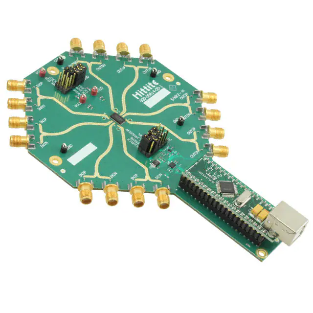
A photograph of the physical HMC7545AxLP47 EVB is given in Figure 3, and shows component
locations, power connections, USB connector, jumpers, and I/O signal orientation.
The HMC7545AxLP47 can be configured via one of the three modes of operation, as described, below.
1) Parallel Mode
Parallel Mode uses jumpers provided on the EVB to configure the HMC7545AxLP47.
2) I2C Mode
The HMC7545AxLP47 EVB Graphical User Interface (GUI) is used in I2C mode to set the values of
the internal registers to default settings, or user-defined values. A register map is included in the data
sheet.
140-00153-00
Revision A
March 11, 2014
Hittite Microwave Corporation Proprietary
Page 3 of 26
�HMC7545AxLP47 4-Channel Signal Conditioner
Evaluation Board User Guide
3) EEPROM Mode
This mode uses the EEPROM on the EVB to store register values. The GUI is used to enter and
optimize these settings. The HMC7545AxLP47 will then operate using the settings stored on the
EEPROM.
140-00153-00
Revision A
March 11, 2014
Rx_EQ0
Rx_EQ1
MODE
Tx_EQ0
Tx_EQ1
TXDOUT
Figure 1: HMC7545AxLP47 4-Channel Signal Conditioner: Functional Diagram
36
35
34
33
32
31
IN0P
1
30
OUT0P
IN0N
2
29
OUT0N
VCCO
VCCI
3
28
IN1P
4
27
OUT1P
IN1N
5
26
OUT1N
25
VCCO
VCCI
6
VCCI
7
IN2P
4 Channel Signal
Conditioner
(4x7 mm QFN
package)
22
OUT2N
10
21
VCCO
IN3P
11
20
OUT3P
IN3N
12
19
OUT3N
13
14
15
16
17
18
SDA
9
VCCI
SCK
IN2N
I2C SEL
OUT2P
I2C_MAS/SLW
23
RESETB
VCCO
8
SQUELCH
24
Hittite Microwave Corporation Proprietary
Page 4 of 26
�HMC7545AxLP47 4-Channel Signal Conditioner
Evaluation Board User Guide
Figure 2: HMC7545AxLP47 4-Channel Signal Conditioner: Pin Names
Figure 3. Photo of HMC7545AxLP47 Evaluation Board (EVB)
140-00153-00
Revision A
March 11, 2014
Hittite Microwave Corporation Proprietary
Page 5 of 26
�HMC7545AxLP47 4-Channel Signal Conditioner
Evaluation Board User Guide
2
HMC7545AxLP47 Signal Descriptions
Table 1 summarizes the HMC7545AxLP47 signals and their respective functions.
Table 1: HMC7545AxLP47 Signal Names and Functions
Signal Name
Signal Description
IN(0-3)P and N
OUT(0-3P) and N
VCCI
VCCO
Differential RF inputs with independent programmable Equalization (EQ)
Differential RF outputs with independent programmable De-Emphasis (DE)
Power supply pin for all inputs
Power supply pin for all outputs
SQUELCH
RESETB
SQUELCH all outputs. Active HI = 1
Global RESET. Active LO = 0
I2C Master Mode, or Slave Mode Select.
Master = HI = 1, Slave = LO = 0
Parallel Mode, or I2C Mode Select
Parallel Mode = LO = 0, I2C Mode = HI = 1
Clock pin for the 2 wire interface (I2C/TWI)
Data pin for the 2 wire interface (I2C/TWI)
I2C_MAS/SLV
I2CSEL
SCK
SDA
RX_EQ0
RX_EQ1
MODE
TX_EQ0
TX_EQ1
TXDOUT
140-00153-00
Revision A
March 11, 2014
LSB of the CTLE settings while in parallel mode
MSB of the CTLE settings while in parallel mode
Selects between high and low speed operation
Dual purpose:
- Set the chip address in I2C Mode.
- LSB of De-Emphasis settings in Parallel Mode
Dual purpose:
- Set the chip address in I2C Mode.
- MSB of De-Emphasis settings in Parallel Mode
Dual purpose:
- Set the chip address in I2C Mode.
- Set the amplitude in parallel mode
Hittite Microwave Corporation Proprietary
Page 6 of 26
�HMC7545AxLP47 4-Channel Signal Conditioner
Evaluation Board User Guide
3
HMC7454AxLP47E EVB Operational Modes
The HMC7454AxLP47E provides three modes of operation: 1) Parallel mode using jumpers on EVB, 2)
I2C mode using GUI PC interface, and 3) EEPROM mode, from EEPROM on EVB.
3.1
Parallel Mode (Direct Pin Control)
There are two banks of jumpers on the HMC7545AxLP47 EVB. Each bank has six signals that can be
set to 1 = VCC, 0 = GND, or X = MID-LEVEL via. jumpers. The jumpers are shown in the EVB photo
provided in Figure 3. The signals and nominal jumper settings are provided in Tables 2 and 3, below.
Table 2: Parallel Mode: Jumper Bank 1
Signal Name
SQUELCH
RESETB
I2C_MAS/SLV
I2CSEL
SCK
SDA
Signal Description
SQUELCH all outputs. Active HI
Global RESET. Active LO
I2C Master Mode, or Slave Mode Select.
Master = HI, Slave = LO
Parallel Mode (LO) or normal I2C Mode
(HI) Select
Clock pin for the 2 wire interface
Data pin for the 2 wire interface
Parallel Mode Settings
0 = GND
1 = VCC
0 = GND
0 = GND
X = MID-LEVEL
X = MID-LEVEL
Table 3: Parallel Mode: Jumper Bank 2
Signal Name
RX_EQ0
RX_EQ1
MODE
TX_EQ0
TX_EQ1
TXDOUT
140-00153-00
Revision A
March 11, 2014
Signal Description
LSB of the CTLE settings while in parallel
mode
MSB of the CTLE settings while in parallel
mode
Selects high or low speed operation:
Low Speed = LO, High Speed = HI
Dual purpose:
- Set the chip address in I2C Mode.
- LSB of De-Emphasis settings in
Parallel Mode
Dual purpose:
- Set the chip address in I2C Mode.
- MSB of De-Emphasis settings in
Parallel Mode
Dual purpose:
- Set the chip address in I2C Mode.
- Set the amplitude in parallel mode
Parallel Mode Settings
Per Table 4
Default: X = MID-LEVEL
Per Table 4
Default: X = MID-LEVEL
1 = VCC
Per Table 5
Default: 0 = GND
Per Table 5
Default: 0 = GND
Per Table 5
Default: 0 = GND
Hittite Microwave Corporation Proprietary
Page 7 of 26
�HMC7545AxLP47 4-Channel Signal Conditioner
Evaluation Board User Guide
Pins RX_EQ[1:0] control the Rx CTLE EQ settings. These pins are tri-state control pins. The three
different levels are defined as follows, as shown in Table 4.
0 = GND
X = MID-LEVEL
1 = VCC
Table 4: Input Rx EQ: Parallel Mode (Direct Pin Control) Range of Settings
140-00153-00
Revision A
March 11, 2014
EQ_LEVEL[1:0]
(decimal)
00 (1)
CTLE Equalization
(dB)
-1.1
0X (2)
-2.8
01 (3)
-4.6
X0 (4)
-5.4
XX (5)
-7.3
X1 (6)
-9.1
10 (7)
-12.2
1X (8)
-15.5
11 (9)
-17.8
Hittite Microwave Corporation Proprietary
Page 8 of 26
�HMC7545AxLP47 4-Channel Signal Conditioner
Evaluation Board User Guide
Pins TXDOUT and TX_EQ[1:0] control the TX DE settings. These pins are tri-state control pins. The
three different levels are defined as follows, as shown in Table 5.
0 = GND
X = MID-LEVEL
1 = VCC
Table 5: Output Tx DE: Parallel Mode (Direct Pin Control) Range of Settings
140-00153-00
Revision A
March 11, 2014
TXDOUT
TX_EQ[1:0]
De-Emphasis (dB)
0
0
0
0
0
0
0
0
0
1
1
1
1
1
1
1
1
1
2
2
2
2
2
2
2
2
2
00
0X
X0
01
XX
X1
10
1X
11
00
0X
01
X0
XX
X1
10
1X
11
00
0X
01
X0
XX
X1
10
1X
11
0
-1.63
-3.3
-5.02
-6.85
-8.83
-11.06
-13.66
-16.9
0
-1.63
-3.3
-5.02
-6.85
-8.83
-11.06
-13.66
-16.9
0
-1.11
-2.23
-3.6
-5.38
-7.71
-11.87
-15.72
-19.4
Note
Hittite Microwave Corporation Proprietary
PCI 1
PCI 2
PCI 5
PCI 3
PCI 6
8db
10db
12db
12db
PCI 1
PCI 2
PCI 3
PCI 5
PCI 6
8db
10db
12db
12db
PCI 1
PCI 2
PCI 3
PCI 5
PCI 6
8db
10db
12db
12db
Page 9 of 26
�HMC7545AxLP47 4-Channel Signal Conditioner
Evaluation Board User Guide
3.2
I2C Mode (GUI control)
I2C mode is the standard method to operate, and evaluate the HMC7545AxLP47 using the EVB. This
mode uses I2C communications and the Graphical User Interface (GUI) via PC to set register values for
optimized signal conditioner performance.
There are two banks of jumpers on the HMC7545AxLP47 EVB. Each bank has six signals that can be
set to 1 = VCC, 0 = GND, or X = MID-LEVEL via. jumpers. The jumpers are shown in the EVB photo
provided in Figure 3. The signals and nominal jumper settings are provided in Tables 6 and 7, below.
Table 6: I2C Mode: Jumper Bank 1
Signal Name
SQUELCH
RESETB
I2C_MAS/SLV
I2CSEL
SCK
SDA
Signal Description
SQUELCH all outputs. Active HI
Global RESET. Active LO
I2C Master Mode, or Slave Mode Select.
Master = HI, Slave = LO
Parallel Mode (LO) or normal I2C Mode
(HI) Select
Clock pin for the 2 wire interface
Data pin for the 2 wire interface
I2C Mode Settings
0 = GND
1 = VCC
0 = GND
1 = VCC
X = MID-LEVEL
X = MID-LEVEL
Table 7: I2C Mode: Jumper Bank 2
Signal Name
RX_EQ0
RX_EQ1
MODE
TX_EQ0
TX_EQ1
TXDOUT
140-00153-00
Revision A
March 11, 2014
Signal Description
LSB of the CTLE settings while in parallel
mode
MSB of the CTLE settings while in parallel
mode
Selects high or low speed operation:
Low Speed = LO, High Speed = HI
Dual purpose:
- Set the chip address in I2C Mode.
- LSB of De-Emphasis settings in
Parallel Mode
Dual purpose:
- Set the chip address in I2C Mode.
- MSB of De-Emphasis settings in
Parallel Mode
Dual purpose:
- Set the chip address in I2C Mode.
- Set the amplitude in parallel mode
I2C Mode Settings
X = MID-LEVEL
X = MID-LEVEL
1 = VCC
X = MID-LEVEL
0 = GND
0 = GND
Hittite Microwave Corporation Proprietary
Page 10 of 26
�HMC7545AxLP47 4-Channel Signal Conditioner
Evaluation Board User Guide
In I2C mode, the input EQ settings are controlled by the REG10[4:0] bits (EQ_LEVEL[4:0]). The
amount of equalization achieved for each value in this register for CTLE EQ is shown in Table 8.
Table 8: Input Rx EQ:I2C Mode Settings
EQ_LEVEL[4:0]
(dec)
0
1
2
3
4
5
6
7
8
9
10
11
12
13
14
15
dB
0
-0.3
-0.7
-1.1
-1.5
-1.8
-2.2
-2.5
-2.8
-3.1
-3.4
-3.7
-4
-4.3
-4.6
-4.8
EQ_LEVEL[4:0]
(dec)
16
17
18
19
20
21
22
23
24
25
26
27
28
29
30
31
dB
-5.1
-5.4
-5.7
-6.1
-6.4
-6.9
-7.3
-7.8
-8.4
-9.1
-10
-11
-12.2
-13.7
-15.5
-17.8
Output DE setting range for I2C Mode is given in Table 9.
Table 9: Output Tx DE: I2C Mode Settings
3.3
Register/bits
Function
REG5[3:0]
TX_PRE[3:0]
REG6[4:0]
TX_MAIN[4:0]
REG7[5:0]
TX_POST[5:0]
REG8[4:0]
DELAY1[4:0]
REG9[4:0]
DELAY2[4:0]
EEPROM Mode
The HMC7545AxLP47 EVB Graphical User Interface (GUI) is also used to update/optimize register
values for EQ and DE in EEPROM mode. The EEPROM will operate as I2C Slave and the
HMC7545AxLP47 will operate as I2C Master in EEPROM Mode. EEPROM programming can be done
with or without the HMC7545 DUT present on the board.
140-00153-00
Revision A
March 11, 2014
Hittite Microwave Corporation Proprietary
Page 11 of 26
�HMC7545AxLP47 4-Channel Signal Conditioner
Evaluation Board User Guide
The eval board contains a PCA24S08A, 1024 × 8-bit CMOS EEPROM, with access protection. The
EEPROM memory addressing is shown in Figure 4. The target settings for the HMC7545 in master
mode must be programmed in the right sequence starting at byte 0. RESETB must be toggled after VCC
is stable from LO to HI in order to load EEPROM.
Both the DUT and the EEPROM are connected to the I2C bus. The user must be careful to avoid
contention on the bus when the signal conditioner is present. This is usually resolved by the correct
addressing (chip address selection) for each part.
There are two banks of jumpers on the HMC7545AxLP47 EVB. Each bank has six signals that can be
set to 1 = VCC, 0 = GND, or X = MID-LEVEL via. jumpers. The jumpers are shown in the EVB photo
provided in Figure 3. The signals and nominal jumper settings are provided in Tables 10 and 11, below.
Table 10: EEPROM Mode: Jumper Bank 1
Signal Name
SQUELCH
RESETB
I2C_MAS/SLV
I2CSEL
SCK
SDA
Signal Description
SQUELCH all outputs. Active HI
Global RESET. Active LO
I2C Master Mode, or Slave Mode Select.
Master = HI, Slave = LO
Parallel Mode (LO) or normal I2C Mode
(HI) Select
Clock pin for the 2 wire interface
Data pin for the 2 wire interface
EEPROM Mode Settings
0 = GND
1 = VCC
1 = VCC
1 = VCC
X = MID-LEVEL
X = MID-LEVEL
Table 11: EEPROM Mode: Jumper Bank 2
Signal Name
RX_EQ0
RX_EQ1
MODE
TX_EQ0
TX_EQ1
TXDOUT
140-00153-00
Revision A
March 11, 2014
Signal Description
LSB of the CTLE settings while in parallel
mode
MSB of the CTLE settings while in parallel
mode
Selects high or low speed operation:
Low Speed = LO, High Speed = HI
Dual purpose:
- Set the chip address in I2C Mode.
- LSB of De-Emphasis settings in
Parallel Mode
Dual purpose:
- Set the chip address in I2C Mode.
- MSB of De-Emphasis settings in
Parallel Mode
Dual purpose:
- Set the chip address in I2C Mode.
- Set the amplitude in parallel mode
EEPROM Mode Settings
X = MID-LEVEL
X = MID-LEVEL
1 = VCC
X = MID-LEVEL
0 = GND
0 = GND
Hittite Microwave Corporation Proprietary
Page 12 of 26
�HMC7545AxLP47 4-Channel Signal Conditioner
Evaluation Board User Guide
Figure 4. EEPROM Memory Addressing Diagram
140-00153-00
Revision A
March 11, 2014
Hittite Microwave Corporation Proprietary
Page 13 of 26
�HMC7545AxLP47 4-Channel Signal Conditioner
Evaluation Board User Guide
4
HMC7545AxLP47 EVB Test Equipment Configuration
The test equipment requirements, and setup configuration are shown below in Figures 5 and 6.
Figure 5. HMC7545AxLP47 EVB Test Equipment Setup: Block Diagram
Figure 6. HMC7545AxLP47 EVB Test Equipment Setup: Physical Diagram
140-00153-00
Revision A
March 11, 2014
Hittite Microwave Corporation Proprietary
Page 14 of 26
�HMC7545AxLP47 4-Channel Signal Conditioner
Evaluation Board User Guide
5
HMC7545AxLP47 EVB Operating Instructions
5.1
Parallel Mode. HMC7545AxLP47 EVB Operating Instructions
1) Configure the DUT using jumpers per Tables 2 and 3, as described in section 3.1, Parallel Mode
Operaton.
2) Connect +2.5V/GND(0V) power supply to the EVB using the clips on the connection points as
shown in EVB Figure 3.
3) Connect the USB cable from the PC to the USB port on the USB-to-I2C interface module
located on the EVB, as shown in Figure 3. This step is optional in Parallel Mode.
4) Turn on +2.5V/0V power supply. VCC supply current and Vout are approximately 90-130mA,
and 330mVppd, respectively, using default conditions in Parallel Mode.
5) Adjust EQ + DE settings by changing the jumper settings to obtain optimized data eye at output.
Use Tables 4 and 5 as a guide.
5.2
I2C Mode Operation
5.2.1
HMC7545AxLP47 EVB Graphical User Interface (GUI) Installation Instructions
Use the Installation CD supplied with the Installation Kit to install the GUI on your PC. MS Win.XP, or
7 OS is recommended.
Insert the CD into your PC CD Drive. This will run the setup.exe installer. Progress through the popup
menus and prompts, and click Finish when complete.
Figure 7: GUI Installer Pop Up Menu #1
140-00153-00
Revision A
March 11, 2014
Hittite Microwave Corporation Proprietary
Page 15 of 26
�HMC7545AxLP47 4-Channel Signal Conditioner
Evaluation Board User Guide
Figure 8: GUI Installer Pop Up Menu #2
Figure 9: GUI Installer Pop Up Menu #3
Figure 10: GUI Installer Pop Up Menu #4
140-00153-00
Revision A
March 11, 2014
Hittite Microwave Corporation Proprietary
Page 16 of 26
�HMC7545AxLP47 4-Channel Signal Conditioner
Evaluation Board User Guide
5.2.2
HMC7545AxLP47 EVB GUI Operating Instructions
After installation of the GUI on your PC is complete, the GUI will be ready to operate after connecting
the USB interface cable and +2.5V power supply to the EVB.
1) Configure the DUT using jumpers per Tables 6 and 7, as described in section 3.2, I2C Mode
Operaton.
2) Connect +2.5V/GND(0V) power supply to the EVB using the clips on the connection points as
shown in EVB Figure 3.
3) Connect the USB cable from the PC to the USB port on the USB-to-I2C interface module
located on the EVB, as shown in Figure 3.
4) Turn on +2.5V/0V power supply. Power supply current range is 90mA to 130mA under typical
operating conditions.
5) Run GUI software program to configure the HMC7545AxLP47 4-Channel Signal Conditioner
for operation. The GUI will automatically connect to the EVB via the I2C-to-USB interface.
Once connected, the display in the upper right of the GUI will change to from red to green, and
the text will change to Connected.
The electrical configuration for the HMC7545AxLP47 EVB is controlled via the Graphical User
Interface (GUI). The GUI consists of a single tab / page. There are two separate GUI pages, one for
HMC7545ABLP47 2-Tap FIR Tx and one for HMC7545AALP47 3-Tap FIR Tx. The different pages
are auto selected by the chip address which is different between the two design versions.
Any, or all of the HMC7545AxLP47 channels 0-3 may be used for evaluation.
Please see HMC7545AxLP47 Register Map for detailed register information.
6) Verify that the +2.5V Power Supply Current is within the ranges as per Table 12, below.
7) GUI Settings: The default Registers/Functions settings are initially loaded into the
HMC7545AxLP47 as a starting point for Input EQ and Output DE optimizations. These values
are optimized for the back-to-back configuration, which consists of the 1) EVB, 2) SMA cables,
and 3) Test Equipment, but no load boards (loss channel). Tables 8 and 9, above, are provided
for reference. Please refer to Table 12, and Figure 11, below for the GUI default settings.
Table 12: I2C Mode Register and Parameter Initial Values
Register/Parameter Name
EQLEVEL
TXMAIN
TXPOST
I(VCC), (mA)
Vout, (mVppd)
140-00153-00
Revision A
March 11, 2014
Register/Parameter Value
I2C Mode Default
14 (d)
9 (d)
4 (d)
140
400
Hittite Microwave Corporation Proprietary
Page 17 of 26
�HMC7545AxLP47 4-Channel Signal Conditioner
Evaluation Board User Guide
Figure 11a. HMC7545ABLP47 2-Tap FIR Tx EVB GUI Settings for Back-to-Back
Configuration
140-00153-00
Revision A
March 11, 2014
Hittite Microwave Corporation Proprietary
Page 18 of 26
�HMC7545AxLP47 4-Channel Signal Conditioner
Evaluation Board User Guide
Figure 11b. HMC7545AALP47 3-Tap FIR Tx EVB GUI Settings for Back-to-Back
Configuration
5.3
EEPROM Mode. HMC7545AxLP47 EVB Operating Instructions
1) Configure the DUT as described in section 2.3, EEPROM Mode Operation.
2) Connect +2.5V/GND(0V) power supply to the EVB using the clips on the connection points as
shown in EVB Figure 3.
3) Connect the USB cable from the PC to the USB port on the USB-to-I2C interface module
located on the EVB, as shown in Figure 3.
4) Turn on +2.5V/0V power supply. Power supply current range is 80mA to 130mA under typical
operating conditions.
140-00153-00
Revision A
March 11, 2014
Hittite Microwave Corporation Proprietary
Page 19 of 26
�HMC7545AxLP47 4-Channel Signal Conditioner
Evaluation Board User Guide
5) Using the GUI, adjust EQ + DE settings to obtain optimized data eye at output.
6) After GUI optimization is complete, Click on “Write to EEPROM” button to update EEPROM
memory and save settings.
7) Remove USB cable from EVB
8) Toggle RESETB after VCC is stable from LO to HI in order to load EEPROM register values to
HMC7545AxLP47.
5.4
Basic Test Equipment Configuration and Setup: All Modes
1) Refer to Figures 5 and 6 in Section 4, above, for recommended test equipment setup
configuration.
2) Connect user input signal source (e.g.: PPG) to user-selected input channel(s) via SMA
connectors and cables. A transmission line load board that emulates a lossy channel may be
inserted between the source and the EVB.
3) Connect user measurement equipment (e.g.: oscilloscope) to user-selected output channel(s). A
transmission line load that emulates a lossy channel board may be inserted between the EVB and
the measurement equipment.
4) Turn on the pattern generator signal source.
5) Observe output(s) and update/optimize register settings via 1) I2C/GUI Mode, 2) Parallel Mode,
or 3) EEPROM Mode settings for Equalization (EQ), and/or De-Emphasis (DE) optimization, as
required.
Example HMC7545ABLP47 EVB data eye plots with default GUI settings, Vout ≈ 400mVppd, and
back-to-back configuration (EVB only), are provided, below in Figures 12a, 13a, and 14a.
Figure 12a. 14.0 Gbps (16G FC) Data Eye: Default Settings, Back-to-Back Configuration
140-00153-00
Revision A
March 11, 2014
Hittite Microwave Corporation Proprietary
Page 20 of 26
�HMC7545AxLP47 4-Channel Signal Conditioner
Evaluation Board User Guide
Figure 13a. 12.0 Gbps Data Eye: Default Settings, Back-to-Back Configuration
Figure 14a. 10.0 Gbps Data Eye: Default Settings, Back-to-Back Configuration
140-00153-00
Revision A
March 11, 2014
Hittite Microwave Corporation Proprietary
Page 21 of 26
�HMC7545AxLP47 4-Channel Signal Conditioner
Evaluation Board User Guide
Example HMC7545AALP47 EVB data eye plots with modified GUI settings, Vout ≈ 400mVppd, and
back-to-back configuration (EVB only), are provided, below in Figures 12b, 13b, and 14b.
Figure 12b. 14.0 Gbps (16G FC) Data Eye: Default Settings, Back-to-Back Configuration
Figure 13b. 12.0 Gbps Data Eye: Default Settings, Back-to-Back Configuration
140-00153-00
Revision A
March 11, 2014
Hittite Microwave Corporation Proprietary
Page 22 of 26
�HMC7545AxLP47 4-Channel Signal Conditioner
Evaluation Board User Guide
Figure 14b. 10.0 Gbps Data Eye: Default Settings, Back-to-Back Configuration
6
HMC7545AxLP47 EVB Equalization (EQ) and DeEmphasis (DE) Operation
The HMC7545ABLP47 2-Tap FIR Tx is used as the example for this section. The input Rx CTLE EQ
range is 18 dB and resolution is 0.75dB, and the output Tx DE range is 12dB and resolution is 0.75dB.
The reference points, as described, below, are given in the block diagram in Figure 15. Note that in
addition to the external load board loss, there is approximately -1dB loss for each of four input and four
output differential channels on the EVB. This is due to the on-PCB transmission lines, as shown in
Figure 3.
Example EQ and DE results are shown in Figures 16 & 17 and Figures 18 & 19, below.
Figure 16 shows a 12.0 Gb/s signal through a 10” load board (lossy channel emulator) only. Figure 17
shows the output after Equalization (EQ) for a 12.0 Gb/s input signal routed through the EVB with a 10”
load board lossy channel at the input.
Figure 18 shows a 12.0 Gb/s input signal through a 10” load board (lossy channel emulator) only.
Figure 19 shows the HMC7545AxLP47 output after De-Emphasis (DE) for a 12.0 Gb/s input signal
routed through the with a 10” load board lossy channel at the output.
140-00153-00
Revision A
March 11, 2014
Hittite Microwave Corporation Proprietary
Page 23 of 26
�HMC7545AxLP47 4-Channel Signal Conditioner
Evaluation Board User Guide
Figure 15. HMC7545AxLP47 Lossy Channel Block Diagram
140-00153-00
Revision A
March 11, 2014
Hittite Microwave Corporation Proprietary
Page 24 of 26
�HMC7545AxLP47 4-Channel Signal Conditioner
Evaluation Board User Guide
Figure 16. 12.0 Gb/s PRBS 29-1. 10”Load Board Lossy Channel Only, as Indicated
by Point 2 in Figure 15.
Figure 17. 12.0 Gb/s PRBS 29-1. HMC7545ABLP47 EVB with 10” Load Board
Lossy Channel at Input Using Equalization (EQ), as Indicated by Point 3 in Figure
15.
140-00153-00
Revision A
March 11, 2014
Hittite Microwave Corporation Proprietary
Page 25 of 26
�HMC7545AxLP47 4-Channel Signal Conditioner
Evaluation Board User Guide
Figure 18. 12.0 Gb/s PRBS 29-1. 10”Load Board Lossy Channel Only, as Indicated
by Point 4, with Source at Point 3 in Figure 15.
Figure 19. 12.0 Gb/s PRBS 29-1. HMC7545ABLP47 EVB with 10” Load Board
Lossy Channel at Output Using 4-Channel Signal Conditioner De-Emphasis (DE),
as Indicated by Point 4 in Figure 15.
140-00153-00
Revision A
March 11, 2014
Hittite Microwave Corporation Proprietary
Page 26 of 26
�


 工商网监
湘ICP备2023018690号
工商网监
湘ICP备2023018690号
