LTC4305
2-Channel,
2-Wire Bus Multiplexer with
Capacitance Buffering
U
FEATURES
■
■
■
■
■
■
■
■
■
■
DESCRIPTIO
1:2 2-Wire Multiplexer/Switch
Connect SDA and SCL Lines with 2-Wire Bus
Commands
Supply Independent Bidirectional Buffer for SDA
and SCL Lines Increases Fan-Out
Programmable Disconnect from Stuck Bus
Compatible with I2C and SMBus Standards
Rise Time Accelerator Circuitry
SMBus Compatible ALERT Response Protocol
Prevents SDA and SCL Corruption During Live Board
Insertion and Removal from Backplane
±10kV Human Body Model ESD Ruggedness
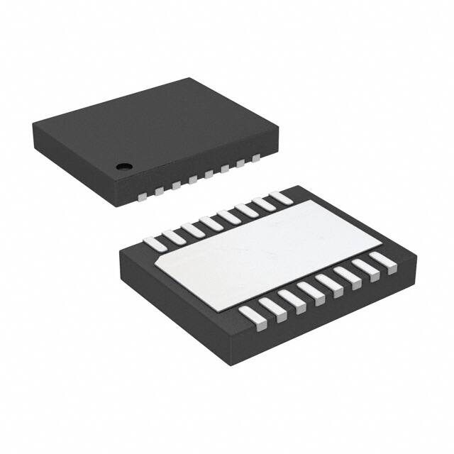
16-Lead (4mm × 5mm) DFN and SSOP Packages
U
APPLICATIO S
■
■
■
The LTC®4305 is a 2-channel, 2-wire bus multiplexer with
bus buffers to provide capacitive isolation between the
upstream bus and downstream buses. Through software
control, the LTC4305 connects the upstream 2-wire bus
to any desired combination of downstream channels.
Each channel can be pulled up to a supply voltage ranging
from 2.2V to 5.5V, independent of the LTC4305 supply
voltage. The downstream channels are also provided with
an ALERT1–ALERT2 inputs for fault reporting.
Programmable timeout circuitry disconnects the downstream buses if the bus is stuck low. When activated, rise
time accelerators source currents into the 2-wire bus pins
to reduce rise time. Driving the ENABLE pin low restores
all features to their default states. Three address pins
provide 27 distinct addresses.
The LTC4305 is available in 16-lead (4mm × 5mm) DFN
and SSOP packages.
Nested Addressing
5V/3.3V Level Translator
Capacitance Buffer/Bus Extender
, LTC and LT are registered trademarks of Linear Technology Corporation. All other
trademarks are the property of their respective owners. Patent Pending.
U
TYPICAL APPLICATIO
A Level-Shifting and Nested Addressing Application
I2C Bus Waveforms
3.3V
2.5V
VCC = 3.3V
0.01µF
10k
10k
10k
10k
10k
10k
VCC
MICROCONTROLLER
SCLIN
SCL1
SDAIN
SDA1
ALERT
ALERT1
SFP
MODULE #1
VBACK = 2.5V
SCLIN
2V/DIV
VCARD1 = 3.3V
SCL1
2V/DIV
ADDRESS = 1111 000
5V
LTC4305
10k
ADR2
ADR1
SCL2
ADR0
SDA2
GND
10k
10k
SFP
MODULE #2
VCARD2 = 5V
SCL2
2V/DIV
500ns/DIV
4305 TA01b
ALERT2
4305 TA01
ADDRESS = 1000 100
ADDRESS = 1111 000
4305f
1
�LTC4305
W W
U
W
ABSOLUTE
AXI U RATI GS (Note 1)
Supply Voltage (VCC) ................................... –0.3V to 7V
Input Voltages (ADR0, ADR1, ADR2,
ENABLE, ALERT1, ALERT2) .................... –0.3V to 7V
Output Voltages (ALERT, READY) ............... –0.3V to 7V
Input/Output Voltages (SDAIN, SCLIN,
SCL1, SDA1, SCL2, SDA2) ...................... –0.3V to 7V
Output Sink Current (SDAIN, SCLIN, SCL1,
SDA1, SCL2, SDA2, ALERT, READY) ............... 10mA
Operating Temperature Range
LTC4305C ............................................... 0°C to 70°C
LTC4305I ............................................. –40°C to 85°C
Storage Temperature Range
DHD Package .................................... –65°C to 125°C
GN Package ....................................... –65°C to 150°C
Lead Temperature (Soldering, 10 sec)
GN Package ...................................................... 300°C
U
U
W
PACKAGE/ORDER I FOR ATIO
TOP VIEW
TOP VIEW
ALERT2
1
16 SCL2
ALERT
2
15 SDA2
SDAIN
GND
4
SCLIN
5
ENABLE
VCC
ADRO
14 ALERT1
3
17
6
7
8
13 SDA1
12 SCL1
11 READY
10 ADR2
9
ADR1
DHD PACKAGE
16-LEAD (4mm × 5mm) PLASTIC DFN
ALERT2
1
16 SCL2
ALERT
2
15 SDA2
SDAIN
3
14 ALERT1
GND
4
13 SDA1
SCLIN
5
12 SCL1
ENABLE
6
11 READY
VCC
7
10 ADR2
ADR0
8
9
ADR1
GN PACKAGE
16-LEAD NARROW PLASTIC SSOP
TJMAX = 125°C, θJA = 135°C/W
EXPOSED PAD (PIN 17) PCB CONNECTION OPTIONAL
MUST BE CONNECTED TO PCB TO OBTAIN
θJA = 43°C/W OTHERWISE θJA = 140°C/W. TJMAX = 125°C
ORDER PART NUMBER
DHD PART MARKING
ORDER PART NUMBER
GN PART MARKING
LTC4305CDHD
LTC4305IDHD
4305
4305
LTC4305CGN
LTC4305IGN
4305
4305I
Order Options Tape and Reel: Add #TR
Lead Free: Add #PBF Lead Free Tape and Reel: Add #TRPBF
Lead Free Part Marketing: http://www.linear.com/leadfree/
Consult LTC Marketing for parts specified with wider operating temperature ranges.
ELECTRICAL CHARACTERISTICS
The ● denotes specifications which apply over the full specified temperature
range, otherwise specifications are at TA = 25°C. VCC = 3.3V unless otherwise noted.
SYMBOL
PARAMETER
CONDITIONS
MIN
TYP
MAX
UNITS
Power Supply/Start-Up
●
VCC
Input Supply Range
2.7
5.5
V
ICC
Input Supply Current
Downstream Connected, VCC = 5.5V
SCL Bus Low, SDA Bus High
●
5.2
8
mA
ICC ENABLE = 0V
Input Supply Current
VENABLE = 0V, VCC = 5.5V
●
1.25
2.5
mA
VUVLOU
UVLO Upper Threshold Voltage
●
2.3
2.5
2.7
V
VUVLOHYST
UVLO Threshold Hysteresis Voltage
●
100
175
250
mV
4305f
2
�LTC4305
ELECTRICAL CHARACTERISTICS
The ● denotes specifications which apply over the full specified temperature
range, otherwise specifications are at TA = 25°C. VCC = 3.3V unless otherwise noted.
SYMBOL
PARAMETER
CONDITIONS
MIN
TYP
MAX
0.8
1.0
1.2
UNITS
Power Supply/Start-Up
●
VTH EN
ENABLE Falling Threshold Voltage
VEN HYST
ENABLE Threshold Hysteresis Voltage
60
mV
V
tPHL EN
ENABLE Delay, On-Off
60
ns
tPLH EN
ENABLE Delay, Off-On
20
ns
IIN EN
ENABLE Input Leakage Current
VLOW READY
IOFF READY
VENABLE = 0V, 5.5V, VCC = 5.5V
●
0.1
±1
µA
READY Pin Logic Low Output Voltage
IPULL-UP = 3mA, VCC = 2.7V
●
0.18
0.4
V
READY Off State Input Leakage Current
VREADY = 0V, 5.5V, VCC = 5.5V
●
0
±1
µA
VALERT(OL)
ALERT Output Low Voltage
IALERT = 3mA, VCC = 2.7V
●
0.2
0.4
V
IOFF, ALERT
ALERT Off State Input Leakage Current
VALERT = 0V, 5.5V
●
0
±1
µA
IIN, ALERT1–2
ALERT1–ALERT2 Input Current
VALERT1–2 = 0V, 5.5V
●
0
±1
µA
VALERT1–2(IN)
ALERT1–ALERT2 Pin Input Falling
Threshold Voltages
1.0
1.2
V
ALERT
VALERT1–2(HY)
0.8
●
ALERT1–ALERT2 Pin Input Threshold
Hysteresis Voltages
80
mV
Rise Time Accelerators
VSDA,SCL slew
VRISE,DC
IBOOST
Initial Slew Requirement to Activate
Rise Time Accelerator Currents
SDAIN, SCLIN, SDA1–2,
SCL1–2 Pins
●
Rise Time Accelerator DC Threshold Voltage
SDAIN, SCLIN, SDA1–2,
SCL1–2 Pins
●
Rise Time Accelerator Pull-Up Current
SDAIN, SCLIN, SDA1–2,
SCL1–2 Pins (Note 3)
0.4
0.8
0.7
0.8
1
4
5.5
V/µs
V
mA
Stuck Low Timeout Circuitry
VCC = 2.7V, 5.5V
●
0.4
0.52
Timeout Time #1
TIMSET1,0 = 01
●
25
30
35
ms
TTIMER2
Timeout Time #2
TIMSET1,0 = 10
●
12.5
15
17.5
ms
TTIMER3
Timeout Time #3
TIMSET1,0 = 11
●
6.25
7.5
8.75
ms
VTIMER(L)
Stuck Low Falling Threshold Voltage
VTIMER(HYST)
Stuck Low Threshold Hysteresis Voltage
TTIMER1
0.64
80
V
mV
Upstream-Downstream Buffers
VOS,BUF
Buffer Offset Voltage
RBUS = 10k, VCC = 2.7V, 5.5V (Note 4) ●
25
60
100
mV
VOS,UP-BUF
Upstream Buffer Offset Voltage
VIN,BUFFER = 0V
VCC = 2.7V, RBUS = 2.7k (Note 4)
VCC = 5.5V, RBUS = 2.7k (Note 4)
●
●
40
70
80
110
120
150
mV
mV
VOS,DOWN-BUF
Downstream Buffer Offset Voltage
VIN,BUFFER = 0V
VCC = 2.7V, RBUS = 2.7k (Note 4)
VCC = 5.5V, RBUS = 2.7k (Note 4)
●
●
60
80
110
140
160
200
mV
mV
VOL
Output Low Voltage, VIN,BUFFER = 0V
SDA, SCL Pins; ISINK = 4mA,
VCC = 3V, 5.5V
●
400
mV
VOL
Output Low Voltage, VIN,BUFFER = 0.2V
SDA, SCL Pins; ISINK = 500µA,
VCC = 2.7V, 5.5V
●
320
mV
VIL,MAX
Buffer Input Logic Low Voltage
VCC = 2.7V, 5.5V
●
0.4
0.52
0.64
V
VTHSDA,SCL
Downstream SDA, SCL Logic Threshold Voltage
●
0.8
1.0
1.2
V
ILEAK
Input Leakage Current
±5
µA
SDA, SCL Pins;
VCC = 0 to 5.5V;
Buffers Inactive
●
4305f
3
�LTC4305
ELECTRICAL CHARACTERISTICS
The ● denotes specifications which apply over the full specified temperature
range, otherwise specifications are at TA = 25°C. VCC = 3.3V unless otherwise noted.
SYMBOL
PARAMETER
CONDITIONS
MIN
TYP
MAX
UNITS
I2C Interface
0.75 • VCC 0.9 • VCC
●
VADR(H)
ADR0–2 Input High Voltage
VADR(L)
ADR0–2 Input Low Voltage
IADR(IN, L)
ADR0–2 Logic Low Input Current
ADR0–2 = 0V, VCC = 5.5V
●
–30
–60
–80
µA
IADR(IN, H)
ADR0–2 Logic High Input Current
ADR0–2 = VCC = 5.5V
●
30
60
80
µA
IADR,FLOAT
ADR0–2 Allowed Input Current
VCC = 2.7V, 5.5V (Note 5)
●
±5
±13
VSDAIN,SCLIN(TH)
SDAIN, SCLIN Input Falling Threshold Voltages
VCC = 5.5V
●
1.4
1.6
VSDAIN,SCLIN(HY)
SDAIN, SCLIN Hysteresis
ISDAIN,SCLIN(OH)
SDAIN, SCLIN Input Current
SCL, SDA = VCC
CIN
SDA, SCL Input Capacitance
(Note 2)
VSDAIN(OL)
SDAIN Output Low Voltage
ISDA = 4mA, VCC = 2.7V
fSCL
Maximum SCL Clock Frequency
(Note 2)
tBUF
Bus Free Time Between Stop/Start Condition
(Note 2)
tHD, STA
Hold Time After (Repeated) Start Condition
tSU, STA
Repeated Start Condition Set-Up Time
tSU, STO
Stop Condition Set-Up Time
(Note 2)
–30
0
ns
tHD, DATI
Data Hold Time Input
(Note 2)
–25
0
ns
tHD, DATO
Data Hold Time Output
(Note 2)
600
900
ns
tSU, DAT
Data Set-Up Time
(Note 2)
tf
SCL, SDA Fall Times
(Note 2)
20 + 0.1 •
CBUS
tSP
Pulse Width of Spikes Suppressed by the
Input Filter
(Note 2)
50
●
0.1 • VCC 0.25 • VCC
V
µA
1.8
30
V
mV
±5
µA
6
10
pF
0.2
0.4
V
●
●
V
I2C Interface Timing
400
kHz
0.75
1.3
µs
(Note 2)
45
100
ns
(Note 2)
–30
0
ns
Note 1: Absolute Maximum Ratings are those values beyond which the life
of a device may be impaired.
Note 2: Guaranteed by design and not subject to test, unless stated
otherwise in the Conditions.
Note 3: The boosted pull-up currents are regulated to prevent excessively
fast edges for light loads. See the Typical Performance Characteristics for
rise time as a function of VCC and parasitic bus capacitance CBUS and for
IBOOST as a function of VCC and temperature.
300
50
150
100
ns
300
ns
250
ns
Note 4: When a logic low voltage VLOW is forced on one side of the
upstream-downstream buffers, the voltage on the other side is regulated
to a voltage VLOW2 = VLOW + VOS is a positive offset voltage. VOS,DOWN-BUF
is the offset voltage when the LTC4305 is driving the upstream pin (e.g.,
SDAIN) and VOS,DOWN-BUF is the offset voltage when the LTC4305 is
driving the downstream pin (e.g., SDA1). See the Typical Performance
Characteristics for VOS,UP-BUF and VOS,DOWN-BUF as a function of VCC and
bus pull-up current.
Note 5: When floating, the ADR0–ADR2 pins can tolerate pin leakage
currents up to IADR,FLOAT and still convert the address correctly.
4305f
4
�LTC4305
U W
TYPICAL PERFOR A CE CHARACTERISTICS
Buffer Circuitry tPHL
vs Temperature
Rise Time vs CBUS vs VCC
120
250
100
dV = 0.3V • VCC TO 0.7V • VCC
RBUS = 10k
VCC = 5V
5
VCC = 5V
60
40
VCC = 3.3V
CURRENT (mA)
RISE TIME (ns)
80
VCC = 5V
150
100
50
20
VCC = 3.3V
4
3
2
1
UPSTREAM CONNECTED TO CHANNEL 1,
SCL BUS LOW, SDA BUS HIGH
50
25
75
0
TEMPERATURE (°C)
100
125
0
200
600
800
400
CAPACITANCE, CBUS (pF)
0
4305 G01
1000
0
–50 –25
50
25
75
0
TEMPERATURE (°C)
100
125
4305 G03
4305 G02
VOS,DOWN-BUF
vs Bus Pull-Up Current
VOS,UP-BUF vs Bus Pull-Up Current
180
300
160
250
140
200
VCC = 3.3V
VOS (mV)
VOS (mV)
120
100
VCC = 5V
80
60
VCC = 3.3V
150
VCC = 5V
100
40
50
20
0
0
3
1
2
BUS PULL-UP CURRENT (mA)
0
4
0
1
2
3
BUS PULL-UP CURRENT (mA)
4305 G04
4
4305 G05
Downstream RFET on Resistance
vs VCC and Temperature
IBOOST vs Temperature
45
14
40
12
VCC = 5V
35
10
IBOOST (mA)
30
RON (Ω)
tPHL (ns)
ICC vs Temperature
6
200
VCC = 3.3V
0
–50 –25
(TA = 25°C unless otherwise specified.)
VCC = 3.3V
25
VCC = 5V
20
8
6
VCC = 3.3V
15
4
10
2
5
0
–50
–25
0
25
50
75
TEMPERATURE (°C)
100
125
4305 G06
0
–50 –25
0
25
50
75
TEMPERATURE (°C)
100
125
4305 G07
4305f
5
�LTC4305
U
U
U
PI FU CTIO S
ALERT1–ALERT2 (Pins 14, 1): Fault Alert Inputs,
Channels 1–2. Devices on each of the two output channels
can pull their respective pin low to indicate that a fault has
occurred. The LTC4305 then pulls the ALERT low to pass
the fault indication on to the host. See the “Operation”
section below for the details of how ALERT is set and
cleared. Connect unused fault alert inputs to VCC.
ALERT (Pin 2): Fault Alert Output. An open-drain output
that is pulled low when a fault occurs to alert the host
controller. The LTC4305 pulls ALERT low when any of the
ALERT1–ALERT2 pins is low; when the two-wire bus is
stuck low; or when the Connection Requirement bit of
register 2 is low and a master tries to connect to a
downstream channel that is low. See the “Operation”
section below for the details of how ALERT is set and
cleared. The LTC4305 is compatible with the SMBus Alert
Response Address protocol. Connect a 10k resistor to a
power supply voltage to provide the pull-up. Tie to ground
if unused.
SDAIN (Pin 3): Serial Bus Data Input and Output. Connect
this pin to the SDA line on the master side. An external
pull-up resistor or current source is required.
GND (Pin 4): Device Ground.
SCLIN (Pin 5): Serial Bus Clock Input. Connect this pin to
the SCL line on the master side. An external pull-up
resistor or current source is required.
ENABLE (Pin 6): Digital Interface Enable and Register
Reset. Driving ENABLE high enables I2C communication
to the LTC4305. Driving ENABLE low disables I2C communication to the LTC4305 and resets the registers to
their default state as shown in the Operations section.
When ENABLE returns high, masters can read and write
the LTC4305 again. If unused, tie ENABLE to VCC.
VCC (Pin 7): Power Supply Voltage. Connect a bypass
capacitor of at least 0.01µF directly between VCC and GND
for best results.
ADR0–ADR2 (Pins 8–10): Three-State Serial Bus
Address Inputs. Each pin may be floated, tied to ground,
or tied to VCC. There are therefore 27 possible addresses.
See Table 1 in Applications Information section. When the
pins are floated, they can tolerate ±5µA of leakage current
and still convert the address correctly.
READY (Pin 11): Connection Ready Digital Output. An
N-channel MOSFET open-drain output transistor that pulls
down when none of the downstream channels is connected to the upstream bus and turns off when one or
more downstream channels is connected to the upstream
bus. Connect a 10k resistor to a power supply voltage to
provide the pull-up. Tie to ground if unused.
SCL1–SCL2 (Pins 12, 16): Serial Bus Clock Outputs
Channels 1–2. Connect pins SCL1–SCL2 to the SCL lines
on the downstream channels 1–2, respectively. It is acceptable to float any pin that will never be connected to the
upstream bus. Otherwise, an external pull-up resistor or
current source is required on each pin.
SDA1–SDA2 (Pins 13, 15): Serial Bus Data Output
Channels 1–2. Connect pins SDA1–SDA2 to the SDA lines on
downstream channels 1–2, respectively. It is acceptable
to float any pin that will never be connected to the
upstream bus. Otherwise, an external pull-up resistor or
current source is required on each pin.
Exposed Pad (Pin 17, DHD Package Only): Exposed pad
may be left open or connected to device ground.
4305f
6
�LTC4305
W
BLOCK DIAGRA
INACC
UPSTREAM
DOWNSTREAM
BUFFERS
SLEW RATE
DETECTOR
OUTACC
SLEW RATE
DETECTOR
13 SDA1
SDAIN 3
15 SDA2
INACC
UPSTREAM
DOWNSTREAM
BUFFERS
SLEW RATE
DETECTOR
OUT ACC
2
DOWNSTREAM
1V THRESHOLD
COMPARATORS
SLEW RATE
DETECTOR
12 SCL1
SCLIN 5
STUCK LOW 0.52V
COMPARATORS
16 SCL2
READY 11
FET1
FET2
CONN
ALERT
1V THRESHOLD
COMPARATORS
FET1
SCLIN
1.6V/1.52V
+
–
+
–
SDAIN
2
FET2
100ns
GLITCH FILTER
14 ALERT1
1 ALERT2
AL1-AL2
STUCK LOW
TIMEOUT
CIRCUITRY
TIMSET1
100ns
GLITCH FILTER
TIMSET0
2 ALERT
FET1
TIMEOUT_REAL
FET2
ALERT LOGIC
TIMEOUT_LATCH
VCC
C1
2pF
RLIM
50k
2 CH1CONN-CH2CONN
2-WIRE
DIGITAL
INTERFACE
AND
REGISTERS
CONN_REQ
2.5V/2.35V
ENABLE 6
1.1V/1V
+
–
+
–
1µs
FILTER
UVLO
UVLO
4 GND
FAILCONN_ATTEMPT
2 BUS1_LOG-BUS2_LOG
2
VCC 7
CONNECTION
CIRCUITRY
PORB
AL1-AL2
ADDRESS
FIXED BITS
“10”
5
INACC
I2C ADDR
10 ADR2
5
1 OF 27
9 ADR1
8 ADR0
OUTACC
4305 BD
4305f
7
�LTC4305
U
OPERATIO
Control Register Bit Definitions
Register 1 (01h)
Register 0 (00h)
BIT NAME
TYPE* DESCRIPTION
BIT
NAME
TYPE* DESCRIPTION
d7 Downstream
Connected
R
Indicates if upstream bus is connected
to any downstream buses
0 = upstream bus disconnected from
all downstream buses
1 = upstream bus connected to one or
more downstream buses
d7
Upstream
Accelerators
Enable
R/W Activates upstream rise time
accelerator currents
0 = upstream rise time accelerator
currents inactive (default)
1 = upstream rise time accelerator
currents active
d6 ALERT1 Logic State
R
Logic state of ALERT1 pin, noninverting
d6
d5 ALERT2 Logic State
R
Logic state of ALERT2 pin, noninverting
d4 Reserved
R
Not Used
Downstream
Accelerators
Enable
d3 Reserved
R
Not Used
d2 Failed Connection
Attempt
R
Indicates if an attempt to connect to a
downstream bus failed because the
“Connection Requirement” bit in
Register 2 was low and the
downstream bus was low
0 = Failed connection attempt occurred
1 = No failed attempts at connection
occurred
R/W Activates downstream rise time
accelerator currents
0 = downstream rise time accelerator
currents inactive (default)
1 = downstream rise time accelerator
currents active
d1 Latched Timeout
R
Latched bit indicating if a timeout has
occurred and has not yet been cleared.
0 = no latched timeout
1 = latched timeout
d0 Timeout Real Time
R
Indicates real-time status of Stuck Low
Timeout Circuitry
0 = no timeout is occurring
1 = timeout is occurring
d5-d0 Reserved
R
Not Used
* For Type, “R/W” = Read Write, “R” = Read Only
Note: Masters write to Register 0 to reset the fault circuitry after a fault
has occurred and been resolved. Because Register 0 is Read-Only, no
other functionality is affected.
* For Type, “R/W” = Read Write, “R” = Read Only
4305f
8
�LTC4305
U
OPERATIO
Register 3 (03h)
Register 2 (02h)
BIT NAME
TYPE* DESCRIPTION
d7 Reserved
R
Not Used
d6 Reserved
R
Not Used
d5 Connection
Requirement
R/W Sets logic requirements for
downstream buses to be connected
to upstream bus
0 = Bus Logic State bits (see register
3) of buses to be connected must be
high for connection to occur (default)
1 = Connect regardless of
downstream logic state
d4 Reserved
R
d3 Reserved
R
BIT NAME
TYPE* DESCRIPTION
d7 Bus 1 FET State
R/W Sets and indicates state of FET
switches connected to downstream
bus 1
0 = switch open (default)
1 = switch closed
d6 Bus 2 FET State
R/W Sets and indicates state of FET
switches connected to downstream
bus 2
0 = switch open (default)
1 = switch closed
Not Used
d5 Reserved
R
Not Used
Not Used
d4 Reserved
R
Not Used
d3 Bus 1 Logic State
R
Indicates logic state of downstream
bus 1; only valid when disconnected
from upstream bus†
0 = SDA1, SCL1 or both are below 1V
1 = SDA1 and SCL1 are both above
1V
d2 Bus 2 Logic State
R
Indicates logic state of downstream
bus 2; only valid when disconnected
from upstream bus†
0 = SDA2, SCL2 or both are below 1V
1 = SDA2 and SCL2 are both above
1V
d1 Reserved
R
Not Used
d0 Reserved
R
Not Used
d2 Mass Write Enable
R/W Enable Mass Write Address using
address (1011 110)b
0 = Disable Mass Write
1 = Enable Mass Write (default)
d1 Timeout Mode Bit 1
R/W Stuck Low Timeout Set Bit 1**
d0 Timeout Mode Bit 0
R/W Stuck Low Timeout Set Bit 0**
* For Type, “R/W” = Read Write, “R” = Read Only
**
TIMSET1
TIMSET0
TIMEOUT MODE
0
0
Timeout Disabled (Default)
0
1
Timeout After 30ms
1
0
Timeout After 15ms
1
1
Timeout After 7.5ms
* For Type, “R/W” = Read Write, “R” = Read Only
† These bits are meant to give the logic state of disconnected downstream
buses to the master, so that the master can choose not to connect to a low
downstream bus. A given bit is a “don’t care” if its associated downstream
bus is already connected to the upstream bus.
4305f
9
�LTC4305
U
OPERATIO
The LTC4305 is a 2-channel 2-wire bus multiplexer/
switch with bus buffers to provide capacitive isolation
between the upstream bus and downstream buses. Masters on the upstream 2-wire bus (SDAIN and SCLIN) can
command the LTC4305 to neither, either or both of the 2
downstream buses. Masters can also program the LTC4305
to disconnect the upstream bus from the downstream
buses if the bus is stuck low.
Undervoltage Lockout (UVLO) and ENABLE
Functionality
The LTC4305 contains undervoltage lockout circuitry that
maintains all of its SDA, SCL and ALERT pins in high
impedance states until the device has sufficient VCC supply voltage to function properly. It also ignores any
attempts to communicate with it via the 2-wire buses in
this condition. When the ENABLE pin voltage is low (below
0.8V), all control bits are reset to their default high
impedance states, and the LTC4305 ignores 2-wire bus
commands. However, with ENABLE low, the LTC4305 still
monitors the ALERT1–ALERT2 pin voltages and pulls the
ALERT pin low if any of ALERT1–ALERT2 is low. When
ENABLE is high, devices can read from and write to the
LTC4305.
Connection Circuitry
Masters on the upstream SDAIN/SCLIN bus can write to
the Bus 1 FET State and Bus 2 FET State bits of register 3
to connect to any combination of downstream channels.
By default, the Connection Circuitry shown in the block
diagram will only connect to downstream channels whose
corresponding Bus Logic State bits in register 3 are high
at the moment that it receives the connection command.
If the LTC4305 is commanded to connect to multiple
channels at once, it will only connect to the channels that
are high. This prevents the master on the upstream bus
from connnecting to a downstream channel that may be
stuck low. Masters can override this feature by setting the
Connection Requirement Bit of register 2 high. With this
bit high, the LTC4305 executes connection commands
without regard to the logic states of the downstream
channels.
Upon receiving the connection command, the Connection
Circuitry shown in the block diagram will activate the
Upstream-Downstream Buffers under two conditions:
first, the master must be commanding connection to one
or more downstream channels, and second, there must be
no stuck low condition (see “Stuck Low Timeout Fault”
discussion that follows). If the connection command is
successful, the Upstream-Downstream Buffer circuitry
passes signals between the upstream bus and the connected downstream buses. The LTC4305 also turns off its
N-channel MOSFET open-drain pull-down on the READY
pin, so that READY can be pulled high by its external pullup resistor.
Upstream-Downstream Buffers
Once the Upstream-Downstream Buffers are activated,
the functionality of the SDAIN and any connected downstream SDA pins is identical. A low forced on any connected SDA pin at any time results in all pins being low.
External devices must pull the pin voltages below 0.4V
worst-case with respect to the LTC4305’s ground pin to
ensure proper operation. The SDA pins enter a logic high
state only when all devices on all connected SDA pins
force a high. The same is true for SCLIN and the connected
downstream SCL pins. This important feature ensures
that clock stretching, clock arbitration and the acknowledge protocol always work, regardless of the how the
devices in the system are connected to the LTC4305.
The Upstream-Downstream Buffers provide capacitive
isolation between SDAIN/SCLIN and the downstream
connected buses. Note that there is no capacitive isolation
between connected downstream buses; they are only
4305f
10
�LTC4305
U
OPERATIO
separated by the series combination of their switches’ on
resistances. While neither, either or both downstream
buses may be connected at the same time, logic high
levels are corrupted if both downstream buses are active
and both the VCC voltage and one downstream bus pull-up
voltage are larger than the pull-up supply voltage of the
other downstream bus. An example of this issue is shown
in Figure 1. During logic highs, DC current flows from
VBUS1 through the series combination of R1, N1, N2 and
R2 and into VBUS2, causing the SDA1 voltage to drop and
current to be sourced into VBUS2. To avoid this problem,
do not activate bus 1 when bus 2 is active.
VCC = VBUS1 = 5V
SDA1
R1
10k
N1
VBUS2 = 2.5V
SDA2
N2
R2
10k
4305 F01
Figure 1. Example of Unacceptable Level Shifting
Rise Time Accelerators
The Upstream Accelerators Enable and Downstream Accelerators Enable bits of register 1 activate the upstream
and downstream rise time accelerators, respectively. When
activated, the accelerators turn on in a controlled manner
and source current into the pins during positive bus
transitions.
When no downstream buses are connected, an upstream
accelerator turns on when its pin voltage exceeds 0.8V
and is rising at a minimum slew rate of 0.8V/µs. When one
or more downstream buses are connected, the accelerator on a given pin turns on when these conditions are met:
first, the pin’s voltage is rising at a minimum slew rate of
0.8V/µs; second, the voltages on both the upstream bus
and the connected downstream buses exceed 0.8V.
Note that a downstream bus must be connected to the
upstream bus in order for its rise time accelerator current
to be active. See the Applications Section for choosing a
bus pull-up resistor value to ensure that the rise time
accelerator switches turn on. Do not activate boost currents on a bus whose pull-up supply voltage VBUS < VCC.
Doing so would cause the boost currents to source
current from VCC into the VBUS supply during rising
edges.
Downstream Bus Connection Fault
By default, the LTC4305 will only connect to downstream
buses whose SDA and SCL pins are both high (above 1V)
at the moment that it receives the connection command.
In this case, the LTC4305 sets the Failed Connection
Attempt bit of register 0 low and pulls the ALERT low when
the master tries to connect to a low downstream bus. Note
that users can write a high to the Connection Requirement
bit of register 2 to program the LTC4305 to connect to
downstream buses regardless of their logic state at the
moment of connection. In this case, the Downstream
Channel Connection Fault never occurs.
Stuck Low Timeout Fault
The Stuck Low Timeout Circuitry monitors the two common internal nodes of the downstream SDA and SCL
switches and runs a timer whenever either of the internal
node voltages is below 0.52V. The timer is reset whenever
both internal node voltages are above 0.6V. If the timer
ever reaches the time programmed by Timeout Mode Bits
1 and 0 of register 2, the LTC4305 pulls ALERT low and
4305f
11
�LTC4305
U
OPERATIO
disconnects the downstream buses from the upstream
bus by de-biasing the Upstream-Downstream Buffers.
Note that the downstream switches remain in their existing state. The Timeout Real Time bit of register 0 indicates
the real-time status of the stuck low situation. The Latched
Timeout Bit of register 0 is a latched bit that is set high
when a timeout occurs.
ALERT
FAULT ON DISCONNECTED
DOWNSTREAM BUS
DOWNSTREAM BUS
CONNECTION FAULT
VCC
D
WRITE
REGISTER 0
RD
LTC4305 RESPONDS
TO ARA
STUCK BUS
VCC
WRITE
REGISTER 0
External Faults on the Downstream Channels
ALERT Functionality and Fault Resolution
When a fault occurs, the LTC4305 pulls the ALERT pin low,
as described previously. The procedure for resolving
faults depends on the type of fault. If a master on the
upstream bus is communicating with devices on a downstream bus via the upstream-downstream buffer circuitry—
channel 1, for example—and a device on this bus pulls the
ALERT1 pin low, the LTC4305 acts transparently, and the
master communicates directly with the device that caused
the fault via the Upstream-Downstream Buffer circuitry to
resolve the fault.
In all other cases, the LTC4305 communicates with the
master to resolve the fault. After the master broadcasts the
Alert Response Address (ARA), the LTC4305 will respond
with its address on the SDAIN line and release the ALERT
pin. The ALERT line will also be released if the LTC4305 is
addressed by the master.
The ALERT signal will not be pulled low again until a
different type of fault has occurred or the original fault is
cleared and has occurred again. Figure 2 shows the details
of how the fault latches and ALERT pin are set and reset.
The Downstream Bus Connection Fault and faults that
FAULT ON CONNECTED
DOWNSTREAM BUS
ADDRESS LTC4305
D
When a slave on downstream channel 1 pulls the ALERT1
pin below 1V, the LTC4305 passes this information to
master on the upstream bus by pulling the ALERT pin low.
The functionality is the same for the slaves on downstream channel 2 and the ALERT2 pin. Each channel has
its own dedicated fault bit in Register 0, so that masters
can read Register 0 to determine which channels have
faults.
Q
Q
RD
4305 F02
Figure 2. Setting and Resetting the ALERT Pin
occur on unconnected downstream buses are grouped
together and generate a single signal to drive ALERT. The
Stuck Low Timeout Fault has its own dedicated pathway to
ALERT; however, once a stuck low occurs, another one
will not occur until the first one is cleared. For these
reasons, once the master has established the LTC4305 as
the source of the fault, it should read register 0 to determine the specific problem, take action to solve the problem, and clear the fault promptly. All faults are cleared by
writing a dummy databyte to register 0, which is a readonly register.
For example, assume that a fault occurs, the master sends
out the ARA, and the LTC4305 successfully writes
its address onto SDAIN and releases its ALERT pin. The
master reads register 0 and learns that the ALERT2 logic
state bit is low. The master now knows that a device on
downstream bus 2 has a fault and writes to register 3 to
connect to bus 2, so that it can communicate with the
source of the fault. At this point, the master writes to
register 0 to clear the fault.
I2C Device Addressing
Twenty-seven distinct bus addresses are configurable
using the three state ADR0, ADR1 and ADR2 pins. Table
1 shows the correspondence between pin states and
addresses. Note that address bits a6 and a5 are internally
configured to 1 and 0, respectively. In addition, the
LTC4305 responds to two special addresses. Address
(1011 110) is a mass write used to write all LTC4305’s,
4305f
12
�LTC4305
U
OPERATIO
regardless of their individual address settings. The mass
write can be masked by setting the mass write enable bit
of register 2 to zero. Address (0001 100) is the SMBus
Alert Response Address. Figure 3 shows data transfer
over a 2-wire bus.
Glitch Filters
The LTC4305 provides glitch filters on the SDAIN and
SCLIN pins as required by the I2C Fast Mode (400kHz)
Specification. The filters prevent signals of up to 50ns
(minimum) time duration and rail-to-rail voltage magnitude from passing into the two-wire bus digital interface
circuitry.
Supported Commands
Users must write to the LTC4305 using the SMBus Write
Byte protocol and read from it using the Read Byte
protocol. During fault resolution, the LTC4305 also
supports the Alert Response Address protocol. The
formats for these protocols are shown in Figure 4. Users
must follow the Write Byte protocol exactly to write to the
LTC4305; if a Repeated Start Bit is issued before a Stop
Bit, the LTC4305 ignores the attempted write, and its
control bits remain in their preexisting state. When users
follow the WriteByte protocol exactly, the new data contained in the Data Byte is written into the register selected
by r1 and r0 on the Stop Bit.
SDA
a6 - a0
SCL
1-7
Fall Time Control
Per the I2C Fast Mode (400kHz) Specification, the
two-wire bus digital interface circuitry provides fall time
control when forcing logic lows onto the SDAIN bus. The
fall time always meets the limits:
(20 + 0.1 • CB) < tf < 300ns
where tf is the fall time in ns and CB is the equivalent bus
capacitance in pF. Whenever the upstream-downstream
buffer circuitry is active, its output signal will meet the fall
time requirements, provided that its input signal meets the
fall time requirements.
d7 - d0
8
9
d7 - d0
1-7
8
9
1-7
8
9
S
P
START
CONDITION
ADDRESS
R/W
ACK
DATA
ACK
DATA
ACK
STOP
CONDITION
4305 F03
Figure 3. Data Transfer Over I2C/SMBus
1
7
1
1
8
1
8
1
1
START
10 a4 - a0
WR
ACK
XXXXXX r1 r0
ACK
d7 - d0
ACK
STOP
SLAVE
ADDRESS
S
0
REGISTER
0
S
0
DATA
BYTE
S
0
WRITE BYTE PROTOCOL
1
7
1
1
8
1
1
7
1
1
8
1
1
START
10 a4 - a0
WR
ACK
XXXXXX r1 r0
ACK
START
10 a4 - a0
RD
ACK
d7 - d0
ACK
STOP
SLAVE
ADDRESS
S
0
REGISTER
0
S
0
SLAVE
ADDRESS
1
S
0
DATA
BYTE
M
1
READ BYTE PROTOCOL
1
7
1
1
8
1
1
S
0001 100
Rd
ACK
DEVICE ADDRESS
ACK
P
1
S
0
M
1
ALERT RESPONSE ADDRESS PROTOCOL
4305 F04
Figure 4. Protocols Accepted by LTC4305
4305f
13
�LTC4305
U
OPERATIO
Table 1. LTC4305 I2C Device Addressing
DESCRIPTION
HEX DEVICE
ADDRESS
LTC4305
ADDRESS PINS
BINARY DEVICE ADDRESS
h
a6
a5
a4
a3
a2
a1
a0
R/W
ADR2
ADR1
ADR0
Mass Write
BC
1
0
1
1
1
1
0
0
X
X
X
Alert Response
19
0
0
0
1
1
0
0
1
X
X
X
0
80
1
0
0
0
0
0
0
X
L
NC
L
1
82
1
0
0
0
0
0
1
X
L
H
NC
2
84
1
0
0
0
0
1
0
X
L
NC
NC
3
86
1
0
0
0
0
1
1
X
L
NC
H
4
88
1
0
0
0
1
0
0
X
L
L
L
5
8A
1
0
0
0
1
0
1
X
L
H
H
6
8C
1
0
0
0
1
1
0
X
L
L
NC
7
8E
1
0
0
0
1
1
1
X
L
L
H
8
90
1
0
0
1
0
0
0
X
NC
NC
L
9
92
1
0
0
1
0
0
1
X
NC
H
NC
10
94
1
0
0
1
0
1
0
X
NC
NC
NC
11
96
1
0
0
1
0
1
1
X
NC
NC
H
12
98
1
0
0
1
1
0
0
X
NC
L
L
13
9A
1
0
0
1
1
0
1
X
NC
H
H
14
9C
1
0
0
1
1
1
0
X
NC
L
NC
15
9E
1
0
0
1
1
1
1
X
NC
L
H
16
A0
1
0
1
0
0
0
0
X
H
NC
L
17
A2
1
0
1
0
0
0
1
X
H
H
NC
18
A4
1
0
1
0
0
1
0
X
H
NC
NC
19
A6
1
0
1
0
0
1
1
X
H
NC
H
20
A8
1
0
1
0
1
0
0
X
H
L
L
21
AA
1
0
1
0
1
0
1
X
H
H
H
22
AC
1
0
1
0
1
1
0
X
H
L
NC
23
AE
1
0
1
0
1
1
1
X
H
L
H
24
B0
1
0
1
1
0
0
0
X
H
H
L
25
B2
1
0
1
1
0
0
1
X
L
H
L
26
B4
1
0
1
1
0
1
0
X
NC
H
L
4305f
14
�LTC4305
U
W
U
U
APPLICATIO S I FOR ATIO
For larger bus capacitances, refer to equation (1) below.
The LTC4305 works with capacitive loads up to 2nF.
Design Example
A typical LTC4305 application circuit is shown in Figure 5.
The circuit illustrates the level-shifting, multiplexer/switch
and capacitance buffering features of the LTC4305. In this
application, the LTC4305 VCC voltage and downstream
bus 1 are powered from 3.3V, downstream bus 2 is
powered from 5V, and the upstream bus is powered from
2.5V. The following sections describe a methodology for
choosing the external components in Figure 5.
Assume in Figure 5 that the total parasitic bus capacitance
on SDA1 due to trace and device capacitance is 100pF. To
ensure that the boost currents are active during rising
edges, the pull-up resistor must be strong enough to
cause the SDA1 pin voltage to rise at a rate of 0.8V/µs as
the pin voltage is rising above 0.8V. The equation is:
⎧
⎡ ns ⎤ ⎫
⎨( VBUSMIN – 0 . 8 V) • 1250 ⎢ ⎥ ⎬
⎣ V ⎦ ⎭ (1)
RPULL −UP,MAX [kΩ ] = ⎩
CBUS [pF ]
SDA, SCL Pull-Up Resistor Selection
The pull-up resistors on the SDA and SCL pins must be
strong enough to provide a minimum of 100µA pull-up
current, per the SMBus Specification. In most systems,
the required minimum strength of the pull-up resistors is
determined by the minimum slew requirement to guarantee that the LTC4305’s rise time accelerators are activated
during rising edges. At the same time, the pull-up value
should be kept low to maximize the logic low noise margin
and minimize the offset voltage of the Upstream-Downstream Buffer circuitry. The LTC4305 is designed to
function for a maximum DC pull-up current of 4mA. If
multiple downstream channels are active at the same time,
this means that the sum total of the pull-up currents from
these channels must be less than 4mA. At supply voltages
of 2.7V and 5.5V, pull-up resistor values of 10k work well
for capacitive loads up to 215pF and 420pF, respectively.
where VBUSMIN is the minimum operating pull-up supply
voltage, and CBUS is the bus parasitic capacitance. In our
example, VBUS1 = VCC = 3.3V, and assuming ±10% supply
tolerance, VBUS1MIN = 2.97V. With CBUS = 100pF,
RPULL-UP,MAX = 27.1kΩ. Therefore, we must choose a
pull-up resistor smaller (i.e., stronger pull-up) than 27.1k,
so a 10k resistor works fine.
ALERT and READY Component Selection
The pull-up resistors on the ALERT and READY pins must
provide a maximum pull-up current of 3mA, so that the
LTC4305 is capable of holding the pins at logic low
voltages below 0.4V.
VBACK = 2.5V
R1
10k
VCC = VBUS1 = 3.3V
R2
10k
C1
0.01µF
R3
10k
7
5
MICROCONTROLLER
3
2
SCLIN
VCC
SCL1
SDAIN
SDA1
ALERT
ALERT1
R4
10k
R5
10k
R6
10k
12
13
SFP
MODULE #1
14
ADDRESS = 1111 000
VBUS2 = 5V
LTC4305
10
9
8
4
ADR2
ADR1
SCL2
ADR0
SDA2
GND
ALERT2
16
R7
10k
15
1
ADDRESS = 1000 100
R8
10k
R9
10k
SFP
MODULE #2
ADDRESS = 1111 001
4305 F05
Figure 5. A Level Shifting Circuit
4305f
15
�LTC4305
U
U
W
U
APPLICATIO S I FOR ATIO
Level Shifting Considerations
In Figure 5, the LTC4305 VCC voltage is less than or equal
to both of the downstream bus pull-up voltages, so both
downstream buses can be active at the same time. Likewise, the rise time accelerators can be turned on for the
downstream buses, but must never be activated on SCLIN
and SDAIN, because doing so would result in significant
current flow from VCC to VBACK during rising edges.
Other Application Circuits
Figure 6 illustrates how the LTC4305 can be used to
expand the number of devices in a system by using nested
addressing. Each I/O card contains a temperature sensor
having device address 1001 000. If both I/O cards were
plugged directly into the backplane, the two sensors
would require two unique addresses. However, if masters
use the LTC4305 in multiplexer mode, where only one
downstream channel is connected at a time, then each
I/O card can have a device with address 1001 000 and no
problems will occur.
Figures 7 and 8 show two different methods for hotswapping I/O cards onto a live two-wire bus using the
LTC4305. The circuitry of Figure 7 consists of an LTC4305
residing on the edge of an I/O card having two separate
downstream buses. Connect a 200k resistor to ground
from the ENABLE pin and make the ENABLE pin the
shortest pin on the card connector, so that the ENABLE pin
remains at a constant logic low while all other pins are
connecting. This ensures that the LTC4305 remains in its
default high impedance state and ignores connection
transients on its SDAIN and SCLIN pins until they have
established solid contact with the backplane 2-wire bus.
In addition, make sure that the ALERT card connector pin
is shorter than the VCC pin, so that VCC establishes solid
contact with the I/O card pull-up supply pin and powers
the pull-up resistors on ALERT1–ALERT2 before ALERT
makes contact.
Figure 8 illustrates an alternate SDA and SCL hotswapping technique, where the LTC4305 is located on the
backplane and an I/O card plugs into downstream channel
2. Before plugging and unplugging the I/O card, make sure
that channel 2’s downstream switch is open, so that it does
not disturb any 2-wire transaction that may be occurring
at the moment of connection/disconnection. Note that
pull-up resistor R10 on ALERT2 should be located on the
backplane and not the I/O card to ensure proper operation
of the LTC4305 when the I/O card is not present. The pullup resistors on SCL2 and SDA2—R8 and R9, respectively—may be located on the I/O card, provided that
downstream bus 2 is never activated when the I/O card is
not present. Otherwise, locate R8 and R9 on the backplane.
VCC
C1
0.01µF
R1
10k
R2
10k
R3
10k
R4
10k
5
MICROCONTROLLER
3
6
2
11
VCC
OPEN
10
9
SCLIN
R5
10k
7
VCC
SDAIN
SCL1
ENABLE
SDA1
ALERT1
ALERT
READY
4
13
ADR0
TEMPERATURE
SENSOR
14
ADDRESS = 1001 000
I/O CARD #1
LTC4305
SCL2
SDA2
8
R7
10k
12
ADR2
ADR1
R6
10k
ALERT2
16
15
1
GND
ADDRESS = 1010 000
R8
10k
R9
10k
R10
10k
TEMPERATURE
SENSOR
ADDRESS = 1001 000
I/O CARD #2
4305 F06
Figure 6. Nested Addressing Application
4305f
16
�LTC4305
U
W
U
U
APPLICATIO S I FOR ATIO
VCC
C1
0.01µF
R1
10k
R2
10k
7
VCC
5
MICROCONTROLLER
3
VCC
6
SCLIN
ALERT1
R3
10k
R7
10k
CARD_SCL1
13
CARD_SDA1
14
CARD_ALERT1#
VBUS2
ENABLE
SCL2
2
R6
10k
SDAIN
R4
200k
VCC
SCL1
SDA1
R5
10k
12
SDA2
ALERT
ALERT2
R8
10k
16
R9
10k
R10
10k
CARD_SCL2
15
CARD_SDA2
1
CARD_ALERT2#
LTC4305
VCC
10
9
OPEN
8
4
ADR2
READY
11
R11
10k
ADR1
ADR0
GND
4305 F07
BACKPLANE
BACKPLANE
CONNECTOR
CARD
CONNECTOR
ADDRESS = 1010 000
Figure 7. Hot-Swapping Application
4305f
17
�LTC4305
U
PACKAGE DESCRIPTIO
DHD Package
16-Lead Plastic DFN (4mm x 5mm)
(Reference LTC DWG # 05-08-1707)
0.70 ±0.05
4.50 ±0.05
3.10 ±0.05
2.44 ±0.05
(2 SIDES)
PACKAGE
OUTLINE
0.25 ± 0.05
0.50 BSC
4.34 ±0.05
(2 SIDES)
RECOMMENDED SOLDER PAD PITCH AND DIMENSIONS
R = 0.115
TYP
5.00 ±0.10
(2 SIDES)
R = 0.20
TYP
4.00 ±0.10
(2 SIDES)
9
0.40 ± 0.10
16
2.44 ± 0.10
(2 SIDES)
PIN 1
TOP MARK
(SEE NOTE 6)
PIN 1
NOTCH
(DHD16) DFN 0504
8
0.200 REF
1
0.25 ± 0.05
0.50 BSC
0.75 ±0.05
0.00 – 0.05
4.34 ±0.10
(2 SIDES)
BOTTOM VIEW—EXPOSED PAD
NOTE:
1. DRAWING PROPOSED TO BE MADE VARIATION OF VERSION (WJGD-2) IN JEDEC
PACKAGE OUTLINE MO-229
2. DRAWING NOT TO SCALE
3. ALL DIMENSIONS ARE IN MILLIMETERS
4. DIMENSIONS OF EXPOSED PAD ON BOTTOM OF PACKAGE DO NOT INCLUDE
MOLD FLASH. MOLD FLASH, IF PRESENT, SHALL NOT EXCEED 0.15mm ON ANY SIDE
5. EXPOSED PAD SHALL BE SOLDER PLATED
6. SHADED AREA IS ONLY A REFERENCE FOR PIN 1 LOCATION ON THE
TOP AND BOTTOM OF PACKAGE
4305f
18
�LTC4305
U
PACKAGE DESCRIPTIO
GN Package
16-Lead Narrow Plastic SSOP
(Reference LTC DWG # 05-08-1641)
.189 – .196*
(4.801 – 4.978)
.045 ±.005
16 15 14 13 12 11 10 9
.254 MIN
.009
(0.229)
REF
.150 – .165
.229 – .244
(5.817 – 6.198)
.0165 ± .0015
.150 – .157**
(3.810 – 3.988)
.0250 BSC
RECOMMENDED SOLDER PAD LAYOUT
1
.015 ± .004
× 45°
(0.38 ± 0.10)
.007 – .0098
(0.178 – 0.249)
2 3
4
5 6
7
.0532 – .0688
(1.35 – 1.75)
8
.004 – .0098
(0.102 – 0.249)
0° – 8° TYP
.016 – .050
(0.406 – 1.270)
NOTE:
1. CONTROLLING DIMENSION: INCHES
INCHES
2. DIMENSIONS ARE IN
(MILLIMETERS)
.008 – .012
(0.203 – 0.305)
TYP
.0250
(0.635)
BSC
GN16 (SSOP) 0204
3. DRAWING NOT TO SCALE
*DIMENSION DOES NOT INCLUDE MOLD FLASH. MOLD FLASH
SHALL NOT EXCEED 0.006" (0.152mm) PER SIDE
**DIMENSION DOES NOT INCLUDE INTERLEAD FLASH. INTERLEAD
FLASH SHALL NOT EXCEED 0.010" (0.254mm) PER SIDE
4305f
Information furnished by Linear Technology Corporation is believed to be accurate and reliable.
However, no responsibility is assumed for its use. Linear Technology Corporation makes no representation that the interconnection of its circuits as described herein will not infringe on existing patent rights.
19
�LTC4305
U
TYPICAL APPLICATIO
VCC
C1
0.01µF
R1
10k
R2
10k
R3
10k
R4
10k
R5
10k
R6
10k
R7
10k
VCC
SCLIN
SDAIN
MICROCONTROLLER
SCL1
ENABLE
TEMPERATURE
SENSOR
SDA1
ALERT1
ALERT
READY
LTC4305
VCC2
VCC
R8
10k
ADR2
OPEN
ADR1
ADR0
R9
10k
R10
10k
SCL2
VOLTAGE
MONITOR
SDA2
ALERT2
I/O CARD
GND
4305 F08
ADDRESS = 1010 000
Figure 8. Alternate Hot-Swapping Application
RELATED PARTS
PART NUMBER
DESCRIPTION
COMMENTS
LTC1380/LTC1393
Single-Ended 8-Channel/Differential 4-Channel Analog
Mux with SMBus Interface
Low RON: 35Ω Single-Ended/70Ω Differential,
Expandable to 32 Single or 16 Differential Channels
LTC1427-50
Micropower, 10-Bit Current Output DAC
with SMBus Interface
Precision 50µA ± 2.5% Tolerance Over Temperature,
4 Selectable SMBus Addresses, DAC Powers up at Zero or Midscale
LTC1623
Dual High Side Switch Controller with SMBus Interface
8 Selectable Addresses/16-Channel Capability
LTC1663
SMBus Interface 10-Bit Rail-to-Rail Micropower DAC
DNL < 0.75LSB Max, 5-Lead SOT-23 Package
LTC1694/LTC1694-1
SMBus Accelerator
Improved SMBus/I2C Rise-Time,
Ensures Data Integrity with Multiple SMBus/I2C Devices
LT1786F
SMBus Controlled CCFL Switching Regulator
1.25A, 200kHz, Floating or Grounded Lamp Configurations
LTC1695
SMBus/I2C Fan Speed Controller in ThinSOT™
0.75Ω PMOS 180mA Regulator, 6-Bit DAC
LTC1840
Dual I2C Fan Speed Controller
Two 100µA 8-Bit DACs, Two Tach Inputs, Four GPI0
LTC4300A-1/LTC4300A-2
Hot Swappable 2-Wire Bus Buffer
Isolates Backplane and Card Capacitances
LTC4300A-3
Hot Swappable 2-Wire Bus Buffer
Provides Level Shifting and Enable Functions
LTC4301
Supply Independent Hot Swappable 2-Wire Bus Buffer
Supply Independent
LTC4301L
Hot Swappable 2-Wire Bus Buffer
with Low Voltage Level Translation
Allows Bus Pull-Up Voltages as Low as 1V on SDAIN and SCLIN
LTC4302-1/LTC4302-2
Addressable 2-Wire Bus Buffer
Address Expansion, GPIO, Software Controlled
LTC4303/LTC4304
Hot Swappable 2-Wire Bus Buffer with Stuck
Bus Recovery
Provides Automatic Clocking to Free Stuck I2C Busses
LTC4306
4-Channel 2-Wire Multiplexer with Capacitance
Buffering
4 Selectable Downstream Buses, Stuck Bus Disconnect, Rise Time
Accelerators, Fault Reporting, ±10kV HBM ESD Tolerance
ThinSOT is a trademark of Linear Technology Corporation.
4305f
20
Linear Technology Corporation
LT/LWI/TP 0805 500 • PRINTED IN USA
1630 McCarthy Blvd., Milpitas, CA 95035-7417
(408) 432-1900 ● FAX: (408) 434-0507
●
www.linear.com
© LINEAR TECHNOLOGY CORPORATION 2005
�


 工商网监
湘ICP备2023018690号
工商网监
湘ICP备2023018690号
