PA241
PA241
P r o d PA241
uct Innovation From
High Voltage Power Operational Amplifier
FEATURES
• RoHS COMPLIANT
• MONOLITHIC MOS TECHNOLOGY
• LOW COST
• HIGH VOLTAGE OPERATION—350V
• LOW QUIESCENT CURRENT TYP.—2.2mA
• NO SECOND BREAKDOWN
• HIGH OUTPUT CURRENT—120mA PEAK
• AVAILABLE IN DIE FORM—CPA241
APPLICATIONS
8-PIN TO-3
24-PIN PSOP
PACKAGE STYLE CE
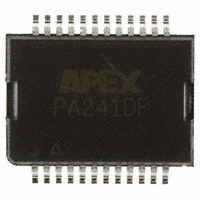
PACKAGE STYLE DF
TYPICAL APPLICATION
• PIEZO ELECTRIC POSITIONING
• ELECTROSTATIC TRANSDUCER & DEFLECTION
• DEFORMABLE MIRROR FOCUSING
• BIOCHEMISTRY STIMULATORS
• COMPUTER TO VACUUM TUBE INTERFACE
Ref: APPLICATION NOTE 20: "Bridge Mode Operation of Power Amplifiers"
R
V IN
+175
10pF
10pF
The PA241 is a high voltage monolithic MOSFET operational
amplifier which achieves performance features previously
found only in hybrid designs while increasing reliability. Inputs
are protected from excessive common mode and differential
mode voltages. The safe operating area (SOA) has no second
breakdown limitation and can be observed with all type loads
by choosing an appropriate current limiting resistor. External
compensation provides the user flexibility in choosing optimum
gain and bandwidth for the application.
The PA241CE is packaged in a hermetically sealed 8-pin
TO-3 package. The metal case of the PA241CE is isolated in
excess of full supply voltage.
The PA241DF is packaged in a 24 pin PSOP (JEDEC MO166) package. The metal heat slug of the PA241DF is isolated
in excess of full supply voltage.
The PA241DW is packaged in Apex Precision Power’s hermetic ceramic SIP package. The alumina ceramic isolates the
die in excess of full supply voltage.
+VS
20R
20R
20R
+175
DESCRIPTION
EQUIVALENT SCHEMATIC
10-PIN SIP
PACKAGE STYLE DW
A1
PA241
R CL
47
A2
PA241
R CL
Cn
LOW COST 660V p-p
PIEZO DRIVE
–175
Rn
PIEZO
TRANSDUCER 47
–175
Two PA241 amplifiers operated as a bridge driver for a piezo
transducer provides a low cost 660 volt total drive capability.
The RN CN network serves to raise the apparent gain of A2 at
high frequencies. If RN is set equal to R the amplifiers can be
compensated identically and will have matching bandwidths.
EXTERNAL CONNECTIONS
PA241CE
PA241DW
RCL
1
CC
C C1 3
OUT 4
5
–IN
2 C C2
1 ILIM
8
7
–VS
3
4
5
6
NC NC -VS +VS
7
8
9
10
ILIM CC2 CC1 OUT
CC
-IN +IN
TOP VIEW
6
+IN
2
RCL
For CC values, see graph on page 4.
Note: CC must be rated for full supply
voltage.
+VS
PA241DF
NC
NC
ILIM
+IN
-IN
PA241U
www.cirrus.com
NC
NC
NC
OUT
-IN
NC
+IN
NC
-VS
NC
NC
NC
OUT
24
+
C C2
1
-
C C1
COMP
NC
COMP
NC
NC
NC
ILIM
NC
NC
-VS
+VS
CC
RCL
NOTE: PA241CE Recommended mounting torque is 4-7
in•lbs (.45 -.79 N•m)
CAUTION: The use of compressible, thermally conductive
insulators may void warranty.
Copyright © Cirrus Logic, Inc. 2009
(All Rights Reserved)
DEC 20091
APEX − PA241UREVI
�PA241
Product Innovation From
ABSOLUTE MAXIMUM RATINGS
SUPPLY VOLTAGE, +VS to –VS
OUTPUT CURRENT, continuous within SOA
OUTPUT CURRENT, peak
POWER DISSIPATION, continuous @ TC = 25°C
INPUT VOLTAGE, differential
INPUT VOLTAGE, common mode
TEMPERATURE, pin solder – 10 sec
TEMPERATURE, junction2
TEMPERATURE, storage
TEMPERATURE RANGE, powered (case)
SPECIFICATIONS
PARAMETER
TEST CONDITIONS1
INPUT
OFFSET VOLTAGE, initial
OFFSET VOLTAGE, vs. temperature3
OFFSET VOLTAGE, vs. temperature3
OFFSET VOLTAGE, vs supply
OFFSET VOLTAGE, vs time
BIAS CURRENT, initial6
BIAS CURRENT, vs supply
OFFSET CURRENT, initial6
INPUT IMPEDANCE, DC
INPUT CAPACITANCE
COMMON MODE, voltage range
COMMON MODE, voltage range
COMMON MODE REJECTION, DC
NOISE, broad band
NOISE, low frequency
GAIN
OPEN LOOP at 15Hz
BANDWIDTH, gain bandwidth product
POWER BANDWIDTH
OUTPUT
VOLTAGE SWING
CURRENT, peak4
CURRENT, continuous
SETTLING TIME to .1%
SLEW RATE
RESISTANCE5, 1mA
RESISTANCE5, 40 mA
RL = 5K
10V step, A V = –10
CC = 3.3pF
RCL = 0
RCL = 0
POWER SUPPLY
VOLTAGE
CURRENT, quiescent
THERMAL
PA241CE RESISTANCE, AC junction to case
PA241DF RESISTANCE, AC junction to case
PA241CE RESISTANCE, DC junction to case
PA241DF RESISTANCE, DC junction to case
PA241CE RESISTANCE, junction to air
PA241DF RESISTANCE, junction to air7
TEMPERATURE RANGE, case
NOTES: *
1.
2.
3.
4.
5.
6.
7.
CAUTION
2
+VS–14
-VS+12
84
F > 60Hz
F > 60Hz
F < 60Hz
F < 60Hz
Full temperature range
Full temperature range
Meets full range spec's
25
100
270
3
70
5/50
0.2/2
2.5/50
1011
6
94
50
125
90
96
3
30
±VS–12
120
60
±VS–10
±50
±150
2.2
280V p-p
IO = 40mA
PA241DF
PA241DFA
350V
60 mA
120 mA
12W
±16 V
±VS
300°C
150°C
–65 to +150°C
–40 to +125°C
350V
60 mA
120 mA
12W
±16 V
±VS
220°C
150°C
–65 to +150°C
–40 to +125°C
PA241CE, PA241DF
MIN
TYP
MAX
MIN
25° to 85°C
-25° to 25°C
VCM = ±90V DC
10kHz BW, RS = 1K
1-10 Hz
PA241CE
PA241CEA
–25
2
30
150
5
5.4
6
9
9
30
25
PA241CEA
TYP
40
15
250
*
500
*
*
130
*
50/200
*
*
50/200
*
*
*
*
*
*
*
*
*
*
MAX
UNITS
30
*
*
mV
µV/°C
µV/°C
µV/V
µV/kh
pA
pA/V
pA
*
*
*
pF
V
V
dB
µV RMS
µV p-p
*
*
*
dB
MHz
kHz
±VS–10
±VS–8.5
*
*
*
*
*
*
±175
*
2.5
*
*
6.5
*
7
*
10.4
*
11
*
*
*
+85
*
V
mA
mA
µs
V/µs
Ω
Ω
*
2.3
V
mA
*
*
*
*
°C/W
°C/W
°C/W
°C/W
°C/W
°C/W
°C
*
"A" specification is the same as the non "A" specification.
Unless otherwise noted TC = 25°C, CC = 6.8pF. DC input specifications are ± value given. Power supply voltage is typical
rating.
Long term operation at the maximum junction temperature will result in reduced product life. Derate internal power dissipation
to achieve high MTTF. For guidance, refer to heatsink data sheet.
Sample tested by wafer to 95%.
Guaranteed but not tested.
The selected value of RCL must be added to the values given for total output resistance.
Specifications separated by / indicate values for the PA241CE and PA241DF respectively.
Rating applies with solder connection of heatslug to a minimum 1 square inch foil area of the printed circuit board.
The PA241 is constructed from MOSFET transistors. ESD handling procedures must be observed.
PA241U
�PA241
Product Innovation From
ABSOLUTE MAXIMUM RATINGS
SUPPLY VOLTAGE, +VS to –VS
OUTPUT CURRENT, continuous within SOA
OUTPUT CURRENT, peak
POWER DISSIPATION, continuous @ TC = 25°C
INPUT VOLTAGE, differential
INPUT VOLTAGE, common mode
TEMPERATURE, pin solder – 10 sec
TEMPERATURE, junction2
TEMPERATURE, storage
TEMPERATURE RANGE, powered (case)
SPECIFICATIONS
PARAMETER
TEST CONDITIONS1
INPUT
OFFSET VOLTAGE, initial
OFFSET VOLTAGE, vs. temperature3
OFFSET VOLTAGE, vs. temperature3
OFFSET VOLTAGE, vs supply
OFFSET VOLTAGE, vs time
BIAS CURRENT, initial
BIAS CURRENT, vs supply
OFFSET CURRENT, initial
INPUT IMPEDANCE, DC
INPUT CAPACITANCE
COMMON MODE, voltage range
COMMON MODE, voltage range
COMMON MODE REJECTION, DC
NOISE, broad band
NOISE, low frequency
GAIN
OPEN LOOP at 15Hz
BANDWIDTH, gain bandwidth product
POWER BANDWIDTH
OUTPUT
VOLTAGE SWING
CURRENT, peak4
CURRENT, continuous
SETTLING TIME to .1%
SLEW RATE
RESISTANCE5, 1mA
RESISTANCE5, 40 mA
25° to 85°C
-25° to 25°C
VCM = ±90V DC
10kHz BW, RS = 1K
1-10 Hz
RL = 5K
NOTES: *
1.
2.
3.
4.
5.
CAUTION
PA241U
+VS–14
-VS+12
84
IO = 40mA
10V step, A V = –10
CC = 3.3pF
RCL = 0
RCL = 0
F > 60Hz
F < 60Hz
Full temperature range
Meets full range spec's
PA241DW
TYP
25
100
270
3
70
100
15
100
1011
6
94
50
125
90
96
3
30
±VS–12
120
60
±VS–10
±50
±150
2.2
280V p-p
POWER SUPPLY
VOLTAGE
CURRENT, quiescent
THERMAL
PA241DW RESISTANCE, AC junction to case
PA241DW RESISTANCE, DC junction to case
PA241DW RESISTANCE, junction to air
TEMPERATURE RANGE, case
MIN
–25
2
30
150
5
7
12
55
PA241DW
PA241DWA
350V
60 mA
120 mA
9W
±16 V
±VS
220°C
150°C
–65 to +150°C
–40 to +125°C
MAX
MIN
PA241DWA
TYP
40
15
250
*
500
*
*
130
*
2000
*
50
*
400
*
*
*
*
*
*
*
*
*
*
MAX
UNITS
30
*
*
mV
µV/°C
µV/°C
µV/V
µV/kh
pA
pA/V
pA
*
*
*
pF
V
V
dB
µV RMS
µV p-p
*
*
*
dB
MHz
kHz
±VS–10
±VS–8.5
*
*
*
*
*
*
±175
*
2.5
*
*
10
*
14
*
*
+85
*
V
mA
mA
µs
V/µs
Ω
Ω
*
2.3
V
mA
*
*
°C/W
°C/W
°C/W
°C
*
"A" specification is the same as the non "A" specification.
Unless otherwise noted TC = 25°C, CC = 6.8pF. DC input specifications are ± value given. Power supply voltage is typical
rating.
Long term operation at the maximum junction temperature will result in reduced product life. Derate internal power dissipation
to achieve high MTTF. For guidance, refer to heatsink data sheet.
Sample tested by wafer to 95%.
Guaranteed but not tested.
The selected value of RCL must be added to the values given for total output resistance.
The PA241 is constructed from MOSFET transistors. ESD handling procedures must be observed.
3
�POWER DERATING
0.85
VBE-
0.80
0.75
VBE+
0.70
0.65
T = TA
0.60
3
0
COMPENSATION, pF
6
0.90
PA241DW
T = TC
25
50
75
100
TEMPERATURE, T (°C)
0.50
-55 -35 -15 5 25 45 65 85 105 125
TEMPERATURE, (°C)
125
SMALL SIGNAL RESPONSE
15pF
-110
60
15pF
68pF
-120
.75pF
-130
-140
68pF
6.8pF
-150
-160
0
-170
-20
10
100
1K 10K 100K 1M
FREQUENCY, F (Hz)
-180
10K
10M
100K
1M
FREQUENCY, F (Hz)
10M
SLEW RATE
HARMONIC DISTORTION
10
180V P-P
0.01
AV = 20
CC = 15pF
RL = 2K
COMMON MODE REJECTION, CMR (dB)
0.001
100
4
120
1K
10K
FREQUENCY, F (Hz)
100
80
60
40
20
0
10
10K
100
1K
FREQUENCY, F (Hz)
100K
15
5
0 10 20 30 40 50 60 70
COMPENSATION CAPACITANCE, CC (pF)
100K
COMMON MODE REJECTION
25
100
POWER SUPPLY REJECTION
TC = 55°C
1
TC = 25°C
NEGATIVE
80
70
POSITIVE
60
6.8pF
15pF
33pF
100
68pF
10
10K
100K
FREQUENCY, F (Hz)
1M
QUIESCENT CURRENT
120
115
110
°C)
I Q (85
105
°C)
I Q (25
100
)
IQ (-25°C
95
90
85
80
100 150
200 250 300 350
TOTAL SUPPLY VOLTAGE, (V)
OUTPUT VOLTAGE SWING
VDROP- @85°C
VDROP+ @85°C
8
6
VDROP+ @25°C
VDROP- @25°C
4
2
50
40
10
100
POWER RESPONSE
10
90
10
GAIN
.75pF
12
VDROP FROM VS, (V)
60V P-P
0.1
SLEW RATE, (V/µs)
30V P-P
POWER SUPPLY REJECTION, PSR (dB)
DISTORTION, (%)
35
1
TC = 85°C
1000
-100
6.8pF
20
10
0.1
1
PHASE RESPONSE
-90
.75pF
80
40
TC = 125°C
0.55
T = TA
0
GAIN AND COMPENSATION
100
OUTPUT VOLTAGE, (VOUT)(p-p)
9
PA241CE
PA241DF
T = TC
VBE (V)
12
ILIMIT VS. TEMPERATURE
0.95
NORMALIZED QUIESCENT CURRENT (%)
15
100
OPEN LOOP GAIN, A (dB)
Product Innovation From
PHASE, Ф (°)
INTERNAL POWER DISSIPATION, P(W)
PA241
100
1K
10K
FREQUENCY, F (Hz)
100K
0
0
20
40 60
80 100 120
OUTPUT CURRENT, IO (mA)
PA241U
�PA241
Product Innovation From
GENERAL
Please read Application Note 1 "General Operating Considerations" which covers stability, power supplies, heat sinking,
mounting, current limit, SOA interpretation, and specification
interpretation. Visit www.Cirrus.com for design tools that help
automate tasks such as calculations for stability, internal power
dissipation, current limit, heat sink selection, Apex Precision
Power's complete Application Notes library, Technical Seminar
Workbook and Evaluation Kits.
PHASE COMPENSATION
Open loop gain and phase shift both increase with increasing temperature. The PHASE COMPENSATION typical graph
shows closed loop gain and phase compensation capacitor
value relationships for four case temperatures. The curves are
based on achieving a phase margin of 50°. Calculate the highest case temperature for the application (maximum ambient
temperature and highest internal power dissipation) before
choosing the compensation. Keep in mind that when working
with small values of compensation, parasitics may play a large
role in performance of the finished circuit. The compensation
capacitor must be rated for at least the total voltage applied
to the amplifier and should be a temperature stable type such
as NPO or COG.
OTHER STABILITY CONCERNS
There are two important concepts about closed loop gain
when choosing compensation. They stem from the fact that
while "gain" is the most commonly used term, β (the feedback
factor) is really what counts when designing for stability.
1. Gain must be calculated as a non-inverting circuit (equal
input and feedback resistors can provide a signal gain of
-1, but for calculating offset errors, noise, and stability, this
is a gain of 2).
2. Including a feedback capacitor changes the feedback factor
or gain of the circuit. Consider Rin=4.7k, Rf=47k for a gain
of 11. Compensation of 4.7 to 6.8pF would be reasonable.
Adding 33pF parallel to the 47k rolls off the circuit at 103kHz,
and at 2MHz has reduced gain from 11 to roughly 1.5 and
the circuit is likely to oscillate.
As a general rule the DC summing junction impedance
(parallel combination of the feedback resistor and all input
resistors) should be limited to 5k ohms or less. The amplifier
input capacitance of about 6pF, plus capacitance of connecting
traces or wires and (if used) a socket will cause undesirable
circuit performance and even oscillation if these resistances
are too high. In circuits requiring high resistances, measure or
estimate the total sum point capacitance, multiply by Rin/Rf, and
parallel Rf with this value. Capacitors included for this purpose
are usually in the single digit pF range. This technique results
in equal feedback factor calculations for AC and DC cases. It
does not produce a roll off, but merely keeps β constant over
a wide frequency range. Paragraph 6 of Application Note 19
details suitable stability tests for the finished circuit.
PA241U
CURRENT LIMIT
For proper operation, the current limit resistor, Rcl, must be
connected as shown in the external connection diagram. The
minimum value is 3.9 ohms, however for optimum reliability,
the resistor should be set as high as possible. The maximum
practical value is 110 ohms. Current limit values can be predicted as follows:
Ilimit = Vbe
Rcl
Where Vbe is shown in the CURRENT LIMIT typical
graph.
Note that +Vbe should be used to predict current through
the +Vs pin, -Vbe for current through the -Vs pin, and that they
vary with case temperature. Value of the current limit resistor
at a case temperature of 25° can be estimated as follows:
Rcl = 0.7
Ilimit
When the amplifier is current limiting, there may be spurious
oscillation present during the current limited portion of the negative half cycle. The frequency of the oscillation is not predictable
and depends on the compensation, gain of the amplifier, value
of the current limit resistor, and the load. The oscillation will
cease as the amplifier comes out of current limit.
SAFE OPERATING AREA
The MOSFET output stage of the PA241 is not limited by
second breakdown considerations as in bipolar output stages.
However there are still three distinct limitations:
1. Voltage withstand capability of the transistors.
2. Current handling capability of the die metalization.
3. Temperature of the output MOSFETS.
These limitations can be seen in the SOA (see Safe Operating Area graphs). Note that each pulse capability line shows
a constant power level (unlike second breakdown limitations
where power varies with voltage stress). These lines are shown
for a case temperature of 25°C and correspond to thermal
resistances of 5.2°C/W for the PA241CE and DF and 10.4°C/W
for the PA241DW respectively. Pulse stress levels for other
case temperatures can be calculated in the same manner as
DC power levels at different temperatures. The output stage
is protected against transient flyback by the parasitic diodes of
the output stage MOSFET structure. However, for protection
against sustained high energy flyback external fast-recovery
diodes must be used.
HEATSINKING
The PA241DF package has a large exposed integrated
copper heatslug to which the monolithic amplifier is directly
attached. The solder connection of the heatslug to a minimum
of 1 square inch foil area on the printed circuit board will result
in thermal performance of 25°C/W junction to air rating of the
PA241DF. Solder connection to an area of 1 to 2 square inches
is recommended. This may be adequate heatsinking but the
large number of variables involved suggest temperature measurements be made on the top of the package. Do not allow
the temperature to exceed 85°C.
5
�PA241
200
Product Innovation From
PA241CE and DF SOA
+Vs
OUTPUT CURRENT FROM +VS OR –VS, (mA)
0m
100
S
50
40
DC
DC
,T
30
=
C
20
,T
=
12
5°
C
Z2
OVERVOLTAGE PROTECTION
PULSE CURVES @ 10% DUTY CYCLE MAX
20 30
50
100
200 300
500
SUPPLY TO OUTPUT DIFFERENTIAL, VS -VO (V)
PA241DW SOA
120
20
0m
S
50
40
DC
DC
30
,T
DC
C
,T
C
=
=
85
°C
12
5°
C
5
4
3
2
10
-Vs
FIGURE 1
100
10
OUT
Q2
-Vs
5
4
20
+IN
°C
C
200
Q1
85
DC
10
2
10
OUTPUT CURRENT FROM +VS OR –VS, (mA)
+Vs
-IN
3
Z1
20
120
PULSE CURVES @ 10% DUTY CYCLE MAX
20 30
50
100
200 300
500
SUPPLY TO OUTPUT DIFFERENTIAL, VS -VO (V)
Although the PA241 can withstand differential input voltages
up to 16V, in some applications additional external protection
may be needed. Differential inputs exceeding 16V will be clipped
by the protection circuitry. However, if more than a few milliamps
of current is available from the overload source, the protection
circuitry could be destroyed. For differential sources above
16V, adding series resistance limiting input current to 1mA will
prevent damage.Alternatively, 1N4148 signal diodes connected
anti-parallel across the input pins is usually sufficient. In more
demanding applications where bias current is important, diode
connected JFETs such as 2N4416 will be required. See Q1
and Q2 in Figure 1. In either case the differential input voltage
will be clamped to 0.7V. This is sufficient overdrive to produce
the maximum power bandwidth.
In the case of inverting circuits where the +IN pin is grounded,
the diodes mentioned above will also afford protection from
excessive common mode voltage. In the case of non-inverting circuits, clamp diodes from each input to each supply will
provide protection. Note that these diodes will have substantial
reverse bias voltage under normal operation and diode leakage will produce errors.
Some applications will also need over-voltage protection
devices connected to the power supply rails. Unidirectional
zener diode transient suppressors are recommended. The
zeners clamp transients to voltages within the power supply
rating and also clamp power supply reversals to ground.
Whether the zeners are used or not the system power supply
should be evaluated for transient performance including poweron overshoot and power-off polarity reversals as well as line
regulation. See Z1 and Z2 in Figure 1.
APPLICATION REFERENCES:
For additional technical information please refer to the following Application Notes:
AN1: General Operating Considerations
AN3: Bridge Circuit Drives
AN25: Driving Capacitive Loads
AN38: Loop Stability with Reactive Loads
6
PA241U
�Product Innovation From
PA241
CONTACTING CIRRUS LOGIC SUPPORT
For all Apex Precision Power product questions and inquiries, call toll free 800-546-2739 in North America.
For inquiries via email, please contact apex.support@cirrus.com.
International customers can also request support by contacting their local Cirrus Logic Sales Representative.
To find the one nearest to you, go to www.cirrus.com
IMPORTANT NOTICE
Cirrus Logic, Inc. and its subsidiaries ("Cirrus") believe that the information contained in this document is accurate and reliable. However, the information is subject
to change without notice and is provided "AS IS" without warranty of any kind (express or implied). Customers are advised to obtain the latest version of relevant
information to verify, before placing orders, that information being relied on is current and complete. All products are sold subject to the terms and conditions of sale
supplied at the time of order acknowledgment, including those pertaining to warranty, indemnification, and limitation of liability. No responsibility is assumed by Cirrus
for the use of this information, including use of this information as the basis for manufacture or sale of any items, or for infringement of patents or other rights of third
parties. This document is the property of Cirrus and by furnishing this information, Cirrus grants no license, express or implied under any patents, mask work rights,
copyrights, trademarks, trade secrets or other intellectual property rights. Cirrus owns the copyrights associated with the information contained herein and gives consent for copies to be made of the information only for use within your organization with respect to Cirrus integrated circuits or other products of Cirrus. This consent
does not extend to other copying such as copying for general distribution, advertising or promotional purposes, or for creating any work for resale.
CERTAIN APPLICATIONS USING SEMICONDUCTOR PRODUCTS MAY INVOLVE POTENTIAL RISKS OF DEATH, PERSONAL INJURY, OR SEVERE PROPERTY OR ENVIRONMENTAL DAMAGE (“CRITICAL APPLICATIONS”). CIRRUS PRODUCTS ARE NOT DESIGNED, AUTHORIZED OR WARRANTED TO BE
SUITABLE FOR USE IN PRODUCTS SURGICALLY IMPLANTED INTO THE BODY, AUTOMOTIVE SAFETY OR SECURITY DEVICES, LIFE SUPPORT PRODUCTS OR OTHER CRITICAL APPLICATIONS. INCLUSION OF CIRRUS PRODUCTS IN SUCH APPLICATIONS IS UNDERSTOOD TO BE FULLY AT THE CUSTOMER’S RISK AND CIRRUS DISCLAIMS AND MAKES NO WARRANTY, EXPRESS, STATUTORY OR IMPLIED, INCLUDING THE IMPLIED WARRANTIES OF
MERCHANTABILITY AND FITNESS FOR PARTICULAR PURPOSE, WITH REGARD TO ANY CIRRUS PRODUCT THAT IS USED IN SUCH A MANNER. IF THE
CUSTOMER OR CUSTOMER’S CUSTOMER USES OR PERMITS THE USE OF CIRRUS PRODUCTS IN CRITICAL APPLICATIONS, CUSTOMER AGREES,
BY SUCH USE, TO FULLY INDEMNIFY CIRRUS, ITS OFFICERS, DIRECTORS, EMPLOYEES, DISTRIBUTORS AND OTHER AGENTS FROM ANY AND ALL
LIABILITY, INCLUDING ATTORNEYS’ FEES AND COSTS, THAT MAY RESULT FROM OR ARISE IN CONNECTION WITH THESE USES.
Cirrus Logic, Cirrus, and the Cirrus Logic logo designs, Apex Precision Power, Apex and the Apex Precision Power logo designs are trademarks of Cirrus Logic, Inc.
All other brand and product names in this document may be trademarks or service marks of their respective owners.
PA241U
7
�