Data Sheet
ACPL-077L
Low-Power 3.3V/5V High-Speed CMOS
Optocoupler Design for System-Level
Reliability
Description
Features
The Broadcom® ACPL-077L optocoupler utilizes the latest
CMOS IC technology to achieve outstanding speed and low
power performance of minimum 25-MBd data rate and 6-ns
maximum pulse width distortion with enhanced reliability
relative to system-level IEC 61000-4-X testing (ESD/Burst/
Surge).
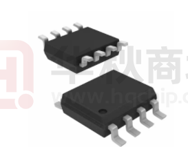
Available in SO-8 package, the basic building blocks of
ACPL-077L are a CMOS LED driver IC, a high-speed LED,
and a CMOS detector IC. A CMOS logic input signal
controls the LED driver IC, which supplies current to the
LED. The detector IC incorporates an integrated
photodiode, a high-speed transimpedance amplifier, and a
voltage comparator with an output driver.
CAUTION! It is advised that normal static precautions be
taken in handling and assembly of this
component to prevent damage and/or
degradation, which may be induced by ESD.
The components featured in this data sheet are
not to be used in military or aerospace
applications or environments.
Applications
Broadcom
Enhance reliability relative to system-level
IEC 61000-4-Xtesting (ESD/Burst/Surge)
3.3V and 5V CMOS compatibility
CMOS buffer input
Allow level shifting functionality
High speed: DC to 25 MBd
35-kV/µs minimum common mode rejection (CMR) at
VCM = 1000V
Guaranteed AC and DC performance over wide
temperature:–40 to +105°C
Safety and regulatory approvals:
– UL recognized:
3750 Vrms for 1 min. per UL1577
– CSA component acceptance notice #5
– IEC/EN/DIN EN 60747-5-5:
VIORM = 567 Vpeak for Option 060E
Lead-free option available
Digital fieldbus isolation: CC-Link, DeviceNet, Profibus,
SDS
Multiplexed data transmission
General instrument and data acquisition
Computer peripheral interface
Microprocessor system interface
AV02-3547EN
January 12, 2018
�ACPL-077L Data Sheet
Low-Power 3.3V/5V High-Speed CMOS Optocoupler Design for System-Level Reliability
Functional Diagram
Truth Table
8 VDD2**
**VDD1 1
VI 2
7 NC*
VI
LED1
VO
HIGH
LOW
OFF
ON
HIGH
LOW
IO
NC* 3
6 VO
LED1
GND1 4
*
SHIELD
5 GND2
Pin 3 is multiplexed as a test pin that can connect to VDD or
left unconnected. Pin 7 is not connected internally.
** A 0.01 μF to 0.1 μF bypass capacitor must be connected as
close as possible between pins VDD1 and GND1, and VDD2
and GND2.
Ordering Information
ACPL-077L is UL Recognized with 3750 Vrms for 1 minute per UL1577.
Option
Part Number
ACPL-077L
RoHS Compliant
Package
Surface
Mount
-000E
SO-8
X
-060E
Tape
and Reel
IEC/EN/DIN EN
60747-5-5
Quantity
100 per tube
X
-500E
X
X
-560E
X
X
X
100 per tube
X
1500 per reel
1500 per reel
To order, choose a part number from the part number column and combine with the desired option from the option column
to form an order entry.
Example 1:
ACPL-077L-500E to order product of Mini-flat Surface Mount 8-pin package in Tape and Reel packaging with RoHS
compliant.
Option data sheets are available. Contact your Broadcom sales representative or authorized distributor for information.
Regulatory Information
The ACPL-077L will be approved by the following organizations:
UL — Approval under UL 1577, component recognition program up to VISO = 3750 VRMS.
CSA — Approval under CSA component acceptance notice #5.
IEC/EN/DIN EN 60747-5-5 — (Option 060E only)
Broadcom
AV02-3547EN
2
�ACPL-077L Data Sheet
Low-Power 3.3V/5V High-Speed CMOS Optocoupler Design for System-Level Reliability
Package Outline Drawings
ACPL-077L SO-8 Package
LAND PATTERN RECOMMENDATION
1.91
(0.075)
0.64
(0.025)
3.937 ± 0.127
(0.155 ± 0.005)
8
7
6
5
NNNN Z
YYWW
EEE
DEVICE PART
NUMBER
LEAD-FREE
•
PIN 1
1
2
3
TEST RATING CODE
LOT ID
4
0.406 ± 0.076
(0.016 ± 0.003)
7.49
(0.295)
DATE CODE
5.994 ± 0.203
(0.236 ± 0.008)
1.27
(0.5)
1.270 BSC
(0.050)
* 5.080 ± 0.127
(0.200 ± 0.005)
3.175 ± 0.127
(0.125 ± 0.005)
7°
1.524
(0.060)
* Total package length (inclusive of mold flash)
5.207 ± 0.254 (0.205 ± 0.010)
Dimensions in Millimeters (Inches).
Note: Floating lead protrusion is 0.15 mm (6 mils) max.
Lead coplanarity = 0.10 mm (0.004 inches) max.
Option number 500 not marked.
0.432
45° X (0.017)
0 ~ 7°
0.228 ± 0.025
(0.009 ± 0.001)
0.203 ± 0.102
(0.008 ± 0.004)
0.305 MIN.
(0.012)
Solder Reflow Profile
Recommended reflow condition as per JEDEC Standard, J-STD-020 (latest revision). Non-Halide Flux should be used.
Broadcom
AV02-3547EN
3
�ACPL-077L Data Sheet
Low-Power 3.3V/5V High-Speed CMOS Optocoupler Design for System-Level Reliability
Insulation and Safety Related Specifications
Parameter
Symbol
ACPL-077L
Unit
Minimum External Air Gap
(Clearance)
L(I01)
4.9
mm
Measured from input terminals to output terminals,
shortest distance through air.
Minimum External Tracking
(Creepage)
L(I02)
4.8
mm
Measured from input terminals to output terminals,
shortest distance path along body.
0.08
mm
Through insulation distance conductor to conductor,
usually the straight line distance thickness between
the emitter and detector.
175
V
Minimum Internal Plastic Gap
(Internal Clearance)
Tracking Resistance
(Comparative Tracking Index)
CTI
Isolation Group
IIIa
Conditions
DIN IEC 112/VDE 0303 Part 1.
Material Group (DIN VDE 0110, 1/89, Table 1).
IEC/EN/DIN EN 60747-5-5 Insulation Characteristics (Option 060E)
Characteristic
Description
Symbol
Installation Classification per DIN VDE 0110/39, Table 1
For Rated Mains Voltage ≤ 150Vrms
ACPL-077L
Unit
I – IV
I – III
I – II
For Rated Mains Voltage ≤ 300Vrms
For Rated Mains Voltage ≤ 600Vrms
Climatic Classification
55/105/21
Pollution Degree (DIN VDE 0110/39)
2
VIORM
567
Vpeak
Input to Output Test Voltage, Method ba
VIORM x 1.875 = VPR, 100% Production Test with tm = 1s,
Partial Discharge < 5 pC
VPR
1063
Vpeak
Input to Output Test Voltage, Method aa
VIORM x 1.6 = VPR, Type and Sample Test, tm = 10s,
Partial Discharge < 5 pC
VPR
907
Vpeak
VIOTM
6000
Vpeak
TS
IS, INPUT
PS, OUTPUT
150
150
600
°C
mA
mW
RS
≥109
Ω
Maximum Working Insulation Voltage
Highest Allowable Overvoltage (Transient Overvoltage tini = 60s)
Safety-Limiting Values – Maximum Values Allowed in the Event of a Failure
Case Temperature
b
Input Current
Output Power
Insulation Resistance at TS, VIO = 500V
a. Refer to the optocoupler section of the Isolation and Control Component Designer’s Catalog, under Product Safety Regulations section (IEC/
EN/DIN EN 60747-5-5) for a detailed description of Method a and Method b partial discharge test profiles.
b. Refer to figure 10 for dependence of PS and IS on ambient temperature.
NOTE:
Broadcom
These optocouplers are suitable for safe electrical isolation only within the safety limit data. Maintenance of the
safety data is ensured by means of protective circuits.
AV02-3547EN
4
�ACPL-077L Data Sheet
Low-Power 3.3V/5V High-Speed CMOS Optocoupler Design for System-Level Reliability
Absolute Maximum Ratings
Parameter
Symbol
Min.
Max.
Unit
Storage Temperature
TS
–55
125
°C
Operating Temperature
TA
–40
105
°C
VDD1, VDD2
0
6.5
V
Input Voltage
VI
–0.5
VDD1 + 0.5
V
Output Voltage
VO
–0.5
VDD2 + 0.5
V
Average Output Current
IO
—
10
mA
Supply Voltages
Lead Solder Temperature
TLS
260° C for 10 sec., 1.6 mm below seating plane
Solder Reflow Temperature Profile
See Solder Reflow Profile section.
Recommended Operating Conditions
Parameter
Symbol
Min.
Max.
Unit
Operating Temperature
TA
–40
105
°C
Supply Voltages (3.3V)
VDD1, VDD2
3.0
3.6
V
Supply Voltages (5V)
VDD1, VDD2
4.5
5.5
V
Logic High Input Voltage
VIH
0.7 x VDD1
VDD1
V
Logic Low Input Voltage
VIL
0
0.3 x VDD1
V
tir, tif
—
1.0
ms
Input Signal Rise and Fall Times
Electrical Specifications
Over recommended temperature (TA = –40°C to 105°C) and supply voltage (4.5V ≤ VDD1 ≤ 5.5V, 4.5V ≤ VDD2 ≤ 5.5V),
(3V ≤ VDD1 ≤ 3.6V, 3V ≤ VDD2 ≤ 3.6V), (4.5V ≤ VDD1 ≤ 5.5V, 3V ≤ VDD2 ≤ 3.6V) and (3V ≤ VDD1 ≤ 3.6V, 4.5V ≤ VDD2 ≤ 5.5V).
All typical specifications are at VDD1 = VDD2 = +3.3V, TA = 25°C.
Parameter
Symbol
Min.
Typ.
Max.
Unit
Logic Low Input Supply Currenta
IDD1L
—
5.5
8
mA
VI = 0V; Figure 1
Logic High Input Supply Currenta
IDD1H
—
0.6
2
mA
VI = VDD1; Figure 2
Logic Low Output Supply Current
IDD2L
—
1.5
2.5
mA
VI = 0V; Figure 3
Logic High Output Supply Current
IDD2H
—
1.5
2.5
mA
VI = VDD1; Figure 4
II
–10
—
10
μA
VOH
2.9
3.3
—
V
1.9
2.9
4.0
4.7
—
V
IO = –4 mA, VI = VIH, VDD2 = 5.0V
—
0
0.1
V
IO = 20 μA, VI = VIL
—
0.35
1.0
V
IO = 4 mA, VI = VIL
Input Current
Logic High Output Voltage
Logic Low Output Voltage
VOL
Test Conditions
IO = –20 μA, VI = VIH, VDD2 = 3.3V
IO = –4 mA, VI = VIH, VDD2 = 3.3V
a. The LED is ON when VI is low and OFF when VI is high.
Broadcom
AV02-3547EN
5
�ACPL-077L Data Sheet
Low-Power 3.3V/5V High-Speed CMOS Optocoupler Design for System-Level Reliability
Switching Specifications
Over recommended temperature (TA = –40°C to 105°C) and supply voltage (4.5V ≤ VDD1 ≤ 5.5V, 4.5V ≤ VDD2 ≤ 5.5V),
(3V ≤ VDD1 ≤ 3.6V, 3V ≤ VDD2 ≤ 3.6V), (4.5V ≤ VDD1 ≤ 5.5V, 3V ≤ VDD2 ≤ 3.6V) and (3V ≤ VDD1 ≤ 3.6V, 4.5V ≤ VDD2 ≤ 5.5V).
All typical specifications are at VDD1 = VDD2 = +3.3V, TA = 25°C.
Parameter
Symbol
Min.
Typ.
Max.
Unit
Test Conditions
Propagation Delay Time to Logic Low
Outputa
tPHL
—
24
40
ns
CL = 15 pF, CMOS Signal Levels; Figure 5
and Figure 6.
Propagation Delay Time to Logic High
Outputa
tPLH
—
23
40
ns
CL = 15 pF, CMOS Signal Levels; Figure 5
and Figure 6.
Pulse Width
tPW
40
—
—
ns
CL = 15 pF, CMOS Signal Levels.
—
—
25
MBd
CL = 15 pF, CMOS Signal Levels.
|PWD|
—
1
6
ns
CL = 15 pF, CMOS Signal Levels; Figure 7
and Figure 8.
tPSK
—
—
15
ns
CL = 15 pF, CMOS Signal Levels.
Output Rise Time (10% to 90%)
tR
—
4
—
ns
CL = 15 pF, CMOS Signal Levels, Figure 9.
Output Fall Time (90% to 10%)
tF
—
3
—
ns
Common Mode Transient Immunity at
Logic High Outputd
|CMH|
35
50
—
kV/μs
VCM = 1000V, TA = 25°C,
VI = VDD1, VO > 0.8 × VDD2.
Common Mode Transient Immunity at
Logic Low Outputd
|CML|
35
50
—
kV/μs
VCM = 1000V, TA = 25°C,
VI = 0V, VO < 0.8V.
Maximum Data Rate
Pulse Width
Distortionb
|tPHL – tPLH|
Propagation Delay Skewc
a. tPHL propagation delay is measured from the 50% level on the falling edge of the VI signal to the 50% level of the falling edge of the VO signal.
tPLH propagation delay is measured from the 50% level on the rising edge of the VI signal to the 50% level of the rising edge of the VO signal.
b. PWD is defined as |tPHL – tPLH|. %PWD (percent pulse width distortion) is equal to the PWD divided by pulse width.
c. tPSK is equal to the magnitude of the worst-case difference in tPHL and/or tPLH that will be seen between units at any given temperature within
the recommended operating conditions.
d. CMH is the maximum common mode voltage slew rate that can be sustained while maintaining VO > 0.8 VDD2. CML is the maximum common
mode voltage slew rate that can be sustained while maintaining VO < 0.8V. The common mode voltage slew rates apply to both rising and
falling common mode voltage edges.
Package Characteristics
All typical specifications are at TA = 25°C.
Parameter
Symbol
Min.
Typ.
Max.
Unit
Input-Output Insulation a, b, c
VISO
3750
—
—
Vrms
Input-Output Resistancea
RI-O
—
1012
—
Ω
VI-O = 500V
Input-Output Capacitance
CI-O
—
0.6
—
pF
f = 1 MHz, TA = 25°C
CI
—
3.0
—
pF
Input Capacitanced
Test Conditions
RH ≤ 50% for 1 min, TA = 25°C
a. Device considered a two-terminal device: pins 1, 2, 3, and 4 shorted together and pins 5, 6, 7, and 8 shorted together.
b. In accordance with UL1577, each ACPL-077L is proof tested by applying an insulation test voltage ≥ 4500 VRMS for 1 second (leakage
detection current limit, II-O ≤ 5 μA).
c. The Input-Output Momentary Withstand Voltage is a dielectric voltage rating that should not be interpreted as an input-output continuous
voltage rating. For the continuous voltage rating, refer to your equipment level safety specification or Broadcom Application Note 1074,
Optocoupler Input-Output Endurance Voltage.
d. CI is the capacitance measured at pin 2 (VI).
Broadcom
AV02-3547EN
6
�ACPL-077L Data Sheet
Low-Power 3.3V/5V High-Speed CMOS Optocoupler Design for System-Level Reliability
6.5
6.3
6.1
5.9
5.7
5.5
5.3
5.1
4.9
4.7
4.5
-40
5V
3.3 V
-20
0
20
40
TA (°C)
60
80
100
1.6
1.6
1.5
1.5
1.4
1.3
1.2
1.1
1.0
5V
3.3 V
0.9
0.8
-40
-20
0
20
40
TA (°C)
60
80
-40
-20
0
20
40
TA (°C)
Broadcom
60
80
100
-20
0
20
40
TA (°C)
60
80
100
1.3
1.2
1.1
1
5V
3.3 V
0.9
-20
0
20
40
TA (°C)
60
80
100
Figure 6: Typical Propagation Delays vs. Load Capacitance at
3.3V Supply Voltage
Tphl, Tplh (ns)
Tplh
Tphl
5V
3.3 V
1.4
0.8
-40
100
Figure 5: Typical Propagation Delay vs. Temperature at 3.3V
Supply Voltage
Tphl, Tplh (ns)
0.6
0.58
0.56
0.54
0.52
0.5
0.48
0.46
0.44
0.42
0.4
-40
Figure 4: Typical Logic High Output Supply Current vs.
Temperature
IDD2H - LOGIC HIGH OUTPUT SUPPLY
CURRENT - mA
IDD2L - LOGIC LOW OUTPUT SUPPLY
CURRENT - mA
Figure 3: Typical Logic Low Output Supply Current vs.
Temperature
35
33
31
29
27
25
23
21
19
17
15
Figure 2: Typical Logic High Input Supply Current vs.
Temperature
IDD1H - LOGIC HIGH INPUT SUPPLY
CURRENT - mA
IDD1L - LOGIC LOW INPUT SUPPLY
CURRENT - mA
Figure 1: Typical Logic Low Input Supply Current vs.
Temperature
30
29
28
27
26
25
24
23
22
21
20
Tplh
Tphl
15
25
35
CL (pF)
45
55
AV02-3547EN
7
�ACPL-077L Data Sheet
Low-Power 3.3V/5V High-Speed CMOS Optocoupler Design for System-Level Reliability
2
1.8
1.6
1.4
1.2
1
0.8
0.6
0.4
0.2
0
6
5
4
3
2
1
0
-40
-20
0
20
40
TA (°C)
60
80
100
Figure 9: Typical Rise and Fall Time vs Temperature at 3.3V
Supply Voltage
6
15
25
35
CL (pF)
45
55
Figure 10: Thermal Derating Curve, Dependence of Safety
Limiting Value with Case Temperature per IEC/EN/DIN EN
60747-5-5
Output Power - Ps, Input Current - Is
1000
5
Tr, Tf (ns)
Figure 8: Typical Pulse Width Distortion vs Load Capacitance
at 3.3V Supply Voltage
PWD (ns)
PWD (ns)
Figure 7: Typical Pulse Width Distortion vs Temperature at
3.3V Supply Voltage
4
3
2
Rise Time
Fall Time
1
-40
-20
0
20
40
TA (°C)
Broadcom
60
80
100
Is (mA)
Ps (mW)
800
600
400
200
0
0
25
50
75
100
125
TA - Case Temperature - °C
150
175
AV02-3547EN
8
�ACPL-077L Data Sheet
Low-Power 3.3V/5V High-Speed CMOS Optocoupler Design for System-Level Reliability
Application Information
Bypassing and PC Board Layout
The ACPL-077L optocoupler is extremely easy to use. No external interface circuitry is required because ACPL-077L uses
high-speed CMOS IC technology, allowing CMOS logic to be connected directly to the inputs and outputs.
As shown in Figure 11, the only external components required for proper operation are two bypass capacitors. Capacitor
values should be between 0.01 μF and 0.1 μF. Each capacitor should be placed as close as possible to the input and output
power-supply pins of the optocoupler.
Figure 11: Recommended Circuit Diagram
VDD1
1
VI
C2
2
GND1
VDD2
8
C1
7 NC
* 3
6
4
5
VO
GND2
C1, C2 = 0.01 PF TO 0.1 PF
*
Pin 3 is multiplexed as a test pin that can connect to VDD or
left unconnected. Pin 7 is not connected internally.
Broadcom
AV02-3547EN
9
�Broadcom, the pulse logo, Connecting everything, Avago Technologies, Avago, and the A logo are among the trademarks
of Broadcom and/or its affiliates in the United States, certain other countries and/or the EU.
Copyright © 2017–2018 Broadcom. All Rights Reserved.
The term “Broadcom” refers to Broadcom Limited and/or its subsidiaries. For more information, please visit
www.broadcom.com.
Broadcom reserves the right to make changes without further notice to any products or data herein to improve reliability,
function, or design. Information furnished by Broadcom is believed to be accurate and reliable. However, Broadcom does
not assume any liability arising out of the application or use of this information, nor the application or use of any product or
circuit described herein, neither does it convey any license under its patent rights nor the rights of others.
�


 工商网监
湘ICP备2023018690号
工商网监
湘ICP备2023018690号
